JP5881676B2 - Electronic article for display and manufacturing method thereof - Google Patents
Electronic article for display and manufacturing method thereof Download PDFInfo
- Publication number
- JP5881676B2 JP5881676B2 JP2013502623A JP2013502623A JP5881676B2 JP 5881676 B2 JP5881676 B2 JP 5881676B2 JP 2013502623 A JP2013502623 A JP 2013502623A JP 2013502623 A JP2013502623 A JP 2013502623A JP 5881676 B2 JP5881676 B2 JP 5881676B2
- Authority
- JP
- Japan
- Prior art keywords
- dielectric constant
- conductive
- substrate
- composite material
- layer
- Prior art date
- Legal status (The legal status is an assumption and is not a legal conclusion. Google has not performed a legal analysis and makes no representation as to the accuracy of the status listed.)
- Expired - Fee Related
Links
Images


Classifications
-
- H—ELECTRICITY
- H05—ELECTRIC TECHNIQUES NOT OTHERWISE PROVIDED FOR
- H05B—ELECTRIC HEATING; ELECTRIC LIGHT SOURCES NOT OTHERWISE PROVIDED FOR; CIRCUIT ARRANGEMENTS FOR ELECTRIC LIGHT SOURCES, IN GENERAL
- H05B33/00—Electroluminescent light sources
- H05B33/12—Light sources with substantially two-dimensional radiating surfaces
- H05B33/14—Light sources with substantially two-dimensional radiating surfaces characterised by the chemical or physical composition or the arrangement of the electroluminescent material, or by the simultaneous addition of the electroluminescent material in or onto the light source
- H05B33/145—Arrangements of the electroluminescent material
-
- G—PHYSICS
- G09—EDUCATION; CRYPTOGRAPHY; DISPLAY; ADVERTISING; SEALS
- G09F—DISPLAYING; ADVERTISING; SIGNS; LABELS OR NAME-PLATES; SEALS
- G09F9/00—Indicating arrangements for variable information in which the information is built-up on a support by selection or combination of individual elements
- G09F9/30—Indicating arrangements for variable information in which the information is built-up on a support by selection or combination of individual elements in which the desired character or characters are formed by combining individual elements
-
- H—ELECTRICITY
- H01—ELECTRIC ELEMENTS
- H01B—CABLES; CONDUCTORS; INSULATORS; SELECTION OF MATERIALS FOR THEIR CONDUCTIVE, INSULATING OR DIELECTRIC PROPERTIES
- H01B3/00—Insulators or insulating bodies characterised by the insulating materials; Selection of materials for their insulating or dielectric properties
- H01B3/002—Inhomogeneous material in general
- H01B3/004—Inhomogeneous material in general with conductive additives or conductive layers
-
- H—ELECTRICITY
- H01—ELECTRIC ELEMENTS
- H01B—CABLES; CONDUCTORS; INSULATORS; SELECTION OF MATERIALS FOR THEIR CONDUCTIVE, INSULATING OR DIELECTRIC PROPERTIES
- H01B3/00—Insulators or insulating bodies characterised by the insulating materials; Selection of materials for their insulating or dielectric properties
- H01B3/02—Insulators or insulating bodies characterised by the insulating materials; Selection of materials for their insulating or dielectric properties mainly consisting of inorganic substances
- H01B3/12—Insulators or insulating bodies characterised by the insulating materials; Selection of materials for their insulating or dielectric properties mainly consisting of inorganic substances ceramics
-
- H—ELECTRICITY
- H01—ELECTRIC ELEMENTS
- H01B—CABLES; CONDUCTORS; INSULATORS; SELECTION OF MATERIALS FOR THEIR CONDUCTIVE, INSULATING OR DIELECTRIC PROPERTIES
- H01B5/00—Non-insulated conductors or conductive bodies characterised by their form
- H01B5/14—Non-insulated conductors or conductive bodies characterised by their form comprising conductive layers or films on insulating-supports
-
- H—ELECTRICITY
- H05—ELECTRIC TECHNIQUES NOT OTHERWISE PROVIDED FOR
- H05B—ELECTRIC HEATING; ELECTRIC LIGHT SOURCES NOT OTHERWISE PROVIDED FOR; CIRCUIT ARRANGEMENTS FOR ELECTRIC LIGHT SOURCES, IN GENERAL
- H05B33/00—Electroluminescent light sources
- H05B33/02—Details
- H05B33/04—Sealing arrangements, e.g. against humidity
-
- H—ELECTRICITY
- H05—ELECTRIC TECHNIQUES NOT OTHERWISE PROVIDED FOR
- H05B—ELECTRIC HEATING; ELECTRIC LIGHT SOURCES NOT OTHERWISE PROVIDED FOR; CIRCUIT ARRANGEMENTS FOR ELECTRIC LIGHT SOURCES, IN GENERAL
- H05B33/00—Electroluminescent light sources
- H05B33/12—Light sources with substantially two-dimensional radiating surfaces
- H05B33/22—Light sources with substantially two-dimensional radiating surfaces characterised by the chemical or physical composition or the arrangement of auxiliary dielectric or reflective layers
Description
本開示は、ディスプレイ装置において有用な電子物品、及びその物品の製造方法に関する。 The present disclosure relates to an electronic article useful in a display device, and a method of manufacturing the article.
電気活性材料とは、高い電場に反応して、光学的又は機械的効果を生じる材料である。例えばエレクトロルミネセント装置は、電場と結合されると、直接、又は放射されるエネルギーを吸収して、それを異なる波長で再放射する中間層を介して、放射光を放射することが可能な蛍光体層(電気活性材料)を有している。一般的に、エレクトロルミネセント装置は、パターン化することが可能な導電層を、基板、通常はガラス又は可撓性ポリマーの上に成膜することによって製造される。次いで、蛍光体などの電気活性材料を導電層の上に塗布することができる。次いで電気活性層を含む層を、その上に塗布されうる透明電極から保護するために、薄い誘電材料で被覆する。2層の電極と、それらの間に挟まれた電気活性層を有するこうした種類の装置は、容量性の装置であり、エネルギーを貯蔵することができる。容量性装置では、電気活性層にエネルギーを付与するために、一方の電極によって形成された電場が他方の電極に届くことが極めて重要である。短絡を生じさせて、装置を動作不能とする、導電経路が2層の電極間に実質上存在しないことも同様に重要である。 An electroactive material is a material that reacts to a high electric field to produce an optical or mechanical effect. For example, an electroluminescent device, when combined with an electric field, can emit radiation directly or through an intermediate layer that absorbs emitted energy and re-emits it at a different wavelength. It has a body layer (electroactive material). In general, electroluminescent devices are manufactured by depositing a patternable conductive layer on a substrate, usually glass or a flexible polymer. An electroactive material such as a phosphor can then be applied over the conductive layer. The layer containing the electroactive layer is then coated with a thin dielectric material to protect it from the transparent electrode that can be applied thereon. This type of device having two layers of electrodes and an electroactive layer sandwiched between them is a capacitive device and can store energy. In capacitive devices, it is very important that the electric field formed by one electrode reaches the other electrode in order to impart energy to the electroactive layer. It is equally important that there is virtually no conductive path between the two layers of electrodes that causes a short circuit and renders the device inoperable.
一般的に、コンデンサ又は容量性装置の2枚のプレートの間には、誘電体又は絶縁材料が置かれる。2枚のプレート間の電場を支持するためには、この誘電体は、極めて薄いものとするか、高い誘電率を有するか、又は両者の組み合わせである必要がある。一部の容量性装置では、極めて高い誘電率を有する無機材料が誘電材料として使用されている。例えば、チタン酸バリウムをエレクトロルミネセント装置の誘電体として使用することが知られている。酸化アルミニウム又は酸化チタンなどの非導電性金属酸化物を、容量性装置の誘電体として使用することもできる。このような無機誘電体は、蒸着法によって容量性装置に組み込むことができる。また、非エネルギー吸収性基質又は結合剤を使用し、高い誘電率を有する粒子をこれに添加することによって、複合材料を形成することもできる。一般的な結合剤は比較的低い誘電率を有していることから、容量性装置の電場を支持するだけの充分に高い誘電率を得るためには、結合剤に大量の充填剤粒子を添加する必要がある。 In general, a dielectric or insulating material is placed between two plates of a capacitor or capacitive device. In order to support the electric field between the two plates, the dielectric must be very thin, have a high dielectric constant, or a combination of both. In some capacitive devices, an inorganic material having a very high dielectric constant is used as the dielectric material. For example, it is known to use barium titanate as a dielectric for electroluminescent devices. Non-conductive metal oxides such as aluminum oxide or titanium oxide can also be used as a dielectric for capacitive devices. Such inorganic dielectrics can be incorporated into capacitive devices by vapor deposition. A composite material can also be formed by using a non-energy absorbing substrate or binder and adding particles with a high dielectric constant thereto. Because common binders have a relatively low dielectric constant, a large amount of filler particles can be added to the binder to obtain a sufficiently high dielectric constant to support the electric field of the capacitive device. There is a need to.
したがって、高い誘電率を有し、誘電損失が低いばかりでなく、極めて低い導電率を有する、電子装置において有用な絶縁材料が求められている。容量性装置である、コンデンサ、アクチュエーター、人工筋肉及び臓器、スマート材料及び構造、微小電気機械(MEMS)装置、微小流体装置、音響装置及びセンサーなどの電子装置により、各種の新たな、より優れた絶縁材料に対するニーズが高まっている。電子装置の分野では、こうした装置を製造するためのより単純でより経済的な製造プロセスに対するニーズも存在する。 Accordingly, there is a need for an insulating material useful in electronic devices that has a high dielectric constant, low dielectric loss, and extremely low electrical conductivity. Capacitive devices such as capacitors, actuators, artificial muscles and organs, smart materials and structures, microelectromechanical (MEMS) devices, microfluidic devices, acoustic devices and sensors, various new and better There is a growing need for insulating materials. In the field of electronic devices, there is also a need for simpler and more economical manufacturing processes for manufacturing such devices.
一態様では、基板と、基板に隣接した導電性素子と、第1の表面及び第2の表面を有し、第1の表面が導電性素子の少なくとも一部に隣接した、高誘電率複合材料と、高誘電率複合材料の第2の表面の少なくとも一部に隣接する電気活性層と、を備える電子物品であって、高誘電率複合材料が、ポリマー結合剤と、結合剤中に保持された1〜80体積%の粒子状充填剤と、を含み、充填剤が、導電層と、導電層を実質的に包囲する絶縁層と、を含む粒子を含む、電子物品が提供される。基板は、例えばポリイミドなどのポリマー基板であってよい。導電性素子はパターン化することができる。結合剤は、エポキシ樹脂、シアン酸エステル樹脂、ポリブタジエン樹脂、又はアクリル樹脂などの熱可塑性樹脂又は熱硬化性樹脂であってよい。結合剤は、アクリル前駆体の反応生成物を含む感圧性接着剤であってもよい。 In one aspect, a high dielectric constant composite material having a substrate, a conductive element adjacent to the substrate, a first surface and a second surface, wherein the first surface is adjacent to at least a portion of the conductive element And an electroactive layer adjacent to at least a portion of the second surface of the high dielectric constant composite material, wherein the high dielectric constant composite material is retained in the binder and the polymeric binder. There is provided an electronic article comprising 1 to 80% by volume of a particulate filler, wherein the filler comprises particles comprising a conductive layer and an insulating layer substantially surrounding the conductive layer. The substrate may be a polymer substrate such as polyimide. The conductive element can be patterned. The binder may be a thermoplastic resin or a thermosetting resin such as an epoxy resin, a cyanate ester resin, a polybutadiene resin, or an acrylic resin. The binder may be a pressure sensitive adhesive containing a reaction product of an acrylic precursor.
充填剤粒子は、球、長球、薄片、又は繊維の形態でありうるコア本体を更に含んでもよい。コア本体はセラミック又はポリマーであってよく、セラミックである場合には二酸化ケイ素を含みうる。コア本体は、実質的に中空であってよい。前記導電層は、金属、金属合金、又は導電性金属酸化物を含みうる。いくつかの実施形態では、金属はアルミニウム又は銀であってよい。絶縁層はセラミック又はポリマーであってよく、コア本体と同じ材料を含みうる。いくつかの実施形態では、絶縁層は酸化アルミニウム又は酸化ケイ素を含みうる。提供される組成物は表面改質されたナノ粒子を含んでもよく、約4よりも高い誘電率を有しうる。 The filler particles may further include a core body that may be in the form of a sphere, spheroid, flake, or fiber. The core body may be a ceramic or polymer, and if it is a ceramic, it may include silicon dioxide. The core body may be substantially hollow. The conductive layer may include a metal, a metal alloy, or a conductive metal oxide. In some embodiments, the metal may be aluminum or silver. The insulating layer may be ceramic or polymer and may include the same material as the core body. In some embodiments, the insulating layer can include aluminum oxide or silicon oxide. The provided composition may include surface-modified nanoparticles and may have a dielectric constant higher than about 4.
別の態様では、ディスプレイ装置を組み立てる方法であって、導電性素子を基板に隣接して配置することにより導電性基板を形成する工程と、透明基板に隣接して透明導体を配置する工程と、電気活性層を透明導体に隣接して配置することにより透明電気活性基板を形成する工程と、導電性基板上の導電性素子、透明電気活性基板上の電気活性層、又はその両方に隣接して高誘電率複合材料を塗布する工程と、高誘電率複合材料が、導電性基板上の導電性素子及び透明電気活性基板上の電気活性層の両方に隣接してディスプレイ装置を形成するように、導電性基板を透明電気活性基板に積層する工程と、を含む方法が提供される。 In another aspect, a method of assembling a display device, the step of forming a conductive substrate by disposing a conductive element adjacent to the substrate, the step of disposing a transparent conductor adjacent to the transparent substrate, Forming a transparent electroactive substrate by placing the electroactive layer adjacent to the transparent conductor; and adjacent to the conductive element on the conductive substrate, the electroactive layer on the transparent electroactive substrate, or both Applying a high dielectric constant composite material, such that the high dielectric constant composite material forms a display device adjacent to both the conductive element on the conductive substrate and the electroactive layer on the transparent electroactive substrate; Laminating a conductive substrate to a transparent electroactive substrate.
提供される組成物を含む電子装置用のディスプレイも提供される。更に、このようなディスプレイを有する電子装置が提供される。 A display for an electronic device comprising the provided composition is also provided. Furthermore, an electronic device having such a display is provided.
本開示において、
「隣接した」とは、間に3つ以下の層が挟まれた互いに近接した層のことを指す。
「結合剤」とは、連続的又は非連続的であり、架橋されているか又は架橋されていない、間隙及び/又は気体を含みうる、ポリマー材料の網目構造のことを指す。
「セラミック」とは、非金属鉱物に熱を加えることによって製造される、硬質かつ脆性の材料のことを指す。
「電気活性層」とは、近くの電場と直接的接触又は電界効果によって相互作用することが可能な1乃至複数の材料の層のことを指す。
「導電性」とは、約10−6〜1ω・cmの抵抗率を有する材料のことを指す。
「〜と電気的に導通している」とは、第1の材料が、第2の電場を発生する材料の電場内にあることにより、第2の材料によって発生させられたエネルギーが、第1の材料に直接、又は電荷効果によって伝達されることを指す。
「充填剤」とは、中空又は中実であってよい、コーティングされているか又はされていない粒子であって、ガラス若しくはセラミックスなどの無機材料又はポリマーなどの有機材料で形成することができる、球、長球、繊維、及び/又は薄片などの様々な形状であってよい粒子のことを指す。
「積層」又は「積層する」とは、2つの層を加えられた力によって合わせることを指し、積層後の2つの層は互いに直接接触又は互いに隣接する。
「実質的に中空」とは、いくらかの空間又は気体を含むことを意味する。
「非導電性」とは、導電性ではない材料のことを指す。
「長球」とは、球に似ているが、完全には丸くない粒子のことを指す。
In this disclosure,
“Adjacent” refers to layers adjacent to each other with three or less layers sandwiched therebetween.
“Binder” refers to a network of polymeric materials that can be continuous or non-continuous and include voids and / or gases that are cross-linked or non-cross-linked.
“Ceramic” refers to a hard and brittle material produced by applying heat to a non-metallic mineral.
An “electroactive layer” refers to a layer of one or more materials that can interact with a nearby electric field by direct contact or field effects.
“Conductive” refers to a material having a resistivity of about 10 −6 to 1 Ω · cm.
“Electrically conductive with” means that the energy generated by the second material is the first material because the first material is in the electric field of the material generating the second electric field. It is transmitted to the material directly or by charge effect.
“Fillers” are spheres that can be hollow or solid, coated or uncoated particles, which can be formed of inorganic materials such as glass or ceramics or organic materials such as polymers. , Refers to particles that may be of various shapes such as spheroids, fibers, and / or flakes.
“Lamination” or “laminate” refers to bringing two layers together by an applied force, and the two layers after lamination are in direct contact with each other or adjacent to each other.
“Substantially hollow” means containing some space or gas.
“Nonconductive” refers to a material that is not conductive.
“Oval sphere” refers to a particle that resembles a sphere but is not perfectly round.
提供される電子物品及び方法は、誘電率の高い誘電材料を必要とする容量性電子装置に対するニーズを満たすものである。提供される方法は、高誘電率材料を使用して装置の2以上の部品を積層することを行う、単純かつ経済的なプロセスを用いることにより上記提供される装置の製造を可能とするものである。 The provided electronic articles and methods meet the need for capacitive electronic devices that require dielectric materials with high dielectric constants. The provided method allows the manufacture of the device provided above by using a simple and economical process that uses a high dielectric constant material to laminate two or more parts of the device. is there.
上記の概要は、本発明のすべての実施のそれぞれの開示される実施形態を説明することを目的としたものではない。「図面の簡単な説明」及びこれに続く「発明を実施するための形態」において、実例となる実施形態をより詳しく例示する。 The above summary is not intended to describe each disclosed embodiment of every implementation of the present invention. Illustrative embodiments are illustrated in more detail in the “Brief Description of the Drawings” and the subsequent “Modes for Carrying Out the Invention”.
以下の説明文では、本明細書の説明の一部を構成しいくつかの特定の実施形態を例として示した添付の一連の図面を参照する。本発明の範囲又は趣旨を逸脱することなく他の実施形態が想到され、実施されうる点は理解すべきである。したがって、以下の詳細な説明は、限定的な意味で解釈されるべきではない。 In the following description, reference is made to the accompanying series of drawings, which form a part hereof, and in which are shown by way of illustration several specific embodiments. It should be understood that other embodiments are contemplated and can be made without departing from the scope or spirit of the invention. The following detailed description is, therefore, not to be construed in a limiting sense.
特に断らないかぎり、本明細書及び「特許請求の範囲」で使用される特徴の大きさ、量、及び物理的特性を表わす数字はすべて、いずれの場合においても用語「約」によって修飾されるものとして理解されるべきである。したがて、そうでないことが示されないかぎり、前述の明細書及び添付の「特許請求の範囲」で示される数値パラメータは、当業者が本明細書に開示される教示内容を用いて得ようとする所望の特性に応じて変化しうる近似値である。端点による数の範囲の使用は、その範囲内(例えば、1〜5は、1、1.5、2、2.75、3、3.80、4、及び5を含む)のすべての数及びその範囲内の任意の範囲を含むものである。 Unless otherwise indicated, all numbers representing the size, amount, and physical properties of features used in the specification and in the claims are, in each case, modified by the term “about”. Should be understood as Accordingly, unless indicated to the contrary, the numerical parameters set forth in the foregoing specification and the appended claims are intended to be used by those skilled in the art using the teachings disclosed herein. It is an approximate value that can change depending on the desired characteristics. The use of a range of numbers by endpoints includes all numbers within that range (eg 1 to 5 includes 1, 1.5, 2, 2.75, 3, 3.80, 4, and 5) and It includes any range within that range.
電子物品が提供される。当該電子物品は、その上に導電性素子が配置される基板を有しうる。導電性素子は、基板と直接接触するか又は基板と隣接させることができる。一般的に、提供される電子物品は、容量性電子装置の構成要素である。容量性電子装置としては、例えば、コンデンサ、アクチュエーター、人工筋肉及び臓器、スマート材料及び構造、微小電気機械(MEMS)装置、微小流体装置、音響装置、エレクトロルミネセントランプ、電子インク及びペーパー、電子リーダー、並びにセンサーが挙げられる。基板は、その上に配置される導電性素子を支持することが可能な任意の非導電性材料であってよい。基板はほぼ平坦な表面を有してよく、剛性又は可撓性のものであってよい。剛性基板の例としては、容量性電子装置の動作温度において幾何学的に安定な表面を有するガラス、セラミックス、又は結晶材料が挙げられる。可撓性基板の例としては、ポリエステル(例えば、PET)、ポリアクリレート(例えば、ポリ(メチルメタクリレート)、PMMA)、ポリカーボネート、ポリプロピレン、高密度又は低密度ポリエチレン、ポリエチレンナフタレート、ポリスルホン、ポリエーテルスルホン、ポリウレタン、ポリアミド、ポリビニルブチラール、ポリ塩化ビニル、ポリフッ化ビニリデン(PVDF)、フッ素化エチレンプロピレン(FEP)、及びポリエチレンスルフィドなどの熱可塑性フィルム、並びに、セルロース誘導体、ポリイミド、ポリイミドベンゾオキサゾール、ポリベンゾオキサゾール、及び高Tg環状オレフィンポリマーなどの熱硬化性フィルムが挙げられる。支持体は更に、米国特許第7,215,473号(フレミング(Fleming))に述べられるもののような、その上に少なくとも1層の架橋ポリマー層が設けられた透明な多層光学フィルム(「MOF」)、絶縁性でありその上に導電性素子を塗布することを支持しうる、通常、シート又はウェブの形態のポリエステル、ポリアセテート、ポリアクリル、ポリイミド又は他の任意のポリマー材料などのポリマー基板を含みうる。 An electronic article is provided. The electronic article may have a substrate on which a conductive element is disposed. The conductive element can be in direct contact with the substrate or adjacent to the substrate. Generally, the provided electronic article is a component of a capacitive electronic device. Capacitive electronic devices include, for example, capacitors, actuators, artificial muscles and organs, smart materials and structures, microelectromechanical (MEMS) devices, microfluidic devices, acoustic devices, electroluminescent lamps, electronic ink and paper, electronic readers As well as sensors. The substrate can be any non-conductive material capable of supporting a conductive element disposed thereon. The substrate may have a substantially flat surface and may be rigid or flexible. Examples of rigid substrates include glass, ceramics, or crystalline materials that have a geometrically stable surface at the operating temperature of the capacitive electronic device. Examples of flexible substrates include polyester (eg, PET), polyacrylate (eg, poly (methyl methacrylate), PMMA), polycarbonate, polypropylene, high density or low density polyethylene, polyethylene naphthalate, polysulfone, polyethersulfone. , Polyurethane, polyamide, polyvinyl butyral, polyvinyl chloride, polyvinylidene fluoride (PVDF), fluorinated ethylene propylene (FEP), and polyethylene sulfide, and cellulose derivatives, polyimide, polyimide benzoxazole, polybenzoxazole And thermosetting films such as high T g cyclic olefin polymers. The support is further a transparent multilayer optical film (“MOF”) having at least one crosslinked polymer layer thereon, such as those described in US Pat. No. 7,215,473 (Fleming). A polymer substrate, such as polyester, polyacetate, polyacrylic, polyimide or any other polymeric material, usually in the form of a sheet or web, which is insulative and can support the application of conductive elements thereon May be included.
いくつかの実施形態では、導電性素子は、溶液として周囲温度及び周囲圧力で塗布することができる。例えば、米国特許出願公開第2007/0146426号(ネルソン(Nelson)ら)は、トランジスターの導電性素子用の導電性インクを含むインクジェット印刷された層から作製される薄膜トランジスターについて開示している。更に、米国特許出願公開第2008/0187651号(リー(Lee)ら)は、電子装置の導電性素子として有用な導電性金属ナノ粒子を含む導電性インク配合物について開示している。更に、米国特許出願公開第2008/0218075号(チルデスリー(Tyldesley)ら)は、エレクトロルミネセントディスプレイにおける銀導電性インクの使用について開示している。他の実施形態では、当業者には周知である無電解めっき法によって導電性素子を塗布することができる。いくつかの実施形態では、導電性素子は、蒸発又はマグネトロンスパッタリングなどの蒸着法によって塗布することができる。 In some embodiments, the conductive element can be applied as a solution at ambient temperature and pressure. For example, US Patent Application Publication No. 2007/0146426 (Nelson et al.) Discloses a thin film transistor made from an ink jet printed layer containing a conductive ink for a conductive element of a transistor. In addition, US Patent Application Publication No. 2008/0187651 (Lee et al.) Discloses conductive ink formulations containing conductive metal nanoparticles useful as conductive elements in electronic devices. In addition, US Patent Application Publication No. 2008/0218075 (Tyldesley et al.) Discloses the use of silver conductive inks in electroluminescent displays. In other embodiments, the conductive elements can be applied by electroless plating methods well known to those skilled in the art. In some embodiments, the conductive elements can be applied by evaporation methods such as evaporation or magnetron sputtering.
いくつかの実施形態では、導電性素子は、高導電性金属を含んでもよい。典型的な高導電性金属としては、元素としての銀、銅、アルミニウム、金、パラジウム、プラチナ、ニッケル、ロジウム、ルテニウム、アルミニウム、及び亜鉛が挙げられる。銀−金、銀−パラジウム、金−銀−パラジウムなどのこれらの金属の合金、又はこれらの金属を、互いとの混合物又は他の金属との混合物として含有する分散液を使用することもできる。導電性素子において有用な他の材料として、酸化インジウム、酸化インジウムスズ、酸化インジウム亜鉛、ガリウム及び/若しくはホウ素などの他のドーパントを添加した酸化亜鉛、亜鉛−スズ酸化物(スズ酸亜鉛)、若しくは他のTCO、又はこれらの組み合わせなどの、透明導電性金属酸化物(TCO)がある。提供される電子物品において使用することが可能な基板及び導電性素子に有用な材料は、例えば米国特許出願公開第2009/0303602号(ブライト(Bright)ら)に開示されている。 In some embodiments, the conductive element may include a highly conductive metal. Typical highly conductive metals include elemental silver, copper, aluminum, gold, palladium, platinum, nickel, rhodium, ruthenium, aluminum, and zinc. It is also possible to use a dispersion containing these metals, such as silver-gold, silver-palladium, gold-silver-palladium, or a mixture of these metals as a mixture with each other or with other metals. Other materials useful in conductive elements include indium oxide, indium tin oxide, indium zinc oxide, zinc oxide with addition of other dopants such as gallium and / or boron, zinc-tin oxide (zinc stannate), or There are transparent conductive metal oxides (TCOs), such as other TCOs, or combinations thereof. Materials useful for substrates and conductive elements that can be used in the provided electronic articles are disclosed, for example, in US Patent Publication No. 20090303032 (Bright et al.).
導電性素子はパターン化することができる。「パターン化された」とは、導電性素子が、形成部若しくは構造の規則的な配列又はランダムな配列、又はこれらの組み合わせを含みうる1乃至複数の構成、又はこうした構成を製造するプロセスを有しうることを意味する。パターンは、陽極酸化、光複製、レーザーアブレーション、電子ビームリソグラフィー、ナノインプリントリソグラフィー、光接触リソグラフィー、エッチング、投影リソグラフィー、光学干渉リソグラフィー、及び傾斜リソグラフィーなどのパターン形成技術を使用して形成することができる。次に、必要に応じて、このパターンを、ウェットエッチング又はドライエッチングなどのサブトラクティブ技術を使用して、存在する基板材料を除去することによって、基板中に転写すことができる。パターンは、レジストパターンをウェットエッチング又はドライエッチングすることによって基板中に転写することができる。レジストパターンは、当業者には周知の方法を使用して、ポジフォトレジスト及びネガフォトレジストなどの様々なレジスト材料から製造することができる。ウェットエッチングとしては、例えば、酸浴槽を使用して酸感受性層をエッチングすること、又は現像液を使用して露光若しくは未露光のフォトレジストを除去することが挙げられる。ドライエッチングとしては、例えば、反応性イオンエッチング、又は例えば高エネルギーレーザービーム若しくはイオンビームなどの高エネルギービームを使用した、アブレーションを挙げることができる。パターン化された導電性素子は、マスクを介して、又は直接印刷法によって基板上に直接成膜することができる。 The conductive element can be patterned. “Patterned” refers to one or more configurations in which the conductive element may include a regular or random array of formations or structures, or a combination thereof, or a process for manufacturing such a configuration. It means you can. The pattern can be formed using patterning techniques such as anodization, photoreplication, laser ablation, electron beam lithography, nanoimprint lithography, photocontact lithography, etching, projection lithography, optical interference lithography, and tilt lithography. This pattern can then be transferred into the substrate, if necessary, by removing the substrate material present using a subtractive technique such as wet or dry etching. The pattern can be transferred into the substrate by wet etching or dry etching the resist pattern. The resist pattern can be made from a variety of resist materials, such as positive and negative photoresists, using methods well known to those skilled in the art. Examples of wet etching include etching the acid sensitive layer using an acid bath, or removing exposed or unexposed photoresist using a developer. Examples of dry etching include reactive ion etching or ablation using a high energy beam such as a high energy laser beam or an ion beam. The patterned conductive element can be deposited directly on the substrate through a mask or by a direct printing method.
提供される電子物品は、ポリマー結合剤、及び結合剤中に保持された1〜80体積%の粒子状充填剤からなる高誘電率複合材料を含む。高誘電率複合材料は、ホットメルト接着剤などの熱可塑性接着剤、熱硬化性接着剤、又はスクリーン印刷可能な材料である結合剤を含みうる。スクリーン印刷可能な材料は、架橋されていてもいなくともよいが、その中に保持された分散された充填剤を安定化させ、提供される電子物品の構成要素上にスクリーン印刷することが可能な粘度を有する比較的低分子量のポリマーである。一般的に、高誘電率複合材料は、接着剤である場合、充填される際に感圧性である。任意の非接着剤、接着剤、又はスクリーン印刷可能な結合剤の組み合わせも考えられる。 The provided electronic article comprises a high dielectric constant composite consisting of a polymer binder and 1 to 80 volume percent particulate filler retained in the binder. The high dielectric constant composite may include a binder that is a thermoplastic adhesive, such as a hot melt adhesive, a thermosetting adhesive, or a screen printable material. The screen printable material may or may not be cross-linked, but is capable of stabilizing the dispersed filler retained therein and screen printing on the components of the provided electronic article. A relatively low molecular weight polymer having a viscosity. In general, when a high dielectric constant composite is an adhesive, it is pressure sensitive when filled. Any non-adhesive, adhesive, or combination of screen printable binders is also contemplated.
高誘電率複合材料は、低い密度、低いマイクロ波損失(誘電損失)、及び高い誘電率を有する複合材料である。高誘電率複合材料は、容量性装置などの電子装置において有用でありうる。このような高誘電率複合材料は、開示される試験方法に従って測定した場合に、約4〜約10,000、約4〜約100、約4〜約50、又は約8〜約30の誘電率を有しうる。更に、提供される電子物品において有用な高誘電率複合材料は、開示される試験方法に従って測定した場合に、5.0未満、1.0未満、0.5未満、0.1未満、及び更には0.02未満の損失正接を有しうる。一般的に容量性装置は、互いに近接して配置されるが、プレートの間に絶縁材料を有し、X−Y平面を規定する2枚のほぼ平行なプレート(電極)を含んでいる。Z方向は、X−Y平面に垂直であり、プレート間に加えられる誘電材料が存在しない場合の電場の大まかな方向を規定する。更に、容量性装置は、プレート間に1以上の電気活性材料を有しうる。一方のプレートで生成された電場が他方のプレートに届くように、2枚のプレート同士が充分に近いことが重要である。しかしながら、一方のプレート上に蓄積される一切の変化がそのプレート上に留まり、他方のプレートに移行して「短絡」を生じないこともやはり重要である。コンデンサの最も単純な絶縁材料は、空気である。空気の誘電率は1であり、非導電性である。しかしながら、空気の低い誘電率のため、相当の電荷蓄積量又は静電容量を得るためには、コンデンサの2枚のプレートが極めて大きい面積を有し、互いに極めて近接していることが必要となる。したがって、静電容量を高め、又は装置の小型化を図るうえで、2枚のプレートを物理的により大きく離間させながらも、一方のプレートで発生した電場が他方のプレートと実質上重なるように、誘電率の高い充填材料をプレート間に配置することが望ましい。一般的に、提供される電子装置においては、容量性プレートは、約5μm〜約200μm、約5μm〜約100μm、約5μm〜約50μm、又は更には約5μm〜約25μm、離間させることができる。 A high dielectric constant composite material is a composite material having a low density, a low microwave loss (dielectric loss), and a high dielectric constant. High dielectric constant composite materials can be useful in electronic devices such as capacitive devices. Such high dielectric constant composites have a dielectric constant of about 4 to about 10,000, about 4 to about 100, about 4 to about 50, or about 8 to about 30, as measured according to the disclosed test methods. Can be included. Further, high dielectric constant composites useful in the provided electronic articles are less than 5.0, less than 1.0, less than 0.5, less than 0.1, and even when measured according to the disclosed test methods May have a loss tangent of less than 0.02. In general, capacitive devices are placed in close proximity to each other, but include two generally parallel plates (electrodes) having an insulating material between the plates and defining an XY plane. The Z direction is perpendicular to the XY plane and defines the general direction of the electric field when there is no dielectric material applied between the plates. Further, the capacitive device can have one or more electroactive materials between the plates. It is important that the two plates are close enough so that the electric field generated by one plate reaches the other plate. However, it is also important that any change that accumulates on one plate stays on that plate and does not transition to the other plate and cause a “short circuit”. The simplest insulating material for a capacitor is air. Air has a dielectric constant of 1 and is non-conductive. However, due to the low dielectric constant of air, in order to obtain significant charge storage or capacitance, it is necessary that the two plates of the capacitor have very large areas and are very close to each other. . Therefore, in order to increase the electrostatic capacity or to reduce the size of the apparatus, while the two plates are physically separated from each other, the electric field generated in one plate substantially overlaps the other plate. It is desirable to place a high dielectric constant filler material between the plates. Generally, in the provided electronic devices, the capacitive plates can be spaced apart from about 5 μm to about 200 μm, from about 5 μm to about 100 μm, from about 5 μm to about 50 μm, or even from about 5 μm to about 25 μm.
提供される高誘電率複合材料は、導電性素子から放射される電場をX−Y平面内で、かつZ方向には電気活性層(EAL)に集束させる助けとなる電場の「レンズ」として機能しうる。誘電複合材料のこのような「レンズ」効果は、EALの性能に対する「レンズ」としての有効性に影響する2つの主要なパラメータとして、誘電率及び誘電損失正接を有する。誘電複合材料の誘電率はEALにおける電場の強さに影響し、損失正接は、放散してEALに利するところのない電場の尺度である。 The provided high-k composite serves as a “lens” for the electric field that helps to focus the electric field radiated from the conductive element in the XY plane and in the Z direction to the electroactive layer (EAL). Yes. Such a “lens” effect of a dielectric composite has a dielectric constant and a dielectric loss tangent as two main parameters that affect its effectiveness as a “lens” for EAL performance. The dielectric constant of a dielectric composite material affects the strength of the electric field in the EAL, and the loss tangent is a measure of the electric field that does not dissipate and benefit the EAL.
一般的に、より高い値に増大する誘電率を有する複合材料は、電場をX−Y平面及びZ方向の標的層上に、所定の限界値までより強く集束することができる。しかしながら、複合材料の誘電率が高すぎると、電場が「レンズ」効果によって所望のEAL上に効率的に集束されない場合がある。高誘電率複合材料はまた、損失正接にともなうような、抵抗による熱放散による電場の損失を生じうる。したがって、特定の電子物品に対して、電気活性層上に最小の損失で電場を集束させる助けとなる、最適な誘電率及び損失特性(損失正接として測定される)が存在する。 In general, composite materials having dielectric constants that increase to higher values can focus the electric field more strongly on the XY plane and the target layer in the Z direction to a predetermined limit value. However, if the dielectric constant of the composite material is too high, the electric field may not be efficiently focused on the desired EAL due to the “lens” effect. High dielectric constant composites can also cause electric field losses due to heat dissipation due to resistance, such as with loss tangent. Thus, for certain electronic articles, there are optimal dielectric constants and loss characteristics (measured as loss tangents) that help focus the electric field on the electroactive layer with minimal loss.
高誘電率複合材料は、上記に定義したようなX、Y及びZ方向の電場に対して大きく影響する。したがって、誘電複合材料は特定の用途に対して最適化して、誘電率及び損失正接を異方的に調節することができる。試験方法を用いて特定の試験法に基づく結果を得ることができるが、これらの結果は、特定の最終用途に適した異方電気特性を備えた誘電複合材料を有する物品を設計するために用いることができる性能値を求めるうえで有用でありうる。したがって、当業者であれば、必要な場合に新たな試験方法を必要に応じて考案して、各特定の体積の複合材料の誘電率及び誘電損失正接を求めることができる。代替的なアプローチとして、本明細書において提供される試験方法を用いて材料群を最適化し、最終用途のアセンブリにおける誘電材料の最終体積を試験することができる。 High dielectric constant composites have a significant effect on the electric fields in the X, Y and Z directions as defined above. Thus, the dielectric composite can be optimized for a particular application to anisotropically adjust the dielectric constant and loss tangent. Test methods can be used to obtain results based on specific test methods, but these results are used to design articles having dielectric composites with anisotropic electrical properties suitable for specific end uses. Can be useful in determining performance values that can be. Accordingly, those skilled in the art can devise new test methods as necessary to determine the dielectric constant and dielectric loss tangent of each specific volume of composite material. As an alternative approach, the test methods provided herein can be used to optimize material groups and test the final volume of dielectric material in an end use assembly.
誘電率及び損失正接は、Z方向又はX−Y平面、又はその間において異なる有効動作レベルに最適化することができる。一例として、特定の用途では、誘電複合材料は、X−Y平面内で8〜25の誘電率、0.5未満の損失正接及び4〜1000の範囲の誘電率を有してよく、損失正接はZ方向には0.1未満である。特定の用途では、誘電複合材料の誘電率は、X−Yに対するZの比、又はZに対するXYの比として1:1、1:2、1:3、更には1:4〜1:10又はそれ以上で変化しうる。損失正接はまた、最終用途のニーズに応じてX−Yに対するZの比、又はZに対するX−Yの比として1:1、1:2、1:3、更には1:4〜1:10又はそれ以上で変化しうる。 The dielectric constant and loss tangent can be optimized for different effective operating levels in the Z direction or XY plane, or in between. As an example, for certain applications, the dielectric composite material may have a dielectric constant in the XY plane of 8-25, a loss tangent of less than 0.5, and a dielectric constant in the range of 4-1000. Is less than 0.1 in the Z direction. For certain applications, the dielectric constant of the dielectric composite may be 1: 1, 1: 2, 1: 3, or 1: 4 to 1:10 as the ratio of Z to XY, or XY to Z. It can change beyond that. Loss tangent can also be 1: 1, 1: 2, 1: 3, or 1: 4 to 1:10 as the ratio of Z to XY or XY to Z, depending on end use needs. Or more than that.
提供される高誘電率複合材料は、導電性素子から放射され、電気活性層の方向に延びる電場を集束する助けとなる電場「レンズ」として機能しうる。一般的に、誘電率が高い複合材料ほど、標的(電気活性)層上に電場をより強く集束することができる。しかしながら、複合材料の誘電率が高すぎると、電場が所望の標的層によって効率的に吸収されない可能性がある。高誘電率複合材料はまた、抵抗による熱放散による電場の損失を生じうる。したがって、特定の電子物品に対して、電気活性層上に最小の損失で電場を集束させる助けとなる、最適な誘電率及び損失特性(損失正接として測定される)が存在する。 The provided high dielectric constant composite material can function as an electric field “lens” that helps focus the electric field emitted from the conductive element and extending in the direction of the electroactive layer. In general, composite materials with higher dielectric constants can focus the electric field more strongly on the target (electroactive) layer. However, if the dielectric constant of the composite material is too high, the electric field may not be efficiently absorbed by the desired target layer. High dielectric constant composites can also cause electric field loss due to heat dissipation due to resistance. Thus, for certain electronic articles, there are optimal dielectric constants and loss characteristics (measured as loss tangents) that help focus the electric field on the electroactive layer with minimal loss.
容量性プレート間の絶縁体(誘電体)としてポリマーを使用することは周知である。高い誘電率を有する充填剤をポリマーに添加することによって、充填剤/ポリマー複合材料の誘電率を高めることも知られている。例えば電子産業においては、ポリマー結合剤と、高誘電率の無機充填剤又は金属充填剤とを使用することによって、絶縁体として使用するための高誘電率複合材料を製造することが一般的に行われている。例えば、ガラス気泡(glass bubbles)の表面上に金属コーティングがビーズを形成する場合に生じるような導電性材料の不連続層を有する、粒子状充填剤をポリマーに添加することができる。また、粒子状充填剤は、コア本体を実質的に包囲する導電性材料の連続的なコーティングを有してもよい。コア本体には、ガラス気泡、セラミック繊維、針状繊維、セラミック又はガラスのマイクロスフェア、セラミック又はガラスの長球、セラミック材料の薄片、又は様々な形状及びサイズの他の高誘電率材料の小さな塊が含まれうる。コア本体は中実であってもよく、実質的に中空であってもよい。例示的なセラミック材料としては、二酸化ケイ素、チタン酸バリウム、及び二酸化チタンが挙げられる。このような複合材料では、2枚のプレート間の電場の伝達の強さ(通常、誘電損失として測定される)は、金属の厚さ、金属の種類、充填剤の形状、充填剤のサイズ、マイクロ波の周波数、及びポリマー材料のマイクロ波損失によって影響される。導電性粒子は、導電性材料からなり、粒子の外表面として導電層を本来的に有する中実の粒子とすることも考えられる。提供される電子物品及び方法用の充填剤粒子として、炭素粒子又は繊維も考えられる。 The use of polymers as insulators (dielectrics) between capacitive plates is well known. It is also known to increase the dielectric constant of filler / polymer composites by adding fillers with high dielectric constants to the polymer. For example, in the electronics industry, it is common practice to produce high dielectric constant composites for use as insulators by using polymer binders and high dielectric constant inorganic or metal fillers. It has been broken. For example, a particulate filler can be added to the polymer that has a discontinuous layer of conductive material such as occurs when a metal coating forms beads on the surface of glass bubbles. The particulate filler may also have a continuous coating of conductive material that substantially surrounds the core body. The core body contains glass bubbles, ceramic fibers, acicular fibers, ceramic or glass microspheres, ceramic or glass spheroids, flakes of ceramic material, or small chunks of other high dielectric constant materials of various shapes and sizes Can be included. The core body may be solid or substantially hollow. Exemplary ceramic materials include silicon dioxide, barium titanate, and titanium dioxide. In such a composite material, the strength of the electric field transfer between the two plates (usually measured as dielectric loss) depends on the metal thickness, metal type, filler shape, filler size, It is affected by the frequency of the microwave and the microwave loss of the polymer material. It is also conceivable that the conductive particles are made of a conductive material and are solid particles that inherently have a conductive layer as the outer surface of the particles. Carbon particles or fibers are also contemplated as filler particles for the provided electronic articles and methods.
高誘電率複合材料は、結合剤を含む。提供される高誘電率接着複合材料の結合剤は、ポリマー材料の網目構造でありうる。結合剤は連続的であってよく、空隙又は気体を含みうる。結合剤は中実又は発泡させたものであってよく、充填剤粒子を互いに結合させる機能を有するマイクロ波透過性ポリマーを含みうる。結合剤は、約65℃よりも高い温度、約95℃よりも高い温度で安定的であってよく、中に保持される充填剤材料のコストを相殺するために安価なものであってよい。提供される電子物品の結合剤は、マイクロ波透過性接着剤であってよい。 The high dielectric constant composite material includes a binder. The provided high dielectric constant adhesive composite binder may be a network of polymeric materials. The binder may be continuous and may include voids or gases. The binder may be solid or foamed and may include a microwave permeable polymer that functions to bond the filler particles together. The binder may be stable at temperatures greater than about 65 ° C., greater than about 95 ° C., and may be inexpensive to offset the cost of the filler material retained therein. The binder of the provided electronic article may be a microwave permeable adhesive.
提供される組成物の結合剤は、非極性材料〜極性又は芳香族材料に及ぶ低誘電損失(マイクロ波透過性)ポリマーを含んでもよい。例えば1GHzのような高周波数における材料の誘電損失は一般的に、ポリマーの極性及び/又は芳香族性、並びに組成物中に含まれる量とともに増大する。したがって、極性又は芳香族性材料は、低濃度で存在する場合に、提供される組成物において有用でありうる。一般的に、提供される組成物中に高濃度の結合剤が使用される場合に、非極性の飽和した材料を使用することができる。また、結合剤は一般的に、マイクロ波周波数を吸収する顕著な官能基を有していなくともよい。 The binder of the provided composition may comprise low dielectric loss (microwave permeable) polymers ranging from non-polar materials to polar or aromatic materials. The dielectric loss of a material at a high frequency, such as 1 GHz, generally increases with the polarity and / or aromaticity of the polymer and the amount contained in the composition. Thus, polar or aromatic materials can be useful in the provided compositions when present at low concentrations. In general, non-polar saturated materials can be used when high concentrations of binder are used in the provided compositions. Also, the binder generally need not have significant functional groups that absorb microwave frequencies.
提供される高誘電率接着複合材料の結合剤は、接着剤を含みうる。接着剤は、熱可塑性又は熱硬化性の接着剤であってよい。一般的な熱可塑性接着剤としては、例えばホットメルト接着剤が挙げられる。ホットメルト接着剤としては、天然又は合成ゴム、ブチルゴム、ニトリルゴム、合成ポリイソプレン、エチレン−プロピレンゴム、エチレン−プロピレン−ジエンモノマーゴム(EPDM)、ポリブタジエン、ポリイソブチレン、ポリ(α−オレフィン)、スチレン−ブタジエンランダムコポリマー、フルオロエラストマー、シリコーンエラストマー、及びこれらの組み合わせが挙げられる。一般的な熱硬化性接着剤としては、例えば、エチレン−グリシジル(メタ)アクリレートコポリマー、フェノール系接着剤、又は(メタ)アクリル接着剤などのエポキシ系接着剤が挙げられる。これらの接着剤は、熱的、反応的(水分硬化など)、又は光化学的に架橋することができる。提供される結合剤は、アクリル感圧性接着剤を含みうる。一般的に、アクリル感圧性接着剤は実質上無溶媒であり、紫外線又は可視光硬化性である。 The provided high dielectric constant adhesive composite binder may comprise an adhesive. The adhesive may be a thermoplastic or thermosetting adhesive. Examples of general thermoplastic adhesives include hot melt adhesives. Hot melt adhesives include natural or synthetic rubber, butyl rubber, nitrile rubber, synthetic polyisoprene, ethylene-propylene rubber, ethylene-propylene-diene monomer rubber (EPDM), polybutadiene, polyisobutylene, poly (α-olefin), styrene. -Butadiene random copolymers, fluoroelastomers, silicone elastomers, and combinations thereof. As a general thermosetting adhesive, for example, an epoxy-based adhesive such as an ethylene-glycidyl (meth) acrylate copolymer, a phenol-based adhesive, or a (meth) acrylic adhesive may be used. These adhesives can be crosslinked thermally, reactively (such as moisture curing), or photochemically. The provided binder may comprise an acrylic pressure sensitive adhesive. In general, acrylic pressure sensitive adhesives are substantially solvent-free and are UV or visible light curable.
結合剤は、溶媒中で配合し、充填剤と混合し、ライナー上又は提供される電子物品の層であってもなくてもよい基板層上にコーティングすることができる。溶媒は、乾燥によって除去することができる。結合剤は、必要に応じて活性化させて結合剤を架橋することができる、架橋剤などの添加剤を含みうる。架橋添加剤は、両末端で反応して、コーティング及び乾燥プロセスにおいて結合剤を架橋することができる2官能性分子を含むか、あるいは熱又は放射線によって活性化することができる熱又は光化学開始剤を含みうる。 The binder can be formulated in a solvent, mixed with a filler, and coated onto a liner or a substrate layer that may or may not be a layer of the provided electronic article. The solvent can be removed by drying. The binder may include an additive such as a crosslinking agent that can be activated as needed to crosslink the binder. The crosslinking additive comprises a bifunctional molecule that can react at both ends to crosslink the binder in the coating and drying process, or a thermal or photochemical initiator that can be activated by heat or radiation. May be included.
無溶媒アクリル感圧性接着剤は、極性モノマー及び非極性モノマーを含みうる前駆体から調製することができる。非極性モノマーは、例えば、そのアルキル基が平均で約4〜14個の炭素原子を有する非3級アルコールのアクリル酸エステル、及び極性コモノマーを含みうる。適当なアクリル酸エステルとしては、例えば、イソオクチルアクリレート、2−エチルヘキシルアクリレート、ブチルアクリレート、n−ヘキシルアクリレート、及びステアリルアクリレートが挙げられる。適当な極性コモノマーとしては、例えば、アクリル酸、アクリルアミド、メタクリル酸、イタコン酸、ジメチルアクリルアミドなどの特定の置換アクリルアミド、N−ビニル−2−ピロリドン、N−ビニルカプロラクタム、テトラヒドロフルフリルアクリレート、ベンジルアクリレート、2−フェノキシエチルアクリレート、及びこれらの組み合わせが挙げられる。極性コモノマーは、約1〜約50重量部のアクリル感圧性接着剤前駆体を含みうる。 Solventless acrylic pressure sensitive adhesives can be prepared from precursors that can include polar and nonpolar monomers. Nonpolar monomers can include, for example, acrylic esters of non-tertiary alcohols whose alkyl groups have an average of about 4 to 14 carbon atoms, and polar comonomers. Suitable acrylic acid esters include, for example, isooctyl acrylate, 2-ethylhexyl acrylate, butyl acrylate, n-hexyl acrylate, and stearyl acrylate. Suitable polar comonomers include, for example, certain substituted acrylamides such as acrylic acid, acrylamide, methacrylic acid, itaconic acid, dimethylacrylamide, N-vinyl-2-pyrrolidone, N-vinylcaprolactam, tetrahydrofurfuryl acrylate, benzyl acrylate, 2-phenoxyethyl acrylate, and combinations thereof. The polar comonomer can comprise about 1 to about 50 parts by weight of an acrylic pressure sensitive adhesive precursor.
無溶媒のアクリル感圧性接着剤前駆体は、多官能性アクリレートモノマーを含んでもよい。このような多官能性アクリレートモノマーとしては、例えば、グリセロールジアクリレート、グリセロールトリアクリレート、エチレングリコールジアクリレート、ジエチレングリコールジアクリレート、トリエチレングリコールジメタクリレート、1,3−プロパンジオールジアクリレート、1,3−プロパンジオールジメタクリレート、ヘキサンジオールジアクリレート、トリメタノールトリアクリレート、1,2,4−ブタントリオールトリメチルアクリレート、1,4−シクロヘキサンジオールジアクリレート、ペンタエリスリトールトリアクリレート、ペンタエリスリトールテトラアクリレート、ペンタエリスリトールテトラメタクリレート、ソルビトールヘキサアクリレート、ビス[1−(2−アクリルオキシ)]−p−エトキシフェニルジメチルメタン、ビス[l−(3−アクリルオキシ−2−ヒドロキシ)]−p−プロポキシフェニル−ジメチルメタン、トリス−ヒドロキシエチルイソシアヌレートトリメタクリレート、分子量200〜500のポリエチレングリコールのビスメタクリレート、及びこれらの組み合わせが挙げられる。
アクリル感圧性接着剤前駆体に使用される多官能性アクリレートモノマーは、約0.05〜約1重量部の前駆体を含みうる。
The solventless acrylic pressure sensitive adhesive precursor may comprise a multifunctional acrylate monomer. Examples of such multifunctional acrylate monomers include glycerol diacrylate, glycerol triacrylate, ethylene glycol diacrylate, diethylene glycol diacrylate, triethylene glycol dimethacrylate, 1,3-propanediol diacrylate, and 1,3-propane. Diol dimethacrylate, hexanediol diacrylate, trimethanol triacrylate, 1,2,4-butanetriol trimethyl acrylate, 1,4-cyclohexanediol diacrylate, pentaerythritol triacrylate, pentaerythritol tetraacrylate, pentaerythritol tetramethacrylate, sorbitol Hexaacrylate, bis [1- (2-acryloxy)]-p-ethoxy Phenyldimethylmethane, bis [1- (3-acryloxy-2-hydroxy)]-p-propoxyphenyl-dimethylmethane, tris-hydroxyethyl isocyanurate trimethacrylate, bismethacrylate of polyethylene glycol having a molecular weight of 200 to 500, and these The combination of is mentioned.
The multifunctional acrylate monomer used in the acrylic pressure sensitive adhesive precursor may include from about 0.05 to about 1 part by weight of the precursor.
モノマー及びその比率は、通常は粘着性かつ感圧性の接着剤コポリマーを与えるように選択することができる。一般的に、このことは、モノマー混合物が、約50〜約98重量部のアクリレート型モノマー、及びこれと共重合することが可能な約2〜約50重量部の極性モノマーをこれらの合計が100重量部となるように含みうることを意味する。一般的に、必要に応じて複数のアクリレート型モノマー及び/又は複数の極性モノマーを混合物中に用いることができる。必要に応じて、更なる粘着性付与材料をアクリル混合物に加えることができる。 The monomers and their proportions can be selected to give a normally tacky and pressure sensitive adhesive copolymer. Generally, this means that the monomer mixture contains from about 50 to about 98 parts by weight of acrylate-type monomer, and from about 2 to about 50 parts by weight of polar monomer that can be copolymerized therewith with a total of 100 It means that it can be included so as to be part by weight. Generally, a plurality of acrylate type monomers and / or a plurality of polar monomers can be used in the mixture as required. If desired, additional tackifying material can be added to the acrylic mixture.
無溶媒アクリルPSA前駆体は、例えば熱及び光開始剤などの任意の公知の開始剤を加えることによって感受性化することができる。前駆体を重合するうえで有用な光開始剤としては、ベンゾインエーテル(ベンゾインメチルエーテル又はベンゾインイソプロピルエーテルなど)、置換ベンゾインエーテル(アニソインメチルエーテルなど)、置換アセトフェノン(2,2−ジエトキシアセトフェノン及び2,2−ジメトキシ−2−フェニルアセトフェノンなど)、置換αケトール(2−メチル−2−ヒドロキシプロピオフェノンなど)、及び光活性オキシム[1−フェニル−1,1−プロパンジオン−2−(O−エトキシカルボニル]オキシムなど)が挙げられる。市販の光開始剤としては、例えば、チバ・スペシャルティー・ケミカルズ社(Ciba Specialty Chemicals)より販売されるIRGACURE 651などのIRGACUREシリーズの開始剤が挙げられる。適当な光源に所望の露光時間にわたって曝露されると、前駆体が重合するような有効量の光開始剤が用いられる。例えば、このような光開始剤は、一般的に、100重量部の全前駆体モノマー当たり約0.05〜5部を与える量で使用される。有用な無溶媒アクリル感圧性接着剤が、例えば米国特許第6,339,111号及び同第6,436,532号(いずれもムーン(Moon)ら)に開示されている。 Solvent-free acrylic PSA precursors can be sensitized by adding any known initiator, such as heat and photoinitiators. Photoinitiators useful in polymerizing the precursor include benzoin ethers (such as benzoin methyl ether or benzoin isopropyl ether), substituted benzoin ethers (such as anisoin methyl ether), substituted acetophenones (2,2-diethoxyacetophenone and 2,2-dimethoxy-2-phenylacetophenone), substituted α-ketol (such as 2-methyl-2-hydroxypropiophenone), and photoactive oxime [1-phenyl-1,1-propanedione-2- (O -Ethoxycarbonyl] oxime and the like. Commercially available photoinitiators include, for example, IRGACURE series initiators such as IRGACURE 651 sold by Ciba Specialty Chemicals. An effective amount of photoinitiator is used such that when exposed to a suitable light source for the desired exposure time, the precursor polymerizes. For example, such photoinitiators are generally used in amounts that provide about 0.05 to 5 parts per 100 parts by weight of total precursor monomer. Useful solventless acrylic pressure sensitive adhesives are disclosed, for example, in US Pat. Nos. 6,339,111 and 6,436,532, both of Moon et al.
本明細書に開示される材料の薄層の光重合は、不活性雰囲気中で行うことによって酸素による阻害を防止することができる。窒素、二酸化炭素、ヘリウム、又はアルゴンなどの任意の公知の不活性雰囲気が好適であり、少量の酸素はなお許容されうる。いくつかの実施形態では、放射線により感受性化された混合物の層を、選択された紫外線放射に対して透過性を有するポリマーフィルムで覆ってから空気中でこのフィルムを通じて照射することによって、充分に不活性の雰囲気を実現することができる。蛍光ブラックライト灯の列を使用して、良好な重合の結果を得ることができる。一般的に、300〜400nmの波長域の1平方センチメートル当たり約1000mJよりも低い照射率の照射を使用することが可能であり、当業者の技能の範囲内の特定の選択は、光開始剤の選択及びモノマーの選択によって導かれる。その選択及び量が所望の結果を妨げない、色素、粘着性付与剤、強化剤、充填剤、酸化防止剤などの他の材料を、放射線により感受性化された接着剤前駆体混合物中に混合することができる。 Photopolymerization of a thin layer of the material disclosed herein can be prevented in an inert atmosphere to prevent inhibition by oxygen. Any known inert atmosphere such as nitrogen, carbon dioxide, helium, or argon is suitable and small amounts of oxygen can still be tolerated. In some embodiments, a layer of the radiation-sensitized mixture is covered with a polymer film that is transparent to selected ultraviolet radiation and then irradiated sufficiently through the film in air. An active atmosphere can be realized. Good polymerization results can be obtained using a row of fluorescent black light lamps. In general, it is possible to use an irradiation rate of less than about 1000 mJ per square centimeter in the 300-400 nm wavelength range, and a specific choice within the skill of the artisan is the choice of photoinitiator And guided by the choice of monomer. Other materials, such as pigments, tackifiers, tougheners, fillers, antioxidants, whose choice and amount do not interfere with the desired result, are mixed into the radiation-sensitized adhesive precursor mixture. be able to.
提供される組成物は、スクリーン印刷可能な材料を結合剤として含んでもよい。本開示においては、「スクリーン印刷可能な」なる用語は、上記に述べたような高誘電率粒子で充填した場合に安定的な分散液を形成するだけの充分に高い粘度を有する、低分子量の有機オリゴマー又はポリマーのことを指す。これらの有機オリゴマー又はポリマーは無溶媒配合物としてスクリーン印刷するか、あるいはコーティング用の溶媒を含んでもよい。 The provided composition may comprise a screen printable material as a binder. In the present disclosure, the term “screen printable” refers to a low molecular weight that has a viscosity high enough to form a stable dispersion when filled with high dielectric constant particles as described above. It refers to an organic oligomer or polymer. These organic oligomers or polymers may be screen printed as solventless formulations or may contain a coating solvent.
相溶化剤を含むか又は含まない2以上の接着ポリマーの混合物を、得られる混合物が目的とする用途に充分な機械的特性を有するかぎりにおいて、結合剤として使用することができる。コーティングされる充填剤の低い充填濃度、かつ約1GHzよりも低い低周波数では、ほとんどすべてのポリマーが、高い極性を有するものであっても、基質材料中で機能する。マイクロ波損失は、コーティングされる充填剤の充填率が大きくなるに従って、更に周波数が大きくなるに従って増大するため、官能基が少なく、芳香族性が低く、かつ極性のないポリマーが一般的に用いられる。約6〜10GHzの複合材料の用途では、ポリオレフィン及びポリテトラフルオロエチレンが一般的に用いられる。したがって、提供される電子物品は、高いMHz(108Hzよりも高い)〜GHzの範囲(1012Hzよりも高い)の低い損失を有する複合接着材料を含む。 A mixture of two or more adhesive polymers with or without a compatibilizer can be used as a binder so long as the resulting mixture has sufficient mechanical properties for the intended use. At low packing concentrations of the filler to be coated and at low frequencies below about 1 GHz, almost all polymers will function in the matrix material, even those with high polarity. Microwave loss increases with increasing filler loading, and with increasing frequency, so polymers with fewer functional groups, lower aromaticity and non-polarity are commonly used. . Polyolefins and polytetrafluoroethylene are commonly used in composite material applications of about 6-10 GHz. Accordingly, the provided electronic article comprises a composite adhesive material having a low loss in the range of high MHz (higher than 10 8 Hz) to GHz (higher than 10 12 Hz).
提供される電子物品用の高誘電率の充填剤は、コア本体、その本体を実質上封入する導電層、及びその導電層を少なくとも部分的に覆う絶縁層を有しうる。提供される電子装置において有用な高誘電率の充填剤は、複合材料の誘電率を高めるために用いられる一般的な充填剤よりも低い密度を有するものでよく、複合材料中に混合される際に誘電損失を大きく増大させない。充填剤のサイズ、形状、及び組成は、一般的に使用されるマイクロスフェア、針状繊維、及び/又は薄片の特定の用途及び周波数域に対して選択することができる。充填剤は、下記に述べるような導電性材料でコーティングすることができる。本発明の複合材料中の粒子状充填剤の密度は、一般的に約3.5g/ccよりも低い(通常は2.7g/ccよりも低い)。特定の用途では、約1.0g/ccよりも低い密度を有する粒子状充填剤を使用することができる。特定の用途における複合材料の所望の誘電率は、使用される充填剤の種類及び量によって決定されうる。所望の誘電率が高くなるに従って、二酸化チタン又はチタン酸バリウム充填剤を使用して調製される当該技術分野において周知の材料は、より高い充填剤の含量及び高い密度で調製されなければならない。 Provided high dielectric constant fillers for electronic articles can have a core body, a conductive layer substantially encapsulating the body, and an insulating layer at least partially covering the conductive layer. High dielectric constant fillers useful in the provided electronic devices may have a lower density than common fillers used to increase the dielectric constant of the composite material and when mixed into the composite material In addition, the dielectric loss is not greatly increased. The size, shape, and composition of the filler can be selected for the particular application and frequency range of commonly used microspheres, needle fibers, and / or flakes. The filler can be coated with a conductive material as described below. The density of the particulate filler in the composite of the present invention is generally less than about 3.5 g / cc (usually less than 2.7 g / cc). For certain applications, particulate filler having a density of less than about 1.0 g / cc can be used. The desired dielectric constant of the composite material in a particular application can be determined by the type and amount of filler used. As the desired dielectric constant increases, materials well known in the art that are prepared using titanium dioxide or barium titanate fillers must be prepared with higher filler content and higher density.
針状繊維は、ポリマー材料、又はセラミックス若しくは粉砕ガラスなどの無機材料を含んでもよい。いくつかの実施形態では、針状繊維は短く切断されたストランド状のガラス繊維である(オハイオ州トレド所在のオーウェンス・コーニング社(Owens Corning)よりFIBERGLAS Milled Fibers 731ED 1/32インチ(762μm)として販売されるもの)。これらの繊維は、15.8μmの平均直径及び40:1のアスペクト比を有する。雲母は、一般的に使用されている無機薄片である。一般的に雲母薄片材料は、2.9g/ccの平均密度及び2.8m2/gの平均表面積を有する(カナダ、オンタリオ州トロント所在のゼメックス・インダストリアル・ミネラルズ社(Zemex Industrial Minerals,Inc.)よりSuzorite 200HKとして販売される)。中空のマイクロスフェアは、二酸化チタンなどの、複合材料の誘電率を高めるために従来使用されている充填剤を覆って用いられる。このようなマイクロスフェアは、ガラス、セラミック、及び/又はポリマー材料から形成することができる。一般的にはマイクロスフェアの材料はガラスであるが、セラミック及びポリマー材料が好適である。 The acicular fibers may include polymer materials or inorganic materials such as ceramics or crushed glass. In some embodiments, the needle fibers are short cut strands of glass fibers (FIBERGLAS Milled Fibers 731ED 1/32 inch (762 μm) from Owens Corning, Toledo, Ohio. What is sold). These fibers have an average diameter of 15.8 μm and an aspect ratio of 40: 1. Mica is a commonly used inorganic flake. Mica flake materials generally have an average density of 2.9 g / cc and an average surface area of 2.8 m 2 / g (Zemex Industrial Minerals, Inc., Toronto, Ontario, Canada). ) Sold as Susorite 200HK). Hollow microspheres are used over fillers conventionally used to increase the dielectric constant of composite materials, such as titanium dioxide. Such microspheres can be formed from glass, ceramic, and / or polymeric materials. In general, the microsphere material is glass, but ceramic and polymer materials are preferred.
いくつかの実施形態では、粒子状充填剤は、中空のガラスマイクロスフェアを含む。10〜350μmの範囲の平均外径が好適である。マイクロスフェアの平均外径の範囲は15〜50μmでよい。マイクロスフェアの密度は、ASTM D2840に従って測定した場合に、約0.25〜0.75g/cc(通常約0.30〜0.65g/cc)であってよい。ガラスマイクロスフェアは、スリー・エム社(3M Company)(ミネソタ州セントポール)より販売されるソーダ石灰ホウケイ酸塩ガラスであるSCOTCHLITE Glass Bubblesとすることができる。一般的に、これらのマイクロスフェアは、顕著に破裂することなく少なくとも約6.9MPa(1,000psi)の流体静力学的圧力に耐えるだけの充分な強度を有さなければならない。破砕されたマイクロスフェアは複合材料の密度を増大させるものであり、本発明の望ましい低密度、低マイクロ波損失という特徴には寄与しない。K37 SCOTCHLITE Glass Bubblesは、この目的を満たすものである。これらのK37グラスバブルズは、0.37g/ccの平均密度、約40μmの平均直径、並びに90%の目標残存率及び80%の最小残存率で3,000psi(20.7MPa)のアイソスタティック破砕強度を有する。アイソスタティック破砕強度が10,000psi(68.9MPa)であり、平均直径が約30μmであるS60/10,000 SCOTCHLITE Glass Bubblesなどのより高強度のマイクロスフェアを使用することもできるが、これらのマイクロスフェアは、平均直径が0.60g/ccとより大きい。 In some embodiments, the particulate filler comprises hollow glass microspheres. An average outer diameter in the range of 10 to 350 μm is preferred. The range of the average outer diameter of the microspheres may be 15-50 μm. The density of the microspheres can be about 0.25 to 0.75 g / cc (usually about 0.30 to 0.65 g / cc) as measured according to ASTM D2840. The glass microsphere can be SCOTCHLITE Glass Bubbles, a soda lime borosilicate glass sold by 3M Company (St. Paul, Minn.). Generally, these microspheres must have sufficient strength to withstand hydrostatic pressure of at least about 6.9 MPa (1,000 psi) without significant rupture. The crushed microspheres increase the density of the composite material and do not contribute to the desirable low density, low microwave loss characteristics of the present invention. K37 SCOTCHLITE Glass Bubbles fulfills this purpose. These K37 glass bubbles have an average density of 0.37 g / cc, an average diameter of about 40 μm, and an isostatic crush of 3,000 psi (20.7 MPa) with a target survival rate of 90% and a minimum survival rate of 80%. Has strength. Higher strength microspheres such as S60 / 10,000 SCOTCHLITE Glass Bubbles with an isostatic crush strength of 10,000 psi (68.9 MPa) and an average diameter of about 30 μm can be used, but these microspheres can also be used. The sphere has a larger average diameter of 0.60 g / cc.
粒子状充填剤は、高誘電率複合材料の約1〜約80体積%、又は約5〜約45体積%を占めてよい。約1体積%よりも低い濃度では、複合材料の誘電率に大きな変化は生じない。約80体積%よりも高い濃度は、複合材料を一体に保持するうえで基質材料が不充分となりうることから望ましくない。粒子の充填率が高いと、接着組成物の粘着性が低くなりうる。発泡した、又は不足した基質複合材料では、残りの35体積%の相当量が空気又は別の気体である。上記範囲の上側に充填剤体積充填率を有する実施形態では、一般的により高強度のマイクロスフェア、例えばS60/10,000を含むことにより、複合材料を溶融処理する際にマイクロスフェアが顕著に破裂することが防止される。粒子が本質的に導電性ではない場合には、少なくとも部分的に粒子を包囲した導電層が与えられうる。 The particulate filler may comprise about 1 to about 80 volume percent, or about 5 to about 45 volume percent of the high dielectric constant composite material. At concentrations lower than about 1% by volume, there is no significant change in the dielectric constant of the composite material. Concentrations higher than about 80% by volume are undesirable because the matrix material can be insufficient to hold the composite material together. When the filling rate of the particles is high, the tackiness of the adhesive composition can be lowered. For foamed or deficient matrix composites, the remaining 35% by volume is air or another gas. In embodiments having filler volume fill above the above range, the inclusion of generally higher strength microspheres, such as S60 / 10,000, will cause the microspheres to rupture significantly when the composite material is melt processed. Is prevented. If the particles are not inherently conductive, a conductive layer at least partially surrounding the particles can be provided.
充填剤を実質的に包囲するように、導電性コーティング層を粒子状充填剤の表面に与えることができる。「実質的に包囲する」とは、平均で、粒子状充填剤中の粒子の表面積の少なくとも50%、表面積の少なくとも75%、又は表面積の少なくとも90%が、導電性コーティングによって覆われていることを意味する。導電層は、粒子状充填剤の表面と直接的に接触してもよく、又は表面と隣接してもよい。導電層が粒子の表面と隣接する場合、他の層、通常は絶縁層を、粒子の外表面と導電層との間に設けることができる。導電性コーティング材料は、特定の用途の周波数域を考慮して選択される。所望の特性としては、使用される厚さで表面を濡らす、低コスト、及び材料の入手しやすさがある。一般的には、アルミニウム、ステンレス鋼、銀、チタン、及びタングステンが用いられる。 A conductive coating layer can be provided on the surface of the particulate filler so as to substantially surround the filler. “Substantially surround” means that, on average, at least 50% of the surface area of the particles in the particulate filler, at least 75% of the surface area, or at least 90% of the surface area are covered by the conductive coating. Means. The conductive layer may be in direct contact with the surface of the particulate filler or may be adjacent to the surface. If the conductive layer is adjacent to the surface of the particle, another layer, usually an insulating layer, can be provided between the outer surface of the particle and the conductive layer. The conductive coating material is selected taking into account the frequency range of the particular application. Desired properties include wetting the surface with the thickness used, low cost, and material availability. Generally, aluminum, stainless steel, silver, titanium, and tungsten are used.
コーティングが表面上にビーズを形成する場合に生じるような導電性材料の不連続層は、誘電率を低下させうるものである。マイクロ波の周波数域における損失が低い複合材料では、導電性コーティング層の厚さは、約5〜500ナノメートル(nm)(より一般的には約10〜100nm)の範囲であってよい。低密度の複合材料では、厚さが約100nmよりも小さい層が一般的である。 A discontinuous layer of conductive material, such as occurs when the coating forms beads on the surface, can reduce the dielectric constant. For composite materials with low loss in the microwave frequency range, the thickness of the conductive coating layer may range from about 5 to 500 nanometers (nm) (more typically about 10 to 100 nm). For low density composites, layers with a thickness of less than about 100 nm are common.
特定のサイズの充填剤粒子では、導電性コーティングの厚さ及び種類は、誘電損失の度合いの重要な因子である。極めて薄いコーティングは、極めて高いマイクロ波損失につながることが分かっている。一切の特定の理論によって束縛されることを望むものではないが、これは、マイクロ波放射の電場との結合によるものと考えられる。この種のマイクロ波損失は、導電性コーティングの厚さが増大するに従って低下する。しかしながら、導電性コーティングの厚さが増大するに従って、マイクロ波放射の磁場成分との結合によるマイクロ波損失が増大する。現在では、マイクロ波放射の両方の成分との結合が低い、中間の導電性コーティングの厚さにおいて最小のマイクロ波損失が実現されている。 For a particular size of filler particles, the thickness and type of conductive coating is an important factor in the degree of dielectric loss. A very thin coating has been found to lead to very high microwave losses. While not wishing to be bound by any particular theory, this is believed to be due to the coupling of microwave radiation with the electric field. This type of microwave loss decreases as the thickness of the conductive coating increases. However, as the thickness of the conductive coating increases, the microwave loss due to coupling with the magnetic field component of the microwave radiation increases. Currently, minimal microwave losses have been achieved at intermediate conductive coating thicknesses, which have low coupling to both components of microwave radiation.
実質的に絶縁性の層を導電層上に設けることによって、基質材料の誘電率を高めるために、このような高い充填量の充填剤粒子が基質材料中に分散される場合に、絶縁層によって粒子状充填剤を実質的に包囲するとともに電気的短絡を防止することも知られている。このような絶縁層は、例えば米国特許第6,562,448号(チャンバーライン(Chamberlain)ら)に開示されている。このような絶縁層は、例えば約4nmと薄くすることができる。このコーティングの材料は、通常、望ましくない化学反応を避けるために、導電性コーティングとの適合性について選択される。例えば、導電性コーティングにアルミニウムが使用される場合、絶縁層には亜酸化アルミニウムが適している。いくつかの実施形態では、絶縁層はセラミックス又はポリマーを含みうる。セラミックスは、セラミックス又は非導電性ポリマーを含みうる。例示的なセラミックスとしては、酸化アルミニウム又は酸化ケイ素などの非導電性金属酸化物が挙げられる。 In order to increase the dielectric constant of the substrate material by providing a substantially insulative layer on the conductive layer, the insulating layer causes the high-filler filler particles to be dispersed when dispersed in the substrate material. It is also known to substantially enclose the particulate filler and prevent electrical shorting. Such an insulating layer is disclosed, for example, in US Pat. No. 6,562,448 (Chamberlain et al.). Such an insulating layer can be as thin as about 4 nm, for example. The material of this coating is usually selected for compatibility with the conductive coating to avoid undesirable chemical reactions. For example, if aluminum is used for the conductive coating, aluminum suboxide is suitable for the insulating layer. In some embodiments, the insulating layer can include a ceramic or a polymer. Ceramics can include ceramics or non-conductive polymers. Exemplary ceramics include non-conductive metal oxides such as aluminum oxide or silicon oxide.
絶縁層は、任意の有用な手段によって与えることができる。一般的に、これは、導電層がアルミニウムを含む場合、酸化アルミニウムなどの導電性コーティング材料の酸化物を形成するうえで充分な条件及び量で、成膜プロセスに酸素を導入することによって実現することができる。また、絶縁層を、当業者には周知の方法に従って、溶液で、又は複合溶液でコーティングしてもよい。 The insulating layer can be provided by any useful means. Generally, this is achieved by introducing oxygen into the deposition process under conditions and amounts sufficient to form an oxide of a conductive coating material such as aluminum oxide when the conductive layer includes aluminum. be able to. The insulating layer may also be coated with a solution or a composite solution according to methods well known to those skilled in the art.
提供される高誘電率接着複合材料は、本発明の複合材料と似た組成を有する参照複合材料と比較することができる。この参照複合材料は、充分な量の二酸化チタン又はチタン酸バリウム充填剤、又は別の適当な市販のマイクロ波透過性充填剤を含有することにより、本発明の複合材料の誘電率の約5%以内の誘電率を与える。本発明の複合材料は、本発明の充填剤を含有する。提供される複合材料は通常、参照複合材料の密度の約95%よりも低い密度(通常、85%よりも低い)を有する。 The provided high dielectric constant adhesive composite can be compared to a reference composite having a composition similar to the composite of the present invention. This reference composite material contains a sufficient amount of titanium dioxide or barium titanate filler, or another suitable commercially available microwave permeable filler, so that the dielectric constant of the composite material of the present invention is about 5%. Give a dielectric constant within. The composite material of the present invention contains the filler of the present invention. The provided composite material typically has a density less than about 95% (typically less than 85%) of the density of the reference composite material.
いくつかの実施形態では、提供される複合材料の充填材料は、導電性コーティング、導電性コーティングを封入した非導電層、低密度、及び溶融加工が可能な充分な強度の4つの特性を備えたガラスマイクロスフェアとすることができる。更に低い密度を有する中空のガラスマイクロスフェアを、提供される複合材料中に使用することもできる。 In some embodiments, the provided composite fill material has four properties: a conductive coating, a non-conductive layer encapsulating the conductive coating, a low density, and sufficient strength to allow melt processing. It can be a glass microsphere. Hollow glass microspheres with even lower density can also be used in the provided composite materials.
ガラス気泡又は粉砕ガラス繊維のような非導電性充填剤粒子を、従来のコーティング法などの任意の有用な手段によって薄い金属膜でコーティングすることができる。これらの方法には、スパッター蒸着、蒸発コーティング、及び陰極アークコーティングなどの物理的蒸着法、化学的蒸着、並びに、無電解めっき又はミラーリングなどの溶液コーティング法が含まれる。いずれの場合も、粒子が均一にコーティングされるように粒子表面が金属源に適切に曝露され、また、適切なフィルム厚さが得られるように、適切な配慮がなされなければならない。例えば、スパッター蒸着では、コーティング厚さが曝露時間及び蒸着速度によって制御される金属蒸気フラックス下で、粒子を攪拌することができる。絶縁コーティングは、例えば、金属を蒸着しながら同時に粒子表面の近傍に酸素を添加することにより、同様のプロセスで与えることができる。 Non-conductive filler particles such as glass bubbles or crushed glass fibers can be coated with a thin metal film by any useful means such as conventional coating methods. These methods include physical vapor deposition methods such as sputter deposition, evaporation coating, and cathodic arc coating, chemical vapor deposition, and solution coating methods such as electroless plating or mirroring. In either case, proper care must be taken to ensure that the particle surface is properly exposed to the metal source and that the proper film thickness is obtained so that the particles are uniformly coated. For example, in sputter deposition, the particles can be agitated under a metal vapor flux whose coating thickness is controlled by exposure time and deposition rate. The insulating coating can be applied in a similar process, for example by adding oxygen in the vicinity of the particle surface while depositing metal.
複合材料は、コーティングされた粒子を熱可塑性材料中に取り込むことによって形成することができる。これは、例えば、熱可塑性材料を溶融し、コーティングされた粒子を溶融物中に機械的に混合することなどの任意の有用な手段によって行うことができる。このようなプロセスにおける典型的な装置としては1軸及び2軸押出機があり、そのプロセス条件は、コーティングされた粒子が熱可塑性材料と緊密かつ均一に混合される一方で、摩耗又は破断などの機械的な破損をしないように通常は選択される。得られた複合材料は、任意の有用な手段によって最終的な物品に成形することができる。このような物品の例としては、レンズ及び平面アンテナが挙げられる。射出成形などの溶融加工法、又は加熱プラテンプレスを使用することができる。 The composite material can be formed by incorporating the coated particles into a thermoplastic material. This can be done by any useful means such as, for example, melting the thermoplastic material and mechanically mixing the coated particles into the melt. Typical equipment in such a process includes single and twin screw extruders, which process conditions are such that the coated particles are intimately and uniformly mixed with the thermoplastic material while wear or breakage, etc. Usually selected to avoid mechanical breakage. The resulting composite material can be formed into a final article by any useful means. Examples of such articles include lenses and planar antennas. A melt processing method such as injection molding or a heated platen press can be used.
粒子状充填剤が、目立った間隙なく基質材料によって実質上包囲されている場合には、連続的な基質が得られる。連続的基質に使用されるよりも少ない量の基質材料では、不連続的基質が形成されうる。粒子状充填剤は不連続的基質中では互いに結合されうるが、基質材料を離れずに、網目構造を通じて連続的経路を辿ることは通常はできない。 A continuous matrix is obtained when the particulate filler is substantially surrounded by the matrix material without noticeable gaps. With less amount of substrate material than is used for continuous substrates, discontinuous substrates can be formed. Although particulate fillers can be bonded together in a discontinuous matrix, it is usually not possible to follow a continuous path through the network without leaving the matrix material.
ディスプレイ装置を組み立てる方法も更に提供される。提供される方法は、導電性素子を基板に隣接して配置することにより、導電性基板を形成することを含む。基板に隣接してパターン化することができる導電性素子を配置する方法については、上記に述べた。提供される方法は、更に、透明基板に隣接して透明導体を配置することによって、透明電気活性基板を形成することを含む。透明導体は、当業者には周知の、導電性素子を基板に隣接して配置するために用いられるのと同じ方法を含む任意の手段によって、透明基板に隣接して塗布することができる。いくつかの実施形態では、透明導体は酸化インジウムスズを含み、透明基板はガラスを含む。上記に定義したような電気活性層を、透明電気活性基板と少なくとも部分的に接触するように、透明導体に隣接して蒸着又は配置する。いくつかの実施形態では、導電性素子を基板上に直接配置し、透明導体を透明基板上に直接配置することができ、高誘電率複合材料は、導電性基板上の導電性素子、電気活性基板、又はその両方と接触する。次いで上記に定義したような高誘電率複合材料を導電性基板上の導電性素子、透明電気活性基板上の電気活性層、又はその両方に塗布することができる。最後に、高誘電率接着複合材料が導電性基板上の導電性素子及び透明電気活性基板上の電気活性層と接触してディスプレイ装置を形成するように、導電性基板を透明電気活性基板上に積層することができる。高誘電率複合材料は、感圧性接着剤複合材料であってよい。また、高誘電率複合材料は非接着性であってもよい。その場合、クランプ又はフレームなどのクランプ様装置に圧力を加えて使用して、装置が適切に機能するように各層を組み立て、層同士を一体に保持することができる。 A method for assembling a display device is further provided. The provided method includes forming a conductive substrate by placing conductive elements adjacent to the substrate. The method for disposing conductive elements that can be patterned adjacent to the substrate has been described above. The provided method further includes forming a transparent electroactive substrate by disposing a transparent conductor adjacent to the transparent substrate. The transparent conductor can be applied adjacent to the transparent substrate by any means well known to those skilled in the art, including the same methods used to place the conductive elements adjacent to the substrate. In some embodiments, the transparent conductor comprises indium tin oxide and the transparent substrate comprises glass. An electroactive layer as defined above is deposited or placed adjacent to the transparent conductor so as to be at least partially in contact with the transparent electroactive substrate. In some embodiments, the conductive element can be disposed directly on the substrate and the transparent conductor can be disposed directly on the transparent substrate, and the high dielectric constant composite material is electrically conductive on the conductive substrate. Contact the substrate or both. A high dielectric constant composite material as defined above can then be applied to the conductive elements on the conductive substrate, the electroactive layer on the transparent electroactive substrate, or both. Finally, the conductive substrate is placed on the transparent electroactive substrate so that the high dielectric constant adhesive composite material contacts the conductive element on the conductive substrate and the electroactive layer on the transparent electroactive substrate to form a display device. Can be stacked. The high dielectric constant composite material may be a pressure sensitive adhesive composite material. Further, the high dielectric constant composite material may be non-adhesive. In that case, pressure can be applied to a clamp-like device such as a clamp or frame to assemble the layers so that the device functions properly and hold the layers together.
提供される方法及び電子物品のいくつかの実施形態を、図面によってより深く理解することができる。図1は、提供される電子物品のいくつかの実施形態において有用な充填剤に含まれる粒子の概略図である。図1において、粒子100は、非導電性本体である、中空で空気102を封入したガラスマイクロスフェア104から構成されている。導電性金属層106が、非導電性本体104を実質上封入している。非導電性金属酸化物である絶縁層108が、導電層106を実質上封入している。粒子100は、本明細書において開示される、提供される電子物品及び方法において有用な高誘電率接着剤の一部として、結合剤中に取り込むことができる。
Some embodiments of the provided methods and electronic articles can be better understood with reference to the drawings. FIG. 1 is a schematic illustration of particles contained in a filler useful in some embodiments of provided electronic articles. In FIG. 1, a
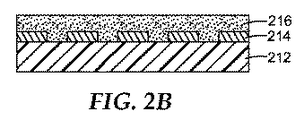
図2a及び2bは、提供される方法において有用な構成要素の概略図である。一実施形態では、透明電気活性基板(図2a)は、その上に透明金属酸化物層204(酸化インジウムスズ)が配置されたガラス基板202を有する。導電性基板(図2b)は、可撓性ポリマー基板212(いくつかの実施形態ではポリイミド)上に配置されたパターン化金属導電性素子214を有している。パターン化金属導電性素子214、及び基板の、パターン化金属導電性素子214によって覆われていない部分は、高誘電率接着複合材料216によって覆われている。
Figures 2a and 2b are schematic illustrations of components useful in the provided methods. In one embodiment, the transparent electroactive substrate (FIG. 2a) has a
図2cは、透明電気活性基板(図2a)が導電性基板(図2b)に積層された、提供される電子物品(エレクトロルミネセントランプ200)の一実施形態の概略図である。図2cに示される電子物品は、基板212上に配置されたパターン化金属導電性素子214を有している。高誘電率接着複合材料216は、導電性基板214及び蛍光体である電気活性層206と接触している。透明導体204(酸化インジウムスズ)が、蛍光体層206上に配置されている。透明導体204は、ガラス透明基板202上に配置されている。
FIG. 2c is a schematic diagram of one embodiment of the provided electronic article (electroluminescent lamp 200) in which a transparent electroactive substrate (FIG. 2a) is laminated to a conductive substrate (FIG. 2b). The electronic article shown in FIG. 2 c has a patterned metal
提供される物品及び方法は、電子装置に使用することができるディスプレイ装置に取り入れることができる。例示的な電子装置としては、アクチュエーター、人工筋肉及び臓器、スマート材料及び構造、微小電気機械(MEMS)装置、微小流体装置、音響装置、エレクトロルミネセントランプ、電子インク及びペーパー、電子リーダー、並びにセンサーが挙げられる。 The provided articles and methods can be incorporated into display devices that can be used in electronic devices. Exemplary electronic devices include actuators, artificial muscles and organs, smart materials and structures, microelectromechanical (MEMS) devices, microfluidic devices, acoustic devices, electroluminescent lamps, electronic ink and paper, electronic readers, and sensors. Is mentioned.
以下の実施例によって本発明の目的及び利点を更に説明するが、これらの実施例において記載される特定の材料及びその量、並びに他の条件及び詳細は、本発明を不要に限定するものとして解釈されるべきではない。 The following examples further illustrate the objects and advantages of the present invention, but the specific materials and amounts described in these examples, as well as other conditions and details, are to be construed as unnecessarily limiting the present invention. Should not be done.
コーティングされた粒子の調製
実施例において高誘電率充填剤として使用されるコーティングされた粒子は、最初に高導電性金属層でコーティングし、外側を導電層でコーティングしたグラスバブルズ/繊維/セラミックマイクロスフェアである。これらのコーティングを、それぞれの金属の物理的蒸着によって調製した。金属粒子及び炭素粒子などの他の充填剤を、物理的蒸着によって酸化アルミニウムなどの電気絶縁外層でコーティングすることによって、高誘電率充填剤を得た。
Preparation of Coated Particles Coated particles used as high dielectric constant fillers in the examples were first coated with a highly conductive metal layer and the outside was coated with a conductive layer on a glass bubbles / fiber / ceramic micro. It is a sphere. These coatings were prepared by physical vapor deposition of the respective metal. High dielectric constant fillers were obtained by coating other fillers such as metal particles and carbon particles with an electrically insulating outer layer such as aluminum oxide by physical vapor deposition.
物理的蒸着(PVD)プロセスを行うための装置310を図3a及び3bに示す。装置310は、粒子攪拌器316を収容した真空チャンバ314を画定するハウジング312を有している。必要に応じてアルミニウム合金で形成することができるハウジング312は、垂直な向きに配置された中空の円筒である(高さ45cm、直径50cm)。基部318は、高真空ゲートバルブ322用のポート320を有しており、ポート320に続いて15cmの拡散ポンプ324、及び粒子攪拌器316の支持部326が配されている。チャンバ314は、10−6torr(0.13mPa)の範囲のバックグラウンド圧にまで脱気することができる。
An
ハウジング312の上部は、直流マグネトロンスパッター蒸着ソース330(US Gun II、ユー・エス社(US,INC)(カリフォルニア州サンホセ))用の外部マウントが取り付けられた、取り外し可能なゴム製Lガスケットで封止されたプレート328を有している。ソース330内には、金属スパッターターゲット332(13cm×20cm、厚さ1.25cm)が固定されている。スパッターソース330は、アーク抑制式Sparc−le 20(アドバンスド・エナジー・インダストリーズ社(Advanced Energy Industries,Inc)(コロラド州、フォートコリンズ))が取り付けられたMDX−10 Magnetron Drive(アドバンスドエナジーインダストリーズ社(Advanced Energy Industries,Inc)(コロラド州、フォートコリンズ))によって作動される。
The top of the
粒子撹拌器316は、上部336に四角形の開口部34(16.5cm×13.5cm)が設けられた中空の円筒(長さ24cm×直径19cm、水平)である。開口部334はスパッターターゲット332の表面336の真下、7cmの位置に配置されているため、スパッタリングされた金属原子は攪拌器容積338に入ることができる。攪拌器316は、シャフト340にその軸と整列させて取り付けられている。シャフト340は四角形の断面を有しており、これに4枚の四角形のブレード342がボルト固定されて、支持粒子を攪拌するための攪拌機構又はパドルを形成している。ブレード342はそれぞれ、ブレード342と攪拌器の円筒体316とによって形成される4つの区画のそれぞれに含まれる粒子体積間の連通を促すための2個の穴344を有している。この粒子攪拌器は、最大で2000cm3の体積のグラスバブルズ又は他の基材を収容することができる。この装置の典型的な使用の態様を下記実施例に述べる。
The
粉末電気抵抗率試験
コーティングされた粒子の体積電気抵抗率を、社内製の試験セルを使用して測定した。試験セルは、断面積が1.0cm2の円筒状の空洞を有するDERLINブロックからなるものを用いた。空洞の底を真鍮電極で覆った。他方の電極は、断面積が1.0cm2の真鍮円筒体とし、これを空洞内に嵌め込んだ。試験するコーティングされた粒子を、底部電極から1.0cmの高さにまで空洞内に満たした。次に、真鍮円筒体を挿入し、粉末に作用する全体の圧力が18psi(124kPa)となるように真鍮円筒体の上に重りを載せた。電極をデジタルマルチメータに接続して抵抗を測定した。この構成によれば、測定される抵抗は粒子の体積抵抗率に相当することになる。
Powder electrical resistivity test The volume electrical resistivity of the coated particles was measured using an in-house test cell. The test cell used was a DERLIN block having a cylindrical cavity having a cross-sectional area of 1.0 cm 2 . The bottom of the cavity was covered with a brass electrode. The other electrode was a brass cylinder having a cross-sectional area of 1.0 cm 2 and was fitted into the cavity. The coated particles to be tested were filled into the cavity to a height of 1.0 cm from the bottom electrode. Next, a brass cylinder was inserted and a weight was placed on the brass cylinder so that the total pressure acting on the powder was 18 psi (124 kPa). The resistance was measured by connecting the electrode to a digital multimeter. According to this configuration, the measured resistance corresponds to the volume resistivity of the particles.
コーティングされた粒子を含む複合材料 Composite material containing coated particles
ポリエチレン複合材料
コーティングされた粒子を、160℃の温度に維持したBrabenderバッチミキサー中でポリマー溶融物(ポリエチレン、ENGAGE 8200、ダウ社(Dow))に加えた。2種類の材料を、約15〜20分間、65rpmでブレードを回転させることによって互いに混合することによって、複合材料を形成した。溶融した複合材料を、最初に2枚のポリエステルライナーの間に置いて3層のサンドウィッチ構造とすることによって、複合材料の平板なフィルムを形成した。次に、このサンドウィッチ構造を2枚のアルミニウムプレートの間に置いた。次にこのアセンブリ全体を、加熱したCarver labプレス(モデル2518、フレッド・エス・カーバー社(Fred S.Carver Co.)(インディアナ州ワバシュ))に挿入し、1000psi(6900kPa)の圧力及び150℃の温度で平板なフィルムに成形した。アルミニウムプレート間にシムを挿入して各試料の厚さを調節した。複合材料の各フィルムは、直径約18cm及び厚さ1.0〜1.5mmであった。
Polyethylene composite The coated particles were added to the polymer melt (polyethylene, ENGAGE 8200, Dow) in a Brabender batch mixer maintained at a temperature of 160 ° C. The two materials were mixed together by rotating the blades at 65 rpm for about 15-20 minutes to form a composite material. The molten composite material was first placed between two polyester liners to form a three-layer sandwich structure, thereby forming a flat film of the composite material. Next, this sandwich structure was placed between two aluminum plates. The entire assembly is then inserted into a heated Carver lab press (model 2518, Fred S. Carver Co., Wabash, Ind.) At a pressure of 1000 psi (6900 kPa) and 150 ° C. Molded into a flat film at temperature. Shims were inserted between aluminum plates to adjust the thickness of each sample. Each film of composite material was about 18 cm in diameter and 1.0-1.5 mm thick.
エポキシ複合材料
2液型DEVCON 5 Minuteエポキシ(デブコン社(Devcon)、マサチューセッツ州ダンバース)を使用して、エポキシ複合材料を調製した。既知の重量のコーティングされた粒子と2液型エポキシとを、プラスチックビーカー中でスパチュラでよく混合した。2分後、アルミニウムプレート上に置かれた剥離ライナー上に混合物を注いだ。この混合物及びアルミニウムプレートの上に別の剥離ライナーを置いた。シムを挿入して所望の厚さとした。次にこのサンドウィッチアセンブリを、室温に維持したCarver labプレスに挿入した。5000psi(35MPa)の圧力を加え、最低で1時間維持した。
Epoxy Composites Epoxy composites were prepared using a two-part DEVCON 5 Minute epoxy (Devcon, Danvers, Mass.). A known weight of coated particles and two-part epoxy were mixed well with a spatula in a plastic beaker. After 2 minutes, the mixture was poured onto a release liner placed on an aluminum plate. Another release liner was placed over the mixture and aluminum plate. Shims were inserted to achieve the desired thickness. The sandwich assembly was then inserted into a Carver lab press maintained at room temperature. A pressure of 5000 psi (35 MPa) was applied and maintained for a minimum of 1 hour.
各複合材料は、直径10cm及び厚さ1.5〜2.0mmであった。 Each composite material had a diameter of 10 cm and a thickness of 1.5 to 2.0 mm.
誘電率の測定(実施例1〜5に使用)
各複合材料の誘電特性を、1kHz以下の低周波数でLCRメーター(モデル72−960、テンマ社(TENMA)、オハイオ州センタービル)を用いて、室温(23℃)で測定した。底部電極は、直径10cmのアルミニウムプレートとした。上部電極は、直径4cmのアルミニウムプレートとした。プレートの厚さは1.4cmであった。底部電極をLCRメーターのマイナス端子に接続し、上部電極をプラス端子に接続した。平板な各複合材料試料を電極間に置いた。18psi(124kPa)の力に相当する重りを上部電極の上に載せて、各電極と試料表面とを密着させた。測定された静電容量(ピコファラデー(pF))を用い、下式を用いて複合材料の誘電率(k)を計算した。
K=C×d/e0×A
式中、Cは、静電容量をpFで測定した値であり、dは、スラブの厚さをmで測定した値であり、Aは、上部電極の断面積=50cm2=5×10⁻³m2であり、e0=8.85×10⁻¹²F/mである。
Measurement of dielectric constant (used in Examples 1-5)
The dielectric properties of each composite material were measured at room temperature (23 ° C.) using an LCR meter (Model 72-960, TENMA, Centerville, Ohio) at a low frequency of 1 kHz or less. The bottom electrode was an aluminum plate with a diameter of 10 cm. The upper electrode was an aluminum plate with a diameter of 4 cm. The plate thickness was 1.4 cm. The bottom electrode was connected to the negative terminal of the LCR meter and the top electrode was connected to the positive terminal. Each flat composite sample was placed between the electrodes. A weight corresponding to a force of 18 psi (124 kPa) was placed on the upper electrode to bring each electrode into close contact with the sample surface. Using the measured capacitance (picofaraday (pF)), the dielectric constant (k) of the composite material was calculated using the following equation.
K = C × d / e 0 × A
In the formula, C is a value obtained by measuring the capacitance in pF, d is a value obtained by measuring the thickness of the slab in m, and A is a cross-sectional area of the upper electrode = 50 cm 2 = 5 × 10 − 3 m 2 and e 0 = 8.85 × 10 −12 F / m.
実施例1及び比較例
市販の高誘電率(k)充填剤を比較例において使用した。BaTiO3は、約1200の極めて高い誘電率を示す。BaTiO3は、フェロ社(Ferro Corporation)(オハイオ州クリーブランド)より購入した。638.46gのスリー・エム社(3M)製SCOTCHLITE S60グラスバブルズを粒子攪拌器に装填し、スパッター蒸着によってグラスバブルズをアルミニウムでコーティングした。標的には3kWの出力を加えて、コーティングを24時間行った。チャンバを空気でベントし、試料の小部分(10cm3)を取り出して粉末抵抗率を測定した。3.5ω・cmの抵抗率が得られた。チャンバを通じた3.0sccmの流れを用い、部分酸素雰囲気下でアルミニウムの反応性スパッター蒸着によって外側絶縁層を塗布した。3kWの出力を8時間加えて、絶縁層を形成した。チャンバをベントし、粒子を取り出した。測定された粉末抵抗率は30メガオーム/cmであった。
Example 1 and Comparative Example Commercially available high dielectric constant (k) fillers were used in the comparative examples. BaTiO 3 exhibits a very high dielectric constant of about 1200. BaTiO 3 was purchased from Ferro Corporation (Cleveland, Ohio). 638.46 g of SCOTCHLITE S60 glass bubbles from 3M (3M) was loaded into a particle stirrer and the glass bubbles were coated with aluminum by sputter deposition. The target was applied with a power of 3 kW and coated for 24 hours. The chamber was vented with air and a small portion (10 cm 3 ) of the sample was removed and the powder resistivity was measured. A resistivity of 3.5 Ω · cm was obtained. The outer insulating layer was applied by reactive sputter deposition of aluminum under a partial oxygen atmosphere using a flow of 3.0 sccm through the chamber. An insulating layer was formed by applying an output of 3 kW for 8 hours. The chamber was vented and the particles were removed. The measured powder resistivity was 30 megohm / cm.
10、20、30、40及び50体積%の充填剤濃度で、エポキシ複合材料を調製した。誘電率の値を測定し、下記表1に示した。

(実施例2)
異なるサイズのスリー・エム社(3M)製グラスバブルズ上に金属及び金属酸化物コーティングを物理的蒸着することによって、以下の充填剤を調製した。各複合材料はポリエチレン基質中で調製し、誘電率の値を下記表2に示した。
The following fillers were prepared by physical vapor deposition of metal and metal oxide coatings on 3M glass bubbles of different sizes (3M). Each composite material was prepared in a polyethylene substrate, and the dielectric constant values are shown in Table 2 below.
(実施例3)
RCF 600ガラス薄片を、エヌ・ジー・エフ・カナダ社(NGF Canada)より購入した。ガラス薄片にタングステンをコーティングした後、酸化アルミニウム絶縁層をコーティングして高誘電率充填剤を調製した。409.64gのRCF−600ガラス薄片を粒子攪拌器に装填し、タングステン金属ターゲットを使用して最初にタングステンでコーティングした。3.00kWの陰極出力を9時間加えた。コーティングの後、上記の粉末抵抗率装置を使用して、充填剤の抵抗率を確認した。抵抗率を測定したところ1.0ω・cmであった。アルミニウムスパッター標的を使用して、外側絶縁AlOx層を蒸着した。スパッターチャンバ内において部分酸素雰囲気下で、2.00kWの陰極出力を7時間加えた。5.0sccmの酸素流をアルゴンとともにチャンバに導入した。スパッタープロセスの圧力は、10mtorr(1.33Pa)に維持した。充填剤は、Mω・cm(メガオーム・センチメートル)の範囲の粉末抵抗率を示した。各複合材料はポリエチレン中で調製し、誘電率の値を下記表3に示した。
RCF 600 glass flakes were purchased from NGF Canada. After coating the glass flakes with tungsten, an aluminum oxide insulating layer was coated to prepare a high dielectric constant filler. 409.64 g of RCF-600 glass flakes were loaded into a particle stirrer and first coated with tungsten using a tungsten metal target. A 3.00 kW cathode power was applied for 9 hours. After coating, the filler resistivity was checked using the powder resistivity apparatus described above. The resistivity was measured and found to be 1.0 Ω · cm. An outer insulating AlO x layer was deposited using an aluminum sputter target. A 2.00 kW cathode power was applied for 7 hours under a partial oxygen atmosphere in a sputter chamber. A 5.0 sccm oxygen flow was introduced into the chamber along with argon. The pressure of the sputter process was maintained at 10 mtorr (1.33 Pa). The filler exhibited a powder resistivity in the range of Mω · cm (mega ohm · centimeter). Each composite material was prepared in polyethylene, and the dielectric constant values are shown in Table 3 below.
(実施例4)
AlOx絶縁層を、キャボット社(Cabot)のVulcanカーボンブラック(XC72R)上にスパッター蒸着した。誘電率の値を測定し、コーティングしていないカーボンブラックとの比較を表4に示した。高い損失正接の値は、コーティングしていないカーボンブラックが損失を生じやすい材料であることを示している(高い誘電損失)。
An AlOx insulating layer was sputter deposited onto Vulcan carbon black (XC72R) from Cabot. The dielectric constant values were measured, and a comparison with uncoated carbon black is shown in Table 4. A high loss tangent value indicates that uncoated carbon black is a loss-prone material (high dielectric loss).
(実施例5)
アルミニウム粉末(1〜3マイクロメートル)をアトランティック・イクイップメント・エンジニアズ社(Atlantic Equipment Engineers)(ニュージャージー州バーゲンフィールド)より購入した。絶縁AlOx層を反応性スパッタリングによって蒸着した。誘電率及び損失正接(括弧内)の値を表5に示す。
Aluminum powder (1-3 micrometers) was purchased from Atlantic Equipment Engineers (Bargainfield, NJ). An insulating AlOx layer was deposited by reactive sputtering. Table 5 shows values of dielectric constant and loss tangent (in parentheses).
実施例6の試験方法
剥離力試験
接着フィルムの試料を、1インチ(2.54cm)のゴムローラー及び約0.35kg/平方cmの手の圧力で、厚さ45μmのポリエチレンテレフタレート(PET)フィルムに積層した。この接着フィルム/PETの積層体から、幅1インチ(2.54cm)のストリップを切り取った。この試験ストリップの接着フィルム側を、アセトンで1回、ヘプタンで3回拭くことによって予めきれいにしたステンレス鋼プレートに、2kgのゴムローラーで積層した。積層した試験試料を周囲条件下に1時間置いた。接着フィルム試料/PET試験試料を、180°の角度で毎分30.5cmの速度でステンレス鋼の表面から剥離した。その力を、ImassモデルSP−2000試験機(アイマス社(Imass Inc.)、バージニア州アコード)によって測定した。
Test Method of Example 6 Peel Force Test An adhesive film sample was applied to a 45 μm thick polyethylene terephthalate (PET) film with a 1 inch (2.54 cm) rubber roller and a hand pressure of about 0.35 kg / square cm. Laminated. A 1 inch wide (2.54 cm) strip was cut from the adhesive film / PET laminate. The adhesive film side of the test strip was laminated with a 2 kg rubber roller onto a stainless steel plate previously cleaned by wiping once with acetone and three times with heptane. The laminated test sample was placed under ambient conditions for 1 hour. The adhesive film sample / PET test sample was peeled from the surface of the stainless steel at a rate of 30.5 cm per minute at an angle of 180 °. The force was measured with an Imass model SP-2000 tester (Imass Inc., Accord, VA).
誘電特性を測定するための方法(実施例6)
試料の形態:厚さ約1mm、直径40mmのフィルム又は薄いシート液体材料については、特殊な液体セル、スペーサーで隔離された金属電極又はくし形電極が利用可能である。
Method for measuring dielectric properties (Example 6)
Sample form: For a film or thin sheet liquid material about 1 mm thick and 40 mm in diameter, special liquid cells, metal electrodes separated by spacers or comb electrodes can be used.
この測定では、平行プレート電極の形態を選択した。直流導電率の通常の直接測定法は、これらのゲル試料は取り扱いが困難であるために適用できなかった。 For this measurement, a parallel plate electrode configuration was selected. The usual direct measurement method of DC conductivity could not be applied because these gel samples are difficult to handle.
誘電率の測定値は、平行プレート電極及びAndeen Hagerling 2500A 1kHz超高精度静電容量ブリッジを使用し、「固体電気絶縁の交流損失特性及び誘電率(誘電定数)の標準的試験法(Standard Test Methods for AC Loss Characteristics and Permittivity(Dielectric Constant) of Solid Electrical Insulation)」と題するASTM D150に従って得た。各接着剤試料を、試料中に気泡が生じないように注意しながら、目標とする全体の厚さ(約1.8〜1.9mm)にまで注意深く積層した。積層した接着剤試料を、直径40mm、厚さ2mmの2枚の研磨した真鍮製ディスクの間に挿入した。次に、この真鍮電極で試料を挟んだアセンブリを、平行プレート試料コンデンサと、Andeen Hagerling 2500A 1kHz超高精度静電容量ブリッジとの間の界面を形成するために、Mopsik固定具に挿入した。各コンデンサの有限サイズによって生じる漏れ磁場の静電容量を説明するため、各測定にわずかな補正を適用した。 The measured value of the dielectric constant was measured using a parallel plate electrode and an Anden Hagering 2500A 1 kHz ultra-high-accuracy capacitance bridge, and “Standard Test Methods for AC Loss Characteristics and Dielectric Constant (Dielectric Constant) of Solid Electrical Insulation” for AC Loss Characteristics and Permittivity (Dielectric Constant) of Solid Electrical Insulation) ”. Each adhesive sample was carefully laminated to the target total thickness (about 1.8-1.9 mm), taking care not to generate bubbles in the sample. The laminated adhesive sample was inserted between two polished brass disks having a diameter of 40 mm and a thickness of 2 mm. This brass electrode assembly was then inserted into a Mopsik fixture to form an interface between the parallel plate sample capacitor and the Andene Hagerling 2500A 1 kHz ultra-precision capacitance bridge. A slight correction was applied to each measurement to account for the stray field capacitance caused by the finite size of each capacitor.
試料の誘電率及び直流導電率を、Novocontrol高温広帯域誘電分光計(0.01〜10MHz)により、平行プレートの形態(上記の写真を参照)で測定した。直流導電率は、周波数に対する仮想誘電率データ(誘電損失)を、直流導電機構と同時に作動する単一の誘電緩和プロセスに対してフィッティングすることによる低周波数での外挿から得ることができる。この多変量フィッティングを用いることで、本発明者らは、低周波数での誘電緩和機構の残留効果が導電率から確実に取り除かれるようにすることができた。テフロン及びPMMAで得られた結果は、文献においてこれまでに報告されている内容とよく一致している。正確と考えられるこの導電率の測定法の最大の分解能は、約e−17S/cmである。 The dielectric constant and direct current conductivity of the sample were measured in the form of parallel plates (see the above picture) with a Novocontrol high temperature broadband dielectric spectrometer (0.01-10 MHz). DC conductivity can be obtained from low frequency extrapolation by fitting virtual dielectric constant data (dielectric loss) versus frequency to a single dielectric relaxation process operating simultaneously with the DC conduction mechanism. By using this multivariate fitting, we were able to ensure that the residual effects of the dielectric relaxation mechanism at low frequencies were removed from the conductivity. The results obtained with Teflon and PMMA are in good agreement with what has been reported so far in the literature. The maximum resolution of this conductivity measurement considered accurate is about e -17 S / cm.
(実施例6A〜6D)
誘電性充填剤Aの調製
詳細な説明において述べられ、図1及び2に示される装置を以下のように使用して、誘電性充填剤Aを調製した。スリー・エム社(3M)製S60グラスバブルズの粒径は15〜65マイクロメートルの範囲であり、中央値は30マイクロメートルである。1400cc(430g)のS60 SCOTCHLITEグラスバブルズ粒子を、対流式オーブン中、150℃で6時間乾燥させた。乾燥した粒子を粒子攪拌装置10に入れ、チャンバ14を脱気した。チャンバ圧が10−5torr(1.33mPa)の範囲となった時点で、アルゴンスパッタリングガスをチャンバ14に約10mtorr(1.33Pa)の圧力で導入した。金属アルミニウムをスパッターターゲットとして使用した。次に、2.50kWの陰極出力を加えることによって蒸着プロセスを開始した。アルミニウム蒸着プロセスの間、粒子攪拌器のシャフト40を約4rpmで回転させた。20時間後に出力を停止した。アルゴンスパッターガスに加えて、酸素ガスを5sccm(1分当たりの標準立方cm)の速度で導入することにより、AlOx層をその上にコーティングした。全体の圧力を10mtorr(1.33Pa)に維持した。4rpmで粒子を攪拌しながら、2.00kWの陰極出力を18時間加えた。18時間の終了時点でチャンバを周囲条件にまでベントし、攪拌器から粒子を取り出した。アルミニウムコーティングしたS60グラスバブルズの粉末抵抗率は2ω・cmよりも低く、最終的なコーティングの粉末抵抗率は、Mω・cm(メガオーム・cm)の範囲であった。
(Examples 6A to 6D)
Preparation of Dielectric Filler A Dielectric Filler A was prepared using the apparatus described in the detailed description and shown in FIGS. 1 and 2 as follows. The particle size of S60 Glass Bubbles manufactured by 3M (3M) is in the range of 15 to 65 micrometers, and the median is 30 micrometers. 1400 cc (430 g) of S60 SCOTCHLITE glass bubbles particles were dried at 150 ° C. for 6 hours in a convection oven. The dried particles were placed in the particle agitator 10 and the chamber 14 was evacuated. When the chamber pressure was in the range of 10 −5 torr (1.33 mPa), argon sputtering gas was introduced into the chamber 14 at a pressure of about 10 mtorr (1.33 Pa). Metal aluminum was used as a sputtering target. The deposition process was then started by applying a 2.50 kW cathode power. During the aluminum deposition process, the particle agitator shaft 40 was rotated at about 4 rpm. The output was stopped after 20 hours. In addition to the argon sputter gas, an AlO x layer was coated thereon by introducing oxygen gas at a rate of 5 sccm (standard cubic cm per minute). The total pressure was maintained at 10 mtorr (1.33 Pa). While stirring the particles at 4 rpm, a cathode output of 2.00 kW was applied for 18 hours. At the end of 18 hours, the chamber was vented to ambient conditions and the particles were removed from the agitator. The powder resistivity of the aluminum coated S60 glass bubbles was lower than 2 Ω · cm, and the powder resistivity of the final coating was in the range of MΩ · cm (mega ohm · cm).
誘電性充填剤Bの調製
誘電性充填剤Bの調製法
詳細な説明において述べられ、図1及び2に示される装置を以下のように使用して、以下の手順に従って誘電性充填剤Bを調製した。iM30K SCOTCHLITEグラスバブルズ(スリー・エム社(3M Company)、ミネソタ州セントポール)は、18マイクロメートルの平均粒径を有する。503.95gのiM30K SCOTCHLITEグラスバブルズ粒子を、対流式オーブン中、150℃で6時間乾燥させた。乾燥した粒子を粒子攪拌装置10に入れ、チャンバ14を脱気した。チャンバ圧が10−5torr(1.33mPa)の範囲となった時点で、アルゴンスパッタリングガスをチャンバ14に約10mtorr(1.33Pa)の圧力で導入した。四角形の金属タングステンをスパッターターゲットとして使用した。次に、3.00kWの陰極出力を加えることによって蒸着プロセスを開始した。タングステン蒸着プロセスの間、粒子攪拌器のシャフト40を約4rpmで回転させた。13時間後に出力を停止した。タングステンコーティングしたグラスバブルズの粉末抵抗率は0.6ω・cmであった。アルゴンスパッターガスに加えて、酸素ガスを5sccm(1分当たりの標準立方cm)の速度で導入することにより、AlOx層をその上にコーティングした。全体の圧力を10mtorr(1.33Pa)に維持した。4rpmで粒子を攪拌しながら、2.00kWの陰極出力を7時間加えた。7時間の終了時点でチャンバを周囲条件にまでベントし、攪拌器から粒子を取り出した。最終的なコーティングの粉末抵抗率は、Mω・cm(メガオーム・cm)の範囲であった。
Preparation of Dielectric Filler B Method of Preparing Dielectric Filler B Prepare dielectric filler B according to the following procedure using the apparatus described in the detailed description and shown in FIGS. 1 and 2 as follows: did. iM30K SCOTCHLITE Glass Bubbles (3M Company, St. Paul, Minn.) has an average particle size of 18 micrometers. 503.95 g of iM30K SCOTCHLITE glass bubbles particles were dried in a convection oven at 150 ° C. for 6 hours. The dried particles were placed in the particle agitator 10 and the chamber 14 was evacuated. When the chamber pressure was in the range of 10 −5 torr (1.33 mPa), argon sputtering gas was introduced into the chamber 14 at a pressure of about 10 mtorr (1.33 Pa). Square metal tungsten was used as a sputtering target. The deposition process was then started by applying a 3.00 kW cathode power. During the tungsten deposition process, the particle agitator shaft 40 was rotated at about 4 rpm. The output was stopped after 13 hours. The powder resistivity of glass bubbles coated with tungsten was 0.6 Ω · cm. In addition to the argon sputter gas, an AlOx layer was coated thereon by introducing oxygen gas at a rate of 5 sccm (standard cubic cm per minute). The total pressure was maintained at 10 mtorr (1.33 Pa). While stirring the particles at 4 rpm, a cathode output of 2.00 kW was applied for 7 hours. At the end of 7 hours, the chamber was vented to ambient conditions and the particles were removed from the agitator. The powder resistivity of the final coating was in the range of Mω · cm (mega ohm · cm).
シロップA−80% N−ビニルピロリドンと20%アクリルアミド(重量基準)の混合物を互いに混合して、NVP/アクリルアミド混合物を形成した。10重量%(wt%)のこの混合物、16.99重量%の更なるN−ビニルピロリドン、及び72.97重量%のイソオクチルアクリレートを、0.04重量%のIRGACURE 651と混合した。この混合物を部分重合させて、米国特許第6,339,111号(ムーン(Moon)ら)に教示されるようなシロップを形成した。部分重合させたシロップの重量に対して、更なるIRGACURE 651(0.369重量%)及び0.149重量%の1,6−ヘキサンジオールジアクリレート(HDDA)を部分重合させたシロップに加えてシロップAを形成した。 A mixture of syrup A-80% N-vinylpyrrolidone and 20% acrylamide (by weight) was mixed together to form an NVP / acrylamide mixture. 10 wt% (wt%) of this mixture, 16.99 wt% of additional N-vinyl pyrrolidone, and 72.97 wt% of isooctyl acrylate were mixed with 0.04 wt% of IRGACURE 651. This mixture was partially polymerized to form a syrup as taught in US Pat. No. 6,339,111 (Moon et al.). Additional IRGACURE 651 (0.369 wt%) and 0.149 wt% 1,6-hexanediol diacrylate (HDDA) to the partially polymerized syrup, based on the weight of the partially polymerized syrup, added to the syrup A was formed.
(実施例6A〜6D)
実施例6A−誘電性充填剤A(充填率20重量%)を含む複合材料。
500mLのプラスチック製ビーカーに、240gのシロップAと60gの誘電性充填剤Aとを入れた。次に材料を標準的な実験用ブレードミキサーを用いて混合した後、減圧下で5分間脱気した。次に材料を、1.5ミル(38μm)のシー・ピー・フィルムズ社(CPFilms)製T−10ライナーと、2ミル(50.8μm)のシー・ピー・フィルムズ社(CPFilms)製T−30ライナーとの間に、13フィート/分(4m/分)の速度で、2ミル(50.8μm)の厚さにコーティングした。接着剤コーティングの表面において受容されるエネルギーが約270mJ/cm2となるように、コーティングに蛍光ブラックライトランプを照射した。この材料の誘電率は、1kHzにおいて7.19であった。2.0ミル(50.8μm)の接着剤同士を積層して厚さ2mmの試料を形成することにより、誘電率試験試料を調製した。
(Examples 6A to 6D)
Example 6A—Composite material containing dielectric filler A (20 wt% loading).
In a 500 mL plastic beaker, 240 g of syrup A and 60 g of dielectric filler A were placed. The material was then mixed using a standard laboratory blade mixer and then degassed under reduced pressure for 5 minutes. The materials were then made into 1.5 mil (38 μm) CP Films T-10 liner and 2 mil (50.8 μm) CP Films T-30. Coated between the liners at a speed of 13 ft / min (4 m / min) to a thickness of 2 mils (50.8 μm). The coating was irradiated with a fluorescent black light lamp so that the energy received at the surface of the adhesive coating was about 270 mJ / cm 2 . The dielectric constant of this material was 7.19 at 1 kHz. A dielectric constant test sample was prepared by laminating 2.0 mil (50.8 μm) adhesives to form a 2 mm thick sample.
実施例6B−誘電性充填剤A(充填率30重量%)を含む複合材料。
500mLのプラスチック製ビーカーに、210gのシロップAと90gの誘電性充填剤Aとを入れた。次に材料を標準的な実験用ブレードミキサーを用いて混合した後、5分間脱気した。次に、材料を13フィート/分(4m/分)の速度で、2.0ミル(50.8μm)の厚さに、間にコーティングした。接着剤コーティングの表面において受容されるエネルギーが約270mJ/cm2となるように、コーティングに蛍光ブラックライトランプを照射した。この材料の誘電率は、1kHzにおいて15.71であった。2.0ミル(50.8μm)の接着剤同士を積層して厚さ2mmの試料を形成することにより、誘電率試験試料を調製した。
Example 6B—Composite material containing dielectric filler A (filling 30% by weight).
In a 500 mL plastic beaker, 210 g syrup A and 90 g dielectric filler A were placed. The material was then mixed using a standard laboratory blade mixer and degassed for 5 minutes. The material was then coated in-between to a thickness of 2.0 mils (50.8 μm) at a speed of 13 feet / min (4 m / min). The coating was irradiated with a fluorescent black light lamp so that the energy received at the surface of the adhesive coating was about 270 mJ / cm 2 . The dielectric constant of this material was 15.71 at 1 kHz. A dielectric constant test sample was prepared by laminating 2.0 mil (50.8 μm) adhesives to form a 2 mm thick sample.
実施例6C−誘電性充填剤B(充填率25重量%)を含む複合材料。
1ガロン(3.78リットル)の容器に、487.5gのシロップA、368.55gのイソオクチルアクリレート、118.95gのN−ビニルピロリドン、及び325gの誘電性充填剤Bを入れた。材料を標準的な実験用ブレードミキサーを用いて混合した後、減圧下で15分間脱気した。次にこの溶液を、1.5ミル(38μm)のシー・ピー・フィルムズ社(CPFilms)製T−10ライナーと、2ミル(50.8μm)のシー・ピー・フィルムズ社(CPFilms)製T−30ライナーとの間に、15フィート/分(4.5m/分)の速度で、0.9ミル(23μm)の厚さにコーティングした。次に接着剤コーティングの表面において受容されるエネルギーが約270mJ/cm2となるように、コーティングに蛍光ブラックライトランプを照射した。この材料の誘電率は、1kHzにおいて9.68であった。0.9ミル(23μm)の接着剤同士を積層して厚さ1mmの試料を形成することにより、誘電率試験試料を調製した。
Example 6C—Composite material containing dielectric filler B (filling factor 25% by weight).
A 1 gallon (3.78 liter) container was charged with 487.5 g syrup A, 368.55 g isooctyl acrylate, 118.95 g N-vinylpyrrolidone, and 325 g dielectric filler B. The material was mixed using a standard laboratory blade mixer and then degassed for 15 minutes under reduced pressure. This solution was then added to a 1.5 mil (38 μm) CP Films T-10 liner and a 2 mil (50.8 μm) CP Films T-10 liner. Coated between 30 liners at a rate of 15 feet / minute (4.5 m / minute) to a thickness of 0.9 mil (23 μm). The coating was then irradiated with a fluorescent black light lamp so that the energy received at the surface of the adhesive coating was about 270 mJ / cm 2 . The dielectric constant of this material was 9.68 at 1 kHz. A dielectric constant test sample was prepared by laminating 0.9 mil (23 μm) adhesives to form a 1 mm thick sample.
実施例6D−誘電性充填剤B(充填率35重量%)を含む複合材料。
1リットルの容器に、92.87gのシロップA、70.20gのイソオクチルアクリレート、22.66gのN−ビニルピロリドン、及び100gの誘電性充填剤Bを入れた。材料を標準的な実験用ブレードミキサーを用いて混合した後、減圧下で15分間脱気した。次にこの溶液を、1.5ミル(38μm)のシー・ピー・フィルムズ社(CPFilms)製T−10ライナーと、2ミル(50.8μm)のシー・ピー・フィルムズ社(CPFilms)製T−30ライナーとの間に、15フィート/分(4.5m/分)の速度で、0.9ミル(23μm)の厚さにコーティングした。次に接着剤コーティングの表面において受容されるエネルギーが約270mJ/cm2となるように、コーティングに蛍光ブラックライトランプを照射した。この材料の誘電率は、1kHzにおいて15.00であった。0.9ミル(23μm)の接着剤同士を積層して厚さ1mmの試料を形成することにより、誘電率試験試料を調製した。
Example 6D—Composite material containing dielectric filler B (filling 35% by weight).
In a 1 liter container, 92.87 g syrup A, 70.20 g isooctyl acrylate, 22.66 g N-vinylpyrrolidone, and 100 g dielectric filler B were placed. The material was mixed using a standard laboratory blade mixer and then degassed for 15 minutes under reduced pressure. This solution was then added to a 1.5 mil (38 μm) CP Films T-10 liner and a 2 mil (50.8 μm) CP Films T-10 liner. Coated between 30 liners at a rate of 15 feet / minute (4.5 m / minute) to a thickness of 0.9 mil (23 μm). The coating was then irradiated with a fluorescent black light lamp so that the energy received at the surface of the adhesive coating was about 270 mJ / cm 2 . The dielectric constant of this material was 15.00 at 1 kHz. A dielectric constant test sample was prepared by laminating 0.9 mil (23 μm) adhesives to form a 1 mm thick sample.
剥離接着力
剥離接着力(180°)を、実施例6A〜6Dで調製した接着剤で測定し、このデータを下記表に示す。幅1インチ(2.54cm)の接着剤試料を、幅1インチ(2.54cm)/厚さ2ミル(51μm)のアルミニウム箔と、幅2インチ(5.08cm)/厚さ1.23mmのステンレス鋼試験プレートとの間に接着した。試験試料の調製後、試料の調製と180°剥離試験との間に1時間のドウェル時間をおいた。180°剥離試験を、12インチ(30.5cm)/分で、2秒間のデータ収集遅延時間の後に10秒間のデータ収集時間を取って行った。「フェース面」(FS)及び「裏面」(BS)の両方の接着力試験を行った。接着剤の「フェース面」は、「最も容易に剥離できる」ライナーを剥離した際に露出する接着剤の面とした。接着剤の「裏面」は、「フェース面」に対して反対側の面とした。180°剥離試験は、「フェース面」(FS)及び「裏面」(BS)の両方がステンレス鋼プレートに接着した状態で行った。最後に、180°剥離試験後にステンレス鋼プレートに接着したまま残留した接着剤の比率(%)として「転写率(%)」を記録した。結果を下記表6に示す。
表6のデータは、1kHzにおいて約7〜16の高い誘電率を有する実施例6A〜6Dの複合材料は、相当の剥離強度も有し、高誘電率接着複合材料として有用でありうることを示すものである。 The data in Table 6 shows that the composites of Examples 6A-6D having a high dielectric constant of about 7-16 at 1 kHz also have considerable peel strength and can be useful as high dielectric constant adhesive composites. Is.
本発明の範囲及び趣旨から逸脱することなく本発明に様々な変更及び改変を行いうる点は、当業者には明らかであろう。本発明は、本明細書で述べる例示的な実施形態及び実施例によって不要に限定されない点、また、こうした実施例及び実施形態はあくまで例として与えられるものであり、本発明の範囲は、本明細書において以下に記載される「特許請求の範囲」によってのみ限定されるものである点は理解すべきである。本開示に引用される参照文献はすべて、その全体を本明細書に援用するものである。 It will be apparent to those skilled in the art that various modifications and variations can be made to the present invention without departing from the scope and spirit of the invention. The present invention is not unnecessarily limited by the exemplary embodiments and examples described herein, and these examples and embodiments are given by way of example only, and the scope of the present invention is defined by this specification. It should be understood that the invention is limited only by the claims set forth below. All references cited in this disclosure are hereby incorporated by reference in their entirety.
Claims (3)
基板と、
前記基板に隣接した導電性素子と、
第1の表面及び第2の表面を有し、前記第1の表面が前記導電性素子の少なくとも一部に隣接した、高誘電率複合材料と、
前記高誘電率複合材料の前記第2の表面の少なくとも一部に隣接する蛍光体層と、を備え、
前記高誘電率複合材料が、
ポリマー結合剤と、
前記結合剤中に保持された1〜80体積%の粒子状充填剤と、を含み、
前記充填剤が、
中空のコア本体と、
前記中空のコア本体を実質的に包囲する導電層と、
前記導電層を実質的に包囲する絶縁層と、を含む粒子を含み、
前記絶縁層が、酸化アルミニウムからなり、
前記蛍光体層が、前記導電性素子と電気的に導通している、電子物品。 Electronic goods,
A substrate,
A conductive element adjacent to the substrate;
A high dielectric constant composite material having a first surface and a second surface, wherein the first surface is adjacent to at least a portion of the conductive element;
A phosphor layer adjacent to at least a portion of the second surface of the high dielectric constant composite material,
The high dielectric constant composite material is
A polymer binder;
1 to 80% by volume of particulate filler retained in the binder,
The filler is
A hollow core body;
A conductive layer substantially surrounding the hollow core body;
An insulating layer that substantially surrounds the conductive layer,
The insulating layer is made of aluminum oxide;
An electronic article, wherein the phosphor layer is electrically connected to the conductive element.
導電性素子を基板に隣接して配置することにより導電性基板を形成する工程と、
透明基板に隣接して透明導体を配置する工程と、
蛍光体層を前記透明導体に隣接して配置することにより透明電気活性基板を形成する工程と、
前記導電性基板上の前記導電性素子、前記透明電気活性基板上の前記蛍光体層、又はその両方に隣接して高誘電率複合材料を塗布する工程であって、
前記高誘電率複合材料が、
ポリマー結合剤と、
前記結合剤中に保持された1〜80体積%の粒子状充填剤と、を含み、
前記充填剤が、
中空のコア本体と、
前記中空のコア本体を実質的に包囲する導電層と、
前記導電層を実質的に包囲する絶縁層と、を含む粒子を含み、
前記絶縁層が、酸化アルミニウムからなる、工程と、
前記高誘電率複合材料が、前記導電性基板上の前記導電性素子及び前記透明電気活性基板上の前記蛍光体層の両方に隣接して前記ディスプレイ装置を形成するように、前記導電性基板を前記透明電気活性基板に積層する工程と、を含む、方法。 A method of assembling a display device,
Forming a conductive substrate by disposing a conductive element adjacent to the substrate;
Arranging a transparent conductor adjacent to the transparent substrate;
Forming a transparent electroactive substrate by disposing a phosphor layer adjacent to the transparent conductor;
Applying a high dielectric constant composite material adjacent to the conductive element on the conductive substrate, the phosphor layer on the transparent electroactive substrate, or both,
The high dielectric constant composite material is
A polymer binder;
1 to 80% by volume of particulate filler retained in the binder,
The filler is
A hollow core body;
A conductive layer substantially surrounding the hollow core body;
An insulating layer that substantially surrounds the conductive layer,
It said insulating layer is made of aluminum oxide, comprising the steps,
The conductive substrate is formed so that the high dielectric constant composite material forms the display device adjacent to both the conductive element on the conductive substrate and the phosphor layer on the transparent electroactive substrate. Laminating the transparent electroactive substrate.
Applications Claiming Priority (3)
| Application Number | Priority Date | Filing Date | Title |
|---|---|---|---|
| US31932310P | 2010-03-31 | 2010-03-31 | |
| US61/319,323 | 2010-03-31 | ||
| PCT/US2011/028939 WO2011123263A1 (en) | 2010-03-31 | 2011-03-18 | Electronic articles for displays and methods of making same |
Publications (3)
| Publication Number | Publication Date |
|---|---|
| JP2013542548A JP2013542548A (en) | 2013-11-21 |
| JP2013542548A5 JP2013542548A5 (en) | 2014-05-08 |
| JP5881676B2 true JP5881676B2 (en) | 2016-03-09 |
Family
ID=44072776
Family Applications (1)
| Application Number | Title | Priority Date | Filing Date |
|---|---|---|---|
| JP2013502623A Expired - Fee Related JP5881676B2 (en) | 2010-03-31 | 2011-03-18 | Electronic article for display and manufacturing method thereof |
Country Status (8)
| Country | Link |
|---|---|
| US (1) | US8698394B2 (en) |
| EP (1) | EP2553688A1 (en) |
| JP (1) | JP5881676B2 (en) |
| KR (1) | KR20130018276A (en) |
| CN (1) | CN102822905A (en) |
| SG (1) | SG184187A1 (en) |
| TW (1) | TW201214468A (en) |
| WO (1) | WO2011123263A1 (en) |
Families Citing this family (29)
| Publication number | Priority date | Publication date | Assignee | Title |
|---|---|---|---|---|
| KR102034253B1 (en) * | 2013-04-12 | 2019-10-21 | 삼성디스플레이 주식회사 | Organic light emitting display apparatus and the manufacturing method thereof |
| RU2554245C1 (en) * | 2013-12-24 | 2015-06-27 | Общество с ограниченной ответственностью "Центр обслуживания и информации" | Method for vacuum deposition of ceramic barrier coating on ferrite, ceramic and ferro-ceramic surfaces (versions) |
| DE102014005339B4 (en) * | 2014-01-28 | 2022-06-09 | Wolfgang B. Thörner | Process for the production of a contact element |
| DE102015000120A1 (en) * | 2015-01-07 | 2016-07-07 | Merck Patent Gmbh | Electronic component |
| DE102015209594A1 (en) * | 2015-05-26 | 2016-12-01 | Siemens Aktiengesellschaft | Resistance covering for corona protection of an electrical machine |
| EP3532250B1 (en) | 2016-10-25 | 2023-09-06 | 3M Innovative Properties Company | Bonded abrasive wheel and method of making the same |
| EP3532562B1 (en) | 2016-10-25 | 2021-05-19 | 3M Innovative Properties Company | Magnetizable abrasive particle and method of making the same |
| EP3532249A4 (en) | 2016-10-25 | 2020-06-17 | 3M Innovative Properties Company | Structured abrasive articles and methods of making the same |
| CN109863568B (en) | 2016-10-25 | 2020-05-15 | 3M创新有限公司 | Method for producing magnetizable abrasive particles |
| EP3532561B1 (en) | 2016-10-25 | 2021-04-28 | 3M Innovative Properties Company | Magnetizable abrasive particles and abrasive articles including them |
| WO2018093656A1 (en) | 2016-11-18 | 2018-05-24 | 3M Innovative Properties Company | Metal hybrid grinding wheel with coated filler particles |
| WO2018136268A1 (en) | 2017-01-19 | 2018-07-26 | 3M Innovative Properties Company | Manipulation of magnetizable abrasive particles with modulation of magnetic field angle or strength |
| US20210129292A1 (en) | 2017-01-19 | 2021-05-06 | 3M Innovative Properties Company | Magnetically assisted transfer of magnetizable abrasive particles and methods, apparatuses and systems related thereto |
| US10448481B2 (en) * | 2017-08-15 | 2019-10-15 | Davorin Babic | Electrically conductive infrared emitter and back reflector in a solid state source apparatus and method of use thereof |
| US11745167B2 (en) | 2017-11-16 | 2023-09-05 | 3M Innovative Properties Company | Polymer matrix composites comprising functional particles and methods of making the same |
| EP3711070A1 (en) | 2017-11-16 | 2020-09-23 | 3M Innovative Properties Company | Polymer matrix composites comprising dielectric particles and methods of making the same |
| US11807732B2 (en) | 2017-11-16 | 2023-11-07 | 3M Innovative Properties Company | Method of making polymer matrix composites |
| US10927228B2 (en) | 2017-11-16 | 2021-02-23 | 3M Innovative Properties Company | Polymer matrix composites comprising intumescent particles and methods of making the same |
| US10913834B2 (en) | 2017-11-16 | 2021-02-09 | 3M Innovative Properties Company | Polymer matrix composites comprising indicator particles and methods of making the same |
| US10836873B2 (en) | 2017-11-16 | 2020-11-17 | 3M Innovative Properties Company | Polymer matrix composites comprising thermally insulating particles and methods of making the same |
| CN112020407A (en) | 2018-04-24 | 2020-12-01 | 3M创新有限公司 | Coated abrasive article and method of making same |
| CN112004642A (en) | 2018-04-24 | 2020-11-27 | 3M创新有限公司 | Method of making a coated abrasive article |
| JP2021522075A (en) | 2018-04-24 | 2021-08-30 | スリーエム イノベイティブ プロパティズ カンパニー | Abrasive particles with molded abrasive particles with a given rake angle |
| EP3784435B1 (en) | 2018-04-24 | 2023-08-23 | 3M Innovative Properties Company | Method of making a coated abrasive article |
| US11229987B2 (en) | 2018-08-27 | 2022-01-25 | 3M Innovative Properties Company | Embedded electronic circuit in grinding wheels and methods of embedding |
| CN112969769B (en) | 2018-11-01 | 2023-01-24 | 3M创新有限公司 | Tetrahedrally shaped abrasive particles having a predetermined angle of inclination |
| EP4048477A1 (en) | 2019-10-23 | 2022-08-31 | 3M Innovative Properties Company | Shaped abrasive particles with concave void within one of the plurality of edges |
| US20220380617A1 (en) | 2019-11-15 | 2022-12-01 | 3M Innovative Properties Company | Expandable microsphere, markable article, marked article, and method of making the same |
| EP4334389A1 (en) | 2021-05-06 | 2024-03-13 | 3M Innovative Properties Company | Precursor compositions including a curable component and surface coated or modified hollow glass microspheres, articles, additive manufacturing methods, and methods of interfering with electromagnetic radiation |
Family Cites Families (47)
| Publication number | Priority date | Publication date | Assignee | Title |
|---|---|---|---|---|
| DE2521594C2 (en) | 1975-05-15 | 1984-03-15 | Hoechst Ag, 6230 Frankfurt | Process for the production of perfluorinated ketones |
| US4612242A (en) | 1985-06-03 | 1986-09-16 | Minnesota Mining And Manufacturing Company | Pressure-sensitive adhesive tape containing coated glass microbubbles |
| US6436532B1 (en) | 1991-02-28 | 2002-08-20 | 3M Innovative Properties Company | Multi-stage irradiation process for production of acrylic based adhesives and adhesives made thereby |
| AU1641492A (en) | 1991-02-28 | 1992-10-06 | Minnesota Mining And Manufacturing Company | Multi-stage irradiation process for production of acrylic based adhesives and adhesives made thereby |
| JP2737647B2 (en) | 1994-03-10 | 1998-04-08 | カシオ計算機株式会社 | Anisotropic conductive adhesive and conductive connection structure using the same |
| US5756936A (en) | 1994-05-18 | 1998-05-26 | Minnesota Mining And Manufacturing Company | Cylindrical radially shrinkable sleeve for an electrical cable and composition thereof |
| US5538756A (en) | 1994-09-23 | 1996-07-23 | W. L. Gore & Associates | High capacitance sheet adhesives and process for making the same |
| JPH1171560A (en) | 1997-08-28 | 1999-03-16 | Ricoh Co Ltd | Anisotropically electroconductive adhesive material, and liquid crystal display and its production |
| US20010046021A1 (en) | 1997-08-28 | 2001-11-29 | Takeshi Kozuka | A conductive particle to conductively bond conductive members to each other, an anisotropic adhesive containing the conductive particle, a liquid crystal display device using the anisotropic conductive adhesive, a method for manufacturing the liquid crystal display device |
| WO2001029920A1 (en) | 1999-10-18 | 2001-04-26 | The Regents Of The University Of California | Shutdown and redox shuttle additives for batteries |
| JP2001200224A (en) | 2000-01-18 | 2001-07-24 | Murata Mfg Co Ltd | Anisotropic electroconductive adhesive and ladder filter using the same |
| US6562448B1 (en) | 2000-04-06 | 2003-05-13 | 3M Innovative Properties Company | Low density dielectric having low microwave loss |
| KR100533097B1 (en) * | 2000-04-27 | 2005-12-02 | 티디케이가부시기가이샤 | Composite Magnetic Material and Magnetic Molding Material, Magnetic Powder Compression Molding Material, and Magnetic Paint using the Composite Magnetic Material, Composite Dielectric Material and Molding Material, Powder Compression Molding Material, Paint, Prepreg, and Substrate using the Composite Dielectric Material, and Electronic Part |
| JP2001303102A (en) * | 2000-04-27 | 2001-10-31 | Tdk Corp | Composite dielectric material, and compacting material, compacting powder material, coating material, prepreg and substrate all using the same |
| EP1231637A3 (en) * | 2001-02-08 | 2004-08-25 | Hitachi, Ltd. | High dielectric constant composite material and multilayer wiring board using the same |
| JP2003077335A (en) | 2001-08-30 | 2003-03-14 | Hitachi Chem Co Ltd | Surface treated conductive particles, treating method for conductive particles, adhesive for circuit connection using the conductive particles, and circuit connection structure |
| JP2005513752A (en) * | 2001-12-21 | 2005-05-12 | アイファイア テクノロジー コーポレーション | Low firing temperature thick film dielectric layer for electroluminescent display |
| US20040003839A1 (en) | 2002-07-05 | 2004-01-08 | Curtin Lawrence F. | Nano photovoltaic/solar cells |
| JP2004043602A (en) | 2002-07-10 | 2004-02-12 | Bridgestone Corp | Anisotropically conductive film |
| US7215473B2 (en) | 2002-08-17 | 2007-05-08 | 3M Innovative Properties Company | Enhanced heat mirror films |
| JP2004095269A (en) | 2002-08-30 | 2004-03-25 | Idemitsu Kosan Co Ltd | Anisotropic conductive particle and anisotropic conductive adhesive |
| US7514359B2 (en) | 2003-01-14 | 2009-04-07 | Alcatel-Lucent Usa Inc. | Adhering layers to metals with dielectric adhesive layers |
| JP4867130B2 (en) * | 2003-02-17 | 2012-02-01 | 三菱瓦斯化学株式会社 | Insulated ultrafine powder, method for producing the same, and high dielectric constant resin composite material using the same |
| US7078095B2 (en) | 2004-07-07 | 2006-07-18 | Xerox Corporation | Adhesive film exhibiting anisotropic electrical conductivity |
| JP4770139B2 (en) | 2004-08-10 | 2011-09-14 | 東レ株式会社 | Conductive particles and anisotropic conductive material composition |
| KR100589586B1 (en) | 2004-10-22 | 2006-06-14 | 제일모직주식회사 | Insulated Conductive Particles and an Anisotropic Conductive Film Using the Same |
| KR100598679B1 (en) | 2004-10-25 | 2006-07-19 | 주식회사 마이크로글로브 | Pressure-sensitive conductive film and method of preparing it |
| GB0500268D0 (en) | 2005-01-07 | 2005-02-16 | Pelikon Ltd | Electroluminescent displays |
| JP2006236925A (en) * | 2005-02-28 | 2006-09-07 | Fuji Photo Film Co Ltd | Distributed electroluminescence element |
| JP5152815B2 (en) | 2005-04-25 | 2013-02-27 | 旭化成イーマテリアルズ株式会社 | Anisotropic conductive adhesive sheet and finely connected structure |
| JP2006351390A (en) * | 2005-06-16 | 2006-12-28 | Nitto Denko Corp | Composite material |
| KR100722493B1 (en) | 2005-09-02 | 2007-05-28 | 제일모직주식회사 | Insulated Conductive Particles and an Anisotropic Conductive Adhesive Film Using the Same |
| US20070146426A1 (en) | 2005-12-28 | 2007-06-28 | Nelson Brian K | All-inkjet printed thin film transistor |
| WO2008014169A1 (en) | 2006-07-24 | 2008-01-31 | 3M Innovative Properties Company | Electrically conductive pressure sensitive adhesives |
| US20080187651A1 (en) | 2006-10-24 | 2008-08-07 | 3M Innovative Properties Company | Conductive ink formulations |
| JP2008123780A (en) * | 2006-11-10 | 2008-05-29 | Kuraray Luminas Co Ltd | Dispersed type inorganic electroluminescent element and lighting system equipped with it |
| KR100861010B1 (en) | 2006-12-22 | 2008-09-30 | 제일모직주식회사 | Insulated Conductive Particles for Anisotropic Conduction and Anisotropic Conductive Film Using Same |
| JP2008251321A (en) * | 2007-03-30 | 2008-10-16 | Kuraray Luminas Co Ltd | Inorganic electroluminescent element, and illumination device equipped with this |
| KR20080098815A (en) | 2007-05-07 | 2008-11-12 | 주식회사 엘지화학 | Insulated conductive ball and anisotropic electricconnection material comprising the same |
| JP4957695B2 (en) | 2007-10-02 | 2012-06-20 | 日立化成工業株式会社 | Conductive particle, method for producing the same, method for producing insulating coated conductive particle, and anisotropic conductive adhesive film |
| DE102008004942A1 (en) | 2007-12-10 | 2009-06-25 | Saint-Gobain Sekurit Deutschland Gmbh & Co. Kg | Multilayer element for electrochemical and/or electrically controllable device used in e.g. train, has contact element that penetrates through dielectric adhesive layer, and joins rear electrode and upper transparent surface electrode |
| WO2009078469A1 (en) | 2007-12-18 | 2009-06-25 | Hitachi Chemical Company, Ltd. | Insulator-covered conductive particle, anisotropic conductive adhesive film, and methods for producing those |
| KR20090073366A (en) | 2007-12-31 | 2009-07-03 | 주식회사 효성 | Insulated conductive ball for anisotropic electric connection and anisotropic conductive material using the same |
| JP5395482B2 (en) | 2008-03-25 | 2014-01-22 | 積水化学工業株式会社 | Coated conductive fine particles, anisotropic conductive material, and conductive connection structure |
| US8350451B2 (en) | 2008-06-05 | 2013-01-08 | 3M Innovative Properties Company | Ultrathin transparent EMI shielding film comprising a polymer basecoat and crosslinked polymer transparent dielectric layer |
| JP4386145B2 (en) | 2009-05-08 | 2009-12-16 | 日立化成工業株式会社 | Circuit connection material, film-like circuit connection material using the same, circuit member connection structure, and manufacturing method thereof |
| JP2010010142A (en) | 2009-10-07 | 2010-01-14 | Hitachi Chem Co Ltd | Thermosetting circuit connection member and connection structure of electrode using it and connecting method of electrode |
-
2011
- 2011-03-18 SG SG2012070132A patent/SG184187A1/en unknown
- 2011-03-18 CN CN2011800173698A patent/CN102822905A/en active Pending
- 2011-03-18 KR KR1020127027842A patent/KR20130018276A/en active IP Right Grant
- 2011-03-18 US US13/635,445 patent/US8698394B2/en not_active Expired - Fee Related
- 2011-03-18 WO PCT/US2011/028939 patent/WO2011123263A1/en active Application Filing
- 2011-03-18 EP EP11714155A patent/EP2553688A1/en not_active Withdrawn
- 2011-03-18 JP JP2013502623A patent/JP5881676B2/en not_active Expired - Fee Related
- 2011-03-30 TW TW100111101A patent/TW201214468A/en unknown
Also Published As
| Publication number | Publication date |
|---|---|
| CN102822905A (en) | 2012-12-12 |
| TW201214468A (en) | 2012-04-01 |
| KR20130018276A (en) | 2013-02-20 |
| WO2011123263A1 (en) | 2011-10-06 |
| EP2553688A1 (en) | 2013-02-06 |
| SG184187A1 (en) | 2012-11-29 |
| US20130009544A1 (en) | 2013-01-10 |
| JP2013542548A (en) | 2013-11-21 |
| US8698394B2 (en) | 2014-04-15 |
Similar Documents
| Publication | Publication Date | Title |
|---|---|---|
| JP5881676B2 (en) | Electronic article for display and manufacturing method thereof | |
| Gong et al. | A healable, semitransparent silver nanowire‐polymer composite conductor | |
| KR101479811B1 (en) | Substrate films for transparent electrode films | |
| JP5185582B2 (en) | Thermally conductive sheet | |
| JP6200808B2 (en) | Organic-inorganic hybrid particles, conductive particles, conductive materials, and connection structures | |
| KR102172940B1 (en) | Base material particle, conductive particle, conductive material, and connection structure | |
| US20120168211A1 (en) | Substrate assembly containing conductive film and fabrication method thereof | |
| KR101691594B1 (en) | Thermally conductive film having metal-graphene carbon and method of manufacturing the same | |
| JP6866104B2 (en) | Conductors, their manufacturing methods, and devices containing them | |
| Xie et al. | Highly bright and stable electroluminescent devices with extraordinary stretchability and ultraconformability | |
| JP2007257963A (en) | Conductive film for transfer and object endowed with transparent conductive layer using it | |
| JP2014512281A (en) | Transparent electrode film with conductive polymer electrode layer | |
| JP5531712B2 (en) | Release film and method for producing the same | |
| JP4666961B2 (en) | Object provided with transparent conductive layer, and conductive film for transfer | |
| JP2019021838A (en) | Electromagnetic wave shielding film, method for manufacturing the same, electromagnetic wave shielding film-attached printed wiring board, and method for manufacturing the same | |
| KR101924857B1 (en) | Thermal conductive particle | |
| JP2002322221A (en) | Photosetting high molecular insulating material, method of producing the same, electronics-related substrate and electronic parts | |
| JP2001302736A (en) | Polymer insulation material and its manufacturing method, and electronics-related substrate and electronic member | |
| JP4239660B2 (en) | Electrochromic element | |
| CN113764137A (en) | Preparation method of nano silver wire conductive film, nano silver wire conductive film and application thereof | |
| JP7160576B2 (en) | Laminate manufacturing method | |
| CN114207025A (en) | Resin particle, conductive material, and connection structure | |
| TW201640994A (en) | Heat-radiation insulating sheet, heat spreader, and electrical device | |
| JP2008137161A (en) | Laminated clay film and its manufacturing method | |
| JP6357413B2 (en) | Conductive material and connection structure |
Legal Events
| Date | Code | Title | Description |
|---|---|---|---|
| A521 | Written amendment |
Free format text: JAPANESE INTERMEDIATE CODE: A523 Effective date: 20140318 |
|
| A621 | Written request for application examination |
Free format text: JAPANESE INTERMEDIATE CODE: A621 Effective date: 20140318 |
|
| A977 | Report on retrieval |
Free format text: JAPANESE INTERMEDIATE CODE: A971007 Effective date: 20141217 |
|
| A131 | Notification of reasons for refusal |
Free format text: JAPANESE INTERMEDIATE CODE: A131 Effective date: 20150127 |
|
| A521 | Written amendment |
Free format text: JAPANESE INTERMEDIATE CODE: A523 Effective date: 20150421 |
|
| A131 | Notification of reasons for refusal |
Free format text: JAPANESE INTERMEDIATE CODE: A131 Effective date: 20151020 |
|
| A521 | Written amendment |
Free format text: JAPANESE INTERMEDIATE CODE: A523 Effective date: 20151119 |
|
| TRDD | Decision of grant or rejection written | ||
| A01 | Written decision to grant a patent or to grant a registration (utility model) |
Free format text: JAPANESE INTERMEDIATE CODE: A01 Effective date: 20160105 |
|
| A61 | First payment of annual fees (during grant procedure) |
Free format text: JAPANESE INTERMEDIATE CODE: A61 Effective date: 20160202 |
|
| R150 | Certificate of patent or registration of utility model |
Ref document number: 5881676 Country of ref document: JP Free format text: JAPANESE INTERMEDIATE CODE: R150 |
|
| LAPS | Cancellation because of no payment of annual fees |