JP5865881B2 - 半導体装置及びその製造方法 - Google Patents
半導体装置及びその製造方法 Download PDFInfo
- Publication number
- JP5865881B2 JP5865881B2 JP2013197964A JP2013197964A JP5865881B2 JP 5865881 B2 JP5865881 B2 JP 5865881B2 JP 2013197964 A JP2013197964 A JP 2013197964A JP 2013197964 A JP2013197964 A JP 2013197964A JP 5865881 B2 JP5865881 B2 JP 5865881B2
- Authority
- JP
- Japan
- Prior art keywords
- layer
- electrode
- semiconductor device
- alloy
- interlayer insulating
- Prior art date
- Legal status (The legal status is an assumption and is not a legal conclusion. Google has not performed a legal analysis and makes no representation as to the accuracy of the status listed.)
- Active
Links
- 239000004065 semiconductor Substances 0.000 title claims description 130
- 238000004519 manufacturing process Methods 0.000 title description 19
- 239000010410 layer Substances 0.000 claims description 345
- 229910052751 metal Inorganic materials 0.000 claims description 204
- 239000002184 metal Substances 0.000 claims description 198
- 239000000956 alloy Substances 0.000 claims description 157
- 229910045601 alloy Inorganic materials 0.000 claims description 148
- 239000000758 substrate Substances 0.000 claims description 120
- 239000011229 interlayer Substances 0.000 claims description 71
- 239000013078 crystal Substances 0.000 claims description 31
- 230000004888 barrier function Effects 0.000 claims description 23
- 239000010949 copper Substances 0.000 claims description 20
- RYGMFSIKBFXOCR-UHFFFAOYSA-N Copper Chemical compound [Cu] RYGMFSIKBFXOCR-UHFFFAOYSA-N 0.000 claims description 18
- 229910052802 copper Inorganic materials 0.000 claims description 18
- 229910052721 tungsten Inorganic materials 0.000 claims description 17
- 239000010937 tungsten Substances 0.000 claims description 15
- WFKWXMTUELFFGS-UHFFFAOYSA-N tungsten Chemical compound [W] WFKWXMTUELFFGS-UHFFFAOYSA-N 0.000 claims description 12
- 229910001020 Au alloy Inorganic materials 0.000 claims description 10
- 238000000926 separation method Methods 0.000 claims description 9
- 229910000914 Mn alloy Inorganic materials 0.000 claims description 8
- 229910000990 Ni alloy Inorganic materials 0.000 claims description 6
- 230000000149 penetrating effect Effects 0.000 claims description 6
- 229910017566 Cu-Mn Inorganic materials 0.000 claims description 4
- 229910002482 Cu–Ni Inorganic materials 0.000 claims description 4
- 229910017871 Cu—Mn Inorganic materials 0.000 claims description 4
- 229910000881 Cu alloy Inorganic materials 0.000 claims description 2
- 229910001080 W alloy Inorganic materials 0.000 claims description 2
- 238000011049 filling Methods 0.000 claims description 2
- 238000000034 method Methods 0.000 description 47
- 230000008569 process Effects 0.000 description 29
- 230000015572 biosynthetic process Effects 0.000 description 23
- XUIMIQQOPSSXEZ-UHFFFAOYSA-N Silicon Chemical compound [Si] XUIMIQQOPSSXEZ-UHFFFAOYSA-N 0.000 description 19
- 229910052710 silicon Inorganic materials 0.000 description 19
- 239000010703 silicon Substances 0.000 description 19
- PXHVJJICTQNCMI-UHFFFAOYSA-N nickel Substances [Ni] PXHVJJICTQNCMI-UHFFFAOYSA-N 0.000 description 14
- 239000010931 gold Substances 0.000 description 12
- 230000035515 penetration Effects 0.000 description 11
- 238000009713 electroplating Methods 0.000 description 9
- 239000011572 manganese Substances 0.000 description 8
- 238000005530 etching Methods 0.000 description 7
- 238000005498 polishing Methods 0.000 description 7
- RTAQQCXQSZGOHL-UHFFFAOYSA-N Titanium Chemical compound [Ti] RTAQQCXQSZGOHL-UHFFFAOYSA-N 0.000 description 6
- NRTOMJZYCJJWKI-UHFFFAOYSA-N Titanium nitride Chemical compound [Ti]#N NRTOMJZYCJJWKI-UHFFFAOYSA-N 0.000 description 6
- 229910052737 gold Inorganic materials 0.000 description 6
- 238000002955 isolation Methods 0.000 description 6
- 229910052709 silver Inorganic materials 0.000 description 6
- 239000010936 titanium Substances 0.000 description 6
- 229910052719 titanium Inorganic materials 0.000 description 6
- VYPSYNLAJGMNEJ-UHFFFAOYSA-N Silicium dioxide Chemical compound O=[Si]=O VYPSYNLAJGMNEJ-UHFFFAOYSA-N 0.000 description 5
- 238000005516 engineering process Methods 0.000 description 5
- 239000000463 material Substances 0.000 description 5
- 229910052759 nickel Inorganic materials 0.000 description 5
- 230000001681 protective effect Effects 0.000 description 5
- 229910052814 silicon oxide Inorganic materials 0.000 description 5
- BQCADISMDOOEFD-UHFFFAOYSA-N Silver Chemical compound [Ag] BQCADISMDOOEFD-UHFFFAOYSA-N 0.000 description 4
- 238000005229 chemical vapour deposition Methods 0.000 description 4
- PCHJSUWPFVWCPO-UHFFFAOYSA-N gold Chemical compound [Au] PCHJSUWPFVWCPO-UHFFFAOYSA-N 0.000 description 4
- 229910052738 indium Inorganic materials 0.000 description 4
- APFVFJFRJDLVQX-UHFFFAOYSA-N indium atom Chemical compound [In] APFVFJFRJDLVQX-UHFFFAOYSA-N 0.000 description 4
- 239000011241 protective layer Substances 0.000 description 4
- 239000004332 silver Substances 0.000 description 4
- 238000004544 sputter deposition Methods 0.000 description 4
- KJTLSVCANCCWHF-UHFFFAOYSA-N Ruthenium Chemical compound [Ru] KJTLSVCANCCWHF-UHFFFAOYSA-N 0.000 description 3
- 229910052581 Si3N4 Inorganic materials 0.000 description 3
- 238000000137 annealing Methods 0.000 description 3
- 238000003491 array Methods 0.000 description 3
- QDWJUBJKEHXSMT-UHFFFAOYSA-N boranylidynenickel Chemical compound [Ni]#B QDWJUBJKEHXSMT-UHFFFAOYSA-N 0.000 description 3
- 229910017052 cobalt Inorganic materials 0.000 description 3
- 239000010941 cobalt Substances 0.000 description 3
- GUTLYIVDDKVIGB-UHFFFAOYSA-N cobalt atom Chemical compound [Co] GUTLYIVDDKVIGB-UHFFFAOYSA-N 0.000 description 3
- 238000010586 diagram Methods 0.000 description 3
- 229920006336 epoxy molding compound Polymers 0.000 description 3
- 230000006870 function Effects 0.000 description 3
- -1 manganese, tungsten nitride Chemical class 0.000 description 3
- 229910052707 ruthenium Inorganic materials 0.000 description 3
- HQVNEWCFYHHQES-UHFFFAOYSA-N silicon nitride Chemical compound N12[Si]34N5[Si]62N3[Si]51N64 HQVNEWCFYHHQES-UHFFFAOYSA-N 0.000 description 3
- 229910000679 solder Inorganic materials 0.000 description 3
- 125000006850 spacer group Chemical group 0.000 description 3
- 229910052715 tantalum Inorganic materials 0.000 description 3
- GUVRBAGPIYLISA-UHFFFAOYSA-N tantalum atom Chemical compound [Ta] GUVRBAGPIYLISA-UHFFFAOYSA-N 0.000 description 3
- MZLGASXMSKOWSE-UHFFFAOYSA-N tantalum nitride Chemical compound [Ta]#N MZLGASXMSKOWSE-UHFFFAOYSA-N 0.000 description 3
- LMPMFQXUJXPWSL-UHFFFAOYSA-N 3-(3-sulfopropyldisulfanyl)propane-1-sulfonic acid Chemical compound OS(=O)(=O)CCCSSCCCS(O)(=O)=O LMPMFQXUJXPWSL-UHFFFAOYSA-N 0.000 description 2
- 229910002696 Ag-Au Inorganic materials 0.000 description 2
- 229910017937 Ag-Ni Inorganic materials 0.000 description 2
- 229910017984 Ag—Ni Inorganic materials 0.000 description 2
- 239000002202 Polyethylene glycol Substances 0.000 description 2
- 229910001069 Ti alloy Inorganic materials 0.000 description 2
- 239000000853 adhesive Substances 0.000 description 2
- 230000001070 adhesive effect Effects 0.000 description 2
- 239000012790 adhesive layer Substances 0.000 description 2
- 238000000231 atomic layer deposition Methods 0.000 description 2
- 229910052804 chromium Inorganic materials 0.000 description 2
- 239000011651 chromium Substances 0.000 description 2
- 150000001875 compounds Chemical class 0.000 description 2
- 238000000151 deposition Methods 0.000 description 2
- 238000007772 electroless plating Methods 0.000 description 2
- 239000008151 electrolyte solution Substances 0.000 description 2
- 239000012535 impurity Substances 0.000 description 2
- 229910052748 manganese Inorganic materials 0.000 description 2
- 150000002739 metals Chemical class 0.000 description 2
- 150000004767 nitrides Chemical class 0.000 description 2
- 238000002161 passivation Methods 0.000 description 2
- 238000007517 polishing process Methods 0.000 description 2
- 229920001223 polyethylene glycol Polymers 0.000 description 2
- 239000010944 silver (metal) Substances 0.000 description 2
- 230000035882 stress Effects 0.000 description 2
- 230000008646 thermal stress Effects 0.000 description 2
- 229910004205 SiNX Inorganic materials 0.000 description 1
- 238000013500 data storage Methods 0.000 description 1
- 238000009792 diffusion process Methods 0.000 description 1
- 238000004090 dissolution Methods 0.000 description 1
- 238000009826 distribution Methods 0.000 description 1
- 238000005553 drilling Methods 0.000 description 1
- 238000001312 dry etching Methods 0.000 description 1
- 239000011521 glass Substances 0.000 description 1
- 238000000227 grinding Methods 0.000 description 1
- 238000010438 heat treatment Methods 0.000 description 1
- 239000011810 insulating material Substances 0.000 description 1
- 238000009413 insulation Methods 0.000 description 1
- 229910000765 intermetallic Inorganic materials 0.000 description 1
- 239000012528 membrane Substances 0.000 description 1
- 229910001092 metal group alloy Inorganic materials 0.000 description 1
- 239000007769 metal material Substances 0.000 description 1
- 238000012986 modification Methods 0.000 description 1
- 230000004048 modification Effects 0.000 description 1
- 229910052755 nonmetal Inorganic materials 0.000 description 1
- 150000002843 nonmetals Chemical class 0.000 description 1
- 238000005240 physical vapour deposition Methods 0.000 description 1
- 238000007747 plating Methods 0.000 description 1
- 230000002265 prevention Effects 0.000 description 1
- 229920005989 resin Polymers 0.000 description 1
- 239000011347 resin Substances 0.000 description 1
- 239000007787 solid Substances 0.000 description 1
- 239000000126 substance Substances 0.000 description 1
- 229920001169 thermoplastic Polymers 0.000 description 1
- 239000004416 thermosoftening plastic Substances 0.000 description 1
- 238000001039 wet etching Methods 0.000 description 1
Images


Classifications
-
- H—ELECTRICITY
- H01—ELECTRIC ELEMENTS
- H01L—SEMICONDUCTOR DEVICES NOT COVERED BY CLASS H10
- H01L23/00—Details of semiconductor or other solid state devices
- H01L23/48—Arrangements for conducting electric current to or from the solid state body in operation, e.g. leads, terminal arrangements ; Selection of materials therefor
- H01L23/481—Internal lead connections, e.g. via connections, feedthrough structures
-
- H—ELECTRICITY
- H01—ELECTRIC ELEMENTS
- H01L—SEMICONDUCTOR DEVICES NOT COVERED BY CLASS H10
- H01L23/00—Details of semiconductor or other solid state devices
- H01L23/48—Arrangements for conducting electric current to or from the solid state body in operation, e.g. leads, terminal arrangements ; Selection of materials therefor
-
- H—ELECTRICITY
- H01—ELECTRIC ELEMENTS
- H01L—SEMICONDUCTOR DEVICES NOT COVERED BY CLASS H10
- H01L21/00—Processes or apparatus adapted for the manufacture or treatment of semiconductor or solid state devices or of parts thereof
- H01L21/02—Manufacture or treatment of semiconductor devices or of parts thereof
- H01L21/04—Manufacture or treatment of semiconductor devices or of parts thereof the devices having potential barriers, e.g. a PN junction, depletion layer or carrier concentration layer
- H01L21/18—Manufacture or treatment of semiconductor devices or of parts thereof the devices having potential barriers, e.g. a PN junction, depletion layer or carrier concentration layer the devices having semiconductor bodies comprising elements of Group IV of the Periodic Table or AIIIBV compounds with or without impurities, e.g. doping materials
- H01L21/30—Treatment of semiconductor bodies using processes or apparatus not provided for in groups H01L21/20 - H01L21/26
- H01L21/302—Treatment of semiconductor bodies using processes or apparatus not provided for in groups H01L21/20 - H01L21/26 to change their surface-physical characteristics or shape, e.g. etching, polishing, cutting
- H01L21/306—Chemical or electrical treatment, e.g. electrolytic etching
- H01L21/30625—With simultaneous mechanical treatment, e.g. mechanico-chemical polishing
-
- H—ELECTRICITY
- H01—ELECTRIC ELEMENTS
- H01L—SEMICONDUCTOR DEVICES NOT COVERED BY CLASS H10
- H01L21/00—Processes or apparatus adapted for the manufacture or treatment of semiconductor or solid state devices or of parts thereof
- H01L21/70—Manufacture or treatment of devices consisting of a plurality of solid state components formed in or on a common substrate or of parts thereof; Manufacture of integrated circuit devices or of parts thereof
- H01L21/71—Manufacture of specific parts of devices defined in group H01L21/70
- H01L21/768—Applying interconnections to be used for carrying current between separate components within a device comprising conductors and dielectrics
- H01L21/76838—Applying interconnections to be used for carrying current between separate components within a device comprising conductors and dielectrics characterised by the formation and the after-treatment of the conductors
- H01L21/76841—Barrier, adhesion or liner layers
- H01L21/76871—Layers specifically deposited to enhance or enable the nucleation of further layers, i.e. seed layers
- H01L21/76873—Layers specifically deposited to enhance or enable the nucleation of further layers, i.e. seed layers for electroplating
-
- H—ELECTRICITY
- H01—ELECTRIC ELEMENTS
- H01L—SEMICONDUCTOR DEVICES NOT COVERED BY CLASS H10
- H01L21/00—Processes or apparatus adapted for the manufacture or treatment of semiconductor or solid state devices or of parts thereof
- H01L21/70—Manufacture or treatment of devices consisting of a plurality of solid state components formed in or on a common substrate or of parts thereof; Manufacture of integrated circuit devices or of parts thereof
- H01L21/71—Manufacture of specific parts of devices defined in group H01L21/70
- H01L21/768—Applying interconnections to be used for carrying current between separate components within a device comprising conductors and dielectrics
- H01L21/76838—Applying interconnections to be used for carrying current between separate components within a device comprising conductors and dielectrics characterised by the formation and the after-treatment of the conductors
- H01L21/76877—Filling of holes, grooves or trenches, e.g. vias, with conductive material
-
- H—ELECTRICITY
- H01—ELECTRIC ELEMENTS
- H01L—SEMICONDUCTOR DEVICES NOT COVERED BY CLASS H10
- H01L21/00—Processes or apparatus adapted for the manufacture or treatment of semiconductor or solid state devices or of parts thereof
- H01L21/70—Manufacture or treatment of devices consisting of a plurality of solid state components formed in or on a common substrate or of parts thereof; Manufacture of integrated circuit devices or of parts thereof
- H01L21/71—Manufacture of specific parts of devices defined in group H01L21/70
- H01L21/768—Applying interconnections to be used for carrying current between separate components within a device comprising conductors and dielectrics
- H01L21/76898—Applying interconnections to be used for carrying current between separate components within a device comprising conductors and dielectrics formed through a semiconductor substrate
-
- H—ELECTRICITY
- H01—ELECTRIC ELEMENTS
- H01L—SEMICONDUCTOR DEVICES NOT COVERED BY CLASS H10
- H01L23/00—Details of semiconductor or other solid state devices
- H01L23/52—Arrangements for conducting electric current within the device in operation from one component to another, i.e. interconnections, e.g. wires, lead frames
- H01L23/522—Arrangements for conducting electric current within the device in operation from one component to another, i.e. interconnections, e.g. wires, lead frames including external interconnections consisting of a multilayer structure of conductive and insulating layers inseparably formed on the semiconductor body
- H01L23/532—Arrangements for conducting electric current within the device in operation from one component to another, i.e. interconnections, e.g. wires, lead frames including external interconnections consisting of a multilayer structure of conductive and insulating layers inseparably formed on the semiconductor body characterised by the materials
- H01L23/53204—Conductive materials
- H01L23/53209—Conductive materials based on metals, e.g. alloys, metal silicides
- H01L23/53228—Conductive materials based on metals, e.g. alloys, metal silicides the principal metal being copper
- H01L23/53238—Additional layers associated with copper layers, e.g. adhesion, barrier, cladding layers
-
- H—ELECTRICITY
- H01—ELECTRIC ELEMENTS
- H01L—SEMICONDUCTOR DEVICES NOT COVERED BY CLASS H10
- H01L25/00—Assemblies consisting of a plurality of individual semiconductor or other solid state devices ; Multistep manufacturing processes thereof
- H01L25/03—Assemblies consisting of a plurality of individual semiconductor or other solid state devices ; Multistep manufacturing processes thereof all the devices being of a type provided for in the same subgroup of groups H01L27/00 - H01L33/00, or in a single subclass of H10K, H10N, e.g. assemblies of rectifier diodes
- H01L25/04—Assemblies consisting of a plurality of individual semiconductor or other solid state devices ; Multistep manufacturing processes thereof all the devices being of a type provided for in the same subgroup of groups H01L27/00 - H01L33/00, or in a single subclass of H10K, H10N, e.g. assemblies of rectifier diodes the devices not having separate containers
- H01L25/065—Assemblies consisting of a plurality of individual semiconductor or other solid state devices ; Multistep manufacturing processes thereof all the devices being of a type provided for in the same subgroup of groups H01L27/00 - H01L33/00, or in a single subclass of H10K, H10N, e.g. assemblies of rectifier diodes the devices not having separate containers the devices being of a type provided for in group H01L27/00
- H01L25/0657—Stacked arrangements of devices
-
- H—ELECTRICITY
- H01—ELECTRIC ELEMENTS
- H01L—SEMICONDUCTOR DEVICES NOT COVERED BY CLASS H10
- H01L2224/00—Indexing scheme for arrangements for connecting or disconnecting semiconductor or solid-state bodies and methods related thereto as covered by H01L24/00
- H01L2224/01—Means for bonding being attached to, or being formed on, the surface to be connected, e.g. chip-to-package, die-attach, "first-level" interconnects; Manufacturing methods related thereto
- H01L2224/02—Bonding areas; Manufacturing methods related thereto
- H01L2224/023—Redistribution layers [RDL] for bonding areas
- H01L2224/0237—Disposition of the redistribution layers
- H01L2224/02372—Disposition of the redistribution layers connecting to a via connection in the semiconductor or solid-state body
-
- H—ELECTRICITY
- H01—ELECTRIC ELEMENTS
- H01L—SEMICONDUCTOR DEVICES NOT COVERED BY CLASS H10
- H01L2224/00—Indexing scheme for arrangements for connecting or disconnecting semiconductor or solid-state bodies and methods related thereto as covered by H01L24/00
- H01L2224/01—Means for bonding being attached to, or being formed on, the surface to be connected, e.g. chip-to-package, die-attach, "first-level" interconnects; Manufacturing methods related thereto
- H01L2224/02—Bonding areas; Manufacturing methods related thereto
- H01L2224/04—Structure, shape, material or disposition of the bonding areas prior to the connecting process
- H01L2224/0401—Bonding areas specifically adapted for bump connectors, e.g. under bump metallisation [UBM]
-
- H—ELECTRICITY
- H01—ELECTRIC ELEMENTS
- H01L—SEMICONDUCTOR DEVICES NOT COVERED BY CLASS H10
- H01L2224/00—Indexing scheme for arrangements for connecting or disconnecting semiconductor or solid-state bodies and methods related thereto as covered by H01L24/00
- H01L2224/01—Means for bonding being attached to, or being formed on, the surface to be connected, e.g. chip-to-package, die-attach, "first-level" interconnects; Manufacturing methods related thereto
- H01L2224/02—Bonding areas; Manufacturing methods related thereto
- H01L2224/04—Structure, shape, material or disposition of the bonding areas prior to the connecting process
- H01L2224/05—Structure, shape, material or disposition of the bonding areas prior to the connecting process of an individual bonding area
- H01L2224/0554—External layer
- H01L2224/05541—Structure
- H01L2224/05548—Bonding area integrally formed with a redistribution layer on the semiconductor or solid-state body
-
- H—ELECTRICITY
- H01—ELECTRIC ELEMENTS
- H01L—SEMICONDUCTOR DEVICES NOT COVERED BY CLASS H10
- H01L2224/00—Indexing scheme for arrangements for connecting or disconnecting semiconductor or solid-state bodies and methods related thereto as covered by H01L24/00
- H01L2224/01—Means for bonding being attached to, or being formed on, the surface to be connected, e.g. chip-to-package, die-attach, "first-level" interconnects; Manufacturing methods related thereto
- H01L2224/02—Bonding areas; Manufacturing methods related thereto
- H01L2224/04—Structure, shape, material or disposition of the bonding areas prior to the connecting process
- H01L2224/05—Structure, shape, material or disposition of the bonding areas prior to the connecting process of an individual bonding area
- H01L2224/0554—External layer
- H01L2224/0556—Disposition
- H01L2224/05567—Disposition the external layer being at least partially embedded in the surface
-
- H—ELECTRICITY
- H01—ELECTRIC ELEMENTS
- H01L—SEMICONDUCTOR DEVICES NOT COVERED BY CLASS H10
- H01L2224/00—Indexing scheme for arrangements for connecting or disconnecting semiconductor or solid-state bodies and methods related thereto as covered by H01L24/00
- H01L2224/01—Means for bonding being attached to, or being formed on, the surface to be connected, e.g. chip-to-package, die-attach, "first-level" interconnects; Manufacturing methods related thereto
- H01L2224/02—Bonding areas; Manufacturing methods related thereto
- H01L2224/04—Structure, shape, material or disposition of the bonding areas prior to the connecting process
- H01L2224/05—Structure, shape, material or disposition of the bonding areas prior to the connecting process of an individual bonding area
- H01L2224/0554—External layer
- H01L2224/0556—Disposition
- H01L2224/05568—Disposition the whole external layer protruding from the surface
-
- H—ELECTRICITY
- H01—ELECTRIC ELEMENTS
- H01L—SEMICONDUCTOR DEVICES NOT COVERED BY CLASS H10
- H01L2224/00—Indexing scheme for arrangements for connecting or disconnecting semiconductor or solid-state bodies and methods related thereto as covered by H01L24/00
- H01L2224/01—Means for bonding being attached to, or being formed on, the surface to be connected, e.g. chip-to-package, die-attach, "first-level" interconnects; Manufacturing methods related thereto
- H01L2224/02—Bonding areas; Manufacturing methods related thereto
- H01L2224/04—Structure, shape, material or disposition of the bonding areas prior to the connecting process
- H01L2224/05—Structure, shape, material or disposition of the bonding areas prior to the connecting process of an individual bonding area
- H01L2224/0554—External layer
- H01L2224/0556—Disposition
- H01L2224/0557—Disposition the external layer being disposed on a via connection of the semiconductor or solid-state body
-
- H—ELECTRICITY
- H01—ELECTRIC ELEMENTS
- H01L—SEMICONDUCTOR DEVICES NOT COVERED BY CLASS H10
- H01L2224/00—Indexing scheme for arrangements for connecting or disconnecting semiconductor or solid-state bodies and methods related thereto as covered by H01L24/00
- H01L2224/01—Means for bonding being attached to, or being formed on, the surface to be connected, e.g. chip-to-package, die-attach, "first-level" interconnects; Manufacturing methods related thereto
- H01L2224/02—Bonding areas; Manufacturing methods related thereto
- H01L2224/04—Structure, shape, material or disposition of the bonding areas prior to the connecting process
- H01L2224/06—Structure, shape, material or disposition of the bonding areas prior to the connecting process of a plurality of bonding areas
- H01L2224/061—Disposition
- H01L2224/0618—Disposition being disposed on at least two different sides of the body, e.g. dual array
- H01L2224/06181—On opposite sides of the body
-
- H—ELECTRICITY
- H01—ELECTRIC ELEMENTS
- H01L—SEMICONDUCTOR DEVICES NOT COVERED BY CLASS H10
- H01L2224/00—Indexing scheme for arrangements for connecting or disconnecting semiconductor or solid-state bodies and methods related thereto as covered by H01L24/00
- H01L2224/01—Means for bonding being attached to, or being formed on, the surface to be connected, e.g. chip-to-package, die-attach, "first-level" interconnects; Manufacturing methods related thereto
- H01L2224/10—Bump connectors; Manufacturing methods related thereto
- H01L2224/12—Structure, shape, material or disposition of the bump connectors prior to the connecting process
- H01L2224/13—Structure, shape, material or disposition of the bump connectors prior to the connecting process of an individual bump connector
- H01L2224/13001—Core members of the bump connector
- H01L2224/1302—Disposition
- H01L2224/13023—Disposition the whole bump connector protruding from the surface
-
- H—ELECTRICITY
- H01—ELECTRIC ELEMENTS
- H01L—SEMICONDUCTOR DEVICES NOT COVERED BY CLASS H10
- H01L2224/00—Indexing scheme for arrangements for connecting or disconnecting semiconductor or solid-state bodies and methods related thereto as covered by H01L24/00
- H01L2224/01—Means for bonding being attached to, or being formed on, the surface to be connected, e.g. chip-to-package, die-attach, "first-level" interconnects; Manufacturing methods related thereto
- H01L2224/10—Bump connectors; Manufacturing methods related thereto
- H01L2224/12—Structure, shape, material or disposition of the bump connectors prior to the connecting process
- H01L2224/13—Structure, shape, material or disposition of the bump connectors prior to the connecting process of an individual bump connector
- H01L2224/13001—Core members of the bump connector
- H01L2224/1302—Disposition
- H01L2224/13024—Disposition the bump connector being disposed on a redistribution layer on the semiconductor or solid-state body
-
- H—ELECTRICITY
- H01—ELECTRIC ELEMENTS
- H01L—SEMICONDUCTOR DEVICES NOT COVERED BY CLASS H10
- H01L2224/00—Indexing scheme for arrangements for connecting or disconnecting semiconductor or solid-state bodies and methods related thereto as covered by H01L24/00
- H01L2224/01—Means for bonding being attached to, or being formed on, the surface to be connected, e.g. chip-to-package, die-attach, "first-level" interconnects; Manufacturing methods related thereto
- H01L2224/10—Bump connectors; Manufacturing methods related thereto
- H01L2224/12—Structure, shape, material or disposition of the bump connectors prior to the connecting process
- H01L2224/13—Structure, shape, material or disposition of the bump connectors prior to the connecting process of an individual bump connector
- H01L2224/13001—Core members of the bump connector
- H01L2224/13099—Material
- H01L2224/131—Material with a principal constituent of the material being a metal or a metalloid, e.g. boron [B], silicon [Si], germanium [Ge], arsenic [As], antimony [Sb], tellurium [Te] and polonium [Po], and alloys thereof
-
- H—ELECTRICITY
- H01—ELECTRIC ELEMENTS
- H01L—SEMICONDUCTOR DEVICES NOT COVERED BY CLASS H10
- H01L2224/00—Indexing scheme for arrangements for connecting or disconnecting semiconductor or solid-state bodies and methods related thereto as covered by H01L24/00
- H01L2224/01—Means for bonding being attached to, or being formed on, the surface to be connected, e.g. chip-to-package, die-attach, "first-level" interconnects; Manufacturing methods related thereto
- H01L2224/10—Bump connectors; Manufacturing methods related thereto
- H01L2224/15—Structure, shape, material or disposition of the bump connectors after the connecting process
- H01L2224/16—Structure, shape, material or disposition of the bump connectors after the connecting process of an individual bump connector
- H01L2224/161—Disposition
- H01L2224/16135—Disposition the bump connector connecting between different semiconductor or solid-state bodies, i.e. chip-to-chip
- H01L2224/16145—Disposition the bump connector connecting between different semiconductor or solid-state bodies, i.e. chip-to-chip the bodies being stacked
-
- H—ELECTRICITY
- H01—ELECTRIC ELEMENTS
- H01L—SEMICONDUCTOR DEVICES NOT COVERED BY CLASS H10
- H01L2224/00—Indexing scheme for arrangements for connecting or disconnecting semiconductor or solid-state bodies and methods related thereto as covered by H01L24/00
- H01L2224/01—Means for bonding being attached to, or being formed on, the surface to be connected, e.g. chip-to-package, die-attach, "first-level" interconnects; Manufacturing methods related thereto
- H01L2224/10—Bump connectors; Manufacturing methods related thereto
- H01L2224/15—Structure, shape, material or disposition of the bump connectors after the connecting process
- H01L2224/16—Structure, shape, material or disposition of the bump connectors after the connecting process of an individual bump connector
- H01L2224/161—Disposition
- H01L2224/16151—Disposition the bump connector connecting between a semiconductor or solid-state body and an item not being a semiconductor or solid-state body, e.g. chip-to-substrate, chip-to-passive
- H01L2224/16221—Disposition the bump connector connecting between a semiconductor or solid-state body and an item not being a semiconductor or solid-state body, e.g. chip-to-substrate, chip-to-passive the body and the item being stacked
- H01L2224/16225—Disposition the bump connector connecting between a semiconductor or solid-state body and an item not being a semiconductor or solid-state body, e.g. chip-to-substrate, chip-to-passive the body and the item being stacked the item being non-metallic, e.g. insulating substrate with or without metallisation
- H01L2224/16237—Disposition the bump connector connecting between a semiconductor or solid-state body and an item not being a semiconductor or solid-state body, e.g. chip-to-substrate, chip-to-passive the body and the item being stacked the item being non-metallic, e.g. insulating substrate with or without metallisation the bump connector connecting to a bonding area disposed in a recess of the surface of the item
-
- H—ELECTRICITY
- H01—ELECTRIC ELEMENTS
- H01L—SEMICONDUCTOR DEVICES NOT COVERED BY CLASS H10
- H01L2225/00—Details relating to assemblies covered by the group H01L25/00 but not provided for in its subgroups
- H01L2225/03—All the devices being of a type provided for in the same subgroup of groups H01L27/00 - H01L33/648 and H10K99/00
- H01L2225/04—All the devices being of a type provided for in the same subgroup of groups H01L27/00 - H01L33/648 and H10K99/00 the devices not having separate containers
- H01L2225/065—All the devices being of a type provided for in the same subgroup of groups H01L27/00 - H01L33/648 and H10K99/00 the devices not having separate containers the devices being of a type provided for in group H01L27/00
- H01L2225/06503—Stacked arrangements of devices
- H01L2225/06513—Bump or bump-like direct electrical connections between devices, e.g. flip-chip connection, solder bumps
-
- H—ELECTRICITY
- H01—ELECTRIC ELEMENTS
- H01L—SEMICONDUCTOR DEVICES NOT COVERED BY CLASS H10
- H01L2225/00—Details relating to assemblies covered by the group H01L25/00 but not provided for in its subgroups
- H01L2225/03—All the devices being of a type provided for in the same subgroup of groups H01L27/00 - H01L33/648 and H10K99/00
- H01L2225/04—All the devices being of a type provided for in the same subgroup of groups H01L27/00 - H01L33/648 and H10K99/00 the devices not having separate containers
- H01L2225/065—All the devices being of a type provided for in the same subgroup of groups H01L27/00 - H01L33/648 and H10K99/00 the devices not having separate containers the devices being of a type provided for in group H01L27/00
- H01L2225/06503—Stacked arrangements of devices
- H01L2225/06517—Bump or bump-like direct electrical connections from device to substrate
-
- H—ELECTRICITY
- H01—ELECTRIC ELEMENTS
- H01L—SEMICONDUCTOR DEVICES NOT COVERED BY CLASS H10
- H01L2225/00—Details relating to assemblies covered by the group H01L25/00 but not provided for in its subgroups
- H01L2225/03—All the devices being of a type provided for in the same subgroup of groups H01L27/00 - H01L33/648 and H10K99/00
- H01L2225/04—All the devices being of a type provided for in the same subgroup of groups H01L27/00 - H01L33/648 and H10K99/00 the devices not having separate containers
- H01L2225/065—All the devices being of a type provided for in the same subgroup of groups H01L27/00 - H01L33/648 and H10K99/00 the devices not having separate containers the devices being of a type provided for in group H01L27/00
- H01L2225/06503—Stacked arrangements of devices
- H01L2225/06541—Conductive via connections through the device, e.g. vertical interconnects, through silicon via [TSV]
- H01L2225/06544—Design considerations for via connections, e.g. geometry or layout
-
- H—ELECTRICITY
- H01—ELECTRIC ELEMENTS
- H01L—SEMICONDUCTOR DEVICES NOT COVERED BY CLASS H10
- H01L2225/00—Details relating to assemblies covered by the group H01L25/00 but not provided for in its subgroups
- H01L2225/03—All the devices being of a type provided for in the same subgroup of groups H01L27/00 - H01L33/648 and H10K99/00
- H01L2225/04—All the devices being of a type provided for in the same subgroup of groups H01L27/00 - H01L33/648 and H10K99/00 the devices not having separate containers
- H01L2225/065—All the devices being of a type provided for in the same subgroup of groups H01L27/00 - H01L33/648 and H10K99/00 the devices not having separate containers the devices being of a type provided for in group H01L27/00
- H01L2225/06503—Stacked arrangements of devices
- H01L2225/06555—Geometry of the stack, e.g. form of the devices, geometry to facilitate stacking
- H01L2225/06565—Geometry of the stack, e.g. form of the devices, geometry to facilitate stacking the devices having the same size and there being no auxiliary carrier between the devices
-
- H—ELECTRICITY
- H01—ELECTRIC ELEMENTS
- H01L—SEMICONDUCTOR DEVICES NOT COVERED BY CLASS H10
- H01L23/00—Details of semiconductor or other solid state devices
- H01L23/28—Encapsulations, e.g. encapsulating layers, coatings, e.g. for protection
- H01L23/31—Encapsulations, e.g. encapsulating layers, coatings, e.g. for protection characterised by the arrangement or shape
- H01L23/3107—Encapsulations, e.g. encapsulating layers, coatings, e.g. for protection characterised by the arrangement or shape the device being completely enclosed
- H01L23/3121—Encapsulations, e.g. encapsulating layers, coatings, e.g. for protection characterised by the arrangement or shape the device being completely enclosed a substrate forming part of the encapsulation
- H01L23/3128—Encapsulations, e.g. encapsulating layers, coatings, e.g. for protection characterised by the arrangement or shape the device being completely enclosed a substrate forming part of the encapsulation the substrate having spherical bumps for external connection
-
- H—ELECTRICITY
- H01—ELECTRIC ELEMENTS
- H01L—SEMICONDUCTOR DEVICES NOT COVERED BY CLASS H10
- H01L23/00—Details of semiconductor or other solid state devices
- H01L23/48—Arrangements for conducting electric current to or from the solid state body in operation, e.g. leads, terminal arrangements ; Selection of materials therefor
- H01L23/488—Arrangements for conducting electric current to or from the solid state body in operation, e.g. leads, terminal arrangements ; Selection of materials therefor consisting of soldered or bonded constructions
- H01L23/498—Leads, i.e. metallisations or lead-frames on insulating substrates, e.g. chip carriers
- H01L23/49827—Via connections through the substrates, e.g. pins going through the substrate, coaxial cables
-
- H—ELECTRICITY
- H01—ELECTRIC ELEMENTS
- H01L—SEMICONDUCTOR DEVICES NOT COVERED BY CLASS H10
- H01L24/00—Arrangements for connecting or disconnecting semiconductor or solid-state bodies; Methods or apparatus related thereto
- H01L24/01—Means for bonding being attached to, or being formed on, the surface to be connected, e.g. chip-to-package, die-attach, "first-level" interconnects; Manufacturing methods related thereto
- H01L24/02—Bonding areas ; Manufacturing methods related thereto
- H01L24/04—Structure, shape, material or disposition of the bonding areas prior to the connecting process
- H01L24/05—Structure, shape, material or disposition of the bonding areas prior to the connecting process of an individual bonding area
-
- H—ELECTRICITY
- H01—ELECTRIC ELEMENTS
- H01L—SEMICONDUCTOR DEVICES NOT COVERED BY CLASS H10
- H01L24/00—Arrangements for connecting or disconnecting semiconductor or solid-state bodies; Methods or apparatus related thereto
- H01L24/01—Means for bonding being attached to, or being formed on, the surface to be connected, e.g. chip-to-package, die-attach, "first-level" interconnects; Manufacturing methods related thereto
- H01L24/02—Bonding areas ; Manufacturing methods related thereto
- H01L24/04—Structure, shape, material or disposition of the bonding areas prior to the connecting process
- H01L24/06—Structure, shape, material or disposition of the bonding areas prior to the connecting process of a plurality of bonding areas
-
- H—ELECTRICITY
- H01—ELECTRIC ELEMENTS
- H01L—SEMICONDUCTOR DEVICES NOT COVERED BY CLASS H10
- H01L24/00—Arrangements for connecting or disconnecting semiconductor or solid-state bodies; Methods or apparatus related thereto
- H01L24/01—Means for bonding being attached to, or being formed on, the surface to be connected, e.g. chip-to-package, die-attach, "first-level" interconnects; Manufacturing methods related thereto
- H01L24/10—Bump connectors ; Manufacturing methods related thereto
- H01L24/12—Structure, shape, material or disposition of the bump connectors prior to the connecting process
- H01L24/13—Structure, shape, material or disposition of the bump connectors prior to the connecting process of an individual bump connector
-
- H—ELECTRICITY
- H01—ELECTRIC ELEMENTS
- H01L—SEMICONDUCTOR DEVICES NOT COVERED BY CLASS H10
- H01L24/00—Arrangements for connecting or disconnecting semiconductor or solid-state bodies; Methods or apparatus related thereto
- H01L24/01—Means for bonding being attached to, or being formed on, the surface to be connected, e.g. chip-to-package, die-attach, "first-level" interconnects; Manufacturing methods related thereto
- H01L24/10—Bump connectors ; Manufacturing methods related thereto
- H01L24/15—Structure, shape, material or disposition of the bump connectors after the connecting process
- H01L24/16—Structure, shape, material or disposition of the bump connectors after the connecting process of an individual bump connector
-
- H—ELECTRICITY
- H01—ELECTRIC ELEMENTS
- H01L—SEMICONDUCTOR DEVICES NOT COVERED BY CLASS H10
- H01L2924/00—Indexing scheme for arrangements or methods for connecting or disconnecting semiconductor or solid-state bodies as covered by H01L24/00
- H01L2924/0001—Technical content checked by a classifier
- H01L2924/00014—Technical content checked by a classifier the subject-matter covered by the group, the symbol of which is combined with the symbol of this group, being disclosed without further technical details
-
- H—ELECTRICITY
- H01—ELECTRIC ELEMENTS
- H01L—SEMICONDUCTOR DEVICES NOT COVERED BY CLASS H10
- H01L2924/00—Indexing scheme for arrangements or methods for connecting or disconnecting semiconductor or solid-state bodies as covered by H01L24/00
- H01L2924/15—Details of package parts other than the semiconductor or other solid state devices to be connected
- H01L2924/151—Die mounting substrate
- H01L2924/153—Connection portion
- H01L2924/1531—Connection portion the connection portion being formed only on the surface of the substrate opposite to the die mounting surface
- H01L2924/15311—Connection portion the connection portion being formed only on the surface of the substrate opposite to the die mounting surface being a ball array, e.g. BGA
Landscapes
- Engineering & Computer Science (AREA)
- Microelectronics & Electronic Packaging (AREA)
- Power Engineering (AREA)
- Physics & Mathematics (AREA)
- Condensed Matter Physics & Semiconductors (AREA)
- General Physics & Mathematics (AREA)
- Computer Hardware Design (AREA)
- Manufacturing & Machinery (AREA)
- Internal Circuitry In Semiconductor Integrated Circuit Devices (AREA)
- Semiconductor Memories (AREA)
Description
図1は本発明の実施形態による半導体装置10を示した断面図である。
図2乃至図7Bは本発明の一実施形態による半導体装置の製造方法を示した断面図及び平面図である。
図11Aは貫通電極の形成が集積回路の形成と金属配線の形成との間に遂行されるビアミドル構造の製造方法の工程フローチャートである。図11Bは図11Aによって形成された半導体装置の断面図である。説明を簡単にするために貫通電極は図7A及び図7Bを参照して説明された実施形態の形状に図示されたが、これに限定されなく、他の実施形態による貫通電極の形状また適用され得る。説明を簡単にするために同一の構成に対する説明は省略され得る。
図12Aは貫通電極が集積回路と配線の形成以前に形成されるビアファースト構造の製造方法の工程フローチャートである。図12Bは図12Aによって形成された半導体装置の断面図である。説明を簡単にするために同一の構成に対する説明は省略され得る。
図13Aは貫通電極が集積回路形成の以後、及び第1金属配線と第2金属配線の形成との間に形成されるビアラスト構造の製造方法の工程フローチャートである。図13Bは図13Aによって形成された半導体装置の断面図である。説明を簡単にするために同一の構成に対する説明は省略され得る。
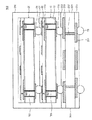
図14乃至図16は本発明の実施形態による半導体パッケージの断面図である。
100・・・基板
108・・・金属層
107・・・合金層
110・・・上部配線
114・・・下部保護膜
116・・・下部配線
118・・・バンプ
120・・・導電性連結部
124・・・上部保護膜
131・・・バリアー層
133・・・ライナー絶縁膜
171・・・ビアホール
BD・・・ボディー部
EX・・・延長部
TS・・・貫通電極
Claims (28)
- 第1面及び前記第1面に対向する第2面を含む基板と、
前記基板を貫通するビアホール内の貫通電極と、を含む半導体装置であって、
前記貫通電極は、
前記ビアホールの一部を満たす金属層と、
前記ビアホールの残りの部分を満たす合金層と、を含み、
前記合金層の結晶粒の大きさは、前記金属層の結晶粒の大きさより小さく、
前記合金層は、前記金属層に含まれた金属元素及び前記金属層に含まれた金属元素と異なる金属元素の少なくとも二つの金属元素を含み、
前記貫通電極は、前記金属層と前記合金層との間の分離導電層をさらに含み、
前記金属層と前記合金層とは、前記分離導電層によって分離されている半導体装置。 - 前記貫通電極は、前記第1面に隣接する上面及び前記第2面に隣接する下面を含み、
前記合金層は、前記貫通電極の上面の少なくとも一部を提供している請求項1に記載の半導体装置。 - 前記金属層は、前記合金層の側壁と前記ビアホールの側壁との間に介在した延長部を含む請求項1に記載の半導体装置。
- 前記合金層上面の直径は、前記延長部の水平方向の厚さより大きい請求項3に記載の半導体装置。
- 前記貫通電極と隣接して前記第1面上に提供された集積回路と、
前記貫通電極と前記集積回路とを電気的に連結する上部配線をさらに含み、
前記金属層と前記合金層とは、前記上部配線と共通的に接している請求項3に記載の半導体装置。 - 前記貫通電極は、前記ビアホールの側壁に沿って提供されるバリアー層をさらに含み、
前記合金層は、前記バリアー層と接している請求項1に記載の半導体装置。 - 前記合金層の厚さは、前記貫通電極の全体の垂直方向の長さの約2%乃至約15%である請求項1に記載の半導体装置。
- 前記金属層の平均結晶粒の大きさは、前記合金層の平均結晶粒の大きさの少なくとも2倍より大きい請求項1に記載の半導体装置。
- 前記合金層は、銅合金又はタングステン合金を含む請求項1に記載の半導体装置。
- 前記金属層は、銅(Cu)を含み、前記合金層は、Cu−Mn合金(Mnは5atm%乃至8atm%)、Cu−Au合金(Auは10atm%以上)、又はCu−Ni合金(Niは2atm%以上)の中の少なくとも1つを含む請求項1に記載の半導体装置。
- 前記金属層は、タングステン(W)を含み、前記合金層は、W−Mn合金(Mnは5atm%乃至8atm%)、W−Au合金(Auは10atm%以上)、又はW−Ni合金(Niは2atm%以上)の中の少なくとも1つを含む請求項1に記載の半導体装置。
- 前記貫通電極と隣接して前記第1面上に提供された集積回路と、
前記集積回路を覆う第1層間絶縁膜をさらに含み、
前記貫通電極は、前記第1層間絶縁膜の上面まで延長された請求項1に記載の半導体装置。 - 前記合金層は、前記第1面より高い下面を有している請求項12に記載の半導体装置。
- 前記貫通電極と隣接して前記第1面上に提供された集積回路と、
前記集積回路を覆う第1層間絶縁膜をさらに含み、
前記第1層間絶縁膜は、前記貫通電極の上面を覆っている請求項1に記載の半導体装置。 - 前記貫通電極と隣接して前記第1面上に提供された集積回路と、
前記集積回路を覆う第1層間絶縁膜と、
前記第1層間絶縁膜上の金属配線と、
前記金属配線上の第2層間絶縁膜と、をさらに含み、
前記貫通電極は、前記第2層間絶縁膜の上面まで延長された請求項1に記載の半導体装置。 - 活性面、前記活性面と対向する非活性面を含む基板であって、前記基板を貫通して前記活性面から前記非活性面まで延在しているビアホールをさらに含む基板と、
前記ビアホールの側壁に沿って提供されるバリアー層と、
前記ビアホール内の貫通電極と、を含み、
前記貫通電極は、前記ビアホールの一部を満たす金属層、及び前記金属層上に提供され、前記金属層に含まれた金属元素と異なる少なくとも一つの金属元素を含む合金層を含み、
前記金属層は、前記合金層の側壁と前記バリアー層との間に介在した延長部を含み、
前記貫通電極は、前記金属層と前記合金層との間の分離導電層をさらに含み、
前記金属層と前記合金層とは、前記分離導電層によって分離されている半導体装置。 - 前記金属層は、前記合金層下のボディー部をさらに含み、
前記延長部の結晶粒の大きさは、前記ボディー部の結晶粒大きさより小さい請求項16に記載の半導体装置。 - 前記貫通電極と隣接して前記基板の活性面上に提供された集積回路と、
前記貫通電極と前記集積回路とを電気的に連結する上部配線と、をさらに含み、
前記金属層と前記合金層とは、前記上部配線と共通的に接している請求項16に記載の半導体装置。 - 前記集積回路を覆う層間絶縁膜をさらに含み、
前記貫通電極は、前記層間絶縁膜を貫通して前記上部配線と連結される請求項18に記載の半導体装置。 - 前記合金層は、前記活性面より高い下面を有している請求項19に記載の半導体装置。
- 前記延長部は、前記ビアホールの前記側壁に対して斜めに傾いた内側壁を有している請求項16に記載の半導体装置。
- 前記合金層は、前記金属層に含まれた金属元素をさらに含む請求項16に記載の半導体装置。
- 半導体基板及び前記半導体基板上の層間絶縁膜を含む半導体チップを含み、
前記半導体チップは、前記半導体チップの少なくとも一部を貫通するように垂直延長する貫通電極を含み、
前記貫通電極は、金属層及び前記金属層に隣接する合金層を含み、
前記合金層は、少なくとも2つの金属元素を含み、前記少なくとも2つの金属元素は、前記金属層に含まれた金属元素及び前記金属層に含まれた金属元素と異なる金属元素を含み、
前記合金層の結晶粒の大きさは、前記金属層の結晶粒の大きさより小さく、
前記貫通電極は、前記金属層と前記合金層との間の分離導電層をさらに含み、
前記金属層と前記合金層とは、前記分離導電層によって分離されている半導体装置。 - 前記層間絶縁膜は、順に積層された第1層間絶縁膜及び第2層間絶縁膜を含み、前記貫通電極は、前記基板及び前記第1層間絶縁膜を貫通する請求項23に記載の半導体装置。
- 前記貫通電極は、前記第2層間絶縁膜を貫通しない請求項24に記載の半導体装置。
- 前記層間絶縁膜は、順に積層された第1層間絶縁膜及び第2層間絶縁膜を含み、前記貫通電極は、前記半導体基板を貫通する請求項23に記載の半導体装置。
- 前記貫通電極は、前記第1及び第2層間絶縁膜を貫通しない請求項26に記載の半導体装置。
- 前記層間絶縁膜は、順に積層された第1層間絶縁膜及び第2層間絶縁膜を含み、前記貫通電極は、前記基板、前記第1層間絶縁膜、及び前記第2層間絶縁膜を貫通する請求項23に記載の半導体装置。
Applications Claiming Priority (2)
| Application Number | Priority Date | Filing Date | Title |
|---|---|---|---|
| KR1020120106707A KR101992352B1 (ko) | 2012-09-25 | 2012-09-25 | 반도체 장치 |
| KR10-2012-0106707 | 2012-09-25 |
Publications (3)
| Publication Number | Publication Date |
|---|---|
| JP2014068014A JP2014068014A (ja) | 2014-04-17 |
| JP2014068014A5 JP2014068014A5 (ja) | 2015-11-12 |
| JP5865881B2 true JP5865881B2 (ja) | 2016-02-17 |
Family
ID=50338075
Family Applications (1)
| Application Number | Title | Priority Date | Filing Date |
|---|---|---|---|
| JP2013197964A Active JP5865881B2 (ja) | 2012-09-25 | 2013-09-25 | 半導体装置及びその製造方法 |
Country Status (3)
| Country | Link |
|---|---|
| US (2) | US9153522B2 (ja) |
| JP (1) | JP5865881B2 (ja) |
| KR (1) | KR101992352B1 (ja) |
Families Citing this family (21)
| Publication number | Priority date | Publication date | Assignee | Title |
|---|---|---|---|---|
| US9673132B2 (en) * | 2012-04-27 | 2017-06-06 | Taiwan Semiconductor Manufacting Company, Ltd. | Interconnection structure with confinement layer |
| KR20140011137A (ko) * | 2012-07-17 | 2014-01-28 | 삼성전자주식회사 | Tsv 구조를 구비한 집적회로 소자 및 그 제조 방법 |
| EP2893553A4 (en) * | 2012-09-05 | 2016-05-11 | Res Triangle Inst | ELECTRONIC DEVICES USING SPEED CONTACT PADS AND METHODS OF MAKING |
| US9514986B2 (en) * | 2013-08-28 | 2016-12-06 | Taiwan Semiconductor Manufacturing Company, Ltd. | Device with capped through-substrate via structure |
| US9865523B2 (en) | 2014-01-17 | 2018-01-09 | Taiwan Semiconductor Manufacturing Company, Ltd. | Robust through-silicon-via structure |
| US9583417B2 (en) * | 2014-03-12 | 2017-02-28 | Invensas Corporation | Via structure for signal equalization |
| KR102320821B1 (ko) | 2014-09-11 | 2021-11-02 | 삼성전자주식회사 | 반도체 패키지 |
| DE102014115105B4 (de) | 2014-10-09 | 2023-06-22 | Taiwan Semiconductor Manufacturing Company, Ltd. | Halbleitereinrichtung und Verfahren zur Herstellung einer Halbleitereinrichtung |
| JP2016139648A (ja) | 2015-01-26 | 2016-08-04 | 株式会社東芝 | 半導体装置及びその製造方法 |
| US10074594B2 (en) * | 2015-04-17 | 2018-09-11 | Taiwan Semiconductor Manufacturing Company Ltd. | Semiconductor structure and manufacturing method thereof |
| US9761509B2 (en) | 2015-12-29 | 2017-09-12 | United Microelectronics Corp. | Semiconductor device with throgh-substrate via and method for fabrication the semiconductor device |
| US10050139B2 (en) | 2016-06-24 | 2018-08-14 | Infineon Technologies Ag | Semiconductor device including a LDMOS transistor and method |
| US10242932B2 (en) | 2016-06-24 | 2019-03-26 | Infineon Technologies Ag | LDMOS transistor and method |
| US10622284B2 (en) | 2016-06-24 | 2020-04-14 | Infineon Technologies Ag | LDMOS transistor and method |
| US9875933B2 (en) | 2016-06-24 | 2018-01-23 | Infineon Technologies Ag | Substrate and method including forming a via comprising a conductive liner layer and conductive plug having different microstructures |
| US10432172B2 (en) | 2016-09-01 | 2019-10-01 | Samsung Electro-Mechanics Co., Ltd. | Bulk acoustic filter device and method of manufacturing the same |
| US10276528B2 (en) * | 2017-07-18 | 2019-04-30 | Taiwan Semiconductor Manufacturing Co., Ltd. | Semicondcutor device and manufacturing method thereof |
| KR102542614B1 (ko) * | 2017-10-30 | 2023-06-15 | 삼성전자주식회사 | 이미지 센서 |
| JP7219598B2 (ja) * | 2018-11-27 | 2023-02-08 | 新光電気工業株式会社 | 配線基板及びその製造方法 |
| US11398408B2 (en) * | 2019-09-24 | 2022-07-26 | Advanced Semiconductor Engineering, Inc. | Semiconductor substrate with trace connected to via at a level within a dielectric layer |
| KR20230024298A (ko) * | 2020-06-17 | 2023-02-20 | 도쿄엘렉트론가부시키가이샤 | 표면 세정 공정을 이용한 영역 선택적 증착 방법 |
Family Cites Families (36)
| Publication number | Priority date | Publication date | Assignee | Title |
|---|---|---|---|---|
| US5262354A (en) * | 1992-02-26 | 1993-11-16 | International Business Machines Corporation | Refractory metal capped low resistivity metal conductor lines and vias |
| US5300813A (en) * | 1992-02-26 | 1994-04-05 | International Business Machines Corporation | Refractory metal capped low resistivity metal conductor lines and vias |
| MY128333A (en) * | 1998-09-14 | 2007-01-31 | Ibiden Co Ltd | Printed wiring board and its manufacturing method |
| US6884335B2 (en) * | 2003-05-20 | 2005-04-26 | Novellus Systems, Inc. | Electroplating using DC current interruption and variable rotation rate |
| US7019402B2 (en) | 2003-10-17 | 2006-03-28 | International Business Machines Corporation | Silicon chip carrier with through-vias using laser assisted chemical vapor deposition of conductor |
| US6979625B1 (en) * | 2003-11-12 | 2005-12-27 | Advanced Micro Devices, Inc. | Copper interconnects with metal capping layer and selective copper alloys |
| US8084866B2 (en) | 2003-12-10 | 2011-12-27 | Micron Technology, Inc. | Microelectronic devices and methods for filling vias in microelectronic devices |
| JP4800585B2 (ja) | 2004-03-30 | 2011-10-26 | ルネサスエレクトロニクス株式会社 | 貫通電極の製造方法、シリコンスペーサーの製造方法 |
| US7232513B1 (en) * | 2004-06-29 | 2007-06-19 | Novellus Systems, Inc. | Electroplating bath containing wetting agent for defect reduction |
| US8004087B2 (en) * | 2004-08-12 | 2011-08-23 | Nec Corporation | Semiconductor device with dual damascene wirings and method for manufacturing same |
| US7946331B2 (en) * | 2005-06-14 | 2011-05-24 | Cufer Asset Ltd. L.L.C. | Pin-type chip tooling |
| JP4552770B2 (ja) | 2005-06-21 | 2010-09-29 | パナソニック電工株式会社 | 半導体基板への貫通配線の形成方法 |
| JP2007005404A (ja) | 2005-06-21 | 2007-01-11 | Matsushita Electric Works Ltd | 半導体基板への貫通配線の形成方法 |
| JP4581864B2 (ja) | 2005-06-21 | 2010-11-17 | パナソニック電工株式会社 | 半導体基板への貫通配線の形成方法 |
| US7528006B2 (en) | 2005-06-30 | 2009-05-05 | Intel Corporation | Integrated circuit die containing particle-filled through-silicon metal vias with reduced thermal expansion |
| US7772116B2 (en) * | 2005-09-01 | 2010-08-10 | Micron Technology, Inc. | Methods of forming blind wafer interconnects |
| US7892972B2 (en) * | 2006-02-03 | 2011-02-22 | Micron Technology, Inc. | Methods for fabricating and filling conductive vias and conductive vias so formed |
| JP5231733B2 (ja) | 2006-11-27 | 2013-07-10 | パナソニック株式会社 | 貫通孔配線構造およびその形成方法 |
| US7939941B2 (en) | 2007-06-27 | 2011-05-10 | Taiwan Semiconductor Manufacturing Company, Ltd. | Formation of through via before contact processing |
| US7973416B2 (en) * | 2008-05-12 | 2011-07-05 | Texas Instruments Incorporated | Thru silicon enabled die stacking scheme |
| US7678696B2 (en) | 2008-08-08 | 2010-03-16 | International Business Machines Corporation | Method of making through wafer vias |
| KR20100021856A (ko) | 2008-08-18 | 2010-02-26 | 삼성전자주식회사 | 관통 전극을 갖는 반도체장치의 형성방법 및 관련된 장치 |
| US8097953B2 (en) | 2008-10-28 | 2012-01-17 | Taiwan Semiconductor Manufacturing Company, Ltd. | Three-dimensional integrated circuit stacking-joint interface structure |
| US20100200408A1 (en) * | 2009-02-11 | 2010-08-12 | United Solar Ovonic Llc | Method and apparatus for the solution deposition of high quality oxide material |
| US8610283B2 (en) * | 2009-10-05 | 2013-12-17 | International Business Machines Corporation | Semiconductor device having a copper plug |
| KR101302564B1 (ko) | 2009-10-28 | 2013-09-02 | 한국전자통신연구원 | 비아 형성 방법 및 이를 이용하는 적층 칩 패키지의 제조 방법 |
| KR20110050957A (ko) * | 2009-11-09 | 2011-05-17 | 삼성전자주식회사 | 반도체 소자의 관통 비아 콘택 및 그 형성 방법 |
| US8304863B2 (en) * | 2010-02-09 | 2012-11-06 | International Business Machines Corporation | Electromigration immune through-substrate vias |
| JP2011216867A (ja) * | 2010-03-17 | 2011-10-27 | Tokyo Electron Ltd | 薄膜の形成方法 |
| KR101692434B1 (ko) | 2010-06-28 | 2017-01-18 | 삼성전자주식회사 | 반도체 소자 및 그 제조 방법 |
| JP5504147B2 (ja) * | 2010-12-21 | 2014-05-28 | 株式会社荏原製作所 | 電気めっき方法 |
| JP2012151435A (ja) | 2010-12-27 | 2012-08-09 | Elpida Memory Inc | 半導体装置の製造方法 |
| KR101541056B1 (ko) * | 2011-09-13 | 2015-07-31 | 아데스토 테크놀러지스 코포레이션 | 합금 전극을 갖는 저항 스위칭 디바이스 및 그 형성 방법 |
| US8785790B2 (en) * | 2011-11-10 | 2014-07-22 | Invensas Corporation | High strength through-substrate vias |
| US9269612B2 (en) * | 2011-11-22 | 2016-02-23 | Taiwan Semiconductor Manufacturing Company, Ltd. | Mechanisms of forming damascene interconnect structures |
| KR20140011137A (ko) * | 2012-07-17 | 2014-01-28 | 삼성전자주식회사 | Tsv 구조를 구비한 집적회로 소자 및 그 제조 방법 |
-
2012
- 2012-09-25 KR KR1020120106707A patent/KR101992352B1/ko active IP Right Grant
-
2013
- 2013-09-16 US US14/028,523 patent/US9153522B2/en active Active
- 2013-09-25 JP JP2013197964A patent/JP5865881B2/ja active Active
-
2015
- 2015-07-24 US US14/809,159 patent/US9679829B2/en active Active
Also Published As
| Publication number | Publication date |
|---|---|
| US20150332967A1 (en) | 2015-11-19 |
| KR101992352B1 (ko) | 2019-06-24 |
| JP2014068014A (ja) | 2014-04-17 |
| US20140084473A1 (en) | 2014-03-27 |
| KR20140039895A (ko) | 2014-04-02 |
| US9679829B2 (en) | 2017-06-13 |
| US9153522B2 (en) | 2015-10-06 |
Similar Documents
| Publication | Publication Date | Title |
|---|---|---|
| JP5865881B2 (ja) | 半導体装置及びその製造方法 | |
| US9824973B2 (en) | Integrated circuit devices having through-silicon via structures and methods of manufacturing the same | |
| KR102064863B1 (ko) | 관통 비아 구조체를 갖는 반도체 소자 제조 방법 | |
| US9543250B2 (en) | Semiconductor devices including through-silicon via | |
| KR101931115B1 (ko) | 반도체 장치 및 그 제조 방법 | |
| US9153559B2 (en) | Semiconductor devices including through silicon via electrodes and methods of fabricating the same | |
| US8586477B2 (en) | Semiconductor apparatus, method of manufacturing the same, and method of manufacturing semiconductor package | |
| US20150130078A1 (en) | Semiconductor chip and semiconductor package having same | |
| US20150123278A1 (en) | Semiconductor devices, methods of manufacturing the same, memory cards including the same and electronic systems including the same | |
| KR20100021856A (ko) | 관통 전극을 갖는 반도체장치의 형성방법 및 관련된 장치 | |
| JP2012044168A (ja) | 積層半導体装置及び積層半導体装置の製造方法 | |
| US20140141569A1 (en) | Semiconductor devices having through-via and methods of fabricating the same | |
| US20140138819A1 (en) | Semiconductor device including tsv and semiconductor package including the same | |
| JP2013070057A (ja) | 半導体チップ、これを含む半導体パッケージ、及びその製造方法 | |
| KR20140104778A (ko) | 관통전극을 갖는 반도체 소자의 제조방법 | |
| KR101095373B1 (ko) | 장벽층을 갖는 범프를 포함하는 반도체칩 및 그 제조방법 | |
| KR20120091867A (ko) | CoC 구조의 반도체 패키지 및 그 패키지 제조방법 | |
| US9431332B2 (en) | Semiconductor package | |
| US8754531B2 (en) | Through-silicon via with a non-continuous dielectric layer | |
| US9059067B2 (en) | Semiconductor device with interposer and method manufacturing same | |
| KR20150019089A (ko) | 관통전극을 갖는 반도체 소자 및 그 제조방법 | |
| US20120049349A1 (en) | Semiconductor chips and methods of forming the same | |
| TW201501256A (zh) | 中介板及其製法 | |
| US9281274B1 (en) | Integrated circuit through-substrate via system with a buffer layer and method of manufacture thereof | |
| WO2022088092A1 (zh) | 膜层穿孔的形成方法、半导体器件及芯片 |
Legal Events
| Date | Code | Title | Description |
|---|---|---|---|
| RD04 | Notification of resignation of power of attorney |
Free format text: JAPANESE INTERMEDIATE CODE: A7424 Effective date: 20141226 |
|
| A521 | Request for written amendment filed |
Free format text: JAPANESE INTERMEDIATE CODE: A523 Effective date: 20150924 |
|
| A621 | Written request for application examination |
Free format text: JAPANESE INTERMEDIATE CODE: A621 Effective date: 20150924 |
|
| A871 | Explanation of circumstances concerning accelerated examination |
Free format text: JAPANESE INTERMEDIATE CODE: A871 Effective date: 20150924 |
|
| A975 | Report on accelerated examination |
Free format text: JAPANESE INTERMEDIATE CODE: A971005 Effective date: 20151124 |
|
| TRDD | Decision of grant or rejection written | ||
| A01 | Written decision to grant a patent or to grant a registration (utility model) |
Free format text: JAPANESE INTERMEDIATE CODE: A01 Effective date: 20151130 |
|
| A61 | First payment of annual fees (during grant procedure) |
Free format text: JAPANESE INTERMEDIATE CODE: A61 Effective date: 20151228 |
|
| R150 | Certificate of patent or registration of utility model |
Ref document number: 5865881 Country of ref document: JP Free format text: JAPANESE INTERMEDIATE CODE: R150 |
|
| R250 | Receipt of annual fees |
Free format text: JAPANESE INTERMEDIATE CODE: R250 |
|
| R250 | Receipt of annual fees |
Free format text: JAPANESE INTERMEDIATE CODE: R250 |
|
| R250 | Receipt of annual fees |
Free format text: JAPANESE INTERMEDIATE CODE: R250 |
|
| R250 | Receipt of annual fees |
Free format text: JAPANESE INTERMEDIATE CODE: R250 |
|
| R250 | Receipt of annual fees |
Free format text: JAPANESE INTERMEDIATE CODE: R250 |
|
| R250 | Receipt of annual fees |
Free format text: JAPANESE INTERMEDIATE CODE: R250 |