JP5840887B2 - Thermal head and thermal printer equipped with the same - Google Patents

Thermal head and thermal printer equipped with the same Download PDF

Info

Publication number
JP5840887B2
JP5840887B2 JP2011167164A JP2011167164A JP5840887B2 JP 5840887 B2 JP5840887 B2 JP 5840887B2 JP 2011167164 A JP2011167164 A JP 2011167164A JP 2011167164 A JP2011167164 A JP 2011167164A JP 5840887 B2 JP5840887 B2 JP 5840887B2
Authority
JP
Japan
Prior art keywords
heat generating
conductive
thermal head
electrode
portions
Prior art date
Legal status (The legal status is an assumption and is not a legal conclusion. Google has not performed a legal analysis and makes no representation as to the accuracy of the status listed.)
Active
Application number
JP2011167164A
Other languages
Japanese (ja)
Other versions
JP2013028136A (en
Inventor
新谷 重孝
重孝 新谷
Current Assignee (The listed assignees may be inaccurate. Google has not performed a legal analysis and makes no representation or warranty as to the accuracy of the list.)
Kyocera Corp
Original Assignee
Kyocera Corp
Priority date (The priority date is an assumption and is not a legal conclusion. Google has not performed a legal analysis and makes no representation as to the accuracy of the date listed.)
Filing date
Publication date
Application filed by Kyocera Corp filed Critical Kyocera Corp
Priority to JP2011167164A priority Critical patent/JP5840887B2/en
Publication of JP2013028136A publication Critical patent/JP2013028136A/en
Application granted granted Critical
Publication of JP5840887B2 publication Critical patent/JP5840887B2/en
Active legal-status Critical Current
Anticipated expiration legal-status Critical

Links

Images

Description

本発明は、サーマルヘッドおよびこれを備えるサーマルプリンタに関する。   The present invention relates to a thermal head and a thermal printer including the same.

従来、ファクシミリ、ビデオプリンタあるいはカードプリンタ等の印画デバイスとして、種々のサーマルヘッドが提案されている。これらのサーマルヘッドとしては、発熱部に生じる温度分布を均一に近づけるために、発熱部の幅方向における中央部が突出したサーマルヘッドが知られている(特許文献1参照)。   Conventionally, various thermal heads have been proposed as printing devices such as facsimiles, video printers and card printers. As these thermal heads, there is known a thermal head in which a central portion in the width direction of the heat generating portion protrudes in order to make the temperature distribution generated in the heat generating portion close to uniform (see Patent Document 1).

特開昭61−152467号公報JP 61-152467 A

しかしながら、上記のサーマルヘッドにおいては、発熱部に生じる温度分布をある程度均一に近づけることができるものの、発熱部の幅方向における中央部が突出しているため、画素が発熱部の形状と相似した形状となり、画素間に隙間が生じてしまい、画素再現性が低いという問題がある。   However, in the above thermal head, the temperature distribution generated in the heat generating part can be made somewhat uniform, but since the central part in the width direction of the heat generating part protrudes, the pixel has a shape similar to the shape of the heat generating part. There is a problem that gaps are generated between the pixels and the pixel reproducibility is low.

本発明のサーマルヘッドは、複数の発熱部と、発熱部と接続された一対の電極とを備えるものにおいて、発熱部が矩形状である。また、電極は、第1導電部と、発熱部と第1導電部とを接続する第2導電部とを有しており、第1導電部は、第1導電部の幅方向における中央部に、発熱部側に突出した突出部が設けられている。また、突出部は、発熱部と離間して配置されている。 The thermal head of the present invention includes a plurality of heat generating portions and a pair of electrodes connected to the heat generating portions, and the heat generating portions are rectangular. The electrode also includes a first conductive portion and a second conductive portion that connects the heat generating portion and the first conductive portion. The first conductive portion is located at a central portion in the width direction of the first conductive portion. A protruding portion that protrudes toward the heat generating portion is provided. Further, the protruding portion is disposed away from the heat generating portion.

また、本発明のサーマルプリンタは、上記のいずれかに記載のサーマルヘッドと、発熱部上に記録媒体を搬送する搬送機構と、発熱部上に記録媒体を押圧するプラテンローラとを備える。   The thermal printer of the present invention includes any one of the thermal heads described above, a transport mechanism that transports the recording medium onto the heat generating portion, and a platen roller that presses the recording medium onto the heat generating portion.

本発明によれば、発熱部に生じる温度分布を均一に近づけることができ、サーマルヘッドの画素再現性を高めることができる。   According to the present invention, the temperature distribution generated in the heat generating portion can be made to be uniform, and the pixel reproducibility of the thermal head can be improved.

本発明の一実施形態に係るサーマルヘッドの平面図である。It is a top view of the thermal head concerning one embodiment of the present invention. 図1のサーマルヘッドのI−I線断面図である。It is the II sectional view taken on the line of the thermal head of FIG. 図1のサーマルヘッドのII−II線断面図である。It is the II-II sectional view taken on the line of the thermal head of FIG. 図1の外部基板を省略した平面図である。It is the top view which abbreviate | omitted the external board | substrate of FIG. 図1のサーマルヘッドの発熱部と電極との関係を示し、(a)は概略斜視図、(b)は概略平面図である。The relationship between the heat generating part and electrode of the thermal head of FIG. 1 is shown, (a) is a schematic perspective view, (b) is a schematic plan view. (a)は図5(b)に示すIII−III線断面図であり、(b)は発熱部の温度分布を示す概念図である。(A) is the III-III sectional view taken on the line shown in FIG.5 (b), (b) is a conceptual diagram which shows the temperature distribution of a heat-emitting part. 本発明の一実施形態に係るサーマルプリンタを示す概略構成図である。1 is a schematic configuration diagram illustrating a thermal printer according to an embodiment of the present invention. 本発明の他の実施形態に係るサーマルヘッドにおける発熱部と電極との関係を示す概略斜視図である。It is a schematic perspective view which shows the relationship between the heat generating part and electrode in the thermal head which concerns on other embodiment of this invention. (a)は図8に示すサーマルヘッドの平面図、(b)は(a)に示すIV-IV線断面図、(c)は(a)に示すV-V線断面図である。(A) is a plan view of the thermal head shown in FIG. 8, (b) is a sectional view taken along line IV-IV shown in (a), and (c) is a sectional view taken along line VV shown in (a). 本発明のさらに他の実施形態に係るサーマルヘッドにおける発熱部と電極との関係を示し、(a)は概略斜視図、(b)は概略平面図、(c)は発熱部の温度分布を示す概念平面図である。The relationship between the heat generating part and the electrode in the thermal head which concerns on further another embodiment of this invention is shown, (a) is a schematic perspective view, (b) is a schematic plan view, (c) shows the temperature distribution of a heat generating part. It is a conceptual top view. 本発明のさらに他の実施形態に係るサーマルヘッドにおける発熱部と電極との関係を示し、(a)は概略斜視図、(b)は概略平面図である。The relationship between the heat generating part and the electrode in the thermal head which concerns on further another embodiment of this invention is shown, (a) is a schematic perspective view, (b) is a schematic plan view.

<第1の実施形態>
以下、本発明のサーマルヘッドの一実施形態について、図面を参照しつつ説明する。なお、図1〜6、8〜11に記載したD1とはサーマルヘッドの幅方向、D2とはサーマルヘッドの長手方向、D3とはサーマルヘッドの厚み方向を示し、以下、それぞれD1方向、D2方向、およびD3方向と称する場合がある。
<First Embodiment>
Hereinafter, an embodiment of a thermal head of the present invention will be described with reference to the drawings. 1 to 6 and 8 to 11, D1 is the width direction of the thermal head, D2 is the longitudinal direction of the thermal head, D3 is the thickness direction of the thermal head, and hereinafter, D1 direction and D2 direction, respectively. , And D3 direction.

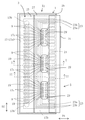
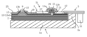
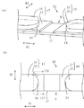
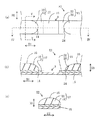
図1〜4に示すように、本実施形態のサーマルヘッドX1は、放熱体1と、放熱体1上に配置されたヘッド基体3と、ヘッド基体3に接続された外部基板であるフレキシブルプリント配線板5(以下、FPC5という)とを備えている。   As shown in FIGS. 1 to 4, the thermal head X <b> 1 of the present embodiment includes a radiator 1, a head substrate 3 disposed on the radiator 1, and a flexible printed wiring that is an external substrate connected to the head substrate 3. A plate 5 (hereinafter referred to as FPC 5) is provided.

放熱体1は、例えば、CuまたはAl等の金属材料で形成されており、平面視して矩形状である台板部1aと、この台板部1aの一方の長辺に沿って延びる突出部1bとを備えている。図2、3に示すように、突出部1bを除いた台板部1aの上面には、図示していないが、両面テープや接着剤等によってヘッド基体3が接着されている。同様に、突出部1b上には、両面テープや接着剤等によってFPC5が接着されている。また、放熱体1は、後述するようにヘッド基体3の発熱部9で発生した熱のうち、印画に寄与しない熱の一部を放熱する機能を有している。   The radiator 1 is made of, for example, a metal material such as Cu or Al, and has a base plate portion 1a that is rectangular in plan view, and a protruding portion that extends along one long side of the base plate portion 1a. 1b. As shown in FIGS. 2 and 3, the head substrate 3 is bonded to the upper surface of the base plate 1a excluding the protruding portion 1b by a double-sided tape, an adhesive or the like, although not shown. Similarly, the FPC 5 is bonded onto the protruding portion 1b by a double-sided tape, an adhesive, or the like. The radiator 1 has a function of radiating a part of heat generated in the heat generating portion 9 of the head base 3 that does not contribute to printing, as will be described later.

図1〜4に示すように、ヘッド基体3は、平面視して矩形状の基板7と、基板7上に設けられ、基板7の長手方向に沿って列状に配列された複数の発熱部9と、発熱部9の配列方向に沿って基板7上に並べて配置された複数の駆動IC11とを備えている。   As shown in FIGS. 1 to 4, the head base 3 includes a rectangular substrate 7 in plan view and a plurality of heat generating portions provided on the substrate 7 and arranged in a line along the longitudinal direction of the substrate 7. 9 and a plurality of drive ICs 11 arranged side by side on the substrate 7 along the arrangement direction of the heat generating portions 9.

基板7は、アルミナセラミックス等の電気絶縁性材料や単結晶シリコン等の半導体材料等によって形成されている。   The substrate 7 is made of an electrically insulating material such as alumina ceramic, a semiconductor material such as single crystal silicon, or the like.

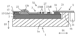
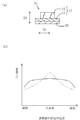
図2、3に示すように、基板7の上面には、蓄熱層13が形成されている。この蓄熱層13は、基板7の上面全体に形成された下地部13aと、この下地部13aから部分的に隆起するとともに複数の発熱部9の配列方向に沿って帯状に延び、断面が略半楕円形状の隆起部13bとを有している。この隆起部13bは、印画する記録媒体を、発熱部9上に形成された後述する保護膜25に良好に押し当てるように機能する。   As shown in FIGS. 2 and 3, a heat storage layer 13 is formed on the upper surface of the substrate 7. The heat storage layer 13 has a base portion 13a formed on the entire upper surface of the substrate 7, and partially protrudes from the base portion 13a and extends in a strip shape along the direction in which the plurality of heat generating portions 9 are arranged. And an elliptical raised portion 13b. The raised portion 13b functions to favorably press the recording medium to be printed against a protective film 25 described later formed on the heat generating portion 9.

蓄熱層13は、例えば、熱伝導性の低いガラスで形成されており、発熱部9で発生する熱の一部を一時的に蓄積することで、発熱部9の温度を上昇させるのに要する時間を短くし、サーマルヘッドX1の熱応答特性を高めるように作用する。この蓄熱層13は、例えば、ガラス粉末に適当な有機溶剤を混合して得た所定のガラスペーストを従来周知のスクリーン印刷等によって基板7の上面に塗布し、これを高温で焼成することで形成される。蓄熱層13を形成するガラスとしては、例えば、SiO、Al、CaOおよびBaOを含有するもの、SiO、AlおよびPbOを含有するもの、SiO、AlおよびBaOを含有するもの、SiO、B、PbO、Al、CaOおよびMgOを含有するものが挙げられる。 The heat storage layer 13 is formed of, for example, glass having low thermal conductivity, and the time required to raise the temperature of the heat generating part 9 by temporarily storing a part of the heat generated in the heat generating part 9. And the thermal response characteristic of the thermal head X1 is enhanced. The heat storage layer 13 is formed, for example, by applying a predetermined glass paste obtained by mixing a glass powder with an appropriate organic solvent onto the upper surface of the substrate 7 by screen printing or the like, and baking it at a high temperature. Is done. Examples of the glass forming the heat storage layer 13 include those containing SiO 2 , Al 2 O 3 , CaO and BaO, those containing SiO 2 , Al 2 O 3 and PbO, SiO 2 , Al 2 O 3 and Examples include those containing BaO, and those containing SiO 2 , B 2 O 3 , PbO, Al 2 O 3 , CaO and MgO.

蓄熱層13の上面には、電気抵抗層15が設けられている。この電気抵抗層15は、蓄
熱層13と、後述する共通電極17、個別電極19、グランド電極21およびIC制御配線23との間に介在し、図4に示すように、平面視して、これらの個別電極19、共通電極17、グランド電極21およびIC制御配線23と同形状の領域(以下、介在領域という)と、個別電極19と共通電極17との間から露出した複数の領域(以下、露出領域という)とを有している。
An electrical resistance layer 15 is provided on the upper surface of the heat storage layer 13. The electric resistance layer 15 is interposed between the heat storage layer 13 and a common electrode 17, an individual electrode 19, a ground electrode 21, and an IC control wiring 23 which will be described later. Of the individual electrode 19, the common electrode 17, the ground electrode 21, and the IC control wiring 23 (hereinafter referred to as an intervening region), and a plurality of regions exposed from between the individual electrode 19 and the common electrode 17 (hereinafter referred to as intervening regions). The exposure area).

電気抵抗層15は、蓄熱層13の隆起部13b上に列状に配列されている。複数の発熱部9は、説明の便宜上、図1〜4では簡略化して記載しているが、例えば、180〜2400dpi程度の密度で配置される。   The electric resistance layer 15 is arranged in a row on the raised portion 13 b of the heat storage layer 13. The plurality of heat generating portions 9 are illustrated in a simplified manner in FIGS. 1 to 4 for convenience of explanation, but are arranged with a density of about 180 to 2400 dpi, for example.

電気抵抗層15は、例えば、TaN系、TaSiO系、TaSiNO系、TiSiO系、TiSiCO系またはNbSiO系等の電気抵抗の比較的高い材料によって形成されている。そのため、後述する共通電極17と個別電極19との間に電圧が印加され、発熱部9に電流が供給されたときに、ジュール発熱によって発熱部9が発熱する。なお、電気抵抗層15がこのような電気抵抗の比較的高い材料で形成されていることから、発熱部9が電気抵抗層15で形成されることとなる。   The electric resistance layer 15 is made of a material having a relatively high electric resistance, such as TaN, TaSiO, TaSiNO, TiSiO, TiSiCO, or NbSiO. Therefore, when a voltage is applied between the common electrode 17 and the individual electrode 19 which will be described later and a current is supplied to the heat generating portion 9, the heat generating portion 9 generates heat due to Joule heat generation. Since the electrical resistance layer 15 is formed of such a material having a relatively high electrical resistance, the heat generating portion 9 is formed of the electrical resistance layer 15.

図1〜4に示すように、電気抵抗層15の上面、より詳細には、上記の介在領域の上面には、共通電極17、個別電極19、グランド電極21およびIC制御配線23が設けられている。これらの共通電極17、個別電極19、グランド電極21およびIC制御配線23は、導電性を有する材料で形成されており、例えば、アルミニウム、金、銀および銅のうちのいずれか一種の金属またはこれらの合金によって形成されている。なお、図4は、後述する保護膜25、被覆層27および被覆部材29の図示を省略したヘッド基体3示す平面図である。   As shown in FIGS. 1 to 4, the common electrode 17, the individual electrode 19, the ground electrode 21, and the IC control wiring 23 are provided on the upper surface of the electric resistance layer 15, more specifically, on the upper surface of the intervening region. Yes. The common electrode 17, the individual electrode 19, the ground electrode 21, and the IC control wiring 23 are formed of a conductive material. For example, any one metal of aluminum, gold, silver, and copper, or these It is made of an alloy. FIG. 4 is a plan view showing the head base 3 in which a protective film 25, a covering layer 27, and a covering member 29 described later are not shown.

共通電極17は、図4に示すように、基板7の一方の長辺に沿って延びる主配線部17aと、基板7の一方および他方の短辺のそれぞれに沿って延び、一端部が主配線部17aに接続された2つの副配線部17bと、主配線部17aから各発熱部9に向かって延びる複数のリード部17cとを有している。また、リード部17cは、詳細は後述するが第1導電部10(図5参照)および第2導電部12(図5参照)を有している。そして、図4に示すように、副配線部17bの他端部がFPC5に接続されているとともに、第1導電部10と発熱部9とが第2導電部12により接続されている。これにより、FPC5と発熱部9との間が電気的に接続されている。   As shown in FIG. 4, the common electrode 17 extends along each of the main wiring portion 17 a extending along one long side of the substrate 7 and one and the other short sides of the substrate 7, and one end thereof is connected to the main wiring. Two sub-wiring portions 17b connected to the portion 17a and a plurality of lead portions 17c extending from the main wiring portion 17a toward the heat generating portions 9 are provided. The lead portion 17c has a first conductive portion 10 (see FIG. 5) and a second conductive portion 12 (see FIG. 5), details of which will be described later. As shown in FIG. 4, the other end portion of the sub wiring portion 17 b is connected to the FPC 5, and the first conductive portion 10 and the heat generating portion 9 are connected by the second conductive portion 12. Thereby, the FPC 5 and the heat generating part 9 are electrically connected.

個別電極19は、図1〜4に示すように、各発熱部9と駆動IC11との間に延びており、これらの間を接続している。より詳細には、個別電極19は、複数の発熱部9をそれぞれ複数の群に分け、各群の発熱部9を、各群に対応して設けられた駆動IC11に電気的に接続している。なお、個別電極19は、詳細は後述するが第1導電部20と第2導電部22とを有している。   As shown in FIGS. 1 to 4, the individual electrode 19 extends between each heat generating portion 9 and the drive IC 11, and connects between them. More specifically, the individual electrode 19 divides a plurality of heat generating portions 9 into a plurality of groups, and electrically connects the heat generating portions 9 of each group to a drive IC 11 provided corresponding to each group. . The individual electrode 19 has a first conductive portion 20 and a second conductive portion 22, which will be described in detail later.

グランド電極21は、図4に示すように、発熱部9の配列方向に直交する方向に沿って、基板7の他方の長辺の近傍で帯状に延びている。このグランド電極21上には、図3に示すように、FPC5および駆動IC11が接続されている。   As shown in FIG. 4, the ground electrode 21 extends in a band shape in the vicinity of the other long side of the substrate 7 along a direction orthogonal to the arrangement direction of the heat generating portions 9. On the ground electrode 21, as shown in FIG. 3, the FPC 5 and the drive IC 11 are connected.

駆動IC11は、図2に示すように、複数の発熱部9の各群に対応して配置されており、個別電極19の一端部とグランド電極21とに接続されている。この駆動IC11は、各発熱部9の通電状態を制御するためのものであり、後述するように、内部に複数のスイッチング素子(不図示)を有しており、スイッチング素子がオフ状態のときに不通電状態となる公知のものを用いることができる。各駆動IC11は、内部のスイッチング素子に接続されている一方の接続端子11a(以下、第1接続端子11aという)が個別電極1
9に接続されており、このスイッチング素子に接続されている他方の接続端子11b(以下、第2接続端子11bという)がグランド電極21に接続されている。これにより、駆動IC11の各スイッチング素子がオン状態のときに、各スイッチング素子に接続された個別電極19とグランド電極21とが電気的に接続される。
As shown in FIG. 2, the drive IC 11 is disposed corresponding to each group of the plurality of heat generating units 9, and is connected to one end of the individual electrode 19 and the ground electrode 21. This drive IC 11 is for controlling the energization state of each heat generating part 9, and has a plurality of switching elements (not shown) inside, as will be described later, and when the switching elements are in the OFF state. A well-known thing which will be in a non-energized state can be used. Each drive IC 11 has one connection terminal 11a (hereinafter referred to as a first connection terminal 11a) connected to an internal switching element as an individual electrode 1.
9, and the other connection terminal 11 b (hereinafter referred to as the second connection terminal 11 b) connected to the switching element is connected to the ground electrode 21. Thereby, when each switching element of the drive IC 11 is in the ON state, the individual electrode 19 connected to each switching element and the ground electrode 21 are electrically connected.

なお、図示していないが、個別電極19に接続された第1接続端子11aおよびグランド電極21に接続された第2接続端子11bは、各個別電極19に対応して複数個設けられている。この複数の第1接続端子11aは、各個別電極19に個別に接続されている。また、複数の第2接続端子11bは、グランド電極21に個別に接続されている。   Although not shown, a plurality of first connection terminals 11 a connected to the individual electrodes 19 and second connection terminals 11 b connected to the ground electrodes 21 are provided corresponding to the individual electrodes 19. The plurality of first connection terminals 11 a are individually connected to the individual electrodes 19. The plurality of second connection terminals 11 b are individually connected to the ground electrode 21.

IC制御配線23は、駆動IC11を制御するためのものであり、図1、4に示すように、IC電源配線23aとIC信号配線23bとを備えている。IC電源配線23aは、基板7の長手方向の両端部で基板7の右側の長辺の近傍に配置された端部電源配線部23aEと、隣接する駆動IC11間に配置された中間電源配線部23aMとを有している。   The IC control wiring 23 is for controlling the driving IC 11 and includes an IC power supply wiring 23a and an IC signal wiring 23b as shown in FIGS. The IC power supply wiring 23a is provided at both ends in the longitudinal direction of the substrate 7 at the end power supply wiring portion 23aE disposed near the right long side of the substrate 7 and the intermediate power supply wiring portion 23aM disposed between the adjacent drive ICs 11. And have.

図4に示すように、端部電源配線部23aEは、一端部が駆動IC11の配置領域に配置され、グランド電極21の周囲を回り込むようにして、他端部が基板7の右側の長辺の近傍に配置されている。この端部電源配線部23aEは、一端部が駆動IC11に接続されているとともに、他端部がFPC5に接続されている。これにより、駆動IC11とFPC5との間が電気的に接続されている。   As shown in FIG. 4, the end power supply wiring portion 23 a </ i> E has one end portion disposed in the region where the drive IC 11 is disposed and wraps around the ground electrode 21, and the other end portion is a long side on the right side of the substrate 7. It is arranged in the vicinity. The end power wiring portion 23aE has one end connected to the drive IC 11 and the other end connected to the FPC 5. Thereby, the drive IC 11 and the FPC 5 are electrically connected.

端部電源配線部23aEと中間電源配線部23aMとは、これらの双方が接続された駆動IC11の内部で電気的に接続されている。また、隣接する中間電源配線部23aM同士は、これらの双方が接続された駆動IC11の内部で電気的に接続されている。   The end power supply wiring portion 23aE and the intermediate power supply wiring portion 23aM are electrically connected inside the drive IC 11 to which both of them are connected. The adjacent intermediate power supply wiring portions 23aM are electrically connected inside the drive IC 11 to which both of them are connected.

このように、IC電源配線23aを各駆動IC11と接続することにより、IC電源配線23aが各駆動IC11とFPC5との間を電気的に接続している。これにより、後述するようにFPC5から端部電源配線部23aEおよび中間電源配線部23aMを介して各駆動IC11に電流を供給するようになっている。   Thus, by connecting the IC power supply wiring 23a to each drive IC 11, the IC power supply wiring 23a electrically connects each drive IC 11 and the FPC 5. Thereby, as will be described later, a current is supplied from the FPC 5 to each drive IC 11 via the end power supply wiring portion 23aE and the intermediate power supply wiring portion 23aM.

IC信号配線23bも同様に、図4に示すように、基板7の長手方向の両端部で基板7の右側の長辺の近傍に配置された端部信号配線部23bEと、隣接する駆動IC11間に配置された中間信号配線部23bMとを有している。   Similarly, as shown in FIG. 4, the IC signal wiring 23 b is also connected between the end signal wiring portion 23 b E arranged in the vicinity of the long side on the right side of the substrate 7 at both ends in the longitudinal direction of the substrate 7 and the adjacent driving IC 11. And an intermediate signal wiring portion 23bM.

なお、駆動IC11に接続される電極は、端部電源配線部23aE、23bE、中間信号配線部23aM、23bMを設けずに、個別電極19およびグランド電極21に接続されていてもよく、ヘッド基体3に駆動IC11を実装しなくともよい。   The electrodes connected to the drive IC 11 may be connected to the individual electrode 19 and the ground electrode 21 without providing the end power supply wiring portions 23aE and 23bE and the intermediate signal wiring portions 23aM and 23bM. It is not necessary to mount the driving IC 11 on the board.

上記の電気抵抗層15、共通電極17、個別電極19、グランド電極21およびIC制御配線23は、例えば、各々を構成する材料層を蓄熱層13上に、例えばスパッタリング法などの従来周知の薄膜成形技術によって順次積層した後、この積層体を従来周知のフォトリソグラフィー技術やエッチング技術等を用いて所定のパターンに加工することにより形成される。また、駆動IC11あるいは後述するFPC5と接合される共通電極17、個別電極19、グランド電極21およびIC制御配線23に、めっき法によりNiめっきを施すことにより、図示しないが電極パッドを形成して、電極パッドを介して共通電極17、個別電極19、グランド電極21およびIC制御配線23と駆動IC11あるいはFPC5とを接合する。なお、第1導電部10(図5参照)および第2導電部12(図5参照)の作製方法については後述する。   The electric resistance layer 15, common electrode 17, individual electrode 19, ground electrode 21, and IC control wiring 23 are, for example, a conventionally well-known thin film molding such as a sputtering method, for example, by forming a material layer constituting each of them on the heat storage layer 13. After sequentially laminating by a technique, this laminate is formed by processing it into a predetermined pattern using a conventionally known photolithography technique, etching technique or the like. Further, by performing Ni plating by plating on the common electrode 17, the individual electrode 19, the ground electrode 21 and the IC control wiring 23 to be joined to the driving IC 11 or the FPC 5 described later, an electrode pad (not shown) is formed, The common electrode 17, the individual electrode 19, the ground electrode 21, and the IC control wiring 23 are joined to the driving IC 11 or the FPC 5 through the electrode pad. A method for manufacturing the first conductive portion 10 (see FIG. 5) and the second conductive portion 12 (see FIG. 5) will be described later.

図1〜3に示すように、基板7の上面に形成された蓄熱層13上には、発熱部9、共通
電極17の一部および個別電極19の一部を被覆する保護膜25が形成されている。図示例では、この保護膜25は、複数の発熱部9の配列方向に沿って形成され、蓄熱層13の上面の略左半分の領域を覆うように設けられている。なお、図示していないが、保護膜25は、蓄熱層13上に形成された電気絶縁層と、電気絶縁層上に形成された封止層と、封止層上に形成された耐摩耗層とを有している。
As shown in FIGS. 1 to 3, a protective film 25 is formed on the heat storage layer 13 formed on the upper surface of the substrate 7 to cover the heat generating portion 9, a part of the common electrode 17 and a part of the individual electrode 19. ing. In the illustrated example, the protective film 25 is formed along the arrangement direction of the plurality of heat generating portions 9, and is provided so as to cover a substantially left half region of the upper surface of the heat storage layer 13. Although not shown, the protective film 25 includes an electrical insulating layer formed on the heat storage layer 13, a sealing layer formed on the electrical insulating layer, and a wear-resistant layer formed on the sealing layer. And have.

保護膜25を形成することにより、被覆した発熱部9、共通電極17および個別電極19の部分が、酸素との反応によって酸化することを抑制したり、大気中に含まれている水分等の付着によって腐食することを抑制したりすることもできる。この保護膜25を構成する電気絶縁層、封止層および耐摩耗層は、例えば、スパッタリング法、蒸着法等の従来周知の薄膜成形技術や、スクリーン印刷法等の厚膜成形技術を用いて形成することができる。   By forming the protective film 25, it is possible to prevent the coated heat generating portion 9, the common electrode 17 and the individual electrode 19 from being oxidized by reaction with oxygen, or to adhere moisture or the like contained in the atmosphere. It is also possible to suppress corrosion. The electrically insulating layer, the sealing layer, and the wear-resistant layer constituting the protective film 25 are formed using, for example, a conventionally well-known thin film forming technique such as a sputtering method or a vapor deposition method, or a thick film forming technique such as a screen printing method. can do.

また、図1〜3に示すように、基板7の上面に形成された蓄熱層13上には、共通電極17、個別電極19、IC制御配線23およびグランド電極21を部分的に被覆する被覆層27が設けられている。図示例では、この被覆層27は、蓄熱層13の上面の略右半分の領域を部分的に覆うように設けられている。被覆層27は、被覆した共通電極17、個別電極19、IC制御配線23およびグランド電極21を、大気との接触による酸化や、大気中に含まれている水分等の付着による腐食から保護するためのものである。なお、被覆層27は、共通電極17、個別電極19およびIC制御配線23の保護をより確実にするため、保護膜25の端部に重なるようにして形成されている。被覆層27は、例えば、エポキシ樹脂やポリイミド樹脂等の樹脂材料で形成することができる。また、この被覆層27は、例えば、スクリーン印刷法等の厚膜成形技術を用いて形成することができる。   1 to 3, on the heat storage layer 13 formed on the upper surface of the substrate 7, a covering layer that partially covers the common electrode 17, the individual electrode 19, the IC control wiring 23, and the ground electrode 21. 27 is provided. In the illustrated example, the coating layer 27 is provided so as to partially cover a region on the substantially right half of the upper surface of the heat storage layer 13. The coating layer 27 protects the coated common electrode 17, individual electrode 19, IC control wiring 23 and ground electrode 21 from oxidation due to contact with the atmosphere and corrosion due to adhesion of moisture contained in the atmosphere. belongs to. The covering layer 27 is formed so as to overlap the end portion of the protective film 25 in order to more reliably protect the common electrode 17, the individual electrode 19 and the IC control wiring 23. The covering layer 27 can be formed of a resin material such as an epoxy resin or a polyimide resin, for example. The covering layer 27 can be formed using a thick film forming technique such as a screen printing method.

駆動IC11は、個別電極19、グランド電極21およびIC制御配線23に接続された状態で、駆動IC11自体の保護、および駆動IC11とこれらの配線との接続する部位の保護のため、エポキシ樹脂やシリコン樹脂等の樹脂からなる被覆部材29によって被覆されることで封止されている。   The drive IC 11 is connected to the individual electrode 19, the ground electrode 21, and the IC control wiring 23 in order to protect the drive IC 11 itself and to protect the portion where the drive IC 11 and these wirings are connected. It is sealed by being covered with a covering member 29 made of resin such as resin.

FPC5は、図2、3に示すように、上記のように共通電極17、グランド電極21およびIC制御配線23に接続されている。このFPC5は、絶縁性の樹脂層の内部に複数の配線導体(プリント配線)が配線された周知のものであり、各配線導体がコネクタ31を介して、図示しない外部の電源装置および制御装置等に電気的に接続されるようになっている。また、FPC5の強度を向上させるために、補強板(不図示)を設けてもよい。補強板は、例えば、ポリイミド樹脂またはガラスエポキシ樹脂等の有機樹脂で形成することができる。   As shown in FIGS. 2 and 3, the FPC 5 is connected to the common electrode 17, the ground electrode 21, and the IC control wiring 23 as described above. This FPC 5 is a well-known one in which a plurality of wiring conductors (printed wirings) are wired inside an insulating resin layer, and each wiring conductor is connected via a connector 31 to an external power supply device, control device, etc. (not shown). It is designed to be connected electrically. Further, a reinforcing plate (not shown) may be provided in order to improve the strength of the FPC 5. The reinforcing plate can be formed of, for example, an organic resin such as polyimide resin or glass epoxy resin.

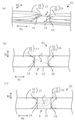
図5、6を用いて、図1に示すサーマルヘッドX1の電気抵抗層15、共通電極17、および個別電極19について詳細に説明する。   The electrical resistance layer 15, common electrode 17, and individual electrode 19 of the thermal head X1 shown in FIG. 1 will be described in detail with reference to FIGS.

帯状に設けられた電気抵抗層15上の一方側に共通電極17として機能する第2導電部12が設けられ、他方側に個別電極19として機能する第2導電部22が設けられている。第2導電部12と第2導電部22とは、所定の距離をあけて対向した状態で、電気抵抗層15上に設けられている。そして、第2導電部12、22は、それぞれ平面視して、矩形状をなしており、第2導電部12、22が設けられていない領域である発熱部9が、平面視して、矩形状をなしている。   A second conductive portion 12 that functions as the common electrode 17 is provided on one side of the electric resistance layer 15 provided in a band shape, and a second conductive portion 22 that functions as the individual electrode 19 is provided on the other side. The second conductive portion 12 and the second conductive portion 22 are provided on the electric resistance layer 15 in a state of facing each other with a predetermined distance. The second conductive portions 12 and 22 have a rectangular shape in plan view, and the heat generating portion 9 that is an area where the second conductive portions 12 and 22 are not provided is rectangular in plan view. It has a shape.

共通電極17として機能する第2導電部12上には、共通電極17として機能する第1導電部10が配置されている。同様に、個別電極19として機能する第2導電部22上には、個別電極19として機能する第1導電部20が配置されている。   On the second conductive portion 12 that functions as the common electrode 17, the first conductive portion 10 that functions as the common electrode 17 is disposed. Similarly, the first conductive portion 20 functioning as the individual electrode 19 is disposed on the second conductive portion 22 functioning as the individual electrode 19.

第1導電部10、20は、D2方向における中央部に、突出部14、24を有している。突出部14、24は、平面視して、円弧状をなしており、突出部14、24の最も発熱部9側に位置する部位が、第1導電部材10、20のD2方向において中央部に配置されている。   The 1st electroconductive parts 10 and 20 have the protrusion parts 14 and 24 in the center part in D2 direction. The protrusions 14 and 24 have an arc shape in plan view, and the portion of the protrusions 14 and 24 located closest to the heat generating part 9 is at the center in the D2 direction of the first conductive members 10 and 20. Has been placed.

図5(b)に示すように、突出部14、24は、発熱部9と所定の距離をあけて配置されている。その理由については後述するが、突出部10、20がD2方向に突出した状態で設けられているため、第1導電部10、20と発熱部9との距離は、D2方向の中央部にて最も近く、D2方向の両端部にて最も遠い構成となっている。   As shown in FIG. 5B, the protrusions 14 and 24 are arranged at a predetermined distance from the heat generating part 9. Although the reason will be described later, since the protrusions 10 and 20 are provided in a state protruding in the D2 direction, the distance between the first conductive parts 10 and 20 and the heat generating part 9 is at the center in the D2 direction. The closest configuration is the farthest at both ends in the D2 direction.

第1導電部10、20は、D3方向における厚みが、0.6〜2μmであることが好ましい。D3方向における厚みが0.6〜2μmであることにより、共通電極17または個別電極19として機能する際に、電気抵抗が高くなることを抑えることができる。また、第1導電部10、20は、D3方向における厚みが、0.6〜2μmであることから、D1方向における断面積が大きく、発熱部9の熱が、第1導電部10、20に熱伝導する際の熱抵抗が小さくすることができる。そのため、発熱部9の熱を共通電極17または個別電極19に熱伝導させることができる。   The first conductive portions 10 and 20 preferably have a thickness in the D3 direction of 0.6 to 2 μm. When the thickness in the D3 direction is 0.6 to 2 μm, it is possible to suppress an increase in electrical resistance when functioning as the common electrode 17 or the individual electrode 19. Further, since the first conductive portions 10 and 20 have a thickness in the D3 direction of 0.6 to 2 μm, the cross-sectional area in the D1 direction is large, and the heat of the heat generating portion 9 is transferred to the first conductive portions 10 and 20. The thermal resistance when conducting heat can be reduced. Therefore, the heat of the heat generating part 9 can be conducted to the common electrode 17 or the individual electrode 19.

第2導電部12、22は、それぞれ共通電極17または個別電極19として機能しており、D3方向における厚みが0.2〜0.5μmあることが好ましい。D3方向における厚みが0.2〜0.5μmであることから、図6(a)に示すように、D1方向における断面積を小さくすることができる。それにより、発熱部9の熱が、第2導電部12、22に熱伝導する際の熱抵抗を増加させることができ、発熱部9の熱が共通電極17または個別電極19に熱伝導することを抑えることができる。   The second conductive portions 12 and 22 each function as the common electrode 17 or the individual electrode 19 and preferably have a thickness in the D3 direction of 0.2 to 0.5 μm. Since the thickness in D3 direction is 0.2-0.5 micrometer, as shown to Fig.6 (a), the cross-sectional area in D1 direction can be made small. Thereby, the heat resistance when the heat of the heat generating part 9 is conducted to the second conductive parts 12 and 22 can be increased, and the heat of the heat generating part 9 is conducted to the common electrode 17 or the individual electrode 19. Can be suppressed.

サーマルヘッドX1は、第1導電部10、20と発熱部9とを第2導電部12、22により接続するため、発熱部9の熱を共通電極17および個別電極19に熱伝導することを低減しつつ、共通電極17および個別電極19の電気抵抗が増大しない構成となっている。   Since the thermal head X1 connects the first conductive portions 10 and 20 and the heat generating portion 9 with the second conductive portions 12 and 22, the heat conduction of the heat of the heat generating portion 9 to the common electrode 17 and the individual electrode 19 is reduced. However, the electric resistance of the common electrode 17 and the individual electrode 19 is not increased.

第1導電部10、20、および第2導電部12、22は、上述した各種電極を形成する材料により作製することができる。また、第1導電部10、20、および第2導電部12、22の作製方法としては、薄膜形成技術あるいは厚膜形成技術を用いて作製することができる。   The 1st electroconductive parts 10 and 20 and the 2nd electroconductive parts 12 and 22 can be produced with the material which forms the various electrodes mentioned above. The first conductive parts 10 and 20 and the second conductive parts 12 and 22 can be manufactured using a thin film forming technique or a thick film forming technique.

サーマルヘッドX1の共通電極17および個別電極19の作製方法を例示すると、電気抵抗層15が設けられたヘッド基体3に、スパッタリングあるいは真空蒸着により第2導電部12、22を設ける。そして、第2導電部12、22上にスクリーン印刷等により第1導電部10、20を設ける。そして、フォトエッチング手法等により所定のパターンを形成することにより、共通電極17および個別電極19を作製することができる。なお、第2導電部12、22および第1導電部10、20を所定のパターンに印刷して作製してもよい。   Exemplifying a method for producing the common electrode 17 and the individual electrode 19 of the thermal head X1, the second conductive portions 12 and 22 are provided by sputtering or vacuum deposition on the head substrate 3 on which the electrical resistance layer 15 is provided. Then, the first conductive portions 10 and 20 are provided on the second conductive portions 12 and 22 by screen printing or the like. Then, the common electrode 17 and the individual electrode 19 can be produced by forming a predetermined pattern by a photoetching method or the like. The second conductive parts 12 and 22 and the first conductive parts 10 and 20 may be produced by printing them in a predetermined pattern.

また、第1導電部10、20と第2導電部12、22とを別材料により形成してもよい。例えば、第1導電部10、20を第2導電部12、22よりも熱伝導率の高い材料により形成してもよい。具体的には、例えば、主成分がアルミニウム(Al)の第2導電部12、22に含まれるチタン(Ti)、またはネオジウム(Nd)等の含有量を第1導電部10、20において少なくするまたは、非含有にすることで、第1導電部10、20の熱抵抗を下げることができる。   Further, the first conductive portions 10 and 20 and the second conductive portions 12 and 22 may be formed of different materials. For example, the first conductive parts 10 and 20 may be formed of a material having a higher thermal conductivity than the second conductive parts 12 and 22. Specifically, for example, the content of titanium (Ti) or neodymium (Nd) contained in the second conductive parts 12 and 22 whose main component is aluminum (Al) is reduced in the first conductive parts 10 and 20. Alternatively, the non-containment can reduce the thermal resistance of the first conductive parts 10 and 20.

サーマルヘッドによる熱記録は、短い時間でサーマルヘッドの発熱部にジュール熱を発生させる。時間が極めて短いので、一般的に、発熱部の中央部は周辺部よりも高温となる。つまり、図5におけるD2方向の両端部に比べて中央部における温度が高くなり、図5におけるD1方向の両端部に比べて中央部における温度が高くなる温度分布(以下、温度分布と称する場合がある)が生じる場合がある(図6bの一点鎖線を参照)。   Thermal recording with a thermal head generates Joule heat in the heat generating part of the thermal head in a short time. Since the time is extremely short, generally, the central part of the heat generating part is hotter than the peripheral part. That is, a temperature distribution in which the temperature in the center portion is higher than both end portions in the D2 direction in FIG. 5 and the temperature in the center portion is higher than both end portions in the D1 direction in FIG. 5 (hereinafter sometimes referred to as temperature distribution). May occur) (see dashed line in FIG. 6b).

それにより、この温度分布は、記録媒体と発熱部との接触領域にも反映され、記録媒体の画素形成領域の中央部は周辺部よりも温度が高くなる。そのため、D2方向の中央部の印字が両端部に比べて濃くなり、サーマルヘッド特有の発熱部ごとの濃度階調表現による印画方式の場合特に濃度ムラが生じやすく、サーマルヘッドの画素再現性が低下する場合があった。   Thereby, this temperature distribution is also reflected in the contact area between the recording medium and the heat generating part, and the temperature in the central part of the pixel forming area of the recording medium is higher than that in the peripheral part. For this reason, the printing at the center in the D2 direction is darker than both ends, and density unevenness is particularly likely to occur in the printing method using the density gradation expression for each heat generating part specific to the thermal head, and the pixel reproducibility of the thermal head is reduced. There was a case.

これに対して、サーマルヘッドX1によれば、平面視して、発熱部9が矩形状であるとともに、発熱部9と接続された共通電極17および個別電極19が、第1導電部10、20と、発熱部9と第1導電部10、20とを接続する第2導電部12、22とを有しており、第1導電部10、20は、D2方向における中央部に、発熱部9側に突出した突出部14、24が設けられていることから、図6(a)で示すように、D2方向における両端部に比べて中央部のD3方向の厚みを厚くすることができる。   On the other hand, according to the thermal head X1, the heat generating portion 9 has a rectangular shape in plan view, and the common electrode 17 and the individual electrode 19 connected to the heat generating portion 9 are connected to the first conductive portions 10 and 20. And the second conductive portions 12 and 22 that connect the heat generating portion 9 and the first conductive portions 10 and 20, and the first conductive portions 10 and 20 are located at the center in the D2 direction at the heat generating portion 9. Since the projecting portions 14 and 24 projecting to the side are provided, as shown in FIG. 6A, the thickness in the D3 direction of the central portion can be made thicker than both end portions in the D2 direction.

それにより、発熱部9から共通電極17および個別電極19への熱伝導に対する熱抵抗を、D2方向における両端部の熱抵抗よりも中央部の熱抵抗を低くすることができ、共通電極17および個別電極19のD2方向における中央部に、発熱部9に生じた熱を効率よく熱伝導させることができる。そのため、発熱部9のD2方向の中央部の温度を下げることができ、発熱部9の温度分布を、図6(b)の実線で示すように、均一に近づけることができる。   Thereby, the thermal resistance to the heat conduction from the heat generating part 9 to the common electrode 17 and the individual electrode 19 can be made lower than the thermal resistance at the both ends in the D2 direction. The heat generated in the heat generating portion 9 can be efficiently conducted to the central portion of the electrode 19 in the D2 direction. Therefore, the temperature of the central portion in the D2 direction of the heat generating portion 9 can be lowered, and the temperature distribution of the heat generating portion 9 can be made closer to uniform as shown by the solid line in FIG.

それゆえ、D2方向の中央部の印字が両端部に比べて濃くなる可能性を低減することができ濃度ムラを低減し、サーマルヘッドX1の画素再現性を向上させることができる。   Therefore, it is possible to reduce the possibility that the printing at the center in the D2 direction is darker than both ends, reduce density unevenness, and improve the pixel reproducibility of the thermal head X1.

また、平面視して、発熱部9が矩形状をなしていることから、発熱部9により構成される1画素も、濃度階調表現における高濃度域において矩形状になすことができる。そのため、印字した際に画素間に隙間が生じる可能性を低減することができ、画素再現性を向上させることができる。   Further, since the heat generating portion 9 has a rectangular shape in plan view, one pixel constituted by the heat generating portion 9 can also be formed in a rectangular shape in a high density region in density gradation expression. Therefore, it is possible to reduce the possibility that a gap is generated between pixels when printing, and to improve pixel reproducibility.

さらに、第1導電部10、20は、D2方向における中央部に、発熱部9側に突出した突出部14、24が設けられていることから、発熱部9における保護膜25表面においても、第1導電部10、20および第2導電部12、22の形状が反映されるため、記録媒体(不図示)と発熱部9との接触性を向上させることができ、発熱部9の1画素を矩形状に近づけることができることから、さらにサーマルヘッドX1の濃度ムラを低減し、サーマルヘッドX1の画素再現性を向上させることができる。   Furthermore, since the first conductive portions 10 and 20 are provided with the protruding portions 14 and 24 protruding toward the heat generating portion 9 at the center in the D2 direction, the first conductive portions 10 and 20 are also provided on the surface of the protective film 25 in the heat generating portion 9. Since the shapes of the first conductive portions 10 and 20 and the second conductive portions 12 and 22 are reflected, the contact between the recording medium (not shown) and the heat generating portion 9 can be improved. Since it can be close to a rectangular shape, density unevenness of the thermal head X1 can be further reduced, and pixel reproducibility of the thermal head X1 can be improved.

また、第1導電部10、20の厚みが第2導電部12、22の厚みよりも厚いことから、発熱部9から共通電極17および個別電極19に多くの熱が熱伝導する可能性を低減することができ、サーマルヘッドX1の熱応答特性を向上させることができる。特に、D2方向における両端部において、発熱部9から共通電極17および個別電極19に熱伝導する熱を低減することができ、発熱部9の温度分布をさらに均一化することができる。   In addition, since the thickness of the first conductive portions 10 and 20 is thicker than the thickness of the second conductive portions 12 and 22, the possibility that a large amount of heat is conducted from the heat generating portion 9 to the common electrode 17 and the individual electrode 19 is reduced. It is possible to improve the thermal response characteristics of the thermal head X1. In particular, at both ends in the D2 direction, the heat conducted from the heat generating part 9 to the common electrode 17 and the individual electrode 19 can be reduced, and the temperature distribution of the heat generating part 9 can be made more uniform.

また、図6(b)の一点鎖線で示すように従来の発熱部の温度分布は、急峻に連続して変化しているが、サーマルヘッドX1は、第1導電部10、20の突出部14、24の外
周が、平面視して曲線をなしていることから、発熱部9からの熱をD2方向になだらかに熱伝導させることができ、図6(b)の実線で示すように発熱部9の温度分布をより均一に近づけることができる。それゆえ、D2方向の中央部の印字が両端部に比べて濃くなることを抑えることができ濃度ムラを低減し、サーマルヘッドX1の画素再現性を向上させることができる。
In addition, as shown by the alternate long and short dash line in FIG. 6B, the temperature distribution of the conventional heat generating portion changes steeply and continuously, but the thermal head X1 has the protruding portions 14 of the first conductive portions 10 and 20. , 24 is curved in plan view, so that heat from the heat generating portion 9 can be smoothly conducted in the direction D2, and the heat generating portion as shown by the solid line in FIG. 6B. The temperature distribution of 9 can be made more uniform. Therefore, it is possible to suppress the printing at the center in the D2 direction from becoming darker than both ends, reduce density unevenness, and improve the pixel reproducibility of the thermal head X1.

なお、サーマルヘッドX1においては、第1導電部10、20の厚みが第2導電部12、22の厚みよりも厚い構成を示したが、第1導電部10、20の厚みが第2導電部12、22の厚みよりも厚くなくてもよい。例えば、第1導電部10、20の厚みと第2導電部12、22の厚みが等しい場合においても、D2方向の中央部における厚みを両端部に比べて厚くすることができ、D2方向の両端部における熱抵抗を両端部に比べて低くすることができる。それにより、画素再現性の向上したサーマルヘッドX1とすることができる。   In the thermal head X1, the thickness of the first conductive portions 10 and 20 is greater than the thickness of the second conductive portions 12 and 22, but the thickness of the first conductive portions 10 and 20 is the second conductive portion. It may not be thicker than the thicknesses 12 and 22. For example, even when the thickness of the first conductive parts 10 and 20 and the thickness of the second conductive parts 12 and 22 are equal, the thickness in the center part in the D2 direction can be made larger than the both end parts. The thermal resistance at the part can be made lower than at both ends. Thereby, the thermal head X1 with improved pixel reproducibility can be obtained.

また、サーマルヘッドX1は、第1導電部10、20、の突出部14、24の外周が、平面視して曲線をなしている例を示したが、サーマルヘッドX1は、第1導電部10、20、の突出部14、24の外周が、平面視して曲線をなしていなくともよい。例えば、突出部14、24の外周が、三角形状、台形状、あるいは矩形状をなしていてもよい。   Moreover, although the thermal head X1 showed the example in which the outer periphery of the protrusion parts 14 and 24 of the 1st electroconductive part 10 and 20 has comprised the curve in planar view, the thermal head X1 shows the 1st electroconductive part 10 , 20, and the outer periphery of the protrusions 14 and 24 do not have to be curved in plan view. For example, the outer periphery of the protrusions 14 and 24 may have a triangular shape, a trapezoidal shape, or a rectangular shape.

さらに、突出部14、24がD2方向における両端部から中央部にかけて突出した例を示したが、突出部14、24がD2方向の中央部のみから突出していてもよい。その場合においても、発熱部9のD2方向の中央部の熱を第1導電部10、20に熱伝導させることができ、発熱部9の温度分布を均一化することができる。   Furthermore, although the example in which the protrusions 14 and 24 protrude from both ends in the D2 direction to the center is shown, the protrusions 14 and 24 may protrude only from the center in the D2 direction. Even in this case, the heat at the center of the heat generating part 9 in the D2 direction can be conducted to the first conductive parts 10 and 20, and the temperature distribution of the heat generating part 9 can be made uniform.

なお、平面視して、発熱部9が矩形状をなしているとは、製造誤差の範囲も含む概念である。   In addition, it is a concept including the range of a manufacturing error that the heat-emitting part 9 is carrying out the rectangular shape in planar view.

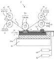
次に、本発明の一実施形態に係るサーマルプリンタZ形態について、図7を参照しつつ説明する。図7は、本実施形態のサーマルプリンタZの概略構成図である。   Next, a thermal printer Z configuration according to an embodiment of the present invention will be described with reference to FIG. FIG. 7 is a schematic configuration diagram of the thermal printer Z of the present embodiment.

図7に示すように、本実施形態のサーマルプリンタZは、上述のサーマルヘッドX1、搬送機構40、プラテンローラ50、電源装置60および制御装置70を備えている。サーマルヘッドX1は、サーマルプリンタZの筐体に設けられた取付部材80の取付面80aに取り付けられている。なお、このサーマルヘッドX1は、発熱部9の配列方向が、後述する記録媒体Pの搬送方向Sに直交する方向、言い換えると主走査方向であり、図7においては紙面に直交する方向に沿うようにして、取付部材80に取り付けられている。   As shown in FIG. 7, the thermal printer Z according to the present embodiment includes the thermal head X <b> 1, the transport mechanism 40, the platen roller 50, the power supply device 60, and the control device 70. The thermal head X1 is attached to an attachment surface 80a of an attachment member 80 provided in the casing of the thermal printer Z. In the thermal head X1, the arrangement direction of the heat generating portions 9 is a direction orthogonal to the conveyance direction S of the recording medium P, which will be described later, in other words, the main scanning direction, and in FIG. Thus, it is attached to the attachment member 80.

搬送機構40は、感熱紙、インクが転写される受像紙等の記録媒体Pを図7の矢印S方向に搬送して、サーマルヘッドX1の複数の発熱部9上、より詳細には保護膜25上に搬送するためのものであり、搬送ローラ43,45,47,49を有している。搬送ローラ43,45,47,49は、例えば、ステンレス等の金属からなる円柱状の軸体43a,45a,47a,49aを、ブタジエンゴム等からなる弾性部材43b,45b,47b,49bにより被覆して構成することができる。なお、図示しないが、記録媒体Pがインクが転写される受像紙等の場合は、記録媒体PとサーマルヘッドX1の発熱部9との間に、記録媒体Pとともにインクフィルムを搬送するようになっている。   The transport mechanism 40 transports the recording medium P such as thermal paper or image receiving paper onto which ink is transferred in the direction of arrow S in FIG. 7, and more specifically on the plurality of heat generating portions 9 of the thermal head X <b> 1. It is for carrying up, and has carrying rollers 43, 45, 47, and 49. The transport rollers 43, 45, 47, and 49 are formed by, for example, covering cylindrical shaft bodies 43a, 45a, 47a, and 49a made of metal such as stainless steel with elastic members 43b, 45b, 47b, and 49b made of butadiene rubber or the like. Can be configured. Although not shown, when the recording medium P is an image receiving paper to which ink is transferred, an ink film is conveyed together with the recording medium P between the recording medium P and the heat generating portion 9 of the thermal head X1. Yes.

プラテンローラ50は、記録媒体PをサーマルヘッドX1の発熱部9上に押圧するためのものであり、記録媒体Pの搬送方向Sに直交する方向に沿って延びるように配置され、記録媒体Pを発熱部9上に押圧した状態で回転可能となるように両端部が支持されている。プラテンローラ50は、例えば、ステンレス等の金属からなる円柱状の軸体50aを、
ブタジエンゴム等からなる弾性部材50bにより被覆して構成することができる。
The platen roller 50 is for pressing the recording medium P onto the heat generating portion 9 of the thermal head X1, and is disposed so as to extend along a direction orthogonal to the conveyance direction S of the recording medium P. Both ends are supported so as to be rotatable while being pressed on the heat generating portion 9. The platen roller 50 includes, for example, a cylindrical shaft body 50a made of a metal such as stainless steel.
It can be formed by covering with an elastic member 50b made of butadiene rubber or the like.

なお、本実施形態では、記録媒体Pの幅は、サーマルヘッドX1における蓄熱層13の隆起部13bの長さよりも大きくなっている。また、プラテンローラ50の長さ、より詳細には、弾性部材50bの長さは、サーマルヘッドX1における蓄熱層13の隆起部13bの長さよりも長くなっている。   In the present embodiment, the width of the recording medium P is larger than the length of the raised portion 13b of the heat storage layer 13 in the thermal head X1. Further, the length of the platen roller 50, more specifically, the length of the elastic member 50b is longer than the length of the raised portion 13b of the heat storage layer 13 in the thermal head X1.

電源装置60は、上記のようにサーマルヘッドX1の発熱部9を発熱させるための電流および駆動IC11を動作させるための電流を供給するためのものである。制御装置70は、上記のようにサーマルヘッドX1の発熱部9を選択的に発熱させるために、駆動IC11の動作を制御する制御信号を駆動IC11に供給するためのものである。   The power supply device 60 is for supplying a current for generating heat from the heat generating portion 9 of the thermal head X1 and a current for operating the drive IC 11 as described above. The control device 70 is for supplying a control signal for controlling the operation of the drive IC 11 to the drive IC 11 in order to selectively generate heat in the heat generating portion 9 of the thermal head X1 as described above.

本発明の実施形態に係るサーマルプリンタZは、図7に示すように、プラテンローラ50によって記録媒体PをサーマルヘッドX1の発熱部9上に押圧しつつ、搬送機構40によって記録媒体Pを発熱部9上に搬送しながら、電源装置60および制御装置70によって発熱部9を選択的に発熱させることで、記録媒体Pに所定の印画を行うことができる。なお、記録媒体Pが受像紙等の場合は、図示しないが記録媒体Pとともに搬送されるインクフィルムの昇華性インクを記録媒体Pに熱拡散することによって、記録媒体Pへの印画を行うことができる。
<第2の実施形態>
図8、9を用いて第2の実施形態に係るサーマルヘッドX2について説明する。
As shown in FIG. 7, the thermal printer Z according to the embodiment of the present invention presses the recording medium P onto the heat generating portion 9 of the thermal head X1 by the platen roller 50, while the recording mechanism P is heated by the transport mechanism 40. A predetermined printing can be performed on the recording medium P by selectively heating the heat generating portion 9 by the power supply device 60 and the control device 70 while being conveyed onto the recording medium 9. In the case where the recording medium P is an image receiving paper or the like, although not shown, the ink can be printed on the recording medium P by thermally diffusing the sublimation ink of the ink film conveyed with the recording medium P into the recording medium P. .
<Second Embodiment>
A thermal head X2 according to the second embodiment will be described with reference to FIGS.

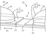
サーマルヘッドX2は、第1導電部10、20が、第1導電部10、20のD2方向における中央部に第1導電部10、20から上方に向けて延びる凸部16、26を有している。その他の構成は第1の実施形態に係るサーマルヘッドX1と同様であり、説明を省略する。   In the thermal head X2, the first conductive portions 10 and 20 have convex portions 16 and 26 that extend upward from the first conductive portions 10 and 20 at the center of the first conductive portions 10 and 20 in the D2 direction. Yes. Other configurations are the same as those of the thermal head X1 according to the first embodiment, and a description thereof will be omitted.

共通電極17側の第1導電部10および第2導電部12を用いて説明すると、第1導電部10がD2方向の中央部に凸部16を有しているため、図9(c)に示すように、D1方向に断面すると、D2方向の両端部と凸部16とが円弧状に接続されており、第1導電部10が半楕円形状をなしている。   If it demonstrates using the 1st electroconductive part 10 and the 2nd electroconductive part 12 by the side of the common electrode 17, since the 1st electroconductive part 10 has the convex part 16 in the center part of D2 direction, it will be in FIG.9 (c). As shown in the figure, when sectioned in the D1 direction, both end portions in the D2 direction and the convex portion 16 are connected in an arc shape, and the first conductive portion 10 has a semi-elliptical shape.

そのため、D3方向の第1導電部10の厚さが、D2方向に両端部から中央部に向けて厚くなる構成となっている。また、D2方向の両端部と凸部16とが円弧状に接続されていることから、D2方向の両端部における第1導電部10の厚さの変化率が、D2方向の中央部における第1導電部10の厚さの変化率よりも大きい構成となっている。   For this reason, the thickness of the first conductive portion 10 in the D3 direction is configured to increase from both end portions toward the central portion in the D2 direction. In addition, since both end portions in the D2 direction and the convex portion 16 are connected in an arc shape, the rate of change in the thickness of the first conductive portion 10 at both end portions in the D2 direction is the first rate at the center portion in the D2 direction. The configuration is larger than the rate of change of the thickness of the conductive portion 10.

第1導電部10の作製方法としては、第1の実施形態に係るサーマルヘッドX1のように厚膜形成技術により第1導電部10を作製した後、ディッピング、スタンプ、あるいはスプレー塗布等により凸部16を作製することができる。また、薄膜形成技術の場合、フォトエッチングプロセスでの、オーバーエッチング手法等により凸部16を作製することもできる。   As a manufacturing method of the first conductive portion 10, after forming the first conductive portion 10 by a thick film forming technique like the thermal head X1 according to the first embodiment, the convex portion is formed by dipping, stamping, spraying, or the like. 16 can be made. In the case of a thin film formation technique, the convex portion 16 can be produced by an overetching method or the like in a photoetching process.

サーマルヘッドX2は、第1導電部10、20が、図8のD2方向である、第1導電部10、20の幅方向における中央部の厚みが、第1導電部10、20の幅方向における両端部の厚みよりも厚いことから、共通電極17および個別電極19のD2方向の中央部における熱抵抗を両端部に向けてなだらかに低減するような構成とすることができる。   In the thermal head X2, the first conductive portions 10 and 20 are in the direction D2 in FIG. 8, and the thickness of the central portion in the width direction of the first conductive portions 10 and 20 is in the width direction of the first conductive portions 10 and 20. Since it is thicker than both end portions, it is possible to adopt a configuration in which the thermal resistance at the central portion in the D2 direction of the common electrode 17 and the individual electrode 19 is gradually reduced toward both end portions.

それにより、発熱部9に生じた熱を共通電極17および個別電極19のD2方向における中央部に、熱伝導させることができる。そのため、発熱部9のD2方向の中央部の温度
を下げることができ、発熱部9の温度分布を均一に近づけることができる。それゆえ、D2方向の中央部の印字が両端部に比べて濃くなる可能性を低減することができ濃度ムラを低減し、サーマルヘッドX2の画素再現性を向上させることができる。
Thereby, the heat generated in the heat generating part 9 can be thermally conducted to the central part in the D2 direction of the common electrode 17 and the individual electrode 19. Therefore, the temperature of the center part of the heat generating part 9 in the D2 direction can be lowered, and the temperature distribution of the heat generating part 9 can be made close to uniform. Therefore, it is possible to reduce the possibility that the printing at the center in the D2 direction is darker than both ends, reduce density unevenness, and improve the pixel reproducibility of the thermal head X2.

なお、サーマルヘッドX2においては、D2方向における中央部の厚みが、第1導電部10、20の幅方向における両端部の厚みよりもなだらかに厚くなる構成としたが、D2方向における中央部の厚みが、第1導電部10、20の幅方向における両端部の厚みよりも段階的に厚くなる構成としてもよい。なだらかに厚くなる構成とすることで、D2方向における熱抵抗を連続的に変化させることができ、発熱部9の温度分布をより均一に近づけることができる。また、D2方向における中央部の一部のみ厚くする構成としてもよい。   In the thermal head X2, the thickness of the central portion in the D2 direction is configured to be gradually thicker than the thickness of both end portions in the width direction of the first conductive portions 10 and 20, but the thickness of the central portion in the D2 direction is used. However, it is good also as a structure which becomes thick in steps rather than the thickness of the both ends in the width direction of the 1st electroconductive parts 10 and 20. FIG. By adopting a configuration in which the thickness is gradually increased, the thermal resistance in the D2 direction can be continuously changed, and the temperature distribution of the heat generating portion 9 can be made more uniform. Moreover, it is good also as a structure which thickens only a part of center part in D2 direction.

また、第1導電部10は、凸部16とD2方向における両端部とを円弧状に接続した例を示したが、D2方向における中央部にのみ凸部16を設ける構成としてもよい。
<第3の実施形態>
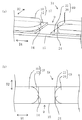
図10を用いて、第3の実施形態に係るサーマルヘッドX3について説明する。
Moreover, although the 1st electroconductive part 10 showed the example which connected the convex part 16 and the both ends in D2 direction in circular arc shape, it is good also as a structure which provides the convex part 16 only in the center part in D2 direction.
<Third Embodiment>
A thermal head X3 according to the third embodiment will be described with reference to FIG.

サーマルヘッドX3は、平面視して、共通電極17として機能する第1導電部10の突出部14の最も発熱部9側に突出している部位が、D2方向における中央部側より一端側に配置されており、個別電極19として機能する第1導電部20の突出部24の最も発熱部9側に突出している部位が、D2方向における中央部側より他端側に配置されている。その他の構成はサーマルヘッドX1と同様であり説明を省略する。なお、図10(b)に示す破線は、突出部14、24同士を結ぶ線分を示しており、図10(c)に示す一点鎖線は、発熱部9における等温線を示している。   In the thermal head X3, a portion of the protrusion 14 of the first conductive portion 10 that functions as the common electrode 17 that protrudes closest to the heat generating portion 9 is disposed on one end side from the center side in the direction D2. The portion of the protruding portion 24 of the first conductive portion 20 that functions as the individual electrode 19 that protrudes closest to the heat generating portion 9 is disposed on the other end side from the central portion side in the D2 direction. Other configurations are the same as those of the thermal head X1, and the description thereof is omitted. In addition, the broken line shown in FIG.10 (b) has shown the line segment which connects the protrusion parts 14 and 24, and the dashed-dotted line shown in FIG.10 (c) has shown the isothermal line in the heat generating part 9. FIG.

ここで、サーマルヘッドX1のように、平面視して、共通電極17として機能する第1導電部10の突出部14の最も発熱部9側に突出している部位が、D2方向における中央部に配置されており、個別電極19として機能する第1導電部20の突出部24の最も発熱部9側に突出している部位が、D2方向における中央部に配置されている場合、発熱部9における等温線は、突出部14、24を結ぶ線分上に、発熱部9の中心Iを中心として楕円形状となる。   Here, as in the case of the thermal head X1, the portion of the protrusion 14 of the first conductive portion 10 that functions as the common electrode 17 that protrudes closest to the heat generating portion 9 in plan view is disposed at the center in the D2 direction. When the portion of the protruding portion 24 of the first conductive portion 20 that functions as the individual electrode 19 that protrudes closest to the heat generating portion 9 is disposed at the center in the D2 direction, the isotherm in the heat generating portion 9 Is in the shape of an ellipse centered on the center I of the heat generating part 9 on the line segment connecting the protruding parts 14, 24.

これに対して、サーマルヘッドX3の発熱部9の等温線は、突出部14、24に発熱部9の熱が熱伝導することにより、図10(c)に示すように、発熱部9の中心Iを中心とした平行四辺形状となる。   On the other hand, the isotherm of the heat generating part 9 of the thermal head X3 is the center of the heat generating part 9 as shown in FIG. A parallelogram shape with I as the center.

そのため、発熱部9の温度分布を画素の形状である矩形状に近づけることができるため、画素間に隙間が生じる可能性を低減することができ、画素再現性を向上させることができる。   Therefore, since the temperature distribution of the heat generating part 9 can be made close to a rectangular shape that is the shape of the pixel, the possibility of a gap between the pixels can be reduced, and the pixel reproducibility can be improved.

さらに、共通電極17における第1導電部10の突出部14が、図10におけるD2方向である第1導電部10、20の幅方向における中央部より一端側に配置されており、他方の個別電極19における第1導電部20の突出部24が、図10におけるD2方向である第1導電部10、20の幅方向における中央部より他端側に配置されていることから、記録媒体(不図示)と発熱部9との接触性を向上させることができ、さらにサーマルヘッドX3のスティッキング現象等による濃度ムラを低減し、サーマルヘッドX3の画素再現性を向上させることができる。   Further, the protruding portion 14 of the first conductive portion 10 in the common electrode 17 is disposed at one end side from the central portion in the width direction of the first conductive portions 10 and 20 that is the D2 direction in FIG. 19, the protrusion 24 of the first conductive portion 20 is disposed on the other end side from the central portion in the width direction of the first conductive portions 10 and 20, which is the D2 direction in FIG. ) And the heat generating portion 9 can be improved, density unevenness due to the sticking phenomenon of the thermal head X3 can be reduced, and pixel reproducibility of the thermal head X3 can be improved.

また、サーマルヘッドX3は、平面視して、共通電極17の第1導電部10と、個別電極19の第1導電部20とが、発熱部9の中心(図10(b)で示すI)に対して、点対
称な構成となっている。
Further, in the thermal head X3, in plan view, the first conductive portion 10 of the common electrode 17 and the first conductive portion 20 of the individual electrode 19 are the center of the heat generating portion 9 (I shown in FIG. 10B). In contrast, the configuration is point-symmetric.

そのため、突出部14、24の同士を接続する線分が発熱部9の中心Iを通ることとなり、発熱部9の中心Iの温度を低下させることができる。それゆえ、平面視して、共通電極17の第1導電部10と、個別電極19の第1導電部20とが、発熱部9の中心に対して、点対称であることが好ましい。   Therefore, the line segment connecting the protrusions 14 and 24 passes through the center I of the heat generating part 9, and the temperature of the center I of the heat generating part 9 can be lowered. Therefore, the first conductive portion 10 of the common electrode 17 and the first conductive portion 20 of the individual electrode 19 are preferably point-symmetric with respect to the center of the heat generating portion 9 in plan view.

なお、サーマルヘッドX3では、突出部14、24の外周をどちらも曲線により形成した例を示したが、突出部14、24の外周をどちらも平面視して、直線により形成してもよく、平面視して、直線および曲線により形成してもよい。その場合においても、発熱部9の温度分布を均一に近づけることができる。対称性あるいは発熱部9の温度分布の均一化のために、突出部14、24の外周をどちらも平面視して曲線により形成することが好ましい。
<第4の実施形態>
図11を用いて第4の実施形態に係るサーマルヘッドX4は、第1導電部10、20の
突出部14、24が、発熱部9に隣接して設けられている。その他の構成はサーマルヘッドX1と同様である。
In the thermal head X3, an example in which the outer peripheries of the protrusions 14 and 24 are both formed by curves is shown, but the outer peripheries of the protrusions 14 and 24 may both be formed by straight lines in plan view. You may form by a straight line and a curve in planar view. Even in that case, the temperature distribution of the heat generating portion 9 can be made to be uniform. In order to make symmetry or to make the temperature distribution of the heat generating part 9 uniform, it is preferable to form the outer circumferences of the protrusions 14 and 24 in a curved line in plan view.
<Fourth Embodiment>
In the thermal head X4 according to the fourth embodiment with reference to FIG. 11, the protruding portions 14 and 24 of the first conductive portions 10 and 20 are provided adjacent to the heat generating portion 9. Other configurations are the same as those of the thermal head X1.

サーマルヘッドX4は、第1導電部10、20の突出部14、24が、発熱部9に隣接
して設けられている。そのため、D2方向における中央部の発熱部9の熱を第1導電部10、20に効率よく伝熱させることができる。それにより、発熱部9の温度分布を均一に近づけることができる。
In the thermal head X 4, the protrusions 14 and 24 of the first conductive parts 10 and 20 are provided adjacent to the heat generating part 9. Therefore, the heat of the heat generating part 9 at the center in the D2 direction can be efficiently transferred to the first conductive parts 10 and 20. As a result, the temperature distribution of the heat generating portion 9 can be made closer to uniform.

また、D2方向における両端部は第2導電部12、22により第1導電部10、20と発熱部9とが接続されることになるため、D2方向における発熱部9の熱を第1導電部10、20とが奪う可能性を低減することができる。それにより、発熱部9の温度分布を均一に近づけることができる。   Moreover, since the 1st electroconductive parts 10 and 20 and the heat generating part 9 will be connected to the both ends in D2 direction by the 2nd electroconductive parts 12 and 22, the heat | fever of the heat generating part 9 in D2 direction will be 1st electroconductive part. The possibility of taking 10 and 20 can be reduced. As a result, the temperature distribution of the heat generating portion 9 can be made closer to uniform.

なお、サーマルヘッドX4においては、共通電極17の第1導電部10の突出部14および個別電極19の第1導電部20の突出部24がどちらも、発熱部9に隣接して設けた例を示したが、どちらか一方のみが隣接する構成としてもよい。その場合においても、発熱部9の温度分布を均一に近づけることができる。対称性あるいは発熱部9の温度分布の均一化のために、突出部14、24をどちらも発熱部9に隣接されることが好ましい。   In the thermal head X4, an example in which the protruding portion 14 of the first conductive portion 10 of the common electrode 17 and the protruding portion 24 of the first conductive portion 20 of the individual electrode 19 are both provided adjacent to the heat generating portion 9 is provided. Although shown, only one of them may be adjacent. Even in that case, the temperature distribution of the heat generating portion 9 can be made to be uniform. In order to make symmetry or to make the temperature distribution of the heat generating part 9 uniform, it is preferable that both the protrusions 14 and 24 are adjacent to the heat generating part 9.

以上、本発明の一実施形態について説明したが、本発明は上記実施形態に限定されるものではなく、その趣旨を逸脱しない限りにおいて種々の変更が可能である。例えば、実施形態X1〜X4を任意に組み合わせてもよい。   As mentioned above, although one Embodiment of this invention was described, this invention is not limited to the said embodiment, A various change is possible unless it deviates from the meaning. For example, the embodiments X1 to X4 may be arbitrarily combined.

例えば、第2導電部12、22上に第1導電部10、20を設けた例を示したが、これに限定されるものではない。第1導電部10、20上に第2導電部12、22を設けた構成としてもよい。この場合も、第1導電部10、20を上述したスパッタリング等の薄膜形成技術により、0.6〜2ミクロン厚の導電層を形成した後に、フォトエッチングプロセスを経て、さらに同様にスパッタリング等の薄膜形成技術により0.2〜0.5ミクロンの導電層を形成すればよい。なお、第1導電部10、20および第2導電部12、22を一体的に設けて、フォトエッチングプロセスにて、第1導電部としての突出部を形成してもよい。その場合においても、発熱部9の温度分布を均一に近づけることができる。   For example, although the example which provided the 1st electroconductive parts 10 and 20 on the 2nd electroconductive parts 12 and 22 was shown, it is not limited to this. The second conductive portions 12 and 22 may be provided on the first conductive portions 10 and 20. Also in this case, after forming the conductive layer having a thickness of 0.6 to 2 microns on the first conductive parts 10 and 20 by the above-described thin film formation technique such as sputtering, a thin film such as sputtering is similarly obtained through a photoetching process. A conductive layer of 0.2 to 0.5 microns may be formed by a forming technique. In addition, the 1st electroconductive part 10 and 20 and the 2nd electroconductive part 12 and 22 may be provided integrally, and the protrusion part as a 1st electroconductive part may be formed in a photo-etching process. Even in that case, the temperature distribution of the heat generating portion 9 can be made to be uniform.

また、最初に、第1導電部10、20を蓄熱層の形成された基板上に従来周知の薄膜パターン形成技術(スパッタリングおよびフォトエッチング手法等による技術)にて形成した後、電気抵抗層15および第2導電部12、22を、同じく従来周知の薄膜パターン形
成技術にて形成してもよい。このように作製すると、第1導電部10、20、電気抵抗層15、および第2導電部12、22の順で積層されることとなる。このような場合においても、発熱部9の温度分布を均一に近づけることができる。
First, after the first conductive portions 10 and 20 are formed on the substrate on which the heat storage layer is formed by a conventionally well-known thin film pattern forming technique (technique based on sputtering and photoetching techniques), the electric resistance layer 15 and The second conductive parts 12 and 22 may also be formed by a conventionally well-known thin film pattern forming technique. When manufactured in this manner, the first conductive portions 10 and 20, the electric resistance layer 15, and the second conductive portions 12 and 22 are stacked in this order. Even in such a case, the temperature distribution of the heat generating portion 9 can be made closer to uniform.

上記実施形態のサーマルヘッドX1〜4では、保護膜25が、電気絶縁層、封止層および耐摩耗層の3つの層を積層した積層体によって形成されているが、保護膜25の積層構成はこれに限定されるものではない。例えば、図示しないが、電気絶縁層と封止層との間や、封止層と耐摩耗層との間に他の層が介在していてもよい。   In the thermal heads X1 to X4 of the above embodiment, the protective film 25 is formed by a laminated body in which three layers of an electric insulating layer, a sealing layer, and an abrasion resistant layer are laminated. It is not limited to this. For example, although not shown, other layers may be interposed between the electrical insulating layer and the sealing layer, or between the sealing layer and the wear-resistant layer.

上記実施形態のサーマルヘッドX1〜4では、例えば、サーマルヘッドX1のように、蓄熱層13は、下地部13a上にこの下地部13aから部分的に隆起する隆起部13bを設けることによって、基板7上で部分的に隆起する隆起部が形成されているが、蓄熱層13の構成はこれに限定されるものではない。例えば、下地部13aを設けず、隆起部13bのみで蓄熱層13が構成されていてもよい。   In the thermal heads X1 to X4 of the above-described embodiment, for example, as in the thermal head X1, the heat storage layer 13 is provided with a raised portion 13b partially raised from the base portion 13a on the base portion 13a. Although the raised part which protrudes partially above is formed, the structure of the thermal storage layer 13 is not limited to this. For example, the heat storage layer 13 may be configured by only the raised portion 13b without providing the base portion 13a.

上記実施形態のサーマルヘッドX1〜4では、例えば、図1〜図4に示すように、下地部13aと隆起部13bとを有する蓄熱層13が基板7上に形成されているがこれに限定されるものではない。例えば、隆起部13bを設けず、蓄熱層13が下地部13aのみで構成されていてもよい。   In the thermal heads X1 to X4 of the above embodiment, for example, as shown in FIGS. 1 to 4, the heat storage layer 13 having the base portion 13a and the raised portion 13b is formed on the substrate 7, but the present invention is not limited thereto. It is not something. For example, the heat storage layer 13 may be composed of only the base portion 13a without providing the raised portion 13b.

なお、サーマルヘッドX1を用いたサーマルプリンタZの例について説明したが、このサーマルヘッドX1に代えて、サーマルヘッドX2〜X4のいずれかを用いてサーマルプリンタZを構成してもよい。   In addition, although the example of the thermal printer Z using the thermal head X1 was demonstrated, it may replace with this thermal head X1 and you may comprise the thermal printer Z using either thermal head X2-X4.

X1〜4 サーマルヘッド
Z サーマルプリンタ
1 放熱体
3 ヘッド基体
5 フレキシブルプリント配線板
7 基板
9 発熱部
10、20 第1導電部
12、22 第2導電部
13 蓄熱層
13b 隆起部
14、24 突出部
15 電気抵抗層
16、26 凸部
17 共通電極
19 個別電極
X1-4 Thermal Head Z Thermal Printer 1 Heat Dissipator 3 Head Base 5 Flexible Printed Circuit Board 7 Substrate 9 Heating Part 10, 20 First Conductive Part 12, 22 Second Conductive Part 13 Heat Storage Layer 13b Raised Part 14, 24 Protruding Part 15 Electric resistance layer 16, 26 Convex portion 17 Common electrode 19 Individual electrode

Claims (7)

複数の発熱部と、
該発熱部と接続された一対の電極と、を備えるサーマルヘッドにおいて、
平面視して、前記発熱部は、矩形状をなしており、
前記電極は、第1導電部と、前記発熱部と前記第1導電部とを接続する第2導電部とを有しており、
前記第1導電部は、該第1導電部の幅方向における中央部に、前記発熱部側に突出した突出部が設けられており、
該突出部は、前記発熱部と離間して配置されていることを特徴とするサーマルヘッド。
A plurality of heat generating parts;
In a thermal head comprising a pair of electrodes connected to the heat generating part,
In plan view, the heat generating part has a rectangular shape,
The electrode has a first conductive part, and a second conductive part that connects the heat generating part and the first conductive part,
The first conductive portion is provided with a protruding portion protruding toward the heat generating portion at a central portion in the width direction of the first conductive portion ,
The thermal head is characterized in that the projecting portion is disposed apart from the heat generating portion .
前記第1導電部は、前記発熱部と離間して配置されている、請求項1に記載のサーマルヘッド。 The thermal head according to claim 1, wherein the first conductive portion is disposed apart from the heat generating portion . 前記第1導電部は、該第1導電部の幅方向における中央部の厚みが、前記第1導電部の幅方向における両端部の厚みよりも厚い、請求項1または2に記載のサーマルヘッド。   3. The thermal head according to claim 1, wherein the first conductive portion has a thickness of a central portion in the width direction of the first conductive portion that is thicker than thicknesses of both end portions in the width direction of the first conductive portion. 前記突出部の外周が、平面視して曲線をなしている、請求項1乃至3のいずれかに記載のサーマルヘッド。   The thermal head according to any one of claims 1 to 3, wherein an outer periphery of the protruding portion is curved in plan view. 一方の前記電極における前記第1導電部の前記突出部が、前記第1導電部の幅方向における中央部より一端側に配置されており、
他方の前記電極における前記第1導電部の前記突出部が、前記第1導電部の幅方向における中央部より他端側に配置されている、請求項1乃至4のいずれかに記載のサーマルヘッド。
The protruding portion of the first conductive portion in one of the electrodes is disposed on one end side from the central portion in the width direction of the first conductive portion,
5. The thermal head according to claim 1, wherein the projecting portion of the first conductive portion of the other electrode is disposed on the other end side from the center portion in the width direction of the first conductive portion. .
一方の前記電極における前記第1導電部の前記突出部と、他方の前記電極における前記第1導電部の前記突出部とが、前記発熱部の中心に対して点対称である、請求項5に記載のサーマルヘッド。   6. The protrusion of the first conductive part in one of the electrodes and the protrusion of the first conductive part in the other electrode are point-symmetric with respect to the center of the heat generating part. The thermal head described. 請求項1乃至6のいずれかに記載のサーマルヘッドと、前記発熱部上に記録媒体を搬送する搬送機構と、前記発熱部上に記録媒体を押圧するプラテンローラとを備えることを特徴とするサーマルプリンタ。   A thermal head comprising: the thermal head according to claim 1; a transport mechanism that transports a recording medium onto the heat generating portion; and a platen roller that presses the recording medium onto the heat generating portion. Printer.
JP2011167164A 2011-07-29 2011-07-29 Thermal head and thermal printer equipped with the same Active JP5840887B2 (en)

Priority Applications (1)

Application Number Priority Date Filing Date Title
JP2011167164A JP5840887B2 (en) 2011-07-29 2011-07-29 Thermal head and thermal printer equipped with the same

Applications Claiming Priority (1)

Application Number Priority Date Filing Date Title
JP2011167164A JP5840887B2 (en) 2011-07-29 2011-07-29 Thermal head and thermal printer equipped with the same

Publications (2)

Publication Number Publication Date
JP2013028136A JP2013028136A (en) 2013-02-07
JP5840887B2 true JP5840887B2 (en) 2016-01-06

Family

ID=47785664

Family Applications (1)

Application Number Title Priority Date Filing Date
JP2011167164A Active JP5840887B2 (en) 2011-07-29 2011-07-29 Thermal head and thermal printer equipped with the same

Country Status (1)

Country Link
JP (1) JP5840887B2 (en)

Families Citing this family (1)

* Cited by examiner, † Cited by third party
Publication number Priority date Publication date Assignee Title
CN113597373B (en) * 2019-03-26 2023-02-03 京瓷株式会社 Thermal head and thermal printer

Family Cites Families (4)

* Cited by examiner, † Cited by third party
Publication number Priority date Publication date Assignee Title
JPS56121779A (en) * 1980-02-29 1981-09-24 Toshiba Corp Thermal head
JPH03246066A (en) * 1990-02-26 1991-11-01 Toshiba Corp Thermal head
JP5044133B2 (en) * 2005-12-28 2012-10-10 京セラ株式会社 Thermal head and thermal printer
JP2011126025A (en) * 2009-12-15 2011-06-30 Seiko Instruments Inc Thermal head and printer

Also Published As

Publication number Publication date
JP2013028136A (en) 2013-02-07

Similar Documents

Publication Publication Date Title
JP5836825B2 (en) Thermal head and thermal printer equipped with the same
JP5128010B1 (en) Thermal head and thermal printer equipped with the same
WO2014051143A1 (en) Thermal head and thermal printer provided with same
JP6130510B2 (en) Thermal head and thermal printer equipped with the same
JP2014104715A (en) Thermal head and thermal printer equipped with the same
JP6584641B2 (en) Thermal head and thermal printer
JP5174287B1 (en) Thermal head and thermal printer equipped with the same
JP5840887B2 (en) Thermal head and thermal printer equipped with the same
JP2013028021A (en) Thermal head and thermal printer having the same
JP5964739B2 (en) Thermal head and thermal printer equipped with the same
JP2011245762A (en) Thermal head
JP2015003437A (en) Thermal head and thermal printer including the same
JP6290632B2 (en) Thermal head and thermal printer equipped with the same
JP2012030380A (en) Thermal head and thermal printer equipped with the same
JP6208564B2 (en) Thermal head and thermal printer
JP5780715B2 (en) Thermal head and thermal printer equipped with the same
JP5844550B2 (en) Thermal head and thermal printer equipped with the same
JP2012245711A (en) Thermal head and thermal printer with the same
JP6670654B2 (en) Thermal head and thermal printer
JP5918049B2 (en) Thermal head and thermal printer equipped with the same
JP6426541B2 (en) Thermal head and thermal printer
JP6199814B2 (en) Thermal head and thermal printer
JP5952134B2 (en) Thermal head and thermal printer equipped with the same
JP2014188983A (en) Thermal head and thermal printer provided with the same
JP2013176882A (en) Thermal head and thermal printer including the same

Legal Events

Date Code Title Description
A621 Written request for application examination

Free format text: JAPANESE INTERMEDIATE CODE: A621

Effective date: 20140317

A977 Report on retrieval

Free format text: JAPANESE INTERMEDIATE CODE: A971007

Effective date: 20150223

A131 Notification of reasons for refusal

Free format text: JAPANESE INTERMEDIATE CODE: A131

Effective date: 20150303

A521 Written amendment

Free format text: JAPANESE INTERMEDIATE CODE: A523

Effective date: 20150507

TRDD Decision of grant or rejection written
A01 Written decision to grant a patent or to grant a registration (utility model)

Free format text: JAPANESE INTERMEDIATE CODE: A01

Effective date: 20151013

A61 First payment of annual fees (during grant procedure)

Free format text: JAPANESE INTERMEDIATE CODE: A61

Effective date: 20151112

R150 Certificate of patent or registration of utility model

Ref document number: 5840887

Country of ref document: JP

Free format text: JAPANESE INTERMEDIATE CODE: R150