JP5813227B2 - Manufacturing method of electronic device - Google Patents
Manufacturing method of electronic device Download PDFInfo
- Publication number
- JP5813227B2 JP5813227B2 JP2014522103A JP2014522103A JP5813227B2 JP 5813227 B2 JP5813227 B2 JP 5813227B2 JP 2014522103 A JP2014522103 A JP 2014522103A JP 2014522103 A JP2014522103 A JP 2014522103A JP 5813227 B2 JP5813227 B2 JP 5813227B2
- Authority
- JP
- Japan
- Prior art keywords
- substrate
- layer
- metal layer
- electronic device
- metal
- Prior art date
- Legal status (The legal status is an assumption and is not a legal conclusion. Google has not performed a legal analysis and makes no representation as to the accuracy of the status listed.)
- Active
Links
Images


Classifications
-
- H—ELECTRICITY
- H01—ELECTRIC ELEMENTS
- H01C—RESISTORS
- H01C7/00—Non-adjustable resistors formed as one or more layers or coatings; Non-adjustable resistors made from powdered conducting material or powdered semi-conducting material with or without insulating material
- H01C7/008—Thermistors
-
- H—ELECTRICITY
- H01—ELECTRIC ELEMENTS
- H01C—RESISTORS
- H01C7/00—Non-adjustable resistors formed as one or more layers or coatings; Non-adjustable resistors made from powdered conducting material or powdered semi-conducting material with or without insulating material
- H01C7/04—Non-adjustable resistors formed as one or more layers or coatings; Non-adjustable resistors made from powdered conducting material or powdered semi-conducting material with or without insulating material having negative temperature coefficient
- H01C7/041—Non-adjustable resistors formed as one or more layers or coatings; Non-adjustable resistors made from powdered conducting material or powdered semi-conducting material with or without insulating material having negative temperature coefficient formed as one or more layers or coatings
-
- H—ELECTRICITY
- H01—ELECTRIC ELEMENTS
- H01C—RESISTORS
- H01C17/00—Apparatus or processes specially adapted for manufacturing resistors
-
- H—ELECTRICITY
- H01—ELECTRIC ELEMENTS
- H01C—RESISTORS
- H01C7/00—Non-adjustable resistors formed as one or more layers or coatings; Non-adjustable resistors made from powdered conducting material or powdered semi-conducting material with or without insulating material
- H01C7/10—Non-adjustable resistors formed as one or more layers or coatings; Non-adjustable resistors made from powdered conducting material or powdered semi-conducting material with or without insulating material voltage responsive, i.e. varistors
- H01C7/12—Overvoltage protection resistors
-
- H—ELECTRICITY
- H01—ELECTRIC ELEMENTS
- H01C—RESISTORS
- H01C7/00—Non-adjustable resistors formed as one or more layers or coatings; Non-adjustable resistors made from powdered conducting material or powdered semi-conducting material with or without insulating material
- H01C7/18—Non-adjustable resistors formed as one or more layers or coatings; Non-adjustable resistors made from powdered conducting material or powdered semi-conducting material with or without insulating material comprising a plurality of layers stacked between terminals
-
- Y—GENERAL TAGGING OF NEW TECHNOLOGICAL DEVELOPMENTS; GENERAL TAGGING OF CROSS-SECTIONAL TECHNOLOGIES SPANNING OVER SEVERAL SECTIONS OF THE IPC; TECHNICAL SUBJECTS COVERED BY FORMER USPC CROSS-REFERENCE ART COLLECTIONS [XRACs] AND DIGESTS
- Y10—TECHNICAL SUBJECTS COVERED BY FORMER USPC
- Y10T—TECHNICAL SUBJECTS COVERED BY FORMER US CLASSIFICATION
- Y10T29/00—Metal working
- Y10T29/49—Method of mechanical manufacture
- Y10T29/49002—Electrical device making
- Y10T29/49082—Resistor making
- Y10T29/49085—Thermally variable
Description
本発明は、たとえば静電気の放電に対する保護またはセンサに適用可能な電子デバイスの製造方法に関する。
The present invention is related to a manufacturing method applicable electronic device to protect or sensor, for example for the discharge of static electricity.
一般的に低電圧の電源および信号電圧で駆動される電子回路は、たとえば電圧入力接続端子に静電気の過電圧が印加されると、破損する可能性がある。この繊細な回路部品をこのような過電圧から保護するために、静電気放電の保護のための保護素子が電圧入力接続端子に接続され、たとえば接地電位等の基準電位に対して高い静電気電圧をバイパスすることができる。 In general, an electronic circuit driven by a low-voltage power supply and a signal voltage may be damaged when, for example, an electrostatic overvoltage is applied to the voltage input connection terminal. In order to protect this delicate circuit component from such an overvoltage, a protection element for protection against electrostatic discharge is connected to the voltage input connection terminal to bypass a high electrostatic voltage with respect to a reference potential such as a ground potential. be able to.
静電気放電の保護回路として、たとえばSMD(表面実装技術)によって多層バリスタ(Vielschichtvaristoren)を用いることができる。回路基板またはLED(発光ダイオード)のハウジングへの組み込みには、できる限り薄いESD(Electro−Static−Discharge)保護素子を必要とする。しかしながら、構造部分高さすなわち層厚に関して、SMD多層バリスタでは従来製造技術的な限界があった。 As an electrostatic discharge protection circuit, for example, a multilayer varistor (Vielschichtvaristore) can be used by SMD (surface mount technology). Incorporation of a circuit board or LED (light emitting diode) into a housing requires an ESD (Electro-Static-Discharge) protective element as thin as possible. However, the SMD multilayer varistor has a limitation in the conventional manufacturing technology with respect to the structural part height, that is, the layer thickness.
非常に小さな構造部分高さ(Bauteilhohe)を備えたデバイスを製造することができる電子デバイス製造方法を提供することが望まれている。さらにこの方法で製造されたデバイスを提供することが望まれている。 It would be desirable to provide an electronic device manufacturing method capable of manufacturing devices with very small structural part heights (Bauteilhohe). It would further be desirable to provide devices manufactured by this method.
本発明による電子デバイスの製造方法は、表面とこの表面に対向した第1の基板面とを有するセラミック半導体基板を準備するステップを備え、この基板内には金属層が含まれている。この基板の基板面には、少なくとも2つの他の金属層が互いに別々に設けられている。この基板およびこれら他の金属層からなる構成体は焼結される。基板の第1の基板面の少なくとも2つの他の金属層の間に、保護層として電気絶縁層が設けられる。この少なくとも2つの他の金属層にはそれぞれ、化学プロセスを用いてコンタクト層が設けられる。この化学プロセスによって、この基板の材質は、基板の表面から、最大で基板内部に設けられた金属層まで除去される。ここで基板(10)内に設けられた金属層(40)は、少なくとも2つの部位(U1,U2)で分断され、少なくとも2つの他の金属層(210)は、基板(10)の第1の基板面(S10a)に設けられ、基板の第1の基板面(S10a)の第1の領域(B1)および第2の領域(B2)は、少なくとも2つの他の金属層(210)によって覆われておらず、化学プロセスによって、基板(10)の材質が、基板(10)の第1の基板面(S10a)の領域(B1,B2)でエッチングされる。 An electronic device manufacturing method according to the present invention includes a step of preparing a ceramic semiconductor substrate having a surface and a first substrate surface facing the surface, and a metal layer is included in the substrate. On the substrate surface of this substrate, at least two other metal layers are provided separately from each other. The substrate and the other metal layers are sintered. An electrical insulating layer is provided as a protective layer between at least two other metal layers on the first substrate surface of the substrate. Each of the at least two other metal layers is provided with a contact layer using a chemical process. By this chemical process, the material of the substrate is removed from the surface of the substrate up to a metal layer provided inside the substrate. Here, the metal layer (40) provided in the substrate (10) is divided at at least two portions (U1, U2), and at least two other metal layers (210) are the first of the substrate (10). The first region (B1) and the second region (B2) of the first substrate surface (S10a) of the substrate are covered with at least two other metal layers (210). The material of the substrate (10) is etched in the region (B1, B2) of the first substrate surface (S10a) of the substrate (10) by a chemical process.
このようにして、この基板内に含まれる金属層の上に設けられた基板の材質が犠牲層となり、この犠牲層は、コンタクト層の取付けの化学プロセスの際には既に、この化学プロセスに含まれる酸/溶剤によってエッチング除去される。これと同時に、第1の基板面のパッシベーションの無い部分では、基板材質に溝がエッチングされる。この第1の基板面のパッシベーションの無い部分は、この第1の面に取付けられた金属層および電気絶縁層で覆われていない。コンタクト層を取付けるための化学プロセスとして、たとえば無電解メッキ(stromloses Galvanisieren)があり、たとえばENIG(無電解ニッケル浸漬金メッキ;electroless Nickel immersion plating)、ENEPIG(無電解ニッケル、無電解パラジウム浸漬金メッキ;electroless Nickel, electroless Palladium immersion gold)、または電解液がエッチングの酸と溶剤であるような電解メッキを用いることができる。 In this way, the material of the substrate provided on the metal layer contained in the substrate becomes a sacrificial layer, and this sacrificial layer is already included in the chemical process in the chemical process of attaching the contact layer. Etched away with acid / solvent. At the same time, a groove is etched in the substrate material in the non-passivated portion of the first substrate surface. The non-passivated portion of the first substrate surface is not covered with the metal layer and electrical insulating layer attached to the first surface. Chemical processes for attaching the contact layer include, for example, electroless plating (stromloses Galvanisieren), such as ENIG (electroless nickel immersion gold plating), ENEPIG (electroless nickel, electroless palladium immersion gold plating; electroless Nickel). , electroless palladium immersion gold), or electroplating where the electrolyte is an etching acid and solvent.
次のエッチングプロセスでは、デバイスを基板から分離するために、溝がさらにエッチングされ、基板内に設けられた金属層まで犠牲層が剥ぎ取られる。この基板内の金属層は、エッチング停止層として機能し、この下にある基板の材質はこれ以上エッチングされない。この基板の材質内に設けられた金属層は、基板の第1の基板面の近傍で基板の材質の中へ導入されることができるので、本方法は小さな高さのデバイスの製造を可能とする。 In the next etching process, the trench is further etched and the sacrificial layer is stripped down to the metal layer provided in the substrate to separate the device from the substrate. The metal layer in the substrate functions as an etch stop layer and the underlying substrate material is not etched any further. Since the metal layer provided in the material of the substrate can be introduced into the material of the substrate in the vicinity of the first substrate surface of the substrate, this method enables the manufacture of a device with a small height. To do.
コンタクト間の電気絶縁層は保護層であり、この保護層は、デバイスの分離のための化学プロセスもしくはエッチングプロセスの際に、この電気絶縁層の下に設けられた基板材質がエッチングされることを阻止する。このコンタクト間に設けられる保護層は、たとえばガラス、窒化珪素(Si3N4)、炭化珪素(SiC)、酸化アルミニウム(Al2O3)またはポリマーなどの材質を含んでいる。コンタクト層は、個別の層として、たとえば銀で形成されてよい。代替として、このコンタクト層は、複数の部分層、たとえばニッケル、パラジウム、金または錫等を含む種々の金属類を含んでよい。 The electrical insulating layer between the contacts is a protective layer, and this protective layer is used to check that the substrate material provided under this electrical insulating layer is etched during a chemical process or an etching process for device isolation. Stop. The protective layer provided between the contacts includes a material such as glass, silicon nitride (Si 3 N 4 ), silicon carbide (SiC), aluminum oxide (Al 2 O 3 ), or polymer. The contact layer may be formed as a separate layer, for example silver. Alternatively, the contact layer may comprise a plurality of partial layers, for example various metals including nickel, palladium, gold or tin.
本発明による電子デバイスの製造方法の実施形態は、とりわけ、電極として機能する金属層と、150μmより薄い特に略50μmのコンタクト層との間の部品高さのESD保護デバイスまたはセラミックセンサを実現することを可能とする。この際、この電子デバイスは安価に製造でき、極めて薄い個々のチップやこれらのアレイの製造に用いることができる。 Embodiments of a method for manufacturing an electronic device according to the invention realize inter alia an ESD protection device or ceramic sensor with a component height between a metal layer functioning as an electrode and a contact layer of less than 150 μm, in particular approximately 50 μm. Is possible. In this case, the electronic device can be manufactured at a low cost, and can be used for manufacturing very thin individual chips and arrays thereof.
この方法で製造された電子デバイスは、第1の基板面を有するセラミック半導体基板を備え、この第1の基板面に少なくとも2つの互いに離間したコンタクトが設けられており、この第1の基板面に対向する第2の基板面は、金属層の上に設けられている。すべてのコンタクトはそれぞれ、基板の第1の基板面に設けられた、さらにもう1つの金属層と、このもう1つの金属層の上に設けられたコンタクト層とを備える。少なくとも2つのコンタクトの間には、電気絶縁層が設けられており、この少なくとも2つのコンタクトは、この電気絶縁層によって互いに電気的に絶縁されている。この電子デバイスは、金属層とそれぞれのコンタクトのコンタクト層との間で、最大150μmの部品高さおよび好ましくは50μmの部品高さを有する。 An electronic device manufactured by this method includes a ceramic semiconductor substrate having a first substrate surface, and at least two contacts that are spaced apart from each other are provided on the first substrate surface. The opposing second substrate surface is provided on the metal layer. Each contact comprises a further metal layer provided on the first substrate surface of the substrate and a contact layer provided on the other metal layer. An electrical insulating layer is provided between the at least two contacts, and the at least two contacts are electrically insulated from each other by the electrical insulating layer. The electronic device has a component height of up to 150 μm and preferably a component height of 50 μm between the metal layer and the contact layer of each contact.
電子デバイスの製造方法の実施形態およびこの方法によって製造可能な電子デバイスの実施形態が、以下に図を参照して例示的に説明される。
図1Aは電子デバイスの第1の実施形態を示し、この電子デバイスは、たとえば静電気保護用またはセンサとして使用可能である。この電子デバイスは、セラミック半導体基板10を備える。この基板10は、基板面S10aとこの基板面S10aに対向する基板面S10bとを備える。基板の材質には、基板面S10aとS10bとの間に金属層40が設けられている。この金属層40は、たとえば銀を含んでよい。基板面S10aには、少なくとも2つの互いに離間したコンタクト21および22が設けられている。これらののコンタクト21および22はそれぞれ、金属層210とコンタクト層220とを備える。これらのコンタクト21および22の金属層210はそれぞれ、基板10の基板面S10aに設けられている。これらのコンタクト21および22のコンタクト層220はそれぞれ、金属層210の上に設けられている。
FIG. 1A shows a first embodiment of an electronic device that can be used, for example, for electrostatic protection or as a sensor. The electronic device includes a
これらのコンタクト21および22の金属層210は、たとえば銀を含んでよい。コンタクト層220は、たとえばニッケルおよび/または金からなる材質を備えてよい。たとえば、コンタクト21および22のそれぞれのコンタクト層220は、部分層221と部分層222とを備えてよい。部分層221は金属層210の上に設けられてよく、部分層222はこの部分層221の上に設けられてよい。部分層221は、たとえばニッケルからなる材質を備えてよく、部分層222は、たとえば金からなる材質を備えてよい。
The
これらのコンタクト21および22の間には、基板10の基板面S10aに電気絶縁層30が設けられている。この電気絶縁層30は、コンタクト端子21および22の金属層210とを互いに分離し、これら2つのコンタクト21および22のコンタクト層220を互いに分離するように形成されている。この層30によって2つのコンタクト21および22は、電気的に互いに絶縁されている。この電気絶縁層30は、たとえばガラスからなる材質を含んでよい。
Between these
図1Bは、図1Aに示す電子デバイスの第1の実施形態の平面図を示す。コンタクト21および22、特にこれらのコンタクト21および22のそれぞれのコンタクト層220が示されているが、これらは電気絶縁層30によって互いに分離され、これにより電気的に互いに絶縁されている。
図1Aおよび1Bに示す第1の実施形態では、金属層40とコンタクト面220との間の電子デバイスの構造部分高さ(Bauteilhohe)Hは、50μmとなっている。デバイスの幅Bは、たとえば100μmであり、長さLは250μmであってよい。この際、これらのコンタクト層220はそれぞれ、長さL1が50μmであってよく、電気絶縁層30は、長さL2が150μmであってよい。
FIG. 1B shows a plan view of a first embodiment of the electronic device shown in FIG. 1A.
In the first embodiment shown in FIGS. 1A and 1B, the structural part height (Bauteilhohe) H of the electronic device between the
図2A〜2Fは、電子デバイスの製造方法の1つの実施形態を示す。この電子デバイスは静電気放電の保護用かまたはセンサとして使用可能である。表面O10およびこの表面O10に対向する基板面S10aを有するセラミック半導体基板10が準備され、この基板内に金属層40が含まれている。この基板10内に設けられた金属層40は、少なくとも2つの部位U1,U2で分断されている。これらの部位U1,U2の外側に設けられた金属層40の断片は、他のデバイスに属している。この金属層40は、表面O10もしくは基板の基板面S10aにほぼ平行に、基板内部に設けられている。この内部に金属層40を含む基板10は、ウェーハとして形成されることができる。図2Aに示す本発明の製造方法の第1の製造ステップでは、基板10の積層、積み重ねおよび押圧が行われる。
2A-2F illustrate one embodiment of a method for manufacturing an electronic device. This electronic device can be used for electrostatic discharge protection or as a sensor. A
さらに次の図2Bに示す製造ステップでは、このウェーハもしくは基板10は、基板面S10aで、少なくとも2つの金属層210のパターンが設けられており、これらは電子デバイスのコンタクト21および22の一部を形成している。ここでこれらの金属層210は、互いに距離を置いて基板面S10aに設けられている。これに加えて、たとえば銀からなる材質の薄い層を、基板面S10aの互いに離間した断片の上に設けてよい。これらの少なくとも2つの金属層210は、基板10の基板面S10aに設けられ、基板10の基板面S10aの領域B1および領域B2は、この少なくとも2つの他の金属層によって覆われていない。これらの領域B1およびB2は、投影して見ると部位U1およびU2の下に配置されている。領域B1およびB2の隣に、他のデバイスに属する金属層210が設けられている。これらの金属層210は、この下にある基板の材質の保護層を形成している。
Further, in the next manufacturing step shown in FIG. 2B, the wafer or
さらに次の図2Cに示す製造ステップでは、この基板10の構成体が、これに設けられた金属層パターン210と共に焼結される。
Further, in the next manufacturing step shown in FIG. 2C, the structure of the
図2Dは、さらに次の製造ステップを示す。このステップは、金属層210の間の基板面S10aの部分に保護層を取付ける。保護層としては、コンタクト21および22の金属層210の間に、たとえばガラスからなる材質の電気絶縁層30が付けられる。この電気絶縁層30は、上記の離間した金属層210の間で、基板10の基板面S10aの部分に直接設けられてよい。この際、この保護層30は、金属層210の断片の一部の上にも取付けられてよい。これらの領域B1およびB2は、この後も保護層で覆われないままとなる。
FIG. 2D shows a further next manufacturing step. This step attaches a protective layer to the portion of the substrate surface S10a between the metal layers 210. As the protective layer, an electrical insulating
図2Eに示すさらに次のステップでは、コンタクト21および22が完成され、ここでそれぞれの金属層210の上にコンタクト層220が取付けられる。さらに加えて、この金属層210の上に、たとえばニッケルおよび/または金からなる材質を取付けてもよい。たとえば、全ての金属層210のそれぞれの上に、まずニッケルを含む部分層が取付けられ、この部分層221の上に、続いて金を含む部分層222が取付けられてよい。金属層210へのコンタクト層220の取付けは、化学プロセスによって電流を用いずに行うことができる。
In the next step shown in FIG. 2E,
コンタクト層220を取付けるための、酸もしくは溶剤が関与する化学プロセスによって、このコンタクト層220の取り付けの際に、保護層の無い領域B1およびB2で、基板の材質がエッチングされる。この際、基板の基板面S10aで、上記の保護層の無い領域B1,B2から溝Gが基板にエッチングされる。このエッチングは、たとえば異方性で行われる。コンタクト層210を取付ける化学プロセスによって、基板の材質は、溝の表面OGまで除去される。基板10の材質は、領域B1およびB2において、この溝の表面が金属層210と金属層40との間に位置するようになるまで除去されてよい。基板面S10aの領域B0は、保護層として機能する金属層210および電気絶縁層30で覆われており、この領域B0の下では基板の材質のエッチングが阻止される。
The substrate material is etched in the regions B1 and B2 without the protective layer during the attachment of the
さらに基板の材質は、保護層の無い表面O10でも金属層40に向かってエッチングされる。表面O10および金属層40の間にある基板の材質は、犠牲層となり、コンタクト層の取り付けのための化学プロセスの際にに、表面O10から表面O10'まで除去される、最初の表面O10および金属層40の間の領域を当初の犠牲層の厚さとすると、この犠牲層の表面O10'は、コンタクト面220の取り付けのための化学プロセスの作用の後、この犠牲層の最初の表面O10と金属層40との間に位置されてよい。このようにしてコンタクト層220の取り付けのための化学プロセスの際に、金属層40より上の基板の層厚が除去される。
Further, the material of the substrate is etched toward the
図2Fは、ウェーハ10から電子デバイス1を分離する、さらに次の製造ステップを示す。ここでさらに次の、たとえば異方性のエッチングプロセスで、既にコンタクト面220の取り付けの化学プロセスで形成された領域B1およびB2の溝がさらにエッチングされ、金属層40の分断部U1およびU2の下の基板までが完全に除去される。ここで、化学プロセスの際にプリエッチングされた溝の表面OGから少なくとも金属層40までの基板の材質が除去されてよい。さらに、金属層40の上側にまだ存在する、犠牲層を形成するセラミック半導体の基板の材質は、金属層40までエッチング除去されてよい。この金属層40は、エッチング停止層として機能し、この下にある基板の材質はこれ以上エッチングされない。このようにして、ウェーハ集合体からデバイスが分離される。この分離は、エッチングの他に代替として、個々のデバイスをウェーハ集合体からチッピング(Ausbrechen)によって行われてよい。
FIG. 2F shows a further next manufacturing step for separating the electronic device 1 from the
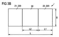
図3Aは電子デバイスのさらなる第2の実施形態の断面図を示し、この電子デバイスは、たとえば静電気保護用またはセンサとして使用可能である。この静電気用のデバイスは、セラミック半導体基板10を備える。このセラミック半導体基板10は、表面O10とこの表面O10に対向した基板面S10aとを備える。このセラミック半導体基板10の材質の内部には、金属層40が設けられている。この金属層40は、たとえば銀からなる材質を含んでよい。セラミック半導体基板10の基板面S10aには、互いに離間した少なくとも2つのコンタクト21および22が設けられている。これらのコンタクト21および22はともにそれぞれ、金属層210とコンタクト層220とを備える。それぞれのコンタクトの金属層210は、基板の基板面S10aに直接設けられ、たとえば銀からなる材質を含んでよい。
FIG. 3A shows a cross-sectional view of a further second embodiment of an electronic device, which can be used, for example, for electrostatic protection or as a sensor. The electrostatic device includes a
すべてのコンタクトのそれぞれのコンタクト層220は、それぞれの金属層210の上に設けられている。コンタクト層220は、たとえばニッケルおよび/または金からなる材質を備えてよい。このコンタクト層220は、たとえばそれぞれのコンタクトの金属層210の上に設けられた部分層221を備える。コンタクト層220のもう1つの部分層222は、この部分層221の上に設けられてよい。部分層221は、たとえばニッケルからなる材質を含んでよく、部分層222は、金からなる材質を含んでよい。
Each
コンタクト21および22の間には、図1Aおよび1Bに示す電子デバイスの変形例のように、電気絶縁層30は、保護層として設けられる。この電気絶縁層30は、上記の金属層210の間で、基板面S10aの部分に設けられてよい。この保護層30は、それぞれのコンタクト21および22の金属層210とコンタクト層220とを互いに電気的に絶縁するように形成されている。
Between the
図3Bは、図3Aに示す電子デバイスの第2の実施形態の平面図を示す。電子デバイスの下面には、コンタクト21および22が設けられ、詳細にはそれぞれのコンタクト21および22のコンタクト層220が設けられている。これらは、電気絶縁層30によって互いに電気的に絶縁されている。
FIG. 3B shows a plan view of a second embodiment of the electronic device shown in FIG. 3A.
図3Aおよび3Bに示す電子デバイス2は、たとえば表面O10とコンタクト層220との間で測った構造部分高さHが50μmで作製される。デバイスの幅Bは、100μmであり、長さLは250μmであってよい。この際、コンタクト21および22はそれぞれ、長さL1が50μmであってよく、電気絶縁層30は、長さL2が150μmであってよい。この第2の実施形態によるデバイスは、たとえば、最後の図2Eの製造ステップで、金属層40の上に設けられた基板10の犠牲層が金属層40まで完全に除去されずに製造されてよい。
The electronic device 2 shown in FIGS. 3A and 3B is manufactured, for example, with a structure portion height H measured between the surface O10 and the
図4Aは電子デバイスのさらなる第3の実施形態の断面図を示し、この電子デバイスは、たとえば静電気保護用またはセンサとして使用可能である。図1に示す実施形態と同様に、この電子デバイスはセラミック半導体基板10を備える。基板10の基板面S10aには、互いに離間した少なくとも2つのコンタクトが設けられている。図4Aに示す実施形態例では、電子デバイスは2つ以上のコンタクトのアレイを有して形成されている。このデバイスは、たとえば4つのコンタクト21,22,23および24を備えてよい。図4Aに示す断面図では、コンタクト21および22のみが見えている。
FIG. 4A shows a cross-sectional view of a further third embodiment of an electronic device, which can be used, for example, for electrostatic protection or as a sensor. Similar to the embodiment shown in FIG. 1, the electronic device comprises a
コンタクト21および22はともにそれぞれ、たとえば銀からなる層である金属層をそなえ、これらは基板面S10aで互いに離間して設けられている。さらにこれらのコンタクトは、それぞれコンタクト層220を備え、このコンタクト層は、それぞれのコンタクトの金属層210の上に設けられている。コンタクト層220は、ニッケルおよび/または金からなる材質を備えてよい。コンタクト層220は、たとえば部分層221および部分層222を備えてよい。この部分層221は、それぞれのコンタクトの金属層210の上に直接設けられている。部分層222は、それぞれのコンタクトの部分層221の上に設けられている。部分層221は、たとえばニッケルからなる材質を含んでよく、部分層222は、金からなる材質を含んでよい。
Each of the
これら2つのコンタクト21および22の間には、電気絶縁層30が設けられ、これによりコンタクト21と22とが、そしてそれぞれの金属層210とそれぞれのコンタクト層220とが電気的に互いに絶縁されている。この電気絶縁層30は、たとえば上記の金属層210の間で、基板10の基板面S10aの部分に直接設けられてよい。この電気絶縁層は、保護層となり、たとえばガラスからなる材質を備えてよい。
Between these two
図4Bは、図4Aに示す電子デバイスの第3の実施形態を平面図で示し、ここでコンタクト21,22,23および24と電気絶縁層30が示されている。図4Bに示すように、これらのコンタクト21,22,23,および24は、これらの間に設けられた電気絶縁層30によって、互いに高抵抗で分離され、すなわち互いに電気的に絶縁されている。
4B shows in plan view a third embodiment of the electronic device shown in FIG. 4A, where
図4Aおよび4Bに示す第3の実施形態では、金属層40とコンタクト面220との間の電子デバイス3の構造部分高さHは、50μmとなっている。電子デバイスの第1および第2の実施形態と異なり、この電子デバイスの第3の実施形態は、正方形の設置面を備える。この電子デバイスは、たとえば幅Bおよび長さLが250μmであってよい。この際、コンタクトはそれぞれ、幅B1が100μmであってよく、電気絶縁層は、幅B2が50μmであってよい。このコンタクトはそれぞれ、長さL1が50μmであってよく、電気絶縁層は、長さL2が150μmであってよい。
In the third embodiment shown in FIGS. 4A and 4B, the structural portion height H of the electronic device 3 between the
図5Aは、電子デバイスの第1の実施形態を保護層付きのセラミックチップの形態で示したものであり、このチップは、基板10、コンタクト21および22、これらの間に設けられた電気絶縁層30、およびさらなる金属層40を備える。このような構造によって、たとえば多層バリスタを有するデバイス、もしくはセンサとして使用可能な、多層NTC(負温度係数、Negative Temparature Coefficient)抵抗を有するデバイスを実現することができる。
FIG. 5A shows a first embodiment of an electronic device in the form of a ceramic chip with a protective layer, which comprises a
図5Bは、デバイスをバリスタとして実現したものを示すが、このデバイスは、たとえばESD保護デバイスとして使用可能である。多層バリスタとしての実施形態では、デバイスの基板10は、たとえば酸化亜鉛およびプラセオジムからなる材質、たとえばZnO(Pr)を含む。たとえば、基板10の材質として、プラセオジムがドープされた酸化亜鉛が用いられてよい。代替として、酸化亜鉛およびビスマスからなる材質、たとえばZnO(Bi)が用いられてもよい。コンタクト21および22はそれぞれ、基準電位、たとえば接地電位の印加のための接続端子を形成する。金属層40は、製造の際のエッチング停止層としての機能の他に、後にこのデバイスが動作する時に電流を輸送する電極としての機能を有する。この電流輸送電極40とコンタクト21との間に、セラミック半導体基板は電圧依存抵抗R1を形成する。金属層の形態の電流輸送電極40およびコンタクト22の間に、セラミック半導体基板10は、さらにもう1つの電圧依存抵抗R2を形成する。
FIG. 5B shows the device implemented as a varistor, which can be used, for example, as an ESD protection device. In an embodiment as a multi-layer varistor, the
図5は、基板の材質として負の温度係数を有する材質、たとえばNTC材料が用いられた場合の、デバイスの等価回路を示す。この場合、このデバイスはセラミックセンサとしてして使用することができる。基板10は、コンタクト21および22と金属層40との間に、それぞれ温度依存抵抗R3およびR4を形成する。これらのコンタクト21および22はそれぞれ、基準電位、たとえば接地電位の印加のための接続端子として用いることができる。金属層40は、このデバイスの動作の際に電流輸送電極として機能する。この金属層40とコンタクト21との間に、セラミック半導体基板10は温度依存抵抗R3を形成する。この金属層40とコンタクト22との間に、セラミック半導体基板10はさらなる温度依存抵抗R4を形成する。
FIG. 5 shows an equivalent circuit of a device when a material having a negative temperature coefficient, for example, an NTC material is used as the material of the substrate. In this case, the device can be used as a ceramic sensor. The
1,2,3 本発明によるデバイスの実施形態
10 セラミック半導体基板
21,22 コンタクト
30 電気絶縁層
40 金属層
210 金属層
220 コンタクト層
221,222 コンタクト層の部分層
R1,R2 電圧依存抵抗
R3,R4 温度依存抵抗
1, 2, 3
Claims (7)
表面(O10)とこの表面(O10)に対向する第1の基板面(S10a)とを有し、その内部に金属層(40)が含まれているセラミック半導体基板(10)を準備するステップと、
前記基板の前記基板面(S10a)に、互いに分離された少なくとも2つの他の金属層(210)を設けるステップと、
前記基板(10)と前記他の金属層(210)とからなる構成体を焼結するステップと、
前記基板面(S10a)に、前記少なくとも2つの他の金属層(210)の間に、電気絶縁層(30)を設けるステップと、
化学プロセスを用いて前記少なくとも2つの他の金属層(210)の上にそれぞれコンタクト層(220)を設けるステップであって、前記化学プロセスによって前記基板(10)の材質が、前記表面(O10)から、最大で基板内に設けられた金属層(40)まで除去されるステップと、
を備え、
前記基板(10)内に設けられた金属層(40)は、少なくとも2つの部位(U1,U2)で分断され、
前記少なくとも2つの他の金属層(210)は、基板(10)の第1の基板面(S10a)に設けられ、前記基板の前記第1の基板面(S10a)の第1の領域(B1)および第2の領域(B2)は、前記少なくとも2つの他の金属層(210)によって覆われておらず、
前記化学プロセスによって、前記基板(10)の材質が、前記基板(10)の前記第1の基板面(S10a)の領域(B1,B2)でエッチングされる、
ことを特徴とする方法。 An electronic device manufacturing method comprising:
Providing a ceramic semiconductor substrate (10) having a surface (O10) and a first substrate surface (S10a) opposite to the surface (O10), and including a metal layer (40) therein; ,
Providing at least two other metal layers (210) separated from each other on the substrate surface (S10a) of the substrate;
Sintering a structure comprising the substrate (10) and the other metal layer (210);
Providing an electrical insulating layer (30) between the at least two other metal layers (210) on the substrate surface (S10a);
Providing a contact layer (220) on each of the at least two other metal layers (210) using a chemical process, wherein the material of the substrate (10) is changed to the surface (O10) by the chemical process; To a maximum of the metal layer (40) provided in the substrate,
Equipped with a,
The metal layer (40) provided in the substrate (10) is divided at at least two parts (U1, U2),
The at least two other metal layers (210) are provided on the first substrate surface (S10a) of the substrate (10), and the first region (B1) of the first substrate surface (S10a) of the substrate. And the second region (B2) is not covered by the at least two other metal layers (210),
By the chemical process, the material of the substrate (10) is etched in the regions (B1, B2) of the first substrate surface (S10a) of the substrate (10).
A method characterized by that.
前記電子デバイス(1,2,3)の前記基板(10)の材質からの分離は、前記化学プロセスの後のエッチングプロセスで行われることを特徴とする方法。 The method of claim 1 , wherein
Separation of the electronic device (1, 2, 3) from the material of the substrate (10) is performed by an etching process after the chemical process.
前記基板(10)の、前記少なくとも2つの他の金属層(210)と前記電気絶縁層(30)とで覆われた領域(B0)での前記基板の材質のエッチングが阻止されることを特徴とする方法。 The method according to claim 1 or 2 , wherein
Etching of the material of the substrate in the region (B0) covered with the at least two other metal layers (210) and the electrical insulating layer (30) of the substrate (10) is prevented. And how to.
前記電子デバイス(1,2,3)の、前記基板(10)内に設けられた金属層(40)と前記コンタクト層(220)との間の構造部分高さが最大150μm、好ましくは50μmとなるように、前記基板内の前記金属層(40)が配設されることを特徴とする方法。 The method of claim 3 , wherein
Before SL electronic device (1,2,3), wherein the structural portion height up to 150μm between the substrate (10) metal layers provided in (40) and said contact layer (220), preferably 50μm The method according to claim 1, characterized in that the metal layer (40) in the substrate is disposed .
前記セラミック半導体基板(10)は、酸化亜鉛およびプラセオジムからなる材質または負の温度係数を有する材質を含むことを特徴とする方法。 The method according to any one of claims 1 to 4 ,
The method according to claim 1, wherein the ceramic semiconductor substrate (10) comprises a material comprising zinc oxide and praseodymium or a material having a negative temperature coefficient.
前記絶縁層(30)は、ガラスまたは窒化珪素または炭化珪素または酸化アルミニウムまたはポリマーからなる材質を含み、前記金属層(40)および前記他の金属層(210)は、銀からなる材質を含むことを特徴とする方法。 The method according to any one of claims 1 to 5 ,
The insulating layer (30) includes a material made of glass, silicon nitride, silicon carbide, aluminum oxide, or a polymer, and the metal layer (40) and the other metal layer (210) include a material made of silver. A method characterized by.
前記コンタクト層(220)は、ニッケルおよび/または金,および/またはパラジウム,および/または錫,および/または銀からなる材質を含むことを特徴とする方法。 The method according to any one of claims 1 to 6 ,
The contact layer (220) comprises a material comprising nickel and / or gold, and / or palladium, and / or tin, and / or silver.
Applications Claiming Priority (3)
| Application Number | Priority Date | Filing Date | Title |
|---|---|---|---|
| DE102011109007A DE102011109007A1 (en) | 2011-07-29 | 2011-07-29 | Method for producing an electrical component and an electrical component |
| DE102011109007.3 | 2011-07-29 | ||
| PCT/EP2012/064726 WO2013017531A1 (en) | 2011-07-29 | 2012-07-26 | Method for producing an electrical component and electrical component |
Publications (2)
| Publication Number | Publication Date |
|---|---|
| JP2014524154A JP2014524154A (en) | 2014-09-18 |
| JP5813227B2 true JP5813227B2 (en) | 2015-11-17 |
Family
ID=46581984
Family Applications (1)
| Application Number | Title | Priority Date | Filing Date |
|---|---|---|---|
| JP2014522103A Active JP5813227B2 (en) | 2011-07-29 | 2012-07-26 | Manufacturing method of electronic device |
Country Status (6)
| Country | Link |
|---|---|
| US (1) | US9230719B2 (en) |
| EP (1) | EP2737497B1 (en) |
| JP (1) | JP5813227B2 (en) |
| DE (1) | DE102011109007A1 (en) |
| TW (1) | TWI562294B (en) |
| WO (1) | WO2013017531A1 (en) |
Cited By (1)
| Publication number | Priority date | Publication date | Assignee | Title |
|---|---|---|---|---|
| US11575095B2 (en) | 2018-03-19 | 2023-02-07 | Ricoh Company, Ltd. | Photoelectric conversion device, process cartridge, and image forming apparatus |
Families Citing this family (8)
| Publication number | Priority date | Publication date | Assignee | Title |
|---|---|---|---|---|
| CN104198079A (en) * | 2014-07-30 | 2014-12-10 | 肇庆爱晟电子科技有限公司 | Quick response thermosensitive chip with high precision and reliability and manufacturing method thereof |
| DE102014219913A1 (en) * | 2014-10-01 | 2016-04-07 | Phoenix Contact Gmbh & Co. Kg | Surge protection device with monitoring function |
| USD778847S1 (en) * | 2014-12-15 | 2017-02-14 | Kingbright Electronics Co. Ltd. | LED component |
| USD778846S1 (en) * | 2014-12-15 | 2017-02-14 | Kingbright Electronics Co. Ltd. | LED component |
| WO2017036511A1 (en) * | 2015-08-31 | 2017-03-09 | Epcos Ag | Electric multilayer component for surface-mount technology and method of producing an electric multilayer component |
| WO2018216452A1 (en) * | 2017-05-23 | 2018-11-29 | 株式会社村田製作所 | Electronic component and method for manufacturing electronic component |
| DE102017111415A1 (en) * | 2017-05-24 | 2018-11-29 | Epcos Ag | Electrical component with fuse element |
| WO2020018651A1 (en) | 2018-07-18 | 2020-01-23 | Avx Corporation | Varistor passivation layer and method of making the same |
Family Cites Families (14)
| Publication number | Priority date | Publication date | Assignee | Title |
|---|---|---|---|---|
| FR1551999A (en) * | 1967-10-20 | 1969-01-03 | ||
| US4200970A (en) * | 1977-04-14 | 1980-05-06 | Milton Schonberger | Method of adjusting resistance of a thermistor |
| JPH06302406A (en) * | 1993-04-19 | 1994-10-28 | Mitsubishi Materials Corp | Chip-type thermistor and its manufacture |
| JPH10508430A (en) * | 1994-06-09 | 1998-08-18 | チップスケール・インコーポレーテッド | Manufacturing resistors |
| DE19646441A1 (en) | 1996-11-11 | 1998-05-14 | Heusler Isabellenhuette | Electrical resistance and process for its manufacture |
| JPH10335114A (en) * | 1997-04-04 | 1998-12-18 | Murata Mfg Co Ltd | Thermistor |
| JPH1154301A (en) | 1997-08-07 | 1999-02-26 | Murata Mfg Co Ltd | Chip thermister |
| JPH11283803A (en) * | 1998-03-31 | 1999-10-15 | Murata Mfg Co Ltd | Chip resistor |
| JP2001167908A (en) * | 1999-12-03 | 2001-06-22 | Tdk Corp | Semiconductor electronic component |
| JP4548110B2 (en) * | 2004-12-13 | 2010-09-22 | パナソニック株式会社 | Manufacturing method of chip parts |
| US7932806B2 (en) * | 2007-03-30 | 2011-04-26 | Tdk Corporation | Varistor and light emitting device |
| CN102483978B (en) * | 2009-08-28 | 2015-03-11 | 株式会社村田制作所 | Thermistor and method for producing same |
| JP5778690B2 (en) * | 2010-11-22 | 2015-09-16 | Tdk株式会社 | Chip thermistor and thermistor assembly board |
| CN103380492B (en) * | 2011-02-24 | 2016-04-27 | 株式会社村田制作所 | The mounting structure of electronic devices and components |
-
2011
- 2011-07-29 DE DE102011109007A patent/DE102011109007A1/en not_active Ceased
-
2012
- 2012-07-25 TW TW101126747A patent/TWI562294B/en active
- 2012-07-26 WO PCT/EP2012/064726 patent/WO2013017531A1/en active Application Filing
- 2012-07-26 EP EP12740158.6A patent/EP2737497B1/en active Active
- 2012-07-26 US US14/235,776 patent/US9230719B2/en active Active
- 2012-07-26 JP JP2014522103A patent/JP5813227B2/en active Active
Cited By (1)
| Publication number | Priority date | Publication date | Assignee | Title |
|---|---|---|---|---|
| US11575095B2 (en) | 2018-03-19 | 2023-02-07 | Ricoh Company, Ltd. | Photoelectric conversion device, process cartridge, and image forming apparatus |
Also Published As
| Publication number | Publication date |
|---|---|
| US9230719B2 (en) | 2016-01-05 |
| TWI562294B (en) | 2016-12-11 |
| EP2737497A1 (en) | 2014-06-04 |
| TW201308528A (en) | 2013-02-16 |
| EP2737497B1 (en) | 2020-12-23 |
| WO2013017531A1 (en) | 2013-02-07 |
| JP2014524154A (en) | 2014-09-18 |
| US20140225710A1 (en) | 2014-08-14 |
| DE102011109007A1 (en) | 2013-01-31 |
Similar Documents
| Publication | Publication Date | Title |
|---|---|---|
| JP5813227B2 (en) | Manufacturing method of electronic device | |
| JP5394617B2 (en) | Semiconductor device, semiconductor device manufacturing method and substrate | |
| US7279724B2 (en) | Ceramic substrate for a light emitting diode where the substrate incorporates ESD protection | |
| TWI447935B (en) | Semiconductor device and method of manufacturing semiconductor device | |
| US7940155B2 (en) | Varistor and electronic component module using same | |
| US7723837B2 (en) | Semiconductor device | |
| JP5834174B2 (en) | LIGHT EMITTING ELEMENT SUBSTRATE, ITS MANUFACTURING METHOD, AND LIGHT EMITTING DEVICE | |
| EP1848044A2 (en) | Semiconductor device and seconductor device fabrication method | |
| US9240535B2 (en) | Light-emitting-element mount substrate and LED device | |
| JP2003158002A (en) | Chip-type electronic component and its manufacturing method | |
| KR20170045338A (en) | Light-emitting diode device | |
| US20080224816A1 (en) | Electrostatic discharge protection component, and electronic component module using the same | |
| CN207572353U (en) | Thin-film device | |
| JP6336858B2 (en) | WIRING BOARD, ELECTRONIC DEVICE, AND LAMINATED ELECTRONIC DEVICE | |
| JP2014216480A (en) | Wiring board and electronic equipment | |
| KR100931402B1 (en) | Surface Mount Ceramic Electronic Components and Manufacturing Method Thereof | |
| JP2019523545A (en) | Multilayer device and method for manufacturing the multilayer device | |
| JP2004128084A (en) | Flake type thermistor and its manufacturing method | |
| US20160064614A1 (en) | Light emitting diode package and manufacturing method thereof | |
| JP2018198249A (en) | Wiring board | |
| US9698092B2 (en) | Electronic device | |
| US10490322B2 (en) | Component carrier having an ESD protective function and method for producing same | |
| CN114270155A (en) | Sensor element and method for producing a sensor element | |
| KR101568407B1 (en) | Non-shrinkage varistor substrate for led and method for manufacturing the same | |
| JP2019161170A (en) | Chip component and chip component manufacturing method |
Legal Events
| Date | Code | Title | Description |
|---|---|---|---|
| A977 | Report on retrieval |
Free format text: JAPANESE INTERMEDIATE CODE: A971007 Effective date: 20150120 |
|
| A131 | Notification of reasons for refusal |
Free format text: JAPANESE INTERMEDIATE CODE: A131 Effective date: 20150304 |
|
| A521 | Request for written amendment filed |
Free format text: JAPANESE INTERMEDIATE CODE: A523 Effective date: 20150601 |
|
| TRDD | Decision of grant or rejection written | ||
| A01 | Written decision to grant a patent or to grant a registration (utility model) |
Free format text: JAPANESE INTERMEDIATE CODE: A01 Effective date: 20150902 |
|
| A61 | First payment of annual fees (during grant procedure) |
Free format text: JAPANESE INTERMEDIATE CODE: A61 Effective date: 20150915 |
|
| R150 | Certificate of patent or registration of utility model |
Ref document number: 5813227 Country of ref document: JP Free format text: JAPANESE INTERMEDIATE CODE: R150 |
|
| R250 | Receipt of annual fees |
Free format text: JAPANESE INTERMEDIATE CODE: R250 |
|
| R250 | Receipt of annual fees |
Free format text: JAPANESE INTERMEDIATE CODE: R250 |
|
| R250 | Receipt of annual fees |
Free format text: JAPANESE INTERMEDIATE CODE: R250 |
|
| R250 | Receipt of annual fees |
Free format text: JAPANESE INTERMEDIATE CODE: R250 |
|
| R250 | Receipt of annual fees |
Free format text: JAPANESE INTERMEDIATE CODE: R250 |
|
| R250 | Receipt of annual fees |
Free format text: JAPANESE INTERMEDIATE CODE: R250 |