JP5810758B2 - Light emitting device - Google Patents
Light emitting device Download PDFInfo
- Publication number
- JP5810758B2 JP5810758B2 JP2011189814A JP2011189814A JP5810758B2 JP 5810758 B2 JP5810758 B2 JP 5810758B2 JP 2011189814 A JP2011189814 A JP 2011189814A JP 2011189814 A JP2011189814 A JP 2011189814A JP 5810758 B2 JP5810758 B2 JP 5810758B2
- Authority
- JP
- Japan
- Prior art keywords
- light emitting
- light
- emitting device
- irradiation
- irradiation region
- Prior art date
- Legal status (The legal status is an assumption and is not a legal conclusion. Google has not performed a legal analysis and makes no representation as to the accuracy of the status listed.)
- Active
Links
Images


Classifications
-
- H—ELECTRICITY
- H01—ELECTRIC ELEMENTS
- H01L—SEMICONDUCTOR DEVICES NOT COVERED BY CLASS H10
- H01L2224/00—Indexing scheme for arrangements for connecting or disconnecting semiconductor or solid-state bodies and methods related thereto as covered by H01L24/00
- H01L2224/01—Means for bonding being attached to, or being formed on, the surface to be connected, e.g. chip-to-package, die-attach, "first-level" interconnects; Manufacturing methods related thereto
- H01L2224/42—Wire connectors; Manufacturing methods related thereto
- H01L2224/44—Structure, shape, material or disposition of the wire connectors prior to the connecting process
- H01L2224/45—Structure, shape, material or disposition of the wire connectors prior to the connecting process of an individual wire connector
- H01L2224/45001—Core members of the connector
- H01L2224/45099—Material
- H01L2224/451—Material with a principal constituent of the material being a metal or a metalloid, e.g. boron (B), silicon (Si), germanium (Ge), arsenic (As), antimony (Sb), tellurium (Te) and polonium (Po), and alloys thereof
- H01L2224/45138—Material with a principal constituent of the material being a metal or a metalloid, e.g. boron (B), silicon (Si), germanium (Ge), arsenic (As), antimony (Sb), tellurium (Te) and polonium (Po), and alloys thereof the principal constituent melting at a temperature of greater than or equal to 950°C and less than 1550°C
- H01L2224/45144—Gold (Au) as principal constituent
-
- H—ELECTRICITY
- H01—ELECTRIC ELEMENTS
- H01L—SEMICONDUCTOR DEVICES NOT COVERED BY CLASS H10
- H01L2224/00—Indexing scheme for arrangements for connecting or disconnecting semiconductor or solid-state bodies and methods related thereto as covered by H01L24/00
- H01L2224/01—Means for bonding being attached to, or being formed on, the surface to be connected, e.g. chip-to-package, die-attach, "first-level" interconnects; Manufacturing methods related thereto
- H01L2224/42—Wire connectors; Manufacturing methods related thereto
- H01L2224/47—Structure, shape, material or disposition of the wire connectors after the connecting process
- H01L2224/48—Structure, shape, material or disposition of the wire connectors after the connecting process of an individual wire connector
- H01L2224/481—Disposition
- H01L2224/48135—Connecting between different semiconductor or solid-state bodies, i.e. chip-to-chip
- H01L2224/48137—Connecting between different semiconductor or solid-state bodies, i.e. chip-to-chip the bodies being arranged next to each other, e.g. on a common substrate
Description
本発明は、複数の発光素子が2次元配列されて搭載されたCOB構造の発光装置、特に2色以上に配色された光を照射する面状発光装置に関する。 The present invention relates to a light emitting device having a COB structure in which a plurality of light emitting elements are mounted two-dimensionally, and more particularly to a planar light emitting device that emits light arranged in two or more colors.
発光ダイオード(LED)やレーザーダイオード(LD)等の半導体発光素子は、小型で電力効率がよく鮮やかな色に発光し、また半導体素子であるため球切れ等の心配がなく、さらに初期駆動特性が優れ、振動やオン・オフ点灯の繰り返しに強いという特徴を有する。このような優れた特性を有するため、半導体発光素子を光源として搭載した発光装置は、照明器具や液晶ディスプレイ(LCD)のバックライトの一般的民生用光源として、その用途に対応した構造のものが利用されている。 Semiconductor light-emitting elements such as light-emitting diodes (LEDs) and laser diodes (LDs) are small, power efficient and emit light in vivid colors, and because they are semiconductor elements, there is no fear of running out of spheres, and initial drive characteristics are further improved. It has the characteristics that it is excellent and strong against vibration and repeated on / off lighting. Because of such excellent characteristics, a light emitting device equipped with a semiconductor light emitting element as a light source has a structure corresponding to its use as a general consumer light source for backlights of luminaires and liquid crystal displays (LCD). It's being used.
通常、半導体発光素子を光源とする発光装置は、一般的な半導体素子と同様に、半導体発光素子(以下、発光素子)を、当該発光装置に駆動電流を供給するための配線を設けた基材に搭載して前記配線に電気的に接続し、発光素子を樹脂で封止して製造される。この樹脂は、発光素子が発光した光を透過させるために透光性の材料が適用されるが、さらにこの透光性樹脂(封止部材)に蛍光体を含有させることにより、発光素子が発光する光の色だけでなく、蛍光体により波長変換された光との混色で発光する発光装置が知られている。 Usually, a light-emitting device using a semiconductor light-emitting element as a light source is a base material provided with wiring for supplying a drive current to the light-emitting device of a semiconductor light-emitting element (hereinafter referred to as a light-emitting element), similarly to a general semiconductor element. It is mounted on and electrically connected to the wiring, and the light emitting element is sealed with resin. For this resin, a light-transmitting material is applied to transmit light emitted by the light-emitting element. Further, by adding a phosphor to the light-transmitting resin (sealing member), the light-emitting element emits light. A light emitting device that emits light not only in the color of the light to be emitted but also in a mixed color with light that has been wavelength-converted by a phosphor is known.
また、発光装置の構造の一つに、表面にリード電極のパターンが金属膜で形成された平板形状の基板に、半導体素子を搭載してリード電極に電気的に接続し、樹脂で封止したCOB(Chip on Board)構造がある。COB構造の発光装置は、発光素子を、基板の所定の実装領域に搭載し、発光素子の電極を基板上のリード電極(インナーリード)にワイヤボンディング等で電気的に接続し、発光素子やボンディングワイヤを被覆するように実装領域を透光性樹脂で封止して製造される。 In addition, one of the structures of the light emitting device is that a semiconductor element is mounted on a flat substrate having a lead electrode pattern formed of a metal film on the surface, electrically connected to the lead electrode, and sealed with resin. There is a COB (Chip on Board) structure. In a light emitting device having a COB structure, a light emitting element is mounted on a predetermined mounting area of a substrate, and an electrode of the light emitting element is electrically connected to a lead electrode (inner lead) on the substrate by wire bonding or the like. The mounting area is sealed with a translucent resin so as to cover the wire.
COB構造の発光装置は、基板を平板形状として、多数の発光素子を比較的短い間隔で配列して載置することができる。さらに配列された発光素子を囲む閉じた環状の枠(枠体)を基板上に形成することにより、発光素子を配列した領域の面積が大きくても、封止部材として硬化前の液状の樹脂材料を枠体の内側に充填することで容易に封止でき、また枠体の形状により、所望の照射領域の形状とした大型の面状発光装置とすることができる。また、枠体を白色樹脂等の反射率の高い材料で形成することで、発光素子から側方へ出射した光が反射して上方へ照射されるため、発光素子の搭載個数に対して光の取出し効率の高い、すなわち発光効率の高い発光装置となる。したがって、COB構造の発光装置は、LED電球やスポットライト等の照明器具として、1台にて広い面積の照射領域から強い光を照射するように、数十個以上の発光素子を高密度(狭ピッチ)で搭載した大型の面状発光装置に特に好適な構造である。 In a light emitting device having a COB structure, a substrate can be formed in a flat plate shape, and a large number of light emitting elements can be arranged at relatively short intervals. Further, by forming a closed annular frame (frame body) surrounding the arranged light emitting elements on the substrate, the liquid resin material before curing as a sealing member even if the area of the arranged light emitting elements is large Can be easily sealed by filling the inside of the frame, and a large planar light emitting device having a desired irradiation region shape can be obtained by the shape of the frame. In addition, since the frame body is formed of a material having high reflectance such as white resin, light emitted from the light emitting element to the side is reflected and irradiated upward, so that the number of light emitting elements mounted on the number of light emitting elements can be increased. A light emitting device with high extraction efficiency, that is, high light emission efficiency is obtained. Therefore, a COB-structured light-emitting device is used as a lighting fixture such as an LED bulb or a spotlight, and tens or more light-emitting elements are arranged at a high density (narrow) so that a single unit emits strong light from an irradiation area of a wide area. This structure is particularly suitable for a large planar light emitting device mounted at a pitch).
複数の発光素子を配列して搭載したCOB構造の発光装置(以下、発光装置)においては、異なる発光色の発光素子を2種類以上搭載したり、発光素子の配列された領域を2以上に区画して異なる蛍光体を添加した透光性樹脂で封止することにより、領域毎に異なる色の光を照射する発光装置が知られている。このような発光装置が照射する光は、混色された光となって取り出され、各領域からの光の色や配色等によっては、単色の光を照射する発光装置よりも演色性を向上させることができるため、様々な発光装置が開発されている。 In a light emitting device having a COB structure (hereinafter referred to as a light emitting device) in which a plurality of light emitting elements are arranged and mounted, two or more types of light emitting elements of different emission colors are mounted, or the region where the light emitting elements are arranged is divided into two or more. A light emitting device that emits light of a different color for each region is known by sealing with a translucent resin to which different phosphors are added. The light emitted by such a light emitting device is extracted as mixed light, and depending on the color or color scheme of light from each region, the color rendering properties can be improved over the light emitting device that emits monochromatic light. Therefore, various light emitting devices have been developed.
具体的には、白色光が得られる発光装置として、発光色が青色のLED(青色LED)を発光素子として搭載し、黄色蛍光体を添加した透光性樹脂で封止することで、元の青色の光と蛍光体で波長変換された黄色の光とから白色光を合成するものが知られている。このような発光装置は、比較的安価に製造することができるが、赤色および緑色の光の波長域の成分が不足しているために演色性に劣る。そこで、配列された発光素子の1個ないし複数個で領域を区画して、それぞれの領域から赤色、緑色、青色の3色の光や補色関係にある2色の光を照射することで、全体としてより自然光に近い白色光が得られる発光装置が開発されている。 Specifically, as a light emitting device from which white light is obtained, an LED having a blue emission color (blue LED) is mounted as a light emitting element, and sealed with a translucent resin to which a yellow phosphor is added. One that synthesizes white light from blue light and yellow light that has been wavelength-converted by a phosphor is known. Such a light-emitting device can be manufactured at a relatively low cost, but has poor color rendering properties due to the lack of components in the wavelength range of red and green light. Therefore, by dividing the area by one or a plurality of the light emitting elements arranged, and irradiating light of three colors of red, green, and blue or two colors of complementary colors from each area, As a result, light emitting devices capable of obtaining white light closer to natural light have been developed.
このような発光装置には、例えば、発光色が青緑色および橙色の2種類のLEDを搭載したものと、青色の1種類のLEDを配列して、赤色および緑色の蛍光体をそれぞれ添加した透光性樹脂で領域別に区画して封止したものとが挙げられる。発光色の異なる発光素子を搭載する前者の発光装置は、発光素子が発光した光を直接に取り出すので発光効率が高いが、個々のLEDが発光する光は波長の幅が狭いため、所望の色みの白色光が得られる発光装置を製造するためには、搭載するLEDを選別する必要があって高コストになる。また、発光色の違いにより電気的特性が異なる等の2種類以上の発光素子を一対の電流で駆動する発光装置に搭載することは、各発光素子に駆動電流が均等に供給されるように電気的に接続することが設計上困難な場合がある。これに対して、異なる蛍光体で2色以上にそれぞれ波長変換された光を照射する後者の発光装置は、蛍光体で波長変換された光はある程度波長に幅があるために、所望の色みの白色光が得られる発光装置を容易に製造することができる。さらに、異なる発光色のLEDと異なる蛍光体とを組み合わせて、多様な波長の色を照射して演色性をいっそう向上させた発光装置も開発されている(例えば特許文献1,2)。 In such a light-emitting device, for example, a light-emitting device in which two types of LEDs of blue-green and orange are mounted and one type of blue LED are arranged and red and green phosphors are added respectively. And a resin that is divided and sealed by region. The former light-emitting device equipped with light-emitting elements with different emission colors has high emission efficiency because it directly takes out the light emitted by the light-emitting elements, but the light emitted by each LED has a narrow wavelength range, so the desired color In order to manufacture a light emitting device that can obtain only white light, it is necessary to select the LEDs to be mounted, which is expensive. In addition, mounting two or more types of light-emitting elements having different electrical characteristics depending on the emission color on a light-emitting device that is driven by a pair of currents causes the drive current to be evenly supplied to each light-emitting element. Connection may be difficult in design. On the other hand, the latter light emitting device that irradiates light having a wavelength converted to two or more colors with different phosphors has a certain wavelength range because the wavelength-converted light with the phosphor has a certain width. It is possible to easily manufacture a light-emitting device that can obtain white light. Furthermore, a light emitting device has been developed in which a color rendering property is further improved by irradiating colors of various wavelengths by combining LEDs of different emission colors and different phosphors (for example, Patent Documents 1 and 2).
特許文献1には、配列された発光素子(LEDチップ)を1個ないし3個1組毎に、添加された蛍光体の種類等の異なる透光性樹脂で封止して、さらに全体を覆う透明な樹脂でレンズを設けた発光装置が開示されている。この発光装置においては、蛍光体の異なる透光性樹脂同士は、間隔を空けず、または間隔を狭くして間を透光性樹脂で埋められている。また、特許文献2には、領域毎に異なる蛍光体を添加した透光性樹脂で封止した発光装置として、各領域に配列された発光素子を反射部材からなる枠体で囲い、枠体の内側にそれぞれ透光性樹脂が充填された発光装置が開示されている。 In Patent Document 1, 1 to 3 arrayed light emitting elements (LED chips) are sealed with different light-transmitting resins such as the kind of added phosphor, and the whole is further covered. A light emitting device in which a lens is provided with a transparent resin is disclosed. In this light emitting device, the translucent resins having different phosphors are not spaced apart or are filled with a translucent resin with a narrower spacing. Further, in Patent Document 2, as a light emitting device sealed with a translucent resin to which a different phosphor is added for each region, the light emitting elements arranged in each region are surrounded by a frame body made of a reflective member, A light emitting device in which a translucent resin is filled inside is disclosed.
特許文献1に記載された発光装置は、所望の領域に限定して蛍光体の種類を変えた透光性樹脂で発光素子を封止している。このように発光素子を被覆する高さに透光性樹脂を設けるためには、ある程度の粘度を有するペースト状の樹脂材料を盛るように形成する。しかし、封止する領域が広くなると、高粘度の樹脂材料では作業性が低下する。また、高粘度の樹脂材料に蛍光体を混合すると、蛍光体が比較的均一に分散した状態で硬化する。光がこのような封止部材を透過する過程において、蛍光体で波長変換された光がさらに蛍光体に到達すると吸収・拡散されるため、光の取出し効率が低下する。 In the light-emitting device described in Patent Document 1, the light-emitting element is sealed with a light-transmitting resin in which the type of phosphor is changed only in a desired region. Thus, in order to provide the translucent resin at a height that covers the light emitting element, a paste-like resin material having a certain degree of viscosity is formed. However, when the region to be sealed is widened, workability decreases with a high viscosity resin material. Further, when a phosphor is mixed with a highly viscous resin material, the phosphor is cured in a relatively uniformly dispersed state. In the process of light passing through such a sealing member, light that has been wavelength-converted by the phosphor is further absorbed and diffused when it reaches the phosphor, so that the light extraction efficiency decreases.
これに対して、特許文献2に記載された発光装置は、反射部材で枠体を形成した内側に、低粘度の樹脂材料を充填するため、広い領域であっても容易に封止することができる。また、混合された蛍光体は、樹脂材料が硬化するまでに沈殿するため、基板上に載置された発光素子近傍に偏って分布する。このような封止部材においては、光は発光素子から出射してすぐに好適に波長変換され、当該封止部材の蛍光体が分布していない領域を透過して、効率よく取り出される。しかし、枠体を設けた領域には発光素子が載置されないため、発光装置全体での搭載個数が減少し、反射部材により発光素子の搭載個数に対しての発光効率を高くすることはできても輝度は低くなる。特に、枠体に囲まれて区画された照射領域の平面視形状が円形等の主に曲線からなる形状とした発光装置においては、局所的に枠体近傍の発光素子の間隔が空き易く、配列される発光素子の個数がさらに少なく、全体だけでなくさらに枠体近傍の輝度が低くなる。 On the other hand, since the light emitting device described in Patent Document 2 is filled with a low-viscosity resin material on the inner side where the frame body is formed by the reflecting member, it can be easily sealed even in a wide area. it can. Further, since the mixed phosphor is precipitated before the resin material is cured, it is distributed unevenly in the vicinity of the light emitting element placed on the substrate. In such a sealing member, light is suitably wavelength-converted as soon as it is emitted from the light emitting element, and is efficiently extracted through the region where the phosphor of the sealing member is not distributed. However, since the light emitting elements are not placed in the region where the frame is provided, the number of mounted light emitting devices as a whole is reduced, and the light emitting efficiency for the number of mounted light emitting elements can be increased by the reflecting member. The brightness is also reduced. In particular, in a light-emitting device in which a planar view shape of an irradiation region partitioned by a frame is mainly a curved shape such as a circle, the interval between the light-emitting elements in the vicinity of the frame is easily vacant, The number of light emitting elements to be produced is further reduced, and the luminance in the vicinity of the frame body is lowered as well as the whole.
本発明は前記問題点に鑑みてなされたものであり、区画された領域のそれぞれから異なる光を照射して演色性に優れ、かつ隣り合う領域の境界にも発光素子が間隔を広く空けずに配列されて有効に発光する発光装置を提供することが課題である。 The present invention has been made in view of the above problems, and is excellent in color rendering by irradiating different light from each of the partitioned areas, and the light emitting elements are not spaced widely at the boundary between adjacent areas. It is an object to provide a light emitting device that is arranged and emits light effectively.
すなわち本発明に係る発光装置は、基板と、前記基板上の実装領域に配列された複数の発光素子と、前記基板上に形成された一対のリード電極と、前記基板上の前記実装領域の周囲に形成された枠体と、前記複数の発光素子を封止する光透過性の封止部材と、を備え、前記複数の発光素子が前記一対のリード電極に電気的に接続されている。前記発光装置は、前記実装領域が壁体によって2以上の照射領域に区画され、前記封止部材が、前記壁体にまたは前記壁体と前記枠体とに囲まれた内側に充填されて前記照射領域毎に分離されて備えられ、隣り合う2つの前記照射領域の前記封止部材は、いずれか一方のみが蛍光体を含有し、あるいは互いに異なる蛍光体を含有し、前記壁体は当該壁体が設けられた照射領域の前記発光素子の少なくとも一部を被覆し、光透過性の材料からなることを特徴とする。 That is, a light emitting device according to the present invention includes a substrate, a plurality of light emitting elements arranged in a mounting region on the substrate, a pair of lead electrodes formed on the substrate, and a periphery of the mounting region on the substrate. a frame formed on a light transmitting sealing member for sealing the plurality of light emitting elements, wherein the plurality of light emitting elements that are electrically connected to the pair of lead electrodes. In the light emitting device, the mounting region is partitioned into two or more irradiation regions by a wall body, and the sealing member is filled in the wall body or inside surrounded by the wall body and the frame body, and Separately provided for each irradiation region, the sealing members of the two adjacent irradiation regions include only one of the phosphors or phosphors different from each other, and the wall body includes the wall. It is characterized by covering at least a part of the light emitting element in the irradiation region provided with the body and made of a light transmissive material.
このように、発光装置は、隣り合う2つの領域の一方に、光が透過する壁を設けて封止部材を仕切ることにより、製造時において樹脂材料が他の領域に混入することなく封止することができるため、それぞれの領域に異なる蛍光体を含有させて異なる色の光とすることができ、また壁が発光素子を被覆しても、壁が光を透過するので、発光効率が損なわれることなく、発光素子を配列することができる。 In this way, the light emitting device is sealed without mixing the resin material into other regions at the time of manufacturing by providing a light transmitting wall in one of two adjacent regions to partition the sealing member. Therefore, different phosphors can be included in each region so that light of different colors can be obtained, and even if the wall covers the light emitting element, the wall transmits light, so that the light emission efficiency is impaired. The light emitting elements can be arranged without any problem.
また、本発明に係る発光装置において、壁体が、当該壁体の設けられた照射領域から照射する光の色に対応した蛍光体を含有してもよい。壁体に蛍光体を含有させることで、壁体を透過する光を所望の色に波長変換することができる。 Further, in the light emitting device according to the present invention, the wall body may contain a phosphor corresponding to the color of light irradiated from the irradiation region provided with the wall body. By containing the phosphor in the wall body, the wavelength of light transmitted through the wall body can be converted to a desired color.
さらに本発明に係る発光装置において、壁体は、隣接する封止部材の少なくとも1つと屈折率が異なる材料からなることが好ましい。壁体と封止部材とで異なる屈折率とすることで、発光素子から側方へ出射した光がその界面に反射し易く、光が異なる照射領域へ進入して蛍光体に吸収されて減衰することを抑制して、光の取出し効率の低下を抑えた発光装置とすることができる。 Furthermore, in the light emitting device according to the present invention, the wall body is preferably made of a material having a refractive index different from that of at least one of the adjacent sealing members. By setting the refractive index to be different between the wall body and the sealing member, the light emitted from the light emitting element to the side is easily reflected on the interface, and the light enters the different irradiation region and is absorbed by the phosphor and attenuates. This can be suppressed, and a light emitting device in which a decrease in light extraction efficiency is suppressed can be obtained.
また、本発明に係る発光装置において、発光素子は、異なる色の光を発光する2種類以上が配列されていてもよく、また隣り合う2つの照射領域の境界上に載置されていないことが好ましい。このように、発光色の異なる2種類以上の発光素子を搭載することで、蛍光体のみによらずに多様な配色の発光装置とすることができる。また、発光素子が照射領域を跨がないように配列されることで、照射領域に、隣り合う他の照射領域の発光色の異なる発光素子の一部が配されることがなく、境界近傍においても所望の色の光を照射する発光装置とすることができる。 In the light emitting device according to the present invention, the light emitting elements may be arranged in two or more types that emit light of different colors, and may not be placed on the boundary between two adjacent irradiation regions. preferable. In this manner, by mounting two or more types of light emitting elements having different emission colors, it is possible to obtain light emitting devices with various colors regardless of the phosphor. Further, by arranging the light emitting elements so as not to straddle the irradiation area, a part of the light emitting elements having different emission colors in other irradiation areas adjacent to each other is not arranged in the irradiation area. Also, a light emitting device that emits light of a desired color can be obtained.
さらに、本発明に係る発光装置は、枠体が、発光素子が発光した光を上方へ照射するように内壁面を反射面とすることが好ましい。このように、配列した発光素子を囲む枠体を反射面とすることで、発光素子からの光の取出し効率が向上する。 Furthermore, in the light emitting device according to the present invention, it is preferable that the inner wall surface be a reflecting surface so that the frame irradiates light emitted from the light emitting element upward. In this way, by using the frame surrounding the arranged light emitting elements as the reflecting surface, the light extraction efficiency from the light emitting elements is improved.
さらに、本発明に係る発光装置は、枠体の内側に充填されて、壁体および封止部材の上に形成され、発光素子が発光した光を透過させる透光部材をさらに備えることが好ましい。発光装置の外観が整えられ、また、照射領域のそれぞれから照射した光を一体として取り出すことができる。 Furthermore, it is preferable that the light emitting device according to the present invention further includes a translucent member that fills the inside of the frame body, is formed on the wall body and the sealing member, and transmits light emitted from the light emitting element. The appearance of the light emitting device is adjusted, and the light irradiated from each of the irradiation regions can be taken out as one body.
また、照射領域の1つは、その平面視における中心が、前記実装領域の平面視における中心と略一致し、前記1つの照射領域を囲うように隣り合う他の前記照射領域が区画されていることが好ましい。このように、中心から周縁部へと色の変化する配色とすることで、均一に混色された光を照射する発光装置とすることができる。 In addition, one of the irradiation regions has a center in plan view substantially coincident with the center of the mounting region in plan view, and the other irradiation regions adjacent to each other so as to surround the one irradiation region. It is preferable. In this manner, by using a color scheme that changes in color from the center to the peripheral portion, a light-emitting device that emits uniformly mixed light can be obtained.
さらに前記発光装置においては、平面視における最外周の照射領域から照射する光は、色温度が2700〜4000Kの範囲に最も近いことが好ましい。あるいは2以上の照射領域について、前記実装領域の平面視における周縁寄りの前記照射領域の方が波長の長い光を照射することが好ましい。このように、照射領域の位置に応じた配色とすることで、いっそう演色性に優れた発光装置とすることができる。 Further, in the light emitting device, it is preferable that the light emitted from the outermost irradiation region in a plan view is closest to a color temperature range of 2700 to 4000K. Alternatively, with respect to two or more irradiation regions, it is preferable that the irradiation region closer to the periphery in the plan view of the mounting region emits light having a longer wavelength. In this way, by setting the color scheme according to the position of the irradiation region, it is possible to obtain a light emitting device with further excellent color rendering.
本発明に係る発光装置によれば、2色以上に配色されても、発光素子の搭載個数を照射領域全体に配列して光量の大きい面状発光装置となる。 According to the light emitting device according to the present invention, even when two or more colors are arranged, the number of mounted light emitting elements is arranged over the entire irradiation region, so that a planar light emitting device with a large amount of light is obtained.
本発明に係る発光装置は、LED電球やスポットライト等の照明器具に用いられ、公知の発光装置と同様の外観とすることができる。以下、本発明に係る発光装置について、図面を参照して説明する。なお、本明細書における平面(上面)は、発光装置の光の照射面である。そして、発光装置の構成要素等の形状、位置についての説明は、別途記載ない限り、平面視におけるものとする。 The light-emitting device according to the present invention is used in lighting fixtures such as LED bulbs and spotlights, and can have the same appearance as a known light-emitting device. Hereinafter, a light emitting device according to the present invention will be described with reference to the drawings. Note that a plane (upper surface) in this specification is a light irradiation surface of a light-emitting device. The description of the shape and position of the components and the like of the light emitting device is in plan view unless otherwise described.
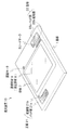
〔第1実施形態〕
図1に示すように、本発明の第1実施形態に係る発光装置10は、矩形平板状の基板1の上面の中央部に矩形の環(四角環)状の枠体7が設けられ、枠体7の内側に透明部材(透光部材)9が、その下に封止部材8が、それぞれ透光性樹脂で形成されている。さらに発光装置10は、封止部材8に被覆されて搭載された発光素子4(図1不図示)により、枠体7の内側を照射領域として光を上方へ照射する。発光装置10は、基板1の上面の枠体7の外側に、発光素子4の駆動電圧を外部から印加するための一対のパッド電極(アウターリード)として、正極21および負極22の各パッド部21c,22cが金属膜で形成されている。発光装置10においては、基板1の上面に、カソードマークおよび認識マークが、パッド部21c,22cと同様に金属膜で形成されている。カソードマークは「−」形状で、発光装置10の使用時にパッド部21c,22cを識別するために、負極22のパッド部22c近傍に設けられている。認識マークは、発光装置10の製造において、基板1に発光素子4を実装する際の、位置を認識するための目印である。カソードマークおよび認識マークは、発光装置10の仕様によって位置および形状が設計され、あるいはなくてもよく、例えばカソードマークに代えてアノードマークが正極21のパッド部21c近傍に設けられていたり(図5に示す第2実施形態参照)、アノードマークとカソードマークの両方が設けられてもよい。
[First Embodiment]
As shown in FIG. 1, the light emitting device 10 according to the first embodiment of the present invention is provided with a rectangular ring (square ring) -like frame body 7 at the center of the upper surface of a rectangular flat substrate 1. A transparent member (translucent member) 9 is formed inside the body 7, and a sealing member 8 is formed below the translucent resin. Further, the light emitting device 10 irradiates light upward using the light emitting element 4 (not shown in FIG. 1) mounted and covered with the sealing member 8 as an irradiation region. The light emitting device 10 includes a
発光装置10の、枠体7および透明部材9に被覆された部分について、図2および図3を参照して説明する。図2では、横方向に平面視長方形の基板1の長辺方向を示し、また、枠体7は輪郭線のみを二点鎖線で表し、表層の枠体7の内側(照射領域全体)に形成される封止部材8(81,82)および透明部材9(図3参照)は省略する。
A portion of the light emitting device 10 covered with the frame body 7 and the
発光装置10は、基板1上の枠体7の内側を実装領域1a(図2において右下1/4領域にのみ破線で表す)としてこの実装領域1aに発光素子4,4,…を配列して備え、実装領域1aの周囲の枠体7に被覆される領域に、正極21および負極22における発光素子4を電気的に接続するための部分であるインナーリード部(リード電極)21a,22aを備える。発光装置10は、パッド部21c,22cにて駆動電圧を印加されることにより発光素子4が発光して、封止部材8(81,82)および透明部材9を透過して枠体7の内側(図2に示す内側の輪郭線内)を照射領域として上方に光を照射する。したがって、本実施形態に係る発光装置10は、照射領域の全体の平面視形状が図2において縦に長い長方形(角丸長方形)になる。また、発光装置10は、インナーリード部21a,22aに電気的に接続された保護素子5をさらに備える。発光素子4および保護素子5は、後記するように、ボンディングワイヤ(ワイヤ)Wにてインナーリード部21a,22aに電気的に接続される。
The light emitting device 10 arranges the
発光装置10は、基板1上の照射領域にすなわち枠体7の内側に、枠体7と同じく四角環形状の透光壁(壁体)6をさらに備え、これにより照射領域が中央の第1照射領域11とその外側の第2照射領域12とに区画される。この透光壁6は、平面視において図2に示すように、配列された発光素子4,4,…に重なって設けられ、言い換えると、発光素子4,4,…は、透光壁6の配置に関わらず等間隔に配列される。なお、図2において、透光壁6は、枠体7と同様に輪郭線のみを2点鎖線(太線)で表す。このような透光壁6に重なった発光素子4は、図3に示すように、重なった領域である一部または全体がワイヤWも含めて透光壁6に埋設される。発光装置10は、発光素子4およびワイヤWを封止部材8または透光壁6に埋設することにより、そして、保護素子5、ワイヤW、およびワイヤWが接続される領域であるインナーリード部21a,22aを、枠体7に埋設することにより、塵芥、水分、外力等から保護する。以下、発光装置10を構成する要素について、詳細に説明する。
The light emitting device 10 further includes a rectangular ring-shaped translucent wall (wall body) 6 in the irradiation area on the substrate 1, that is, inside the frame body 7. It is divided into an
(基板)
基板1は、発光装置10の基材であり、発光素子4等を配置する支持体であって、図1に示すように矩形平板状に形成されている。基板1は、一般的な半導体素子のCOBパッケージ用の基板と同様に、ある程度の強度を有する絶縁性材料で形成されたものが好ましく、また、発光素子4の発光した光や外光の透過し難い光透過率の低い材料で形成されたものが好ましい。具体的には、セラミックス(Al2O3,AlN等)、あるいはフェノール樹脂、エポキシ樹脂、ポリイミド樹脂、BTレジン(bismaleimide triazine resin)、ポリフタルアミド(PPA)等の樹脂が挙げられる。これらの材料は、公知の方法で平板状に形成される。なお、基板1の形状および大きさは限定されず、製品としてユーザに提供する発光装置の形態や用途に応じて、適宜設計される。
(substrate)
The substrate 1 is a base material of the light emitting device 10 and is a support body on which the
図2に示すように、基板1(図2の全体)は、発光装置10において照射領域とする領域(枠体7の内側の輪郭線内)に、それより一回り小さいまたは略一致する平面視形状の実装領域1aが区画される。実装領域1aは、発光素子4を配置するための領域であり、発光装置10における照射領域の位置および形状に基づき設計される。基板1の上面には、前記した正極21および負極22(適宜まとめて導電層2と称する)やカソードマーク等の他に、発光素子4のそれぞれが載置される位置に、発光素子4の平面視形状よりも一回り大きい形状の反射層3,3,…が金属膜で形成されている。
As shown in FIG. 2, the substrate 1 (the whole of FIG. 2) is a plan view that is slightly smaller than or substantially coincides with a region (inside the outline inside the frame body 7) that is an irradiation region in the light emitting device 10. A shaped mounting area 1a is defined. The mounting area 1 a is an area for arranging the
(導電層)
正極21および負極22は、一対の電極として、基板1の上面に、実装領域1aを挟んで対向するように互いに離間した2つの金属膜として形成されている。正極21および負極22はそれぞれ、外部から発光素子4の駆動電圧を印加するためのパッド部21c,22c、発光素子4のパッド電極を電気的に接続するためのインナーリード部21a,22a、およびパッド部21c(22c)とインナーリード部21a(22a)を接続する配線部21b,22bからなる。パッド部21c,22cの形状および大きさならびに基板1における位置は、発光装置10において(封止後に)露出して、外部から電気的に接続可能であれば特に限定されず、発光装置10の形態や用途に応じて適宜設計される。インナーリード部21a,22aは、発光素子4,4,…のうちの配列の端に配置された発光素子4をワイヤボンディングにて接続可能なように、実装領域1aの周囲に実装領域1aから所定の間隔を空けてカギ型に形成される。
(Conductive layer)
The positive electrode 21 and the negative electrode 22 are formed as a pair of electrodes on the upper surface of the substrate 1 as two metal films separated from each other so as to face each other with the mounting region 1a interposed therebetween. The positive electrode 21 and the negative electrode 22 are
導電層2(正極21および負極22)は、一般的な半導体素子のCOBパッケージ用の基板上へリード電極のパターンに形成される金属膜を適用することができ、Au,Cu,Al等が挙げられ、Au膜が特に好ましい。後記するように、ワイヤWには金(Au)ワイヤが適用されることが多く、正極21および負極22のインナーリード部21a,22aがワイヤWと同じ材料のAu膜であれば、強固に接合し易い。あるいはCu膜等にAu膜を積層してもよく、導電層2は、異なる金属膜を2層以上積層して形成されてもよい。導電層2とする金属膜は、無電解めっきまたは電解めっきで基板1表面に形成することが好ましく、また同時にアノードマーク等を形成することができる。導電層2の厚さは特に限定されず、ワイヤボンディングの条件やリード電極としての抵抗等に応じて適宜設計される。
For the conductive layer 2 (the positive electrode 21 and the negative electrode 22), a metal film formed in a pattern of a lead electrode on a substrate for a COB package of a general semiconductor element can be applied, and examples thereof include Au, Cu, and Al. An Au film is particularly preferable. As will be described later, gold (Au) wire is often applied to the wire W, and if the
(反射層)
反射層3は、発光装置10の発光効率を向上させるために、発光素子4から下方へ出射した光を反射して発光装置10から上方へ照射させる反射膜である。さらに、本実施形態に係る発光装置10においては、両面電極構造の発光素子4(発光素子41)が搭載されるため、下面側の電極が電気的に反射層3に接続される。反射層3は、基板1の実装領域1aの発光素子4のそれぞれが載置される位置に、発光素子4の平面視形状よりも一回り大きく、かつ互いに短絡しないように反射層3,3間を空けて形成される。反射層3は、光反射率の高い金属膜であれば特に材料は限定されないが、Ag,Auが好ましく、可視光に対する反射率が高いAgが特に好ましい。AuはAgよりも光を吸収し易いが、例えば導電層2と共にAuめっき膜で反射層3を形成した後、Auめっき膜表面にTiO2膜をさらに形成することで、光反射率を高くすることができる。反射層3は、導電層2と同様に無電解めっきまたは電解めっきで基板1表面に形成することが好ましく、また反射層3の厚さは特に限定されないので、例えば導電層2と同じ厚さとして、基板1表面に同時に形成してもよい。あるいは、導電層2はAuめっき膜、反射層3はAgめっき膜として、別工程にてめっきを行ってもよい。
(Reflective layer)
The reflective layer 3 is a reflective film that reflects light emitted downward from the
(発光素子)
発光素子4は、電圧を印加することで自ら発光する半導体素子であり、窒化物半導体等から構成される公知の半導体発光素子を適用でき、面状発光装置の光源としては広い面積に光を出射する発光ダイオード(LED)が好ましい。発光素子4は、所望の発光色を得るために任意の波長のものを選択すればよい。具体的には、青色の光(波長430nm〜490nm)や緑色の光(波長490nm〜570nm)を発光する発光ダイオードとしては、InXAlYGa1-X-YN(0≦X、0≦Y、X+Y≦1)で表される窒化物系半導体を、赤色の光(波長620nm〜750nm)を発光する発光ダイオードとしては、GaAlAs,AlInGaP等で表されるヒ素系化合物やリン系化合物の半導体をそれぞれ適用することができ、さらに混晶比により発光色を変化させた発光ダイオードとなる。発光装置10から照射される光を赤色とする場合はGaAlAs等を適用すればよく、それ以外の色とする場合は、窒化物系半導体を適用し、さらに必要に応じて後記するように封止部材81,82に蛍光体を含有させる。本実施形態に係る発光装置10には、発光色の異なる2種類の発光ダイオードである発光素子41,42を搭載し、これらを適宜まとめて発光素子4と表す。
(Light emitting element)
The light-emitting
本実施形態に係る発光装置10においては、図2に示すように、発光素子4(41,42)は平面視長方形であり、基板1の実装領域1aを埋めるように、一定間隔で配列され、当該配列された発光素子4,4,…が一体となって発光装置10の照射領域から面状の光を照射する。このように発光素子4が一定間隔で配列されることで、発光装置10から照射される光は面内で一様の輝度を示す。本実施形態においては、発光素子4,4,…は、長手方向を図2における横方向に向きを揃えて、マトリクス状に6個×10列の合計60個を配列して備えられ、そのうち、第1照射領域11には4個×6列の24個の発光素子41が、第2照射領域12には36個の発光素子42が、それぞれ搭載される。
In the light emitting device 10 according to the present embodiment, as shown in FIG. 2, the light emitting elements 4 (41, 42) are rectangular in plan view, and are arranged at regular intervals so as to fill the mounting region 1 a of the substrate 1. The arranged
また、本実施形態に係る発光装置10に搭載された発光素子41,42は、フェイスアップ(FU)実装に対応し、図3に示すように、発光素子41は両面電極構造で、一対のパッド電極のp電極が上面に、n電極が下面に形成され、発光素子42は一対のパッド電極が共に上面に形成されている。したがって、発光素子41は、基板1の実装領域1aに配列される際に、反射層3表面に、はんだや導体ペースト等の公知の導電性の接合部材により底面を接合されると同時にn電極が電気的に接続される。同様に発光素子42も、底面を反射層3表面に接合されるが、樹脂等の非導電性の接合部材を用いてもよい。そして、発光素子41については、p電極は直接にワイヤボンディングにてワイヤWと接続され、n電極は反射層3がワイヤWと接続される。一方、発光素子42は、p電極およびn電極が共にワイヤWと接続される。
Further, the
さらに発光素子41,42はp電極を形成された側を図2および図3における左に向きを揃えて配列され、それぞれの発光素子4(41,42)は、正極21のインナーリード部21aの近傍の配列の端に配置した発光素子4(42)から負極22のインナーリード部22a近傍の配列の端に配置した発光素子4(42)までを、隣り合う発光素子4を1個以上経由して、あるいは経由せずに2個を、直列にワイヤWで接続されることにより、インナーリード部21a,22aに電気的に接続される。このように接続されることで、実装領域1aに2次元に配列された発光素子4,4,…のすべてについて、実装領域1aの外側のインナーリード部21a,22aから電圧を印加することができる。
Further, the
ここで、発光装置10において、直列に接続される発光素子4の組は、その発光素子4の個数が同数に統一されていることが望ましい。発光素子4,4,…は、組単位で並列にインナーリード部21a,22aに接続されて、共通の電圧を印加されるので、組毎に発光素子4の個数が異なると抵抗が異なって、組によって発光素子4の1個あたりに印加される電圧に差が生じて発光する光の光量が一様にならず、照射領域に輝度の面内ばらつきが生じる。さらに本実施形態に係る発光装置10のように、順方向降下電圧Vfの異なる2種類以上の発光ダイオード(発光素子41,42)を搭載する場合は、発光素子41,42それぞれの個数を統一する。具体的には、図2に示すように、6個の発光素子41と9個の発光素子42の計15個で一組として直列に接続し、4組を並列に接続する。このように、発光素子4(41,42)の搭載個数や配列に応じて接続仕様を設計する。あるいは、すべての発光素子4を1個ずつ並列に接続してもよく、例えば各発光素子4のp電極同士、n電極同士をそれぞれワイヤで接続してインナーリード部21a,22aまで接続すればよい(図示省略)。
Here, in the light emitting device 10, it is desirable that the number of the
(保護素子)
保護素子5は、ツェナーダイオードやコンデンサ等であり、過電圧印加による発光素子4の破壊を防止するために搭載される。保護素子5は、発光素子4から出射する光を遮らないように照射領域の外に配置されることが好ましく、したがって、枠体7に埋設されていることが好ましい。本実施形態に係る発光装置10においては、保護素子5は底面に図示しないアノード電極を備えてインナーリード部21a表面にはんだや導体ペースト等にて接続され、上面に備えたカソード電極がインナーリード部22aにワイヤボンディングにて接続される。
(Protective element)
The protection element 5 is a Zener diode, a capacitor, or the like, and is mounted in order to prevent the
(ワイヤ)
ワイヤWは、発光素子4(41,42)や保護素子5のような電子部品を正極21および負極22のインナーリード部21a,22aへ電気的に接続するための導電性の配線である。ワイヤWは、ワイヤボンディングにて一般的に使用されるワイヤであり、材料としては、Au,Cu,Pt,Alまたはそれらの合金が挙げられる。特に熱伝導率等に優れ、また発光素子4のパッド電極材料に一般に適用されるAuが好ましい。また、ワイヤWの径は特に限定されず、ワイヤWの材料、抵抗、ワイヤボンディングの条件、発光素子4や保護素子5の仕様等に応じて適宜選択される。
(Wire)
The wire W is a conductive wiring for electrically connecting electronic components such as the light emitting element 4 (41, 42) and the protection element 5 to the
(枠体、透光壁)
枠体7は基板1上に発光装置10の照射領域全体を区画し、この照射領域を透光壁6がさらに2つの照射領域11,12に区画する。透光壁6および枠体7は、後記するように、透光性樹脂材料を当該透光壁6、枠体7の内側、透光壁6と枠体7との間にそれぞれ充填して封止部材81,82および透明部材9を形成するための堰である。
(Frame, translucent wall)
The frame body 7 divides the entire irradiation area of the light emitting device 10 on the substrate 1, and the
枠体7は、封止部材81,82や透光壁6と共にワイヤW等を封止(埋設)してこれを保護する。したがって、枠体7は、図2に示すように、実装領域1aを囲うようにインナーリード部21a,22aを被覆する領域に矩形(縦に長い長方形)の環状に形成され、これに伴い、これらに接続するワイヤW、ならびにインナーリード部21a上の保護素子5を埋設する。さらに枠体7は、その内壁面で発光素子4から側方へ出射した光を上方へ反射させて発光装置10の発光効率を向上させるための反射板である。あるいは、枠体7は、透光壁6と同様に光を透過させる材料で形成されて、発光装置10の照射領域から側方へも光が照射される構成としてもよい。
The frame body 7 seals (embeds) the wires W and the like together with the sealing
枠体7は絶縁体であり、基板1と同様に、ある程度の強度を有し、発光素子4の発光した光や外光の透過し難い光透過率の低い材料で形成されることが好ましい。さらに、枠体7は、先にワイヤボンディングで設けられたワイヤWをできるだけ変形させないように埋設するために、基板1上へ液状やペースト状で成形してそのまま凝固させて形成できる材料を適用する。詳しくは後記製造方法にて説明するが、堰として十分な高さに形成するために、ペースト状すなわち高粘度の液状の材料が好ましい。このような材料として熱硬化性樹脂や熱可塑性樹脂が挙げられ、具体的には、フェノール樹脂、エポキシ樹脂、BTレジン、PPA、シリコーン樹脂等が挙げられる。また、枠体7は、反射率を高くするために白色であることが好ましい。さらに枠体7は、反射率をいっそう高くするために、前記樹脂材料に、発光素子4が発光した光を吸収し難く、かつ母材である当該樹脂に対して屈折率差の大きい反射材料(例えばTiO2,Al2O3,ZrO2,MgO等)の粉末を、予め分散させて形成してもよい。
The frame body 7 is an insulator and is preferably formed of a material having a certain level of strength and having a low light transmittance through which light emitted from the
枠体7は、基板1からの高さを特に規定しないが、図3に示すように、透光壁6およびその内外に充填されて形成される封止部材81,82のさらに上の照射領域全体に、当該枠体7の内側に透明部材9を充填して形成するために、透光壁6よりも高いことが好ましい。また、枠体7は、発光素子4から側方へ出射して照射領域の外側へ向かう光をそのまま発光装置10の外に出射させないように、反射面を形成する高さにする。また、枠体7は、平面視における幅(壁の厚み)を特に規定せず、インナーリード部21a,22aを被覆し、かつ所望の高さに形成することができる幅とすればよい。
The frame body 7 does not particularly define the height from the substrate 1, but as shown in FIG. 3, as shown in FIG. 3, the irradiation region further above the
透光壁6は、第1封止部材81と第2封止部材82を分離させて形成するための堰であり、これにより発光装置10の照射領域を第1照射領域11と第2照射領域12とに区画する。さらに透光壁6は、自身が照射領域11,12の一方の一部を構成するために、封止部材81,82と同様に光を透過する材料で形成される。詳しくは、本実施形態において、透光壁6は閉じた環状であり、当該透光壁6およびその内側で構成される第1照射領域11と外側で構成される第2照射領域12とに区画する。すなわち、図2に示す透光壁6の外側の輪郭線が、第1照射領域11と第2照射領域12との境界線となる。透光壁6が設けられることにより、封止部材81,82が、透光壁6の内側と外側それぞれに液状の樹脂材料を充填して形成されるので、硬化前においてもこれらの樹脂材料が透光壁6に隔てられて互いに混入することがなく、一方のみに、または互いに異なる蛍光体を含有させることができる。
The
さらに透光壁6は、光を透過する材料で形成されるため、発光素子4を被覆して形成されても、発光素子4が発光した光は当該透光壁6の外へ取り出される(図4(a)参照)ので、透光壁6は、発光素子4の配列に合わせることなく任意の平面視形状に形成することができる。言い換えると、発光装置10は、基板1上(実装領域1a)の透光壁6の形成される位置を避けて発光素子4を配列する必要がなく、照射領域11,12間の境界等においても一定間隔で配列することができるため、照射領域全体における光量のムラが低減される。さらに、発光装置10の製造において、基板1への発光素子4の搭載の作業性が低下せず、また発光素子4,4間のワイヤWの接続(ワイヤボンディング)が容易である。ただし、本実施形態においては、照射領域11,12は、それぞれ異なる発光色の発光素子41,42が搭載されるため、境界線が発光素子41,42の載置された間となるように区画されることが好ましい。したがって、図2に示すように、透光壁6は、少なくとも外側の輪郭線が発光素子4(41,42)の配列に沿うように、枠体7と同様に四角環形状に形成されて、中心が照射領域全体の中心と略一致する縦に長い長方形の第1照射領域11とこれを囲む四角環形状の第2照射領域12とに区画する。
Further, since the
透光壁6は、光を透過する絶縁体であって、先に基板1上に搭載された発光素子4およびワイヤボンディングで設けられたワイヤWを埋設(封止)する。そのため、透光壁6は、封止部材81,82と同様に、シリコーン樹脂、エポキシ樹脂、ユリア樹脂等の透光性樹脂材料を適用することができ、発光装置10の形態や用途に応じて選択され、例えば、発光素子4として高出力の発光ダイオードを搭載する場合には、特に耐熱性に優れたシリコーン樹脂が好ましい。そして、枠体7と同様に、粘度を調整してペースト状とした前記樹脂材料を基板1上に成形してそのまま凝固させて形成される。詳しくは後記製造方法にて説明する。
The
さらに、透光壁6は、当該透光壁6を含む第1照射領域11から、配列する発光素子4(41)が発光する光を波長変換させて照射する場合は、第1封止部材81と同様に、蛍光体を前記樹脂材料に添加する(第3実施形態参照)。ただし、透光壁6は、前記した通り形成時において高粘度の樹脂材料であるので、添加、混合した蛍光体が均一に分散した状態をある程度保持して硬化する。そのため、蛍光体が沈殿し易く発光素子4近傍に偏って分布する封止部材81,82と比較して、光の取出し効率が低くなり易い。また、同じ第1照射領域11において、透光壁6と第1照射領域11とで蛍光体の分布状態が異なるので、それぞれから照射する光の色を一致させることが困難である。したがって、照射領域11,12の一方のみにおいて蛍光体で波長変換した光を照射する場合は、蛍光体を含まない方に透光壁6を含む構成とすることが好ましい。このように透光壁6(第1照射領域11)は、蛍光体を含有しない場合には、第2照射領域12から照射される光と光量を均衡化するべく、第1封止部材81と共に光拡散剤を添加されてもよい。
Further, when the
透光壁6は、基板1からの高さを特に規定しないが、図3に示すように、内側および外側の枠体7との間に充填されて形成される封止部材81,82が発光素子4およびワイヤWを完全に埋設して露出させない高さとなるようにする。一方、透光壁6は、後記するように上に透明部材9が形成されるため、枠体7よりも低いことが好ましい。また、透光壁6は、平面視における幅(壁の厚み)を特に規定せず、所望の高さに形成することができる幅とすればよい。ただし、透光壁6の幅が太過ぎると、第1封止部材81を充填する領域が小さくなる。
The
(封止部材)
本発明に係る発光装置10は、発光素子4およびワイヤWを封止(埋設)してこれらを保護し、かつ発光素子4が発光した光を透過させて外部へ取り出すための封止部材8として、図2に示すように、平面視で2つに区画された領域(照射領域11,12)のそれぞれに第1封止部材81および第2封止部材82を備える。詳しくは、第1封止部材81は透光壁6の内側に、第2封止部材82は透光壁6の外側であって枠体7との間に、それぞれ基板1上に液状の樹脂材料を充填して、前記したように発光素子4およびワイヤWを完全に埋設して露出させない高さに形成される。さらに、第1封止部材81および第2封止部材82の少なくとも一方は、蛍光物質(蛍光体)を含有して光が透過する際にその波長を変換する。
(Sealing member)
The light emitting device 10 according to the present invention serves as a sealing member 8 that seals (embeds) the
封止部材81,82は、発光ダイオード等を搭載した一般的な発光装置の封止に用いられる透光性樹脂材料を適用することができ、具体的には、シリコーン樹脂、エポキシ樹脂、ユリア樹脂等が挙げられる。また、封止部材81,82は、先に基板1上に形成された透光壁6、枠体7が堰になるので、比較的低粘度の液状の樹脂材料で形成することができ、本実施形態に係る発光装置10のように広い領域(照射領域11,12)を封止するために好適である。また、封止部材81,82は、それぞれの樹脂材料が透光壁6に隔てられて互いに混入することがないので、蛍光体を一方のみにまたは互いに異なる種類を含有させることができる。さらに、このような低粘度の樹脂材料に蛍光体を混合した場合、硬化するまでに蛍光体が沈殿し易いので、図4(a)に示す第2封止部材82のように、基板1上に載置された発光素子4の表面(上面および側面)近傍に偏って蛍光体FLが分布して、発光素子4が発光した光が好適に波長変換される。また、これらの樹脂材料に、発光装置10の目的や用途に応じて前記蛍光体の他に、着色剤、光拡散剤、フィラー等を含有させてもよい。以下、封止部材81,82、さらに透光壁6に含有させる蛍光体について説明する。
As the sealing
蛍光体は、発光素子4が発光した光の少なくとも一部を吸収して異なる波長の光に変換する波長変換部材である。蛍光体は公知の材料を適用すればよく、例えばY(イットリウム)、Al(アルミニウム)、およびGa(ガーネット)を混合してCe等で賦活されたYAG系蛍光体や、Eu,Ce等のランタノイド系元素で主に賦活された、窒化物系蛍光体、酸窒化物系蛍光体等を用いることができる。これらの材料から、後記するように発光素子4の発光色と組み合わせて、第1照射領域11、第2照射領域12から照射する光が所望の色となるように選択する。例えば、緑色や黄色を発光するYAG系蛍光体やクロロシリケート蛍光体、赤色を発光する(Sr,Ca)AlSiN3:Eu等のSCASN系蛍光体、CaAlSiN3:Eu等のCASN系蛍光体が挙げられ、また2種類以上の蛍光体を混合して用いてもよい。
The phosphor is a wavelength conversion member that absorbs at least part of the light emitted from the
(透明部材)
発光装置10においては、その照射領域の全体を被覆する透明部材9を備えることが好ましい。透明部材9は、図3に示すように、透光壁6および封止部材81,82により形成された表面の凹凸を均すようにこれらの上に形成されて発光装置10の外観を整え、また、透光壁6および封止部材81,82のそれぞれから照射した光を一体として取り出すことができる。透明部材9は、封止部材81,82と同様に、透光性樹脂材料を枠体7の内側に充填して形成される。透光壁6の表面形状は限定されず、例えば平坦であっても凸レンズ状(図5参照)であってもよく、製品としてユーザに提供する発光装置10の形態や用途に応じて適宜設計される。
(Transparent material)
The light emitting device 10 preferably includes a
(発光装置の製造方法)
次に、本発明の実施形態に係る発光装置の製造方法の一例を説明する。発光装置10は、一般的な半導体素子のCOBパッケージや従来の発光装置と同様の方法で製造できる。また、基板1が面方向に発光装置10の複数台分が連結した状態で製造されてもよく、この場合は、最後(透明部材9を形成した後)に、1台ずつに基板1を切断、分離して完成となる。
(Method for manufacturing light emitting device)
Next, an example of a method for manufacturing a light emitting device according to an embodiment of the present invention will be described. The light emitting device 10 can be manufactured by a method similar to that of a general semiconductor element COB package or a conventional light emitting device. Further, the substrate 1 may be manufactured in a state where a plurality of light emitting devices 10 are connected in the surface direction. In this case, the substrate 1 is cut one by one at the end (after the
まず、基板1の表面(上面)に、無電解めっきで金属膜を所定の形状にパターニングした導電層2および反射層3を形成する。このとき、同時にまたは前後してカソードマークおよび認識マーク(図1参照)を形成することができる。 First, the conductive layer 2 and the reflective layer 3 are formed on the surface (upper surface) of the substrate 1 by patterning a metal film into a predetermined shape by electroless plating. At this time, the cathode mark and the recognition mark (see FIG. 1) can be formed simultaneously or before and after.
次に、基板1上の実装領域1aに所定の間隔で形成された反射層3に、発光素子4(41,42)を搭載、配列する。このとき、発光素子4の底面を接合部材で反射層3に接合する。また、保護素子5をインナーリード部21a上の所定位置に搭載する。接合部材によっては、すべての発光素子4および保護素子5を配列した後、基板1を加熱して接合部材を硬化する、あるいは溶融して接着固定する。なお、発光素子41,42および保護素子5の搭載順序は限定されない。そして、ワイヤボンディングにより、搭載した発光素子4および保護素子5のそれぞれのパッド電極または反射層3にワイヤWを接続し、インナーリード部21a,22aへ電気的に接続する。
Next, the light emitting elements 4 (41, 42) are mounted and arranged on the reflective layer 3 formed at a predetermined interval in the mounting region 1a on the substrate 1. At this time, the bottom surface of the
次に、透光壁6および枠体7を形成する。詳しくは、透光壁6、枠体7それぞれの平面視形状に合わせた環形状の吐出口(ノズル)を備えた樹脂吐出装置にて、ペースト状の樹脂材料を基板1上の枠体7の形成位置に吐出し、熱処理等の樹脂材料に対応した処理により硬化または凝固させる。あるいは、透光壁6、枠体7の幅(環の太さ)に合わせた口径の吐出口で、基板1を載置した台を透光壁6、枠体7の平面視形状に合わせて長方形を描くように水平に移動させながら樹脂材料を吐出して、透光壁6および枠体7を形成することもできる。なお、透光壁6および枠体7は樹脂材料を同時に吐出してもよく、また同時に熱処理等にて硬化させてもよく、あるいはいずれか一方を硬化させてから他方を形成してもよい。
Next, the
次に、透光壁6の内側、および外側であって枠体7との間のそれぞれに、所望の蛍光体を含有させた透光性樹脂材料を充填して、必要に応じて熱処理や光照射等の処理により硬化させて第1封止部材81および第2封止部材82を形成する。封止部材81,82は、それぞれの透光性樹脂材料を同時に充填してもよく、また同時に硬化させてもよく、あるいはいずれか一方を硬化させてから他方を充填してもよい。また、透光壁6のみを形成してその内側に第1封止部材81を形成した後に、枠体7を形成して第2封止部材82を形成することもできる。さらに、例えば第1封止部材81が蛍光体等を含有しない透明な透光性樹脂材料で形成される場合は、第2封止部材82のみを形成した後に、次の透明部材9と一体に第1封止部材81を形成することもできる。
Next, a translucent resin material containing a desired phosphor is filled in the inside and outside of the
最後に、枠体7の内側に透明な透光性樹脂材料を充填し、封止部材81,82と同様に硬化して透明部材9を形成することにより、発光装置10が完成する。透明部材9の表面形状を凸レンズ状に形成する場合は、ある程度高粘度の樹脂材料を適用すればよい。
Finally, a transparent translucent resin material is filled inside the frame body 7 and cured in the same manner as the sealing
(発光装置の設計)
面状発光装置において、2以上に区画された照射領域のそれぞれから異なる色の光を照射して、全体で混色された一体の光とするためには、照射領域中心から外周に向けて色を変化させることが好ましい。発光素子として発光ダイオードを配列して搭載した発光装置においては、発光素子のそれぞれが光を全方位に放射することから、照射領域の境界近傍で混色される光が均一となる。以下、本発明の第1実施形態に係る発光装置の設計の一例を説明する。
(Light emitting device design)
In the planar light emitting device, in order to irradiate light of different colors from each of the irradiation areas divided into two or more, and to obtain integrated light that is mixed as a whole, the color is changed from the center of the irradiation area toward the outer periphery. It is preferable to change. In a light-emitting device in which light-emitting diodes are arranged and mounted as light-emitting elements, each of the light-emitting elements emits light in all directions, so that the light mixed in the vicinity of the boundary of the irradiation region becomes uniform. Hereinafter, an example of the design of the light emitting device according to the first embodiment of the present invention will be described.
本実施形態に係る発光装置10は、図2に示すように、照射領域の全体と同じく縦に長い長方形で中心が略一致する第1照射領域11と、これを囲む第2照射領域12とが区画され、それぞれ異なる色の光を照射して全体として自然光に近い白色光となるように設計される。ここでは、第1照射領域11において、発光素子41を赤色LEDとし、波長変換をせずに赤色の光を照射する。一方、第2照射領域12において、発光素子42を青色LEDとし、黄色蛍光体により白色の光を照射する。このような構成により、第2照射領域12からの青色みがかった白色光に第1照射領域11からの赤色の光が混色して白熱電球光に近い光(色温度2700〜4000Kの光)が照射される。さらに、照射領域の最外周の第2照射領域12から当該照射領域の全体で表そうとする白色光により近い光を照射することにより、発光装置10の照射面に正対していない方向から見ても比較的均一な色の光が照射される。
As shown in FIG. 2, the light emitting device 10 according to the present embodiment includes a
発光装置10においては、透光壁6は蛍光体を要しない第1照射領域11に設けられることが好ましい。前記した通り、製造時において、高粘度の樹脂材料で形成する透光壁6では蛍光体が沈殿し難く、蛍光体による波長変換効率を封止部材81,82と同等にすることが困難であるからである。なお、図2に示すように、透光壁6は、8個の発光素子41について一部が埋設されるように形成されているが、幅を太く広げて、発光素子41の全体が埋設されてもよい(第4実施形態参照)。また、発光素子41,42の出力の違い等にもよるが、第1照射領域11においては波長変換に伴う光の吸収がないので、発光素子41,42の1個あたりの光量が第2照射領域12よりも多い。そのため、第1照射領域11の方を面積および発光素子41の搭載個数をより少なくし、さらに必要に応じて第1封止樹脂81および透光壁6に光拡散剤を含有させて、第2照射領域12との光量の均衡をとることが好ましい。
In the light emitting device 10, it is preferable that the
(発光装置の動作)
このように設計された第1実施形態に係る発光装置の動作(光の照射)について、図4(a)を参照して説明する。図4(a)では、発光素子4(41,42)のパッド電極、ワイヤW、および反射層3を省略する。
(Operation of light emitting device)
The operation (light irradiation) of the light emitting device according to the first embodiment designed as described above will be described with reference to FIG. In FIG. 4A, the pad electrode, the wire W, and the reflective layer 3 of the light emitting element 4 (41, 42) are omitted.
第1実施形態に係る発光装置10においては、第2封止部材82中に蛍光体FLが沈殿して発光素子4(42)表面近傍に偏って分布している。そのため、発光素子42が発光した光は、蛍光体FLにより効率よく波長変換されて第2封止部材82、さらに透明部材9を透過して発光装置10の外へ照射される。ここで、発光素子4(41,42)は、当該発光素子4の発光層(活性層)から全方位に光を放射するため、上方だけでなく、側方や下方へも光が出射される。そのため、発光素子42から側方へ出射したり下方へ出射して反射層3で反射した光の一部(例えば光線L2)は、第2封止部材82から第1照射領域11の透光壁6に進入し、あるいはさらに第1封止部材81に進入する。これら透光壁6等は蛍光体を含有しないため、発光素子42から出射して第2封止部材82において波長変換された光は、透光壁6や第1封止部材81により波長変換されたり吸収されることなく、透明部材9を透過して第1照射領域11から発光装置10の外へ照射される。
In the light emitting device 10 according to the first embodiment, the phosphor FL is precipitated in the second sealing
一方、第1照射領域11の第1封止部材81や透光壁6に埋設された発光素子4(41)が発光した光の一部(例えば光線L1,L3)は、第2封止部材82に進入する。しかし、第2封止部材82において蛍光体FLは底(基板1上および発光素子42上)に沈殿して存在するので、発光素子41からの光は第2封止部材82を透過する際に吸収等されることなく、さらに透明部材9を透過して第2照射領域12から発光装置10の外へ照射される。
On the other hand, a part of light (for example, light rays L 1 and L 3 ) emitted from the first sealing
このように、照射領域11,12間が遮光されないため、照射領域11,12それぞれに載置された発光素子41,42が発光した光、あるいはさらに波長変換された光は、照射領域11,12境界近傍で混色しながら発光装置10の外へ照射される。したがって、発光装置10は、照射領域全体で一体に近い光を取り出すことができる。
In this way, since the
以上のように、第1実施形態に係る発光装置は、照射領域を2以上に区画してもその境界近傍を含めて発光素子を均等に配列することができるので輝度が低下せず、さらに隣り合う照射領域のそれぞれで、搭載した発光素子の発光色および蛍光体の有無の両方を切り替えることができるので、配色の選択性が広く、演色性を向上させることができる。 As described above, in the light emitting device according to the first embodiment, even if the irradiation area is divided into two or more, the light emitting elements can be arranged evenly including the vicinity of the boundary. Since both the emission color of the mounted light emitting element and the presence or absence of the phosphor can be switched in each of the matching irradiation regions, the coloration selectivity is wide and the color rendering can be improved.
〔第2実施形態〕
第1実施形態に係る発光装置は、照射領域をマトリクス状の発光素子の配列に沿うように区画して、それぞれの照射領域に異なる発光色の発光素子を搭載したが、発光素子の配列に合わせることなく任意の平面視形状に区画されてもよい。以下、第2実施形態に係る発光装置について、図5および図6を参照して説明する。第1実施形態に係る発光装置10と同一の要素については同じ符号を付して説明を省略する。
[Second Embodiment]
In the light emitting device according to the first embodiment, the irradiation area is partitioned along the arrangement of the matrix light emitting elements, and the light emitting elements having different emission colors are mounted in the respective irradiation areas. It may be divided into any plan view shape without. Hereinafter, the light emitting device according to the second embodiment will be described with reference to FIGS. 5 and 6. The same elements as those of the light emitting device 10 according to the first embodiment are denoted by the same reference numerals, and description thereof is omitted.
第2実施形態に係る発光装置10Aは、図5に示すように、第1実施形態に係る発光装置10(図1参照)と同様に、矩形平板状の基板1Aの上面の中央部に環状の枠体7Aが設けられ、その内側に透明部材9Aが、その下に図示しない封止部材8(図1参照)が、それぞれ形成され、枠体7Aの内側に照射領域を構成する。本実施形態では、枠体7Aは円環形状であるので照射領域は円形になる。また、透明部材9Aは、表面形状を凸レンズ状に形成されているが、例えば平坦でもよい。また、基板1Aの上面に、カソードマークに代えてアノードマークが、さらに温度計測ポイントが金属膜で形成される。温度計測ポイントは、発光装置10Aに搭載された発光素子4の動作温度およびジャンクション温度を検査するために、当該表面で温度を計測する金属膜である。正極21Aおよび負極22Aの各パッド部21c,22c、および認識マークは、形状以外は発光装置10と同様であるので、説明を省略する。
As shown in FIG. 5, the light emitting device 10 </ b> A according to the second embodiment has an annular shape at the center of the upper surface of the rectangular plate-like substrate 1 </ b> A, similarly to the light emitting device 10 according to the first embodiment (see FIG. 1). A frame body 7A is provided, a
発光装置10Aの、枠体7A、透明部材9Aおよび封止部材8に被覆された部分について、図6を参照して説明する。図6では、縦方向に平面視長方形の基板1Aの長辺方向を示し、また、枠体7Aおよび透光壁6Aは輪郭線のみを2点鎖線で表し、枠体7Aの内側に形成される透明部材9Aおよび封止部材8(81,82)は省略する。
A portion of the light emitting device 10A covered with the frame 7A, the
発光装置10Aは、基板1A上の枠体7Aの内側の輪郭線内の、当該輪郭線よりも一回り小さい円形の実装領域1a(図6において左上1/4領域にのみ破線で表す)に、発光素子4,4,…を配列して備える。基板1A上の実装領域1aの周囲には、インナーリード部21a,22aが、円形の実装領域1aから所定の間隔を空けて半円周に沿った形状に形成される。
The light emitting device 10A has a circular mounting region 1a (indicated by a broken line only in the upper left quarter region in FIG. 6) in the inner contour line of the frame 7A on the substrate 1A that is slightly smaller than the contour line. The
さらに発光装置10Aは、基板1A上の照射領域に、すなわち枠体7Aの内側に、枠体7Aと同心円状の円環形状の透光壁(壁体)6Aをさらに備えて、中心が照射領域全体の中心と略一致する円形の第1照射領域11Aとこれを囲む円環形状の第2照射領域12Aとに区画される。本実施形態においては、第1実施形態と同様に、透光壁6Aは第1照射領域11Aの一部を構成し、透光壁6Aの外側の輪郭線が照射領域11A,12Aの境界線となる。このように、透光壁6Aは平面視で曲線状に形成されているため、以下に記載するようにマトリクス状に配列された発光素子4,4,…は、その一部が照射領域11A,12Aの境界線を跨いで載置される。
Furthermore, the light emitting device 10A further includes an annular light transmitting wall (wall body) 6A concentric with the frame body 7A in the irradiation area on the substrate 1A, that is, inside the frame body 7A. It is divided into a circular
発光装置10Aには、発光素子4として、発光色の異なる2種類の発光ダイオードである発光素子43,42が搭載される(第1実施形態と同様に、適宜まとめて発光素子4と表す)。発光素子43,42は、平面視長方形の同一形状で、第1実施形態の発光素子42(図3参照)と同様に一対のパッド電極が共に上面に形成されている。発光素子4(発光素子43,42)は、長手方向を図6における横方向に、かつp電極を左側に向きを揃えて、実装領域1aの中央に9個×8列をマトリクス状に、その上下に各3列を横方向に半ピッチずらし、計14列に配列され、さらに配列の左右両端の各3個を右に90°回転して配置される。このように配列されることで、図6における左右上下対称に、計110個の発光素子4が、均等にかつ効率的に実装領域1aに搭載される。そのうち、第1照射領域11Aには60個の発光素子43が、第2照射領域12Aには50個の発光素子42が、それぞれ搭載される。
In the light emitting device 10A,
本実施形態に係る発光装置10Aは、60個の発光素子43と50個の発光素子42の2種類の発光素子4を搭載しているため、ワイヤWにて、6個の発光素子43と5個の発光素子42の計11個で一組として直列に接続し、10組を並列に接続する。また、発光装置10Aにおいては、発光素子4(43,42)はすべて、一対のパッド電極が共に上面に形成されているので、配列の端のインナーリード部21a,22aに直接に接続した発光素子4以外の発光素子4については、隣の発光素子4のパッド電極へワイヤWを接続すればよい。したがって、ワイヤWの両端の接続位置の高低差が小さく、発光素子4,4間隔が比較的短く配列されてもワイヤボンディングが容易である。
Since the light emitting device 10A according to the present embodiment is equipped with two types of
また、本実施形態に係る発光装置10Aに搭載された発光素子4(43,42)はすべて、一対のパッド電極が共に上面に形成されているため、第1実施形態のように金属膜(反射層3)に接合する必要はなく、かつ発光素子4毎に分離した金属膜とする必要もない。発光装置10Aにおいては、反射層3Aは、基板1Aの実装領域1aの全体に、当該実装領域1aよりも一回り大きい円形で、かつ正極21Aと負極22Aとが短絡しないようにインナーリード部21a,22aから間隔を空けて形成される。なお、基板1Aが、例えばアルミナ(Al2O3)で形成されている等、表面の反射率が十分に高い場合は反射層3Aを設けなくてもよい。
In addition, since all of the light emitting elements 4 (43, 42) mounted on the light emitting device 10A according to the present embodiment have a pair of pad electrodes formed on the upper surface, the metal film (reflective) as in the first embodiment. It is not necessary to bond to the layer 3), and it is not necessary to use a metal film separated for each light emitting
(発光装置の設計および動作)
次に、本発明の第2実施形態に係る発光装置の設計の一例およびその動作(光の照射)を説明する。本実施形態に係る発光装置10Aは、第1実施形態に係る発光装置10と同様に、照射領域の全体と中心が略一致する第1照射領域11Aと、これを囲む第2照射領域12Aとが区画され、それぞれ異なる色の光を照射する。ここでは、第1照射領域11Aにおいて、発光素子43を緑色LEDとし、波長変換をせずに緑色の光を照射する。一方、第2照射領域12Aにおいて、発光素子42を青色LEDとし、赤色蛍光体により赤紫(マゼンタ)色の光を照射する。したがって、発光装置10Aにおいては、第1実施形態と同様に、透光壁6Aは蛍光体を要しない第1照射領域11Aに設けられることが好ましい。なお、当然ながら発光装置10と同じ配色としてもよい。
(Light emitting device design and operation)
Next, an example of the design of the light emitting device according to the second embodiment of the present invention and its operation (light irradiation) will be described. As with the light emitting device 10 according to the first embodiment, the light emitting device 10A according to the present embodiment includes a
図2に示す第1実施形態に係る発光装置10と異なり、本実施形態においては、発光素子4(43,42)の配列に合わせることなく照射領域11A,12Aが区画される。したがって、照射領域11A,12Aの境界線上においては、照射領域11A,12Aの一方に搭載された発光素子43または発光素子42の一部が他方へ突出する。ここでは、図6に示すように、第1照射領域11Aに搭載された発光素子43の8個について、それぞれの一部が透光壁6Aから突出して第2照射領域12Aの第2封止部材82に埋設される。このような発光素子43の第2封止部材82に埋設された部分から出射した光は、第2封止部材82に含有される赤色蛍光体によって緑色から黄色の光に変換されるため、照射領域11A,12A境界近傍から局所的に黄色の光が照射されることになる。ただし、このような光は、発光装置10Aの照射領域の全体から照射される光に対して微少であり、さらに第1実施形態にて図4(a)を参照して説明したように、照射領域11A,12Aのそれぞれから照射した光は境界近傍で混色しながら発光装置10Aの外へ照射される。したがって、かかる構成としても、発光装置10Aは、照射領域全体で一体に近い光を取り出すことができる。
Unlike the light emitting device 10 according to the first embodiment shown in FIG. 2, in the present embodiment, the
なお、発光装置10Aを、第1実施形態に係る発光装置10と同じ配色とした場合は、発光素子43は赤色LEDであるから、第2封止部材82に埋設された部分では黄色蛍光体によって吸収される。また、照射領域11A,12Aの区画を変えて、発光素子42が第1照射領域11Aへ突出する構成としてもよい。すなわち発光素子42はその一部が透光壁6Aに埋設されるので、青色の光が波長変換されることなく外部へ照射される。このように、発光素子43,42の発光色および第2封止部材82に含有された蛍光体の種類によって、照射領域12A,11Aへ突出した発光素子43または発光素子42から照射する光の色または光の有無が異なる。しかし、いずれにおいても、発光装置10Aが照射する光の全体への影響は微少であり、さらにより影響を抑えるために、発光素子43,42のいずれが照射領域11A,12A境界線上に載置されるかを選択し、あるいは発光素子43,42の照射領域12A,11Aへ突出する部分ができるだけ少なくなるように、照射領域11A,12Aを区画すればよい。
When the light emitting device 10A has the same color scheme as that of the light emitting device 10 according to the first embodiment, the light emitting element 43 is a red LED. Therefore, the portion embedded in the second sealing
以上のように、第2実施形態に係る発光装置は、均等に配列された発光素子のそれぞれの位置に関係なく任意の平面視形状に形成された透光壁によって区画された照射領域毎に、異なる色に配色された光を照射する。したがって、特に円形等の曲線からなる形状に照射領域が区画されても、発光素子を隣り合う照射領域の間で間隔を空けて配列したり、搭載個数を減らす必要がないため、照射領域全体として輝度が均一かつ照射される光量が多い発光装置となる。 As described above, the light-emitting device according to the second embodiment is provided for each irradiation region defined by the light-transmitting walls formed in an arbitrary plan view shape regardless of the positions of the light-emitting elements arranged uniformly. Irradiate light with different colors. Therefore, even if the irradiation region is partitioned into a shape made of a curve such as a circle, it is not necessary to arrange the light emitting elements at intervals between adjacent irradiation regions or to reduce the number of mounted elements. The light emitting device has a uniform luminance and a large amount of irradiated light.
〔第3実施形態〕
第1、第2実施形態に係る発光装置は、区画した照射領域のそれぞれに、発光色の異なる発光素子を搭載し、さらに隣り合う照射領域の一方のみに蛍光体を含有した封止部材を設けて波長変換された光を照射するが、照射領域の他方にも、透光壁を含めて蛍光体にて波長変換された光を照射することもできる。以下、図5に示す第2実施形態に係る発光装置と同じ外観の発光装置について、透光壁に蛍光体を含有させた態様について、図7および図4(b)、(c)を参照して説明する。第1、第2実施形態と同一の要素については同じ符号を付して説明を省略する。
[Third Embodiment]
In the light emitting device according to the first and second embodiments, a light emitting element having a different emission color is mounted in each of the divided irradiation areas, and a sealing member containing a phosphor is provided only in one of the adjacent irradiation areas. The wavelength-converted light is irradiated, but the other of the irradiation regions can be irradiated with the light whose wavelength has been converted by the phosphor including the translucent wall. Hereinafter, with respect to the light emitting device having the same appearance as the light emitting device according to the second embodiment shown in FIG. 5, refer to FIG. 7, FIG. 4B, and FIG. I will explain. The same elements as those in the first and second embodiments are denoted by the same reference numerals and description thereof is omitted.
第3実施形態に係る発光装置10Bは、透光壁6B、ならびに照射領域11B,12Bの区画および第1封止部材81Aの構成、さらに発光素子4の配列以外は第2実施形態に係る発光装置10Aと同じとする。発光装置10Bに搭載される発光素子4はすべて同じ種類とし、発光装置10Aに搭載された発光素子43,42と同じ形状およびパッド電極構造とする。
The light emitting device 10B according to the third embodiment is the light emitting device according to the second embodiment except for the
発光素子4,4,…は、図6に示す発光装置10Aと同様にマトリクス状に計14列に配列されるが、発光装置10に対して横方向に半ピッチずらして実装領域1aの中央の6列には各列10個が配列され、上から1列目および下から1列目の計2列については横方向に半ピッチずらして配置される。このように配列されることで、第2実施形態と同様に、図7における左右上下対称に、計110個の発光素子4が、均等にかつ効率的に、さらにすべて向きを揃えて実装領域1aに搭載される。そして、発光装置10Bは110個の1種類の発光素子4を搭載しているため、11個の発光素子4を一組として直列に接続し、10組を並列に接続する。本実施形態においては、図7における上下対称にワイヤWが接続されている。
The
図7に示すように、発光装置10Bは、基板1A上の照射領域に、すなわち枠体7Aの内側に、枠体7Aと同心円状の円環形状の透光壁(壁体)6Bをさらに備えて、中心が照射領域全体の中心と略一致する円形の第1照射領域11Bとこれを囲む円環形状の第2照射領域12Bとに区画される。本実施形態においては、透光壁6Bは第2照射領域12Bの一部を構成し、したがって透光壁6Bの内側の輪郭線が照射領域11B,12Bの境界線となる。第2実施形態と同様に、透光壁6Bは発光素子4の配列に合わせることなく形成されているため、照射領域11B,12Bの境界線を跨いで発光素子4が載置される。
As shown in FIG. 7, the light emitting device 10B further includes an annular light transmitting wall (wall body) 6B concentric with the frame body 7A in the irradiation region on the substrate 1A, that is, inside the frame body 7A. Thus, the center is divided into a circular
(発光装置の設計)
次に、本発明の第3実施形態に係る発光装置の設計の一例を説明する。本実施形態に係る発光装置10Bは、第1、第2実施形態と同様に、照射領域の全体と中心が略一致する第1照射領域11Bと、これを囲む第2照射領域12Bとが区画され、それぞれ異なる色の光を照射して全体として自然光に近い白色光となるように設計される。1種類の発光素子4を備える発光装置10Bにおいては、発光素子4として青色LEDを搭載し、赤色蛍光体と緑色蛍光体を用いて、照射領域11B,12Bからそれぞれ波長変換された異なる色の光を照射するものとする。
(Light emitting device design)
Next, an example of the design of the light emitting device according to the third embodiment of the present invention will be described. As in the first and second embodiments, the light emitting device 10B according to the present embodiment is divided into a
本実施形態のように照射領域の中心から外周に向けて環状に配色する場合には、中心からより強い光を照射することが好ましく、特に人の目に最も強く見える波長555nmにより近い光を照射領域の中心に配することが好ましい。したがって、第1照射領域11Bの第1封止部材81Aに青色の光をより吸収しない緑色蛍光体を、第2照射領域12Bの第2封止部材82および透光壁6Bに赤色蛍光体を、それぞれ含有させる。また、赤色蛍光体の方が緑色蛍光体よりも多く光を吸収するために、第2照射領域12Bから照射される光の方が発光素子4の1個あたりの光量が弱くなる傾向がある。そこで、第2照射領域12Bの面積および発光素子4の搭載個数を多くして、第1照射領域11Bとの光量の均衡をとる。ここでは、合計110個の発光素子4について、第1照射領域11Bは、36個および一部が含まれるものを8個(約1/2、約1/4が含まれるもの各4個)、計42個相当を備えるように区画される。一方、第2照射領域12Bは、残りの68個相当の発光素子4を備える。
When color is arranged in an annular shape from the center of the irradiation region toward the outer periphery as in this embodiment, it is preferable to irradiate stronger light from the center, and in particular, irradiate light closer to the wavelength 555 nm that is most intensely visible to the human eye. It is preferable to arrange in the center of the region. Therefore, the green phosphor that does not absorb blue light more in the
(発光装置の動作)
このように設計された第2実施形態に係る発光装置の動作(光の照射)について、図4(b)、(c)を参照して説明する。図4(b)、(c)では、図4(a)と同様に発光素子4のパッド電極、ワイヤW、および反射層3Aを省略する。前記した通り、発光素子4は青色LEDであり、第1封止部材81Aに含有される蛍光体FL1は緑色蛍光体、第2封止部材82および透光壁6Bに含有される蛍光体FL2は赤色蛍光体である。
(Operation of light emitting device)
The operation (light irradiation) of the light emitting device according to the second embodiment designed as described above will be described with reference to FIGS. 4B and 4C, the pad electrode, the wire W, and the reflective layer 3A of the
図4(b)に示すように、第2照射領域12Bの第2封止部材82に埋設された発光素子4が発光した光は、蛍光体FL2により波長変換され、さらに側方へ出射した光の一部は、第2封止部材82から透光壁6Bに進入する(例えば光線L21)。この光は、蛍光体FL2により波長変換された光であるので、透光壁6Bを透過する際に、当該透光壁6Bに分散する同じ蛍光体FL2により吸収されて減衰する。一方、第2照射領域12Bの透光壁6Bに埋設された発光素子4が発光した光(例えば光線L31,L32)は、側方へ出射して第2封止部材82や第1照射領域11Bの第1封止部材81Aに進入しても、蛍光体FL2,FL1は底に沈殿しているので、吸収等されることなく封止部材81A,82を透過して発光装置10Bの外へ照射される。
As shown in FIG. 4B, the light emitted from the
同様に、第1照射領域11Bの第1封止部材81Aに埋設された発光素子4が発光した光は、蛍光体FL1により波長変換され、さらに側方へ出射した光の一部は、第2照射領域12Bの透光壁6Bに進入する(例えば光線L11)。ここで、蛍光体FL1により波長変換された光は、蛍光体FL2を励起させることが可能な波長であるため、透光壁6Bに分散する蛍光体FL2によりさらに波長変換されて透光壁6Bを透過して、発光装置10Bの外へ照射される。
Similarly, the
このように、透光壁6Bに蛍光体を含有させると、封止部材81A,82に埋設された発光素子4から進入した光は、透光壁6Bに分散された蛍光体により吸収され、また波長変換される場合もある程度の吸収を伴うために減衰する。そこで、光の取出し効率をいっそう向上させるために、発光装置10Bは以下の構成とすることが好ましい。
As described above, when the
屈折率の異なる2種類の透光性物質間では、光が屈折率の高い方から低い方へ進入する際、その界面で入射角に応じた光の一部または全部が反射する。したがって、発光装置においては、一般的に光の取出し側(図3、図4における上側)に屈折率のより高い材料を配することが好ましい。本実施形態では、透光壁6Bを封止部材81A,82に対して屈折率の低い材料で形成することにより、図4(b)に示す光線L12,L22のように、封止部材81A,82のそれぞれから透光壁6Bに進入する光の一部を反射させる。これにより、透光壁6Bを透過する光(光線L11,L21)が減り、透光壁6Bによる光の減衰が抑制される。なお、図4(b)では、封止部材81A,82と透明部材9Aとは同じ屈折率として表す。このような屈折率の差異は、封止部材81A,82、透光壁6B、さらに透明部材9Aのそれぞれに適用する樹脂材料の選択により設けられる。
Between two types of light-transmitting substances having different refractive indexes, when light enters from a higher refractive index to a lower one, part or all of the light corresponding to the incident angle is reflected at the interface. Therefore, in a light emitting device, it is generally preferable to dispose a material having a higher refractive index on the light extraction side (the upper side in FIGS. 3 and 4). In the present embodiment, the
また、このように透光壁6Bを低屈折率とした場合、第1封止部材81Aで波長変換されて、さらに透光壁6Bで波長変換されて取り出される光(光線L11)が減るが、このような2段階で波長変換される光をより低減する場合には、透光壁6Bに蛍光体FL1を分散させる、すなわち透光壁6Bが第1照射領域1Bに含まれるように構成すればよい(図示せず)。さらにこの場合は、照射領域11B,12B間での光の混色が抑制された発光装置となる。
Further, when the light-transmitting
また、透光壁6Bを封止部材81A,82に対して屈折率の高い材料で形成してもよい。この場合は、図4(c)に示すように、透光壁6Bに埋設された発光素子4が発光した光(光線L34,L35)や、第1封止部材81Aから透光壁6Bに進入した光(光線L13)が、封止部材81A,82との界面で一部が反射する。その結果、透光壁6Bの上方から透明部材9Aへ出射する光(光線L33)以外は、透光壁6B中で反射を繰り返し、特に当該透光壁6Bに蛍光体を含有する場合には光が吸収されて減衰する。したがって、照射領域11B,12B境界近傍での光がある程度減衰するが、混色が抑制された発光装置となる。なお、図4(c)では、透光壁6Bと透明部材9Aとは同じ屈折率として表す。
Moreover, you may form the
このように、封止部材81A,82、透光壁6Bで屈折率の差を設ける場合、壁面(透光壁6Bと封止部材81A,82との界面)で光をより反射し易くするために、透光壁6Bは幅を調整して壁面を所望の角度に傾斜させてもよく、例えば樹脂材料の粘度によって透光壁6Bの壁面の傾斜角度(高さに対する幅)を制御することができる。
As described above, when a difference in refractive index is provided between the sealing
ここで、図4(c)に示すように、発光素子4が、第1照射領域11Bと第2照射領域12Bとの境界線上に載置された、すなわち第1封止部材81Aと透光壁6Bとに埋設された場合、当該発光素子4が発光した光は、第1封止部材81Aを透過する光(光線L36)と透光壁6を透過する光(光線L33)とが、それぞれに含有される蛍光体FL1,FL2により異なる色に波長変換されて外部へ照射される。したがって、図7に示すように、発光素子4の配列に関わらずに透光壁6Bを形成して第1照射領域11Bと第2照射領域12Bに区画しても、それぞれの照射領域11B,12Bから所望の色の光を照射する発光装置10Bとなる。
Here, as shown in FIG. 4C, the
なお、本実施形態のように、透光壁6Bに、同じ第2照射領域12Bを構成する第2封止部材82と同様に蛍光体FL2を含有させても、第2封止部材82のように蛍光体FL2が沈殿しないために第2封止部材82と同等の波長変換効率を得難い。そのため、透光壁6Bと第2封止部材82とで照射される光の色が完全に一致しない場合があるが、一体の第2照射領域12Bとして同系色の光を照射すればよい。また、透光壁6Bと第2封止部材82とで異なる蛍光体を含有させてもよく、さらには異なる発光色の発光素子4を埋設してもよい。
As in the present embodiment, even if the
(変形例)
さらに演色性をいっそう向上させるために、第3実施形態の変形例に係る発光装置として、図7に示す前記第3実施形態に係る発光装置10Bの、第1照射領域11Bから波長555nmの光(黄緑色)にできるだけ近い光を、第2照射領域12Bから色温度2700〜4000Kの光(黄色みがかった白色)またはそれに近い光を、それぞれ照射するように設計する。前記した通り、照射領域の中心から波長555nmの光を照射することが好ましく、一方、照射領域の最外周から当該照射領域の全体で表そうとする色温度2700〜4000Kの光に近い光を照射することにより、発光装置の照射面に正対していない方向から見ても比較的均一な色の光が照射される。
(Modification)
In order to further improve the color rendering properties, as a light emitting device according to a modification of the third embodiment, light (wavelength 555 nm from the
第1照射領域11Bには青緑色LEDを搭載して、赤色蛍光体により黄緑色の光を照射し、第2照射領域12Bには青色LEDを搭載して、黄色蛍光体により白色の光を照射する。青色LEDと黄色蛍光体による白色の光は青色みがかった色温度4000K超の光になる傾向があるため、黄色蛍光体による波長変換を高効率とするために、蛍光体が沈殿し難い透光壁6Bは、第2照射領域12Bよりも、第1照射領域11Bに設けられることが好ましい(図6参照)。なお、青緑色LEDと青色LEDとは順方向降下電圧Vfが近似する発光ダイオードを適用することができるため、同じ発光素子4として、電気的に接続することができる。また、照射領域11B,12Bの境界線上に配置される8個の発光素子4については、青緑色LED、青色LEDいずれを載置してもよいが、第1照射領域11Bの赤色蛍光体を含有する透光壁6Bに青色LEDが埋設されるよりも、黄色蛍光体を含有する第2封止部材82に青緑色LEDが埋設される方が好ましい。すなわち、照射領域11B,12Bの境界線上には第1照射領域11Bの青緑色LEDを載置することが好ましい。あるいは、発光素子4が照射領域11B,12Bの境界線を跨がないように、透光壁6Bを平面視で角丸正方形等の直線で構成してしてもよい(図2参照)。すなわち、照射領域の全体と中央の第1照射領域11B(11)とで形状が必ずしも同じでなくてもよい。
A blue-green LED is mounted on the
以上のように、第3実施形態およびその変形例に係る発光装置は、第2実施形態と同様に、均等に配列された発光素子のそれぞれの位置に関係なく任意の平面視形状に形成された透光壁によって区画された照射領域毎に、異なる色に配色された光を照射する。さらに隣り合う照射領域の両方に、透光壁も含めて蛍光体を含有させることにより、演色性をいっそう向上させた発光装置となる。なお、第1、第2、第3実施形態においては、1つの環状の透光壁を形成して中央の第1照射領域とそれを囲む第2照射領域との2つに区画したが、これに限られず、2(二重環)以上の透光壁を形成すれば3つ以上の照射領域に区画することができる。 As described above, the light emitting device according to the third embodiment and the modification thereof is formed in an arbitrary plan view shape regardless of the positions of the light emitting elements arranged evenly, similarly to the second embodiment. Each of the irradiation areas defined by the light transmitting walls is irradiated with light arranged in different colors. Further, by including phosphors in both adjacent irradiation regions including the light transmitting wall, a light emitting device with further improved color rendering can be obtained. In the first, second, and third embodiments, one annular translucent wall is formed and divided into two, a central first irradiation region and a second irradiation region surrounding it. However, the present invention is not limited to this, and it is possible to divide into three or more irradiation regions by forming two (double rings) or more translucent walls.
〔第4実施形態〕
第1、第2、第3実施形態に係る発光装置は、いずれも照射領域を中心領域とその周囲の環状領域とに区画して配色された光を照射するが、照射領域の形状はこれに限られない。以下、図5に示す第2、第3実施形態に係る発光装置と同じ外観の発光装置について、照射領域の形状を変えて区画したものについて図8および図9を参照して説明する。発光装置10,10A,10Bと同一の要素については同じ符号を付して説明を省略する。
[Fourth Embodiment]
The light emitting devices according to the first, second, and third embodiments all irradiate light that is colored by dividing the irradiation region into a central region and a surrounding annular region. Not limited. Hereinafter, the light emitting device having the same appearance as the light emitting devices according to the second and third embodiments shown in FIG. 5 will be described with reference to FIG. 8 and FIG. The same elements as those of the light emitting devices 10, 10A, and 10B are denoted by the same reference numerals, and description thereof is omitted.
第4実施形態に係る発光装置10Cは、平面視において、図8に示すように円形の照射領域を十字に4等分して、右上と左下を第1照射領域11C,11C、左上と右下を第2照射領域12C,12Cに区画される。そのため、透光壁6Cは、各第1照射領域11Cに含まれて、照射領域11C,12Cの境界線に沿ってカギ型に形成される。また、2つの透光壁6C,6Cが中心(屈曲部)で離間して、第2照射領域12C,12Cが中心で連続しているが、透光壁6C,6Cを中心で接続させることにより完全に分離されてもよい(図示せず)。2つの第2照射領域12C,12Cが完全に透光壁6C,6Cで分離された場合、それぞれの第2封止部材82に異なる蛍光体を含有させて、異なる色の光を照射することができる。
In plan view, the light emitting device 10C according to the fourth embodiment divides the circular irradiation area into four equal parts as shown in FIG. 8, and the upper right and lower left are the first irradiation areas 11C and 11C, and the upper left and lower right. Is divided into
本実施形態においては、発光素子4,4,…は、図7に示す発光装置10Bと同様に配列されるが、上から1列目および下から1列目の計2列について横方向に半ピッチずらさず、完全にマトリクス状に配列され、そのため、照射領域11C,12Cいずれかの側(図8では第1照射領域11C側)に各1個多く配置される。このように配列されることで、第1実施形態(図2参照)と同様に、発光素子4が照射領域11C,12Cの境界線を跨がない。本実施形態に係る発光装置10Cに搭載される発光素子4は発光装置10Bと同様にすべて同じ種類(同程度の順方向降下電圧Vf)とするが、第2実施形態に係る発光装置10A(図6参照)と同様に、発光素子の種類を切り替えて備えることができる。この場合は、第2実施形態と同様に、直列に接続する組において発光素子の種類毎に個数を揃えてワイヤWで接続する。さらに、透光壁6C,6Cは、発光素子4の全体が埋設されるように形成されているので、第1照射領域11Cにおいて、例えば透明な透光壁6Cに被覆された発光素子4と蛍光体を含有させた第1封止部材81Aに被覆された発光素子4とで異なる種類として、全体として同系色の光が照射されるように構成してもよい。
In this embodiment, the light-emitting
図9に示す第4実施形態の変形例に係る発光装置10Dは、平面視において、発光装置10Cと同様に円形の照射領域を十字に4分割されるが、透光壁6Dを十字型として、透光壁6Dにより右上と左下に分断された第1照射領域11Dと、透光壁6Dを含んで第1照射領域11Dよりも広い面積の第2照射領域12Dとに区画される。
A light emitting device 10D according to a modification of the fourth embodiment shown in FIG. 9 has a circular irradiation area divided into four crosses in a plan view, as in the light emitting device 10C, but the translucent wall 6D has a cross shape. The
本変形例においては、発光素子4,4,…は、図6に示す発光装置10Aと同様に配列されるが、上から1〜3列目および下から1〜3列目について横方向に半ピッチずらさず、また、上から2列目および下から2列目の発光素子4については第1照射領域11Dに1個多く配置され、配列の左右両端の90°回転された各3個を除いて、完全にマトリクス状に配列される。このように配列されることで、発光装置10Aと同様に110個の発光素子4(43,42)が配列され、また、発光素子4が照射領域11D,12Dの境界線を跨がず、さらに透光壁6Dに発光素子4(42)の全体が埋設される。さらに、本変形例においては、第1照射領域11Dに40個の発光素子43を、第2照射領域12Dに70個の発光素子42を配列して備え、4個の発光素子43と7個の発光素子42の計11個で一組として直列に接続し、10組を並列に接続する。したがって、本変形例は、第1照射領域11Dよりも第2照射領域12Dの方が面積が広く発光素子42の搭載個数も多いため、発光素子43,42の1個あたりの光量が、第1照射領域11Dの方が第2照射領域12Dよりも多い場合に適用されることが好ましい。さらに、電気的特性(順方向降下電圧Vf)の異なる2種類の発光素子43,42を搭載することができるので、第1、第2実施形態と同様に配色の選択性が広い。
In this modification, the
以上のように、第4実施形態およびその変形例に係る発光装置は、直線で構成される透光壁によって十字に4分割して区画された照射領域毎に、異なる色に配色された光を照射する。したがって、透光壁の形状によって様々な形状に照射領域を区画することができる。なお、第4実施形態およびその変形例においては、4つに区画された照射領域から2色の光を照射するとしたが、これに限られず、さらに照射領域を多く区画したり、3色以上に配色した光を照射することができる。また、第2、第3実施形態に係る発光装置の環状の透光壁と組み合わせることもできる。また、第1実施形態のように照射領域が矩形の発光装置に適用することもできる。 As described above, the light emitting device according to the fourth embodiment and the modification thereof emits light arranged in different colors for each irradiation region divided into four crosses by a translucent wall constituted by straight lines. Irradiate. Therefore, the irradiation region can be partitioned into various shapes depending on the shape of the light transmitting wall. In the fourth embodiment and the modification thereof, it is assumed that light of two colors is emitted from the four irradiation areas. However, the present invention is not limited to this, and the irradiation area is further divided into three or more colors. Irradiation with colored light can be performed. Moreover, it can also be combined with the annular translucent wall of the light emitting device according to the second and third embodiments. Moreover, it can also be applied to a light emitting device having a rectangular irradiation area as in the first embodiment.
以上、本発明に係る発光装置について、本発明を実施するための形態について説明したが、本発明は前記実施形態に限定されるものではなく、これらの記載に基づいて種々変更、改変等したものも本発明の趣旨に含まれることはいうまでもない。 As mentioned above, although the form for implementing this invention was demonstrated about the light-emitting device based on this invention, this invention is not limited to the said embodiment, What was variously changed and modified | changed based on these description Needless to say, this is also included in the spirit of the present invention.
10,10A,10B,10C,10D 発光装置
1,1A 基板
1a 実装領域
11,11A,11B,11C,11D 第1照射領域(照射領域)
12,12A,12B,12C,12D 第2照射領域(照射領域)
21,21A 正極
21a インナーリード部(リード電極)
21b 配線部
21c パッド部
22,22A 負極
22a インナーリード部(リード電極)
22b 配線部
22c パッド部
3,3A 反射層
4 発光素子
41,42,43 発光素子
5 保護素子
6,6A,6B,6C,6D 透光壁(壁体)
7,7A 枠体
8 封止部材
81,81A 第1封止部材(封止部材)
82 第2封止部材(封止部材)
9,9A 透明部材(透光部材)
FL,FL1,FL2 蛍光体
10, 10A, 10B, 10C, 10D Light emitting device 1, 1A Substrate
12, 12A, 12B, 12C, 12D Second irradiation area (irradiation area)
21,
7, 7A Frame 8
82 Second sealing member (sealing member)
9, 9A Transparent member (translucent member)
FL, FL 1 , FL 2 phosphor
Claims (10)
前記実装領域は、壁体によって2以上の照射領域に区画され、
前記封止部材は、前記壁体にまたは前記壁体と前記枠体とに囲まれた内側に充填されて、前記照射領域毎に分離されて備えられ、
隣り合う2つの前記照射領域の前記封止部材は、いずれか一方のみが蛍光体を含有し、あるいは互いに異なる蛍光体を含有し、
前記壁体は、当該壁体が設けられた照射領域の前記発光素子の少なくとも一部を被覆し、光透過性の材料からなることを特徴とする発光装置。 A substrate, a plurality of light emitting elements arranged in a mounting region on the substrate, a pair of lead electrodes formed on the substrate, a frame formed around the mounting region on the substrate, and comprising a light transmitting sealing member for sealing the plurality of light emitting elements, and the light-emitting device that is electrically connected the plurality of light emitting elements to the pair of lead electrodes,
The mounting area is divided into two or more irradiation areas by a wall,
The sealing member is filled in the wall body or inside surrounded by the wall body and the frame body, and is provided separately for each irradiation region,
Only one of the sealing members in the two adjacent irradiation regions contains a phosphor, or contains phosphors different from each other,
The light emitting device, wherein the wall body covers at least a part of the light emitting element in an irradiation region provided with the wall body and is made of a light transmissive material.
前記1つの照射領域を囲うように隣り合う他の前記照射領域が区画されていることを特徴とする請求項1ないし請求項7のいずれか一項に記載の発光装置。 One of the irradiation regions has a center in plan view substantially coincident with a center in plan view of the mounting region,
The light emitting device according to any one of claims 1 to 7, wherein another adjacent irradiation region is partitioned so as to surround the one irradiation region.
Priority Applications (1)
| Application Number | Priority Date | Filing Date | Title |
|---|---|---|---|
| JP2011189814A JP5810758B2 (en) | 2011-08-31 | 2011-08-31 | Light emitting device |
Applications Claiming Priority (1)
| Application Number | Priority Date | Filing Date | Title |
|---|---|---|---|
| JP2011189814A JP5810758B2 (en) | 2011-08-31 | 2011-08-31 | Light emitting device |
Publications (3)
| Publication Number | Publication Date |
|---|---|
| JP2013051375A JP2013051375A (en) | 2013-03-14 |
| JP2013051375A5 JP2013051375A5 (en) | 2014-09-25 |
| JP5810758B2 true JP5810758B2 (en) | 2015-11-11 |
Family
ID=48013195
Family Applications (1)
| Application Number | Title | Priority Date | Filing Date |
|---|---|---|---|
| JP2011189814A Active JP5810758B2 (en) | 2011-08-31 | 2011-08-31 | Light emitting device |
Country Status (1)
| Country | Link |
|---|---|
| JP (1) | JP5810758B2 (en) |
Families Citing this family (35)
| Publication number | Priority date | Publication date | Assignee | Title |
|---|---|---|---|---|
| JP2014022435A (en) * | 2012-07-13 | 2014-02-03 | Toyoda Gosei Co Ltd | Light-emitting device and method for manufacturing the same |
| KR102085888B1 (en) * | 2013-05-08 | 2020-03-06 | 엘지이노텍 주식회사 | Light emitting device |
| JP6107415B2 (en) * | 2013-05-23 | 2017-04-05 | 日亜化学工業株式会社 | Light emitting device |
| JP6098439B2 (en) * | 2013-08-28 | 2017-03-22 | 日亜化学工業株式会社 | Wavelength conversion member, light emitting device, and method of manufacturing light emitting device |
| EP2959211B1 (en) * | 2013-12-17 | 2016-08-17 | Philips Lighting Holding B.V. | A solid state light emitter package, a light emission device, a flexible led strip and a luminaire |
| US9905737B2 (en) | 2014-01-21 | 2018-02-27 | Lumileds Llc | Hybrid chip-on-board LED module with patterned encapsulation |
| JP6201904B2 (en) | 2014-06-10 | 2017-09-27 | 豊田合成株式会社 | Light emitting device |
| USD751046S1 (en) | 2014-06-16 | 2016-03-08 | Citizen Electronics Co., Ltd. | Light emitting diode |
| USD751517S1 (en) | 2014-06-16 | 2016-03-15 | Citizen Electronics Co., Ltd. | Light emitting diode |
| USD751045S1 (en) | 2014-06-16 | 2016-03-08 | Citizen Electronics Co., Ltd. | Light emitting diode |
| KR101527430B1 (en) * | 2014-06-17 | 2015-06-11 | (주)에너브레인 | COB type LED lamp and method for manufacturing the same |
| JP6515716B2 (en) * | 2014-07-18 | 2019-05-22 | 日亜化学工業株式会社 | Light emitting device and method of manufacturing the same |
| JP6256699B2 (en) | 2014-11-11 | 2018-01-10 | 豊田合成株式会社 | Light emitting device |
| JP6827265B2 (en) * | 2015-01-05 | 2021-02-10 | シチズン電子株式会社 | LED light emitting device |
| JP6485243B2 (en) * | 2015-03-02 | 2019-03-20 | 豊田合成株式会社 | Light emitting device |
| DE102015007750A1 (en) * | 2015-06-17 | 2016-12-22 | Osram Gmbh | Light emitting diode arrangement and method for producing a light emitting diode array |
| JP2018134117A (en) * | 2015-06-26 | 2018-08-30 | オリンパス株式会社 | Optical fiber bundle and lighting device for endoscope using the same |
| JP6617452B2 (en) * | 2015-07-07 | 2019-12-11 | 日亜化学工業株式会社 | Linear light source |
| JP6583673B2 (en) * | 2015-09-10 | 2019-10-02 | パナソニックIpマネジメント株式会社 | Light emitting device and lighting device |
| CN106887507B (en) | 2015-10-30 | 2020-09-22 | 日亚化学工业株式会社 | Light emitting device and method for manufacturing the same |
| JP6790602B2 (en) * | 2015-10-30 | 2020-11-25 | 日亜化学工業株式会社 | Light emitting device and its manufacturing method |
| CN114188460A (en) | 2015-11-30 | 2022-03-15 | 日亚化学工业株式会社 | Light emitting device |
| JP6584308B2 (en) * | 2015-12-04 | 2019-10-02 | シチズン電子株式会社 | LED light emitting module |
| JP6643910B2 (en) * | 2016-02-08 | 2020-02-12 | シチズン電子株式会社 | Light emitting device |
| JP6728869B2 (en) * | 2016-02-25 | 2020-07-22 | 豊田合成株式会社 | Light emitting device |
| JP6866580B2 (en) * | 2016-06-29 | 2021-04-28 | 日亜化学工業株式会社 | Light emitting device and light source |
| JP2018041843A (en) | 2016-09-07 | 2018-03-15 | パナソニックIpマネジメント株式会社 | Light-emitting device and illuminating device |
| JP6807686B2 (en) * | 2016-09-13 | 2021-01-06 | シチズン電子株式会社 | Light emitting device |
| JP6458793B2 (en) * | 2016-11-21 | 2019-01-30 | 日亜化学工業株式会社 | Method for manufacturing light emitting device |
| JP2018206886A (en) * | 2017-06-01 | 2018-12-27 | パナソニックIpマネジメント株式会社 | Light-emitting device, and luminary device |
| JP7063583B2 (en) * | 2017-11-22 | 2022-05-09 | シチズン電子株式会社 | Light emitting device |
| JP2019121678A (en) * | 2018-01-04 | 2019-07-22 | シチズン電子株式会社 | Light-emitting device |
| JP2019138940A (en) | 2018-02-06 | 2019-08-22 | セイコーエプソン株式会社 | Light source device, illumination device and projector |
| JP2020161649A (en) * | 2019-03-27 | 2020-10-01 | 日亜化学工業株式会社 | Manufacturing method of light-emitting module |
| JP2021163807A (en) * | 2020-03-31 | 2021-10-11 | 日亜化学工業株式会社 | Light-emitting device |
Family Cites Families (2)
| Publication number | Priority date | Publication date | Assignee | Title |
|---|---|---|---|---|
| JP5113820B2 (en) * | 2009-10-27 | 2013-01-09 | パナソニック株式会社 | Light emitting device |
| DE102010044470B4 (en) * | 2010-09-06 | 2018-06-28 | Heraeus Noblelight Gmbh | Method for coating an on-board opto-electronic module, optoelectronic chip-on-board module and system therewith |
-
2011
- 2011-08-31 JP JP2011189814A patent/JP5810758B2/en active Active
Also Published As
| Publication number | Publication date |
|---|---|
| JP2013051375A (en) | 2013-03-14 |
Similar Documents
| Publication | Publication Date | Title |
|---|---|---|
| JP5810758B2 (en) | Light emitting device | |
| JP6079629B2 (en) | Light emitting device | |
| US9305903B2 (en) | Light-emitting device and method of manufacturing the same | |
| JP5768435B2 (en) | Light emitting device | |
| US8735914B2 (en) | Light emitting device having plural light-emitting sections with resin walls within resin frame | |
| KR101251821B1 (en) | Light emitting device package | |
| CN107482099B (en) | Light-emitting diode encapsulation structure | |
| JP5598323B2 (en) | Light emitting device and method for manufacturing light emitting device | |
| JP6107415B2 (en) | Light emitting device | |
| JP5740976B2 (en) | Light emitting device and method for manufacturing light emitting device | |
| WO2011129203A1 (en) | Light-emitting device | |
| JP2020141149A (en) | Light-emitting device | |
| JP2009065137A (en) | Light-emitting device | |
| KR20180013791A (en) | Light emitting device and method for manufacturing the same | |
| JP2007081090A (en) | White light emitter and lighting device | |
| JP2017162942A (en) | Light-emitting device and illuminating device | |
| JP5082427B2 (en) | Light emitting device | |
| JP6959548B2 (en) | Light emitting device and its manufacturing method | |
| KR20110018777A (en) | Light emitting diode package | |
| EP2346103A2 (en) | Light emitting device and backlight unit | |
| JP5573602B2 (en) | Light emitting device | |
| JP6225910B2 (en) | Light emitting device | |
| JP2017204502A (en) | Light-emitting device and method for manufacturing the same | |
| JP2018022859A (en) | Light-emitting device and method for manufacturing the same | |
| KR20130014755A (en) | Light emitting device package and lighting system |
Legal Events
| Date | Code | Title | Description |
|---|---|---|---|
| A521 | Request for written amendment filed |
Free format text: JAPANESE INTERMEDIATE CODE: A523 Effective date: 20140807 |
|
| A621 | Written request for application examination |
Free format text: JAPANESE INTERMEDIATE CODE: A621 Effective date: 20140807 |
|
| A131 | Notification of reasons for refusal |
Free format text: JAPANESE INTERMEDIATE CODE: A131 Effective date: 20150526 |
|
| A977 | Report on retrieval |
Free format text: JAPANESE INTERMEDIATE CODE: A971007 Effective date: 20150527 |
|
| A521 | Request for written amendment filed |
Free format text: JAPANESE INTERMEDIATE CODE: A523 Effective date: 20150706 |
|
| TRDD | Decision of grant or rejection written | ||
| A01 | Written decision to grant a patent or to grant a registration (utility model) |
Free format text: JAPANESE INTERMEDIATE CODE: A01 Effective date: 20150818 |
|
| A61 | First payment of annual fees (during grant procedure) |
Free format text: JAPANESE INTERMEDIATE CODE: A61 Effective date: 20150831 |
|
| R150 | Certificate of patent or registration of utility model |
Ref document number: 5810758 Country of ref document: JP Free format text: JAPANESE INTERMEDIATE CODE: R150 |
|
| R250 | Receipt of annual fees |
Free format text: JAPANESE INTERMEDIATE CODE: R250 |
|
| R250 | Receipt of annual fees |
Free format text: JAPANESE INTERMEDIATE CODE: R250 |
|
| R250 | Receipt of annual fees |
Free format text: JAPANESE INTERMEDIATE CODE: R250 |
|
| R250 | Receipt of annual fees |
Free format text: JAPANESE INTERMEDIATE CODE: R250 |
|
| R250 | Receipt of annual fees |
Free format text: JAPANESE INTERMEDIATE CODE: R250 |