JP5801030B2 - 浮遊ゲートメモリデバイスと製造 - Google Patents
浮遊ゲートメモリデバイスと製造 Download PDFInfo
- Publication number
- JP5801030B2 JP5801030B2 JP2009516566A JP2009516566A JP5801030B2 JP 5801030 B2 JP5801030 B2 JP 5801030B2 JP 2009516566 A JP2009516566 A JP 2009516566A JP 2009516566 A JP2009516566 A JP 2009516566A JP 5801030 B2 JP5801030 B2 JP 5801030B2
- Authority
- JP
- Japan
- Prior art keywords
- floating gate
- gate
- layer
- memory
- oxide
- Prior art date
- Legal status (The legal status is an assumption and is not a legal conclusion. Google has not performed a legal analysis and makes no representation as to the accuracy of the status listed.)
- Active
Links
Images


Classifications
-
- H—ELECTRICITY
- H10—SEMICONDUCTOR DEVICES; ELECTRIC SOLID-STATE DEVICES NOT OTHERWISE PROVIDED FOR
- H10B—ELECTRONIC MEMORY DEVICES
- H10B69/00—Erasable-and-programmable ROM [EPROM] devices not provided for in groups H10B41/00 - H10B63/00, e.g. ultraviolet erasable-and-programmable ROM [UVEPROM] devices
-
- H—ELECTRICITY
- H10—SEMICONDUCTOR DEVICES; ELECTRIC SOLID-STATE DEVICES NOT OTHERWISE PROVIDED FOR
- H10B—ELECTRONIC MEMORY DEVICES
- H10B41/00—Electrically erasable-and-programmable ROM [EEPROM] devices comprising floating gates
- H10B41/30—Electrically erasable-and-programmable ROM [EEPROM] devices comprising floating gates characterised by the memory core region
-
- H—ELECTRICITY
- H01—ELECTRIC ELEMENTS
- H01L—SEMICONDUCTOR DEVICES NOT COVERED BY CLASS H10
- H01L21/00—Processes or apparatus adapted for the manufacture or treatment of semiconductor or solid state devices or of parts thereof
- H01L21/70—Manufacture or treatment of devices consisting of a plurality of solid state components formed in or on a common substrate or of parts thereof; Manufacture of integrated circuit devices or of parts thereof
- H01L21/71—Manufacture of specific parts of devices defined in group H01L21/70
- H01L21/76—Making of isolation regions between components
- H01L21/762—Dielectric regions, e.g. EPIC dielectric isolation, LOCOS; Trench refilling techniques, SOI technology, use of channel stoppers
- H01L21/76224—Dielectric regions, e.g. EPIC dielectric isolation, LOCOS; Trench refilling techniques, SOI technology, use of channel stoppers using trench refilling with dielectric materials
-
- H—ELECTRICITY
- H10—SEMICONDUCTOR DEVICES; ELECTRIC SOLID-STATE DEVICES NOT OTHERWISE PROVIDED FOR
- H10B—ELECTRONIC MEMORY DEVICES
- H10B41/00—Electrically erasable-and-programmable ROM [EEPROM] devices comprising floating gates
- H10B41/30—Electrically erasable-and-programmable ROM [EEPROM] devices comprising floating gates characterised by the memory core region
- H10B41/35—Electrically erasable-and-programmable ROM [EEPROM] devices comprising floating gates characterised by the memory core region with a cell select transistor, e.g. NAND
Description
のことながら、任意のそのような実際の実装の開発にあたっては、任意のエンジニアリングもしくは設計計画におけるように、実装毎に異なり得る、システム関連およびビジネス関連の制約の順守など、開発者の特定の目標を達成するために、数多くの実装特有の決定がなされなければならない。さらに、当然のことながら、そのような開発努力は複雑で時間のかかるものとなり得るが、それでもやはり、本開示の利益を有する当業者にとっては、設計、組立、および製造の日常業務となる。
ルを形成するために、グリッドパターンに配列された多くの導電トレースの行と列を含む。メモリアレイ32を構成する行もしくは“行の線”は、一般的に“ワード線”と呼ばれる。列もしくは“列の線”は、一般的に“ビット線”もしくは“ディジット線”と呼ばれる。メモリアレイ32のサイズ(すなわちメモリセルの数)は、フラッシュメモリデバイス30のサイズに応じて異なる。
ストリング56の浮遊ゲートトランジスタ54のドレインに接続される。従って、図3に図示される通り、各NANDストリング56はそれぞれのドレイン選択ゲート58とソース選択ゲート60の間に結合される。各ドレイン選択ゲート58のゲートは、ドレイン選択線GS(D)に結合される。
ここでAは容量面積であり、ε0は自由空間の誘電率であり、kは材料の誘電率であり、tは材料の厚みである。
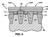
ゲート間誘電層78を通るFG-FG静電容量82を増加するという悪影響も有する。従って、より高誘電率の材料がゲート間誘電層78として利用されるにつれ、FG-FG静電容量82が増加する。本発明の実施形態は、図6−12に関して以下にさらに説明されるように、ゲート間誘電層78を通る浮遊ゲート74間の容量性の経路を除去することによって、ゲート間誘電層78を通るFG-FG静電容量82を削減し得る。
持つ材料をあらわす。ゲート間誘電層120のために利用され得る適切な高誘電率材料は、Al2O3、Gd2O3、Yb2O3、Dy2O3、Nb2O5、Y2O3、La2O3、ZrO2、HfO2、TiO2、Ta2O5、SrTiO3、BaxSr1-xTiO3、ZrxSi1-xOy、HfxSi1-xOy、もしくはAlxZr1-xO2、あるいはそれらの組み合わせを含むが限定はされない。前述の通り、高誘電率誘電材料を利用することで、浮遊ゲートトランジスタ内のゲート間誘電体の厚みが非常に薄い場合でさえも、トランジスタ性能を維持しながらゲートリークを削減する。
Claims (3)
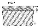
- 基板の上にゲート酸化物層を配置するステップと、
前記ゲート酸化物層の上に浮遊ゲート層を配置するステップと、
前記浮遊ゲート層の上にゲート間誘電層を配置するステップと、
複数の分離されているゲート間誘電領域を形成するために、前記ゲート間誘電層、前記浮遊ゲート層、前記ゲート酸化物層、および前記基板の各々を通して、複数の実質的に平行なトレンチを同じ処理段階でエッチングするステップと、
前記複数のトレンチの各々を絶縁酸化物で充填するステップと、
前記絶縁酸化物と前記複数の分離されているゲート間誘電領域とを平坦化するステップと、
平坦化された前記ゲート間誘電領域の各々の上に制御ゲートを堆積するステップと、
を含む、浮遊ゲートメモリアレイを製造する方法。 - エッチングするステップが、前記ゲート間誘電層と、前記浮遊ゲート層の各々を単一の処理段階でエッチングするステップを含む、請求項1に記載の方法。
- 前記絶縁酸化物と前記複数の分離されているゲート間誘電領域とを平坦化する前記ステップは、前記浮遊ゲート層の絶縁領域によって分離される絶縁酸化物領域を作るために、前記複数のトレンチの各々を絶縁酸化物で充填するステップの後、前記絶縁酸化物と前記複数の分離されているゲート間誘電領域とを平坦化するステップを含む、請求項1に記載の方法。
Applications Claiming Priority (3)
| Application Number | Priority Date | Filing Date | Title |
|---|---|---|---|
| US11/471,772 US7977190B2 (en) | 2006-06-21 | 2006-06-21 | Memory devices having reduced interference between floating gates and methods of fabricating such devices |
| US11/471,772 | 2006-06-21 | ||
| PCT/US2007/014431 WO2007149515A2 (en) | 2006-06-21 | 2007-06-20 | Floating gate memory devices and fabrication |
Publications (3)
| Publication Number | Publication Date |
|---|---|
| JP2009541999A JP2009541999A (ja) | 2009-11-26 |
| JP2009541999A5 JP2009541999A5 (ja) | 2010-04-30 |
| JP5801030B2 true JP5801030B2 (ja) | 2015-10-28 |
Family
ID=38669533
Family Applications (1)
| Application Number | Title | Priority Date | Filing Date |
|---|---|---|---|
| JP2009516566A Active JP5801030B2 (ja) | 2006-06-21 | 2007-06-20 | 浮遊ゲートメモリデバイスと製造 |
Country Status (6)
| Country | Link |
|---|---|
| US (3) | US7977190B2 (ja) |
| EP (1) | EP2036122A2 (ja) |
| JP (1) | JP5801030B2 (ja) |
| KR (1) | KR101350632B1 (ja) |
| CN (1) | CN101473429B (ja) |
| WO (1) | WO2007149515A2 (ja) |
Families Citing this family (8)
| Publication number | Priority date | Publication date | Assignee | Title |
|---|---|---|---|---|
| US7763933B2 (en) | 2007-02-15 | 2010-07-27 | Micron Technology, Inc. | Transistor constructions and processing methods |
| US7948021B2 (en) | 2007-04-27 | 2011-05-24 | Kabushiki Kaisha Toshiba | Semiconductor memory device and method of fabricating the same |
| US20080273410A1 (en) * | 2007-05-04 | 2008-11-06 | Jaydeb Goswami | Tungsten digitlines |
| JP4594973B2 (ja) | 2007-09-26 | 2010-12-08 | 株式会社東芝 | 不揮発性半導体記憶装置 |
| US8750040B2 (en) | 2011-01-21 | 2014-06-10 | Micron Technology, Inc. | Memory devices having source lines directly coupled to body regions and methods |
| CN102184869B (zh) * | 2011-04-28 | 2015-07-08 | 上海华虹宏力半导体制造有限公司 | Mos晶体管隔离区制造方法及mos晶体管 |
| CN105304549A (zh) * | 2014-07-29 | 2016-02-03 | 盛美半导体设备(上海)有限公司 | 浅沟槽隔离结构的形成方法 |
| JP2018537866A (ja) * | 2015-11-03 | 2018-12-20 | シリコン ストーリッジ テクノロージー インコーポレイテッドSilicon Storage Technology, Inc. | 不揮発性メモリにおける金属浮遊ゲートの集積 |
Family Cites Families (25)
| Publication number | Priority date | Publication date | Assignee | Title |
|---|---|---|---|---|
| US6781895B1 (en) | 1991-12-19 | 2004-08-24 | Kabushiki Kaisha Toshiba | Non-volatile semiconductor memory device and memory system using the same |
| JP3469362B2 (ja) | 1994-08-31 | 2003-11-25 | 株式会社東芝 | 半導体記憶装置 |
| US5622881A (en) * | 1994-10-06 | 1997-04-22 | International Business Machines Corporation | Packing density for flash memories |
| JP3583579B2 (ja) * | 1997-06-06 | 2004-11-04 | 株式会社東芝 | 不揮発性半導体記憶装置およびその製造方法 |
| JP4237344B2 (ja) * | 1998-09-29 | 2009-03-11 | 株式会社東芝 | 半導体装置及びその製造方法 |
| US6228713B1 (en) * | 1999-06-28 | 2001-05-08 | Chartered Semiconductor Manufacturing Ltd. | Self-aligned floating gate for memory application using shallow trench isolation |
| US6461915B1 (en) | 1999-09-01 | 2002-10-08 | Micron Technology, Inc. | Method and structure for an improved floating gate memory cell |
| JP2002076272A (ja) * | 2000-08-23 | 2002-03-15 | Sony Corp | 半導体装置の製造方法 |
| JP3984020B2 (ja) * | 2000-10-30 | 2007-09-26 | 株式会社東芝 | 不揮発性半導体記憶装置 |
| US6656852B2 (en) * | 2001-12-06 | 2003-12-02 | Texas Instruments Incorporated | Method for the selective removal of high-k dielectrics |
| US6795326B2 (en) | 2001-12-12 | 2004-09-21 | Micron Technology, Inc. | Flash array implementation with local and global bit lines |
| KR100462175B1 (ko) * | 2002-02-08 | 2004-12-16 | 삼성전자주식회사 | 부유게이트를 갖는 비휘발성 메모리 소자의 셀 및 그제조방법 |
| KR100537277B1 (ko) * | 2002-11-27 | 2005-12-19 | 주식회사 하이닉스반도체 | 반도체 소자의 제조 방법 |
| KR100501464B1 (ko) | 2003-02-04 | 2005-07-18 | 동부아남반도체 주식회사 | 비휘발성 메모리 장치 제조 방법 |
| JP3923926B2 (ja) * | 2003-07-04 | 2007-06-06 | 株式会社東芝 | 半導体記憶装置 |
| JP4237561B2 (ja) | 2003-07-04 | 2009-03-11 | 株式会社東芝 | 半導体記憶装置及びその製造方法 |
| JP3998622B2 (ja) | 2003-09-30 | 2007-10-31 | 株式会社東芝 | 不揮発性半導体記憶装置およびその製造方法 |
| US6982905B2 (en) | 2003-10-09 | 2006-01-03 | Micron Technology, Inc. | Method and apparatus for reading NAND flash memory array |
| US6996004B1 (en) | 2003-11-04 | 2006-02-07 | Advanced Micro Devices, Inc. | Minimization of FG-FG coupling in flash memory |
| KR20050048114A (ko) | 2003-11-19 | 2005-05-24 | 주식회사 하이닉스반도체 | 플래쉬 메모리 소자의 제조 방법 |
| US7045419B2 (en) * | 2003-12-12 | 2006-05-16 | Macronix International Co., Ltd. | Elimination of the fast-erase phenomena in flash memory |
| JP2005209931A (ja) * | 2004-01-23 | 2005-08-04 | Renesas Technology Corp | 不揮発性半導体記憶装置およびその製造方法 |
| US6951790B1 (en) | 2004-03-24 | 2005-10-04 | Micron Technology, Inc. | Method of forming select lines for NAND memory devices |
| US7332408B2 (en) * | 2004-06-28 | 2008-02-19 | Micron Technology, Inc. | Isolation trenches for memory devices |
| JP2007096151A (ja) * | 2005-09-30 | 2007-04-12 | Toshiba Corp | 半導体記憶装置およびその製造方法 |
-
2006
- 2006-06-21 US US11/471,772 patent/US7977190B2/en active Active
-
2007
- 2007-06-20 WO PCT/US2007/014431 patent/WO2007149515A2/en active Application Filing
- 2007-06-20 KR KR1020097001240A patent/KR101350632B1/ko active IP Right Grant
- 2007-06-20 CN CN200780022954.0A patent/CN101473429B/zh active Active
- 2007-06-20 EP EP07809749A patent/EP2036122A2/en not_active Ceased
- 2007-06-20 JP JP2009516566A patent/JP5801030B2/ja active Active
-
2011
- 2011-07-11 US US13/180,361 patent/US8441058B2/en active Active
-
2013
- 2013-04-19 US US13/866,698 patent/US9018059B2/en active Active
Also Published As
| Publication number | Publication date |
|---|---|
| WO2007149515A3 (en) | 2008-02-21 |
| WO2007149515A2 (en) | 2007-12-27 |
| US7977190B2 (en) | 2011-07-12 |
| US20110266610A1 (en) | 2011-11-03 |
| KR101350632B1 (ko) | 2014-01-10 |
| KR20090034892A (ko) | 2009-04-08 |
| US8441058B2 (en) | 2013-05-14 |
| CN101473429A (zh) | 2009-07-01 |
| CN101473429B (zh) | 2011-08-03 |
| US9018059B2 (en) | 2015-04-28 |
| JP2009541999A (ja) | 2009-11-26 |
| EP2036122A2 (en) | 2009-03-18 |
| US20070296015A1 (en) | 2007-12-27 |
| US20130237031A1 (en) | 2013-09-12 |
Similar Documents
| Publication | Publication Date | Title |
|---|---|---|
| JP5801030B2 (ja) | 浮遊ゲートメモリデバイスと製造 | |
| US7453134B2 (en) | Integrated circuit device with a circuit element formed on an active region having rounded corners | |
| US7569468B2 (en) | Method for forming a floating gate memory with polysilicon local interconnects | |
| US7344942B2 (en) | Isolation regions for semiconductor devices and their formation | |
| US20230223461A1 (en) | Semiconductor Constructions, Methods Of Forming Transistor Gates, And Methods Of Forming NAND Cell Units | |
| US9076824B2 (en) | Memory arrays with a memory cell adjacent to a smaller size of a pillar having a greater channel length than a memory cell adjacent to a larger size of the pillar and methods | |
| US8618597B2 (en) | Transistor constructions and processing methods | |
| US7115458B2 (en) | Gate coupling in floating-gate memory cells | |
| US7348236B2 (en) | Formation of memory cells and select gates of NAND memory arrays | |
| KR100990024B1 (ko) | 플래시 기술을 위한 제어 게이트 측면 | |
| US20060043368A1 (en) | Flash cell structures and methods of formation |
Legal Events
| Date | Code | Title | Description |
|---|---|---|---|
| A521 | Request for written amendment filed |
Free format text: JAPANESE INTERMEDIATE CODE: A821 Effective date: 20100303 Free format text: JAPANESE INTERMEDIATE CODE: A523 Effective date: 20100303 |
|
| A621 | Written request for application examination |
Free format text: JAPANESE INTERMEDIATE CODE: A621 Effective date: 20100303 |
|
| A977 | Report on retrieval |
Free format text: JAPANESE INTERMEDIATE CODE: A971007 Effective date: 20120822 |
|
| A131 | Notification of reasons for refusal |
Free format text: JAPANESE INTERMEDIATE CODE: A131 Effective date: 20120828 |
|
| A521 | Request for written amendment filed |
Free format text: JAPANESE INTERMEDIATE CODE: A523 Effective date: 20121128 Free format text: JAPANESE INTERMEDIATE CODE: A821 Effective date: 20121128 |
|
| A131 | Notification of reasons for refusal |
Free format text: JAPANESE INTERMEDIATE CODE: A131 Effective date: 20130604 |
|
| A521 | Request for written amendment filed |
Free format text: JAPANESE INTERMEDIATE CODE: A821 Effective date: 20130904 Free format text: JAPANESE INTERMEDIATE CODE: A523 Effective date: 20130904 |
|
| A02 | Decision of refusal |
Free format text: JAPANESE INTERMEDIATE CODE: A02 Effective date: 20140304 |
|
| A521 | Request for written amendment filed |
Free format text: JAPANESE INTERMEDIATE CODE: A523 Effective date: 20140704 Free format text: JAPANESE INTERMEDIATE CODE: A821 Effective date: 20140704 |
|
| A911 | Transfer to examiner for re-examination before appeal (zenchi) |
Free format text: JAPANESE INTERMEDIATE CODE: A911 Effective date: 20140714 |
|
| A912 | Re-examination (zenchi) completed and case transferred to appeal board |
Free format text: JAPANESE INTERMEDIATE CODE: A912 Effective date: 20140905 |
|
| A521 | Request for written amendment filed |
Free format text: JAPANESE INTERMEDIATE CODE: A821 Effective date: 20140919 |
|
| A521 | Request for written amendment filed |
Free format text: JAPANESE INTERMEDIATE CODE: A821 Effective date: 20141107 |
|
| A521 | Request for written amendment filed |
Free format text: JAPANESE INTERMEDIATE CODE: A523 Effective date: 20150722 Free format text: JAPANESE INTERMEDIATE CODE: A821 Effective date: 20150722 |
|
| A61 | First payment of annual fees (during grant procedure) |
Free format text: JAPANESE INTERMEDIATE CODE: A61 Effective date: 20150826 |
|
| R150 | Certificate of patent or registration of utility model |
Ref document number: 5801030 Country of ref document: JP Free format text: JAPANESE INTERMEDIATE CODE: R150 |
|
| R250 | Receipt of annual fees |
Free format text: JAPANESE INTERMEDIATE CODE: R250 |
|
| R250 | Receipt of annual fees |
Free format text: JAPANESE INTERMEDIATE CODE: R250 |
|
| R250 | Receipt of annual fees |
Free format text: JAPANESE INTERMEDIATE CODE: R250 |
|
| R250 | Receipt of annual fees |
Free format text: JAPANESE INTERMEDIATE CODE: R250 |
|
| R250 | Receipt of annual fees |
Free format text: JAPANESE INTERMEDIATE CODE: R250 |
|
| R250 | Receipt of annual fees |
Free format text: JAPANESE INTERMEDIATE CODE: R250 |