JP5779894B2 - 通信装置及び画像処理装置 - Google Patents
通信装置及び画像処理装置 Download PDFInfo
- Publication number
- JP5779894B2 JP5779894B2 JP2011020166A JP2011020166A JP5779894B2 JP 5779894 B2 JP5779894 B2 JP 5779894B2 JP 2011020166 A JP2011020166 A JP 2011020166A JP 2011020166 A JP2011020166 A JP 2011020166A JP 5779894 B2 JP5779894 B2 JP 5779894B2
- Authority
- JP
- Japan
- Prior art keywords
- communication unit
- mode
- packet
- request packet
- unit
- Prior art date
- Legal status (The legal status is an assumption and is not a legal conclusion. Google has not performed a legal analysis and makes no representation as to the accuracy of the status listed.)
- Active
Links
- 238000004891 communication Methods 0.000 title claims description 161
- 238000012545 processing Methods 0.000 title claims description 44
- 230000004044 response Effects 0.000 claims description 114
- 238000000034 method Methods 0.000 claims description 104
- 230000008569 process Effects 0.000 claims description 102
- 230000007704 transition Effects 0.000 claims description 62
- 230000005012 migration Effects 0.000 claims description 40
- 238000013508 migration Methods 0.000 claims description 40
- 230000000717 retained effect Effects 0.000 claims description 6
- 230000006870 function Effects 0.000 description 16
- 238000012546 transfer Methods 0.000 description 7
- 238000004364 calculation method Methods 0.000 description 6
- 238000010586 diagram Methods 0.000 description 6
- 230000005540 biological transmission Effects 0.000 description 5
- 238000009825 accumulation Methods 0.000 description 1
- 230000008901 benefit Effects 0.000 description 1
- 125000004122 cyclic group Chemical group 0.000 description 1
- 238000012986 modification Methods 0.000 description 1
- 230000004048 modification Effects 0.000 description 1
- 230000002093 peripheral effect Effects 0.000 description 1
- 238000005316 response function Methods 0.000 description 1
Images


Classifications
-
- Y—GENERAL TAGGING OF NEW TECHNOLOGICAL DEVELOPMENTS; GENERAL TAGGING OF CROSS-SECTIONAL TECHNOLOGIES SPANNING OVER SEVERAL SECTIONS OF THE IPC; TECHNICAL SUBJECTS COVERED BY FORMER USPC CROSS-REFERENCE ART COLLECTIONS [XRACs] AND DIGESTS
- Y02—TECHNOLOGIES OR APPLICATIONS FOR MITIGATION OR ADAPTATION AGAINST CLIMATE CHANGE
- Y02D—CLIMATE CHANGE MITIGATION TECHNOLOGIES IN INFORMATION AND COMMUNICATION TECHNOLOGIES [ICT], I.E. INFORMATION AND COMMUNICATION TECHNOLOGIES AIMING AT THE REDUCTION OF THEIR OWN ENERGY USE
- Y02D10/00—Energy efficient computing, e.g. low power processors, power management or thermal management
Landscapes
- Accessory Devices And Overall Control Thereof (AREA)
- Control Or Security For Electrophotography (AREA)
- Power Sources (AREA)
- Facsimiles In General (AREA)
Description
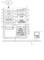
10 プリンタ
11 スキャナ
12 NCU
13 モデム
14 NIC
20 電力制御部
21 バックエンド部
22 フロントエンド部
Claims (4)
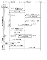
- 待機モード及び該待機モードより消費電力量が小さい省電力モードを含む電力モードの移行制御を行う電力制御部と、
外部機器から要求パケットを受信する第1の通信部と、
前記待機モードにおいて、前記第1の通信部によって受信された要求パケットに対して応答パケットを返信し、前記省電力モードにおいて、少なくとも一部に対する通電が前記電力制御部によって停止されることにより、前記応答パケットの返信が不可能となる第2の通信部と、
を備え、
前記第1の通信部は、前記第2の通信部において前記待機モードから前記省電力モードへのシャットダウン処理を含む移行処理が実行されている最中に、前記要求パケットを受信した場合、該要求パケットを保持し、該要求パケットを保持した状態で、前記第2の通信部による前記シャットダウン処理を含む移行処理が完了した場合、前記電力モードを前記待機モードに復帰させる復帰指示を出力し、前記待機モードに復帰した後、保持していた前記要求パケットを前記第2の通信部へ出力し、
前記電力制御部は、前記第1の通信部によって出力された復帰指示に従って、前記電力モードを前記待機モードに復帰させ、
前記第2の通信部は、復帰後、前記第1の通信部によって出力された前記要求パケットに対する前記応答パケットを返信し、
かつ、
前記第2の通信部は、前記シャットダウン処理を開始する際に、前記第1の通信部の通信制御モードを移行制御モードに切り替えさせる切替指示を前記第1の通信部へ出力し、前記シャットダウン処理が完了した後に、前記第1の通信部の通信制御モードを通常制御モードに切り替えさせる切替指示を前記第1の通信部へ出力し、
前記第1の通信部は、
前記第2の通信部から前記移行制御モードに切り替えさせる切替指示が出力された場合、前記通信制御モードを前記移行制御モードに切り替え、前記通常制御モードに切り替えさせる切替指示が出力された場合、前記通信制御モードを前記通常制御モードへ切り替え、
前記移行制御モードにおいて、前記要求パケットを受信した場合、該要求パケットを保持し、前記通常制御モードに切り替えた際に前記要求パケットを保持している場合、前記復帰指示を出力することを特徴とする通信装置。 - 前記第1の通信部は、前記第2の通信部において前記シャットダウン処理を含む移行処理が実行されている最中に、前記第1の通信部によって応答可能な前記要求パケットを受信した場合、前記応答パケットを返信し、前記第1の通信部によって応答不可能な前記要求パケットを受信した場合、該要求パケットを保持することを特徴とする請求項1に記載の通信装置。
- 前記第1の通信部は、前記省電力モードにおいて、前記第1の通信部によって応答可能な前記要求パケットを受信した場合、前記応答パケットを返信し、前記第1の通信部によって応答不可能な前記要求パケットを受信した場合、前記電力モードを前記待機モードに復帰させる復帰指示を出力し、
前記電力制御部は、前記第1の通信部によって出力された復帰指示に従って、前記電力モードを前記待機モードに復帰させ、
前記第2の通信部は、復帰後、前記第1の通信部によって前記省電力モードにおいて受信された要求パケットに対する前記応答パケットを返信することを特徴とする請求項1又は2に記載の通信装置。 - 請求項1〜3のいずれか1項に記載の通信装置と、
画像処理を行う処理部と、を備え、
前記第1の通信部は、前記外部機器から画像処理の要求を行う前記要求パケットを受信し、
前記処理部は、前記要求パケットに応じて画像処理を行うことを特徴とする画像処理装置。
Priority Applications (1)
| Application Number | Priority Date | Filing Date | Title |
|---|---|---|---|
| JP2011020166A JP5779894B2 (ja) | 2011-02-01 | 2011-02-01 | 通信装置及び画像処理装置 |
Applications Claiming Priority (1)
| Application Number | Priority Date | Filing Date | Title |
|---|---|---|---|
| JP2011020166A JP5779894B2 (ja) | 2011-02-01 | 2011-02-01 | 通信装置及び画像処理装置 |
Publications (2)
| Publication Number | Publication Date |
|---|---|
| JP2012160974A JP2012160974A (ja) | 2012-08-23 |
| JP5779894B2 true JP5779894B2 (ja) | 2015-09-16 |
Family
ID=46841132
Family Applications (1)
| Application Number | Title | Priority Date | Filing Date |
|---|---|---|---|
| JP2011020166A Active JP5779894B2 (ja) | 2011-02-01 | 2011-02-01 | 通信装置及び画像処理装置 |
Country Status (1)
| Country | Link |
|---|---|
| JP (1) | JP5779894B2 (ja) |
Families Citing this family (6)
| Publication number | Priority date | Publication date | Assignee | Title |
|---|---|---|---|---|
| JP5630339B2 (ja) * | 2011-03-14 | 2014-11-26 | 村田機械株式会社 | 通信装置及び画像処理装置 |
| JP2014075786A (ja) * | 2012-09-11 | 2014-04-24 | Canon Inc | 画像形成装置、画像形成装置の制御方法、及び、プログラム |
| JP6210753B2 (ja) | 2013-06-24 | 2017-10-11 | キヤノン株式会社 | 情報処理装置 |
| JP6336328B2 (ja) * | 2014-05-02 | 2018-06-06 | キヤノン株式会社 | 通信装置とその制御方法、及びプログラム |
| JP6632673B2 (ja) * | 2018-08-31 | 2020-01-22 | キヤノン株式会社 | 印刷装置およびその制御方法 |
| JP7424479B2 (ja) * | 2020-05-21 | 2024-01-30 | 日本電信電話株式会社 | 電源管理装置、電源管理システム、電源管理方法、および、電源管理プログラム |
Family Cites Families (4)
| Publication number | Priority date | Publication date | Assignee | Title |
|---|---|---|---|---|
| JP3703431B2 (ja) * | 2001-01-24 | 2005-10-05 | キヤノン株式会社 | データ通信装置、画像処理装置、データ通信方法、及び画像処理装置におけるデータ通信方法 |
| JP5188051B2 (ja) * | 2006-10-12 | 2013-04-24 | キヤノン株式会社 | 表示制御装置及び表示装置 |
| JP2010280093A (ja) * | 2009-06-03 | 2010-12-16 | Brother Ind Ltd | 通信装置 |
| JP5377091B2 (ja) * | 2009-06-05 | 2013-12-25 | キヤノン株式会社 | 情報処理装置及びその制御方法 |
-
2011
- 2011-02-01 JP JP2011020166A patent/JP5779894B2/ja active Active
Also Published As
| Publication number | Publication date |
|---|---|
| JP2012160974A (ja) | 2012-08-23 |
Similar Documents
| Publication | Publication Date | Title |
|---|---|---|
| US10110764B2 (en) | Image forming apparatus that shifts into different power saving states and control method thereof | |
| JP4217445B2 (ja) | データ処理装置および電力制御方法およびコンピュータが読み取り可能な記憶媒体およびプログラム | |
| US8423810B2 (en) | Network interface apparatus | |
| JP5779894B2 (ja) | 通信装置及び画像処理装置 | |
| US8793513B2 (en) | Network device | |
| US20200195803A1 (en) | Image processing system, image processing apparatus, cloud server, and program | |
| US20110134477A1 (en) | Network Printer | |
| JP5630339B2 (ja) | 通信装置及び画像処理装置 | |
| JP2012175496A (ja) | 画像形成装置及びプログラム | |
| US9569145B2 (en) | Gateway apparatus | |
| JP2012227730A (ja) | 通信装置 | |
| JP2012160086A (ja) | データ処理装置、クライアント装置、及びデータ処理システム | |
| JP5636806B2 (ja) | ネットワーク複合機 | |
| JP6460346B2 (ja) | 電子機器および電力制御プログラム | |
| JP2009303007A (ja) | インターネットファクシミリ装置及び画像形成装置 | |
| JP2010273227A (ja) | ネットワーク通信装置 | |
| JP5678497B2 (ja) | ネットワークプリンタ | |
| JP5817287B2 (ja) | 情報処理装置と情報処理方法とプログラム | |
| JP5617661B2 (ja) | 通信装置 | |
| JP5672633B2 (ja) | 通信端末装置 | |
| JP6439939B2 (ja) | 電子機器および電力制御プログラム | |
| JP5664702B2 (ja) | ネットワーク通信装置 | |
| JP5609409B2 (ja) | ネットワーク複合機 | |
| JP6341383B2 (ja) | 電子機器および電力制御プログラム | |
| JP2011060047A (ja) | 画像処理装置および電力制御方法 |
Legal Events
| Date | Code | Title | Description |
|---|---|---|---|
| A621 | Written request for application examination |
Free format text: JAPANESE INTERMEDIATE CODE: A621 Effective date: 20131224 |
|
| A977 | Report on retrieval |
Free format text: JAPANESE INTERMEDIATE CODE: A971007 Effective date: 20141126 |
|
| A131 | Notification of reasons for refusal |
Free format text: JAPANESE INTERMEDIATE CODE: A131 Effective date: 20150106 |
|
| A521 | Request for written amendment filed |
Free format text: JAPANESE INTERMEDIATE CODE: A523 Effective date: 20150303 |
|
| TRDD | Decision of grant or rejection written | ||
| A01 | Written decision to grant a patent or to grant a registration (utility model) |
Free format text: JAPANESE INTERMEDIATE CODE: A01 Effective date: 20150616 |
|
| A61 | First payment of annual fees (during grant procedure) |
Free format text: JAPANESE INTERMEDIATE CODE: A61 Effective date: 20150629 |
|
| R150 | Certificate of patent or registration of utility model |
Ref document number: 5779894 Country of ref document: JP Free format text: JAPANESE INTERMEDIATE CODE: R150 |
|
| R250 | Receipt of annual fees |
Free format text: JAPANESE INTERMEDIATE CODE: R250 |
|
| R250 | Receipt of annual fees |
Free format text: JAPANESE INTERMEDIATE CODE: R250 |
|
| R250 | Receipt of annual fees |
Free format text: JAPANESE INTERMEDIATE CODE: R250 |
|
| R250 | Receipt of annual fees |
Free format text: JAPANESE INTERMEDIATE CODE: R250 |
|
| R250 | Receipt of annual fees |
Free format text: JAPANESE INTERMEDIATE CODE: R250 |
|
| R250 | Receipt of annual fees |
Free format text: JAPANESE INTERMEDIATE CODE: R250 |