JP5723397B2 - プラズマ処理装置 - Google Patents
プラズマ処理装置 Download PDFInfo
- Publication number
- JP5723397B2 JP5723397B2 JP2013028902A JP2013028902A JP5723397B2 JP 5723397 B2 JP5723397 B2 JP 5723397B2 JP 2013028902 A JP2013028902 A JP 2013028902A JP 2013028902 A JP2013028902 A JP 2013028902A JP 5723397 B2 JP5723397 B2 JP 5723397B2
- Authority
- JP
- Japan
- Prior art keywords
- microwave
- processing
- plasma
- waveguide
- coaxial
- Prior art date
- Legal status (The legal status is an assumption and is not a legal conclusion. Google has not performed a legal analysis and makes no representation as to the accuracy of the status listed.)
- Expired - Fee Related
Links
- 238000012545 processing Methods 0.000 title claims description 112
- 239000004020 conductor Substances 0.000 claims description 33
- 238000000034 method Methods 0.000 claims description 25
- 230000005540 biological transmission Effects 0.000 claims description 23
- 239000000758 substrate Substances 0.000 claims description 22
- 230000008569 process Effects 0.000 claims description 16
- 238000009529 body temperature measurement Methods 0.000 claims description 3
- 239000007789 gas Substances 0.000 description 98
- 239000004065 semiconductor Substances 0.000 description 19
- 238000001020 plasma etching Methods 0.000 description 14
- 239000010453 quartz Substances 0.000 description 14
- VYPSYNLAJGMNEJ-UHFFFAOYSA-N silicon dioxide Inorganic materials O=[Si]=O VYPSYNLAJGMNEJ-UHFFFAOYSA-N 0.000 description 14
- 238000005530 etching Methods 0.000 description 8
- 239000003507 refrigerant Substances 0.000 description 8
- 229910052782 aluminium Inorganic materials 0.000 description 4
- XAGFODPZIPBFFR-UHFFFAOYSA-N aluminium Chemical compound [Al] XAGFODPZIPBFFR-UHFFFAOYSA-N 0.000 description 4
- 230000008878 coupling Effects 0.000 description 4
- 238000010168 coupling process Methods 0.000 description 4
- 238000005859 coupling reaction Methods 0.000 description 4
- 230000007246 mechanism Effects 0.000 description 4
- 238000012544 monitoring process Methods 0.000 description 4
- 230000001902 propagating effect Effects 0.000 description 4
- 230000002159 abnormal effect Effects 0.000 description 3
- 239000000498 cooling water Substances 0.000 description 3
- 150000002500 ions Chemical class 0.000 description 3
- 239000002245 particle Substances 0.000 description 3
- 238000012546 transfer Methods 0.000 description 3
- 239000003990 capacitor Substances 0.000 description 2
- 239000002826 coolant Substances 0.000 description 2
- 238000009826 distribution Methods 0.000 description 2
- 238000005259 measurement Methods 0.000 description 2
- 230000003287 optical effect Effects 0.000 description 2
- 230000002411 adverse Effects 0.000 description 1
- 230000008901 benefit Effects 0.000 description 1
- 230000000903 blocking effect Effects 0.000 description 1
- 238000005229 chemical vapour deposition Methods 0.000 description 1
- 238000011109 contamination Methods 0.000 description 1
- 238000001816 cooling Methods 0.000 description 1
- 239000003989 dielectric material Substances 0.000 description 1
- 238000009792 diffusion process Methods 0.000 description 1
- 230000005684 electric field Effects 0.000 description 1
- 238000000295 emission spectrum Methods 0.000 description 1
- 230000005284 excitation Effects 0.000 description 1
- -1 for example Substances 0.000 description 1
- 239000004047 hole gas Substances 0.000 description 1
- 238000002347 injection Methods 0.000 description 1
- 239000007924 injection Substances 0.000 description 1
- 239000004973 liquid crystal related substance Substances 0.000 description 1
- 238000004519 manufacturing process Methods 0.000 description 1
- 229910052751 metal Inorganic materials 0.000 description 1
- 239000002184 metal Substances 0.000 description 1
- 239000000203 mixture Substances 0.000 description 1
- 238000012986 modification Methods 0.000 description 1
- 230000004048 modification Effects 0.000 description 1
- 239000013307 optical fiber Substances 0.000 description 1
- 230000003647 oxidation Effects 0.000 description 1
- 238000007254 oxidation reaction Methods 0.000 description 1
- 238000005192 partition Methods 0.000 description 1
- 230000000149 penetrating effect Effects 0.000 description 1
- 238000005268 plasma chemical vapour deposition Methods 0.000 description 1
- 230000010287 polarization Effects 0.000 description 1
- 230000009467 reduction Effects 0.000 description 1
- 239000000523 sample Substances 0.000 description 1
- 238000001179 sorption measurement Methods 0.000 description 1
- 238000004611 spectroscopical analysis Methods 0.000 description 1
- 238000004544 sputter deposition Methods 0.000 description 1
- 229910001220 stainless steel Inorganic materials 0.000 description 1
- 239000010935 stainless steel Substances 0.000 description 1
- 238000009827 uniform distribution Methods 0.000 description 1
Images


Landscapes
- Plasma Technology (AREA)
- Chemical Vapour Deposition (AREA)
- Drying Of Semiconductors (AREA)
Description
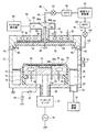
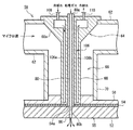
上記の装置構成においては、マイクロ波発生器より出力されたマイクロ波が導波管−同軸管変換器までは導波管の中をTEモードで伝播し、導波管−同軸管変換器から処理容器の誘電体板上のアンテナまでは同軸管の中をTEMモードで伝播して、アンテナから処理容器内の処理空間に導入されることにより、このマイクロ波のパワーにより処理ガスのガス粒子が電離して、プラズマが生成され、このプラズマの下で被処理基板に所望のプラズマ処理が施される。そして、処理容器内でプラズマ処理が行われている最中に、モニタ部が同軸管の内部導体である中空管の中を通り抜ける温度測定系ラインの先端に取り付けられる温度センサを通じて、処理容器内の上部天板中心付近の温度を測定する。
12 サセプタ(基板保持台)
26 排気装置
30 高周波電源
52 石英板(誘電体窓)
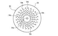
54 ラジアルラインスロットアンテナ
58 マイクロ波伝送線路
60 マイクロ波発生器
62 導波管
64 導波管−同軸管変換器
66 同軸管
68 内部導体
70 外部導体
82 処理ガス供給源
84 第1ガス供給管
86 上部中央ガス吐出孔
88 第1処理ガス導入部
94 第2処理ガス導入部
98 側部ガス吐出孔
100 第2ガス供給管
112 磁界形成部
114 モニタ部
Claims (2)
- 真空排気可能な処理容器内に被処理基板を収容し、前記処理容器内に処理ガスとマイクロ波のパワーを供給して前記処理ガスのプラズマを生成し、前記基板に所望のプラズマ処理を施すプラズマ処理装置であって、
前記マイクロ波を出力するマイクロ波発生器と;
前記マイクロ波発生器より出力された前記マイクロ波をTEモードで伝送する導波管と、前記処理容器の天井に設けられるマイクロ波導入用の誘電体板の上方で垂直に延びる同軸の内部導体と外部導体とを有し、前記マイクロ波をTEMモードで伝送する同軸管と、前記導波管と前記同軸管とを結合する導波管−同軸管変換器とを有するマイクロ波伝送線路と;
前記誘電体板の上で前記同軸管の終端に結合され、前記マイクロ波伝送線路より伝送されてきた前記マイクロ波を前記処理容器内に向けて放射するアンテナと;
を有し、
前記マイクロ波伝送線路の同軸管の内部導体を中空管に構成するとともに、前記誘電体板に前記中空管の管路と連通する貫通孔を設け、
前記中空管の管路および前記誘電体板の貫通孔をレーザ光路に用いて前記処理容器内のプロセスまたはプロセス条件の状態をモニタリングするモニタ部を備える、プラズマ処理装置。 - 真空排気可能な処理容器内に被処理基板を収容し、前記処理容器内に処理ガスとマイクロ波のパワーを供給して前記処理ガスのプラズマを生成し、前記基板に所望のプラズマ処理を施すプラズマ処理装置であって、
前記マイクロ波を出力するマイクロ波発生器と;
前記マイクロ波発生器より出力された前記マイクロ波をTEモードで伝送する導波管と、前記処理容器の天井に設けられるマイクロ波導入用の誘電体板の上方で垂直に延びる同軸の内部導体と外部導体とを有し、前記マイクロ波をTEMモードで伝送する同軸管と、前記導波管と前記同軸管とを結合する導波管−同軸管変換器とを有するマイクロ波伝送線路と;
前記誘電体板の上で前記同軸管の終端に結合され、前記マイクロ波伝送線路より伝送されてきた前記マイクロ波を前記処理容器内に向けて放射するアンテナと;
を有し、
前記マイクロ波伝送線路の同軸管の内部導体を中空管に構成し、
前記誘電体板に前記中空管の下端開口と連通する貫通孔を設け、
前記処理容器内の上部天板中心付近の温度を測定するために、前記中空管の中を通る温度測定系ラインと、この温度測定系ラインの先端に取り付けられる温度センサとを有するモニタ部を備える、プラズマ処理装置。
Priority Applications (1)
| Application Number | Priority Date | Filing Date | Title |
|---|---|---|---|
| JP2013028902A JP5723397B2 (ja) | 2013-02-18 | 2013-02-18 | プラズマ処理装置 |
Applications Claiming Priority (1)
| Application Number | Priority Date | Filing Date | Title |
|---|---|---|---|
| JP2013028902A JP5723397B2 (ja) | 2013-02-18 | 2013-02-18 | プラズマ処理装置 |
Related Parent Applications (1)
| Application Number | Title | Priority Date | Filing Date |
|---|---|---|---|
| JP2007088407A Division JP5438260B2 (ja) | 2007-03-29 | 2007-03-29 | プラズマ処理装置 |
Publications (2)
| Publication Number | Publication Date |
|---|---|
| JP2013118398A JP2013118398A (ja) | 2013-06-13 |
| JP5723397B2 true JP5723397B2 (ja) | 2015-05-27 |
Family
ID=48712704
Family Applications (1)
| Application Number | Title | Priority Date | Filing Date |
|---|---|---|---|
| JP2013028902A Expired - Fee Related JP5723397B2 (ja) | 2013-02-18 | 2013-02-18 | プラズマ処理装置 |
Country Status (1)
| Country | Link |
|---|---|
| JP (1) | JP5723397B2 (ja) |
Cited By (1)
| Publication number | Priority date | Publication date | Assignee | Title |
|---|---|---|---|---|
| CN100351402C (zh) * | 2003-08-05 | 2007-11-28 | 杰富意钢铁株式会社 | 钢材的制造方法及其制造设备 |
Families Citing this family (6)
| Publication number | Priority date | Publication date | Assignee | Title |
|---|---|---|---|---|
| US10601071B2 (en) | 2014-12-02 | 2020-03-24 | Polyplus Battery Company | Methods of making and inspecting a web of vitreous lithium sulfide separator sheet and lithium electrode assemblies |
| US10164289B2 (en) | 2014-12-02 | 2018-12-25 | Polyplus Battery Company | Vitreous solid electrolyte sheets of Li ion conducting sulfur-based glass and associated structures, cells and methods |
| US10147968B2 (en) | 2014-12-02 | 2018-12-04 | Polyplus Battery Company | Standalone sulfide based lithium ion-conducting glass solid electrolyte and associated structures, cells and methods |
| JP6698560B2 (ja) * | 2017-02-01 | 2020-05-27 | 東京エレクトロン株式会社 | マイクロ波プラズマ源、マイクロ波プラズマ処理装置、およびプラズマ処理方法 |
| US10679832B2 (en) * | 2017-07-10 | 2020-06-09 | Verity Instruments, Inc. | Microwave plasma source |
| US10923324B2 (en) | 2017-07-10 | 2021-02-16 | Verity Instruments, Inc. | Microwave plasma source |
Family Cites Families (2)
| Publication number | Priority date | Publication date | Assignee | Title |
|---|---|---|---|---|
| US6894245B2 (en) * | 2000-03-17 | 2005-05-17 | Applied Materials, Inc. | Merie plasma reactor with overhead RF electrode tuned to the plasma with arcing suppression |
| US7196283B2 (en) * | 2000-03-17 | 2007-03-27 | Applied Materials, Inc. | Plasma reactor overhead source power electrode with low arcing tendency, cylindrical gas outlets and shaped surface |
-
2013
- 2013-02-18 JP JP2013028902A patent/JP5723397B2/ja not_active Expired - Fee Related
Cited By (1)
| Publication number | Priority date | Publication date | Assignee | Title |
|---|---|---|---|---|
| CN100351402C (zh) * | 2003-08-05 | 2007-11-28 | 杰富意钢铁株式会社 | 钢材的制造方法及其制造设备 |
Also Published As
| Publication number | Publication date |
|---|---|
| JP2013118398A (ja) | 2013-06-13 |
Similar Documents
| Publication | Publication Date | Title |
|---|---|---|
| US10734197B2 (en) | Plasma process apparatus | |
| JP5438260B2 (ja) | プラズマ処理装置 | |
| JP5723397B2 (ja) | プラズマ処理装置 | |
| JP5368514B2 (ja) | プラズマ処理装置 | |
| US10063062B2 (en) | Method of detecting plasma discharge in a plasma processing system | |
| US8419960B2 (en) | Plasma processing apparatus and method | |
| KR102523730B1 (ko) | 이중 주파수 표면파 플라즈마 소스 | |
| US9761418B2 (en) | Plasma processing apparatus | |
| JP5522887B2 (ja) | プラズマ処理装置 | |
| US9646867B2 (en) | Plasma processing apparatus, power supply unit and mounting table system | |
| JP2005191056A (ja) | 処理装置 | |
| JP2013012353A (ja) | プラズマ処理装置 | |
| TW201411688A (zh) | 電漿處理裝置及電漿處理方法 | |
| CN115497801A (zh) | 基板处理装置及基板处理方法 | |
| JP2016058361A (ja) | プラズマ処理装置、及び光を検出する方法 | |
| US10665428B2 (en) | Plasma processing apparatus | |
| CN120656918A (zh) | 排气网、等离子体处理装置以及等离子体处理方法 | |
| JP2011176147A (ja) | プラズマ処理装置 |
Legal Events
| Date | Code | Title | Description |
|---|---|---|---|
| A977 | Report on retrieval |
Free format text: JAPANESE INTERMEDIATE CODE: A971007 Effective date: 20131024 |
|
| A131 | Notification of reasons for refusal |
Free format text: JAPANESE INTERMEDIATE CODE: A131 Effective date: 20140225 |
|
| A521 | Request for written amendment filed |
Free format text: JAPANESE INTERMEDIATE CODE: A523 Effective date: 20140415 |
|
| A131 | Notification of reasons for refusal |
Free format text: JAPANESE INTERMEDIATE CODE: A131 Effective date: 20141216 |
|
| A521 | Request for written amendment filed |
Free format text: JAPANESE INTERMEDIATE CODE: A523 Effective date: 20150206 |
|
| TRDD | Decision of grant or rejection written | ||
| A01 | Written decision to grant a patent or to grant a registration (utility model) |
Free format text: JAPANESE INTERMEDIATE CODE: A01 Effective date: 20150324 |
|
| A61 | First payment of annual fees (during grant procedure) |
Free format text: JAPANESE INTERMEDIATE CODE: A61 Effective date: 20150327 |
|
| R150 | Certificate of patent or registration of utility model |
Ref document number: 5723397 Country of ref document: JP Free format text: JAPANESE INTERMEDIATE CODE: R150 |
|
| R250 | Receipt of annual fees |
Free format text: JAPANESE INTERMEDIATE CODE: R250 |
|
| R250 | Receipt of annual fees |
Free format text: JAPANESE INTERMEDIATE CODE: R250 |
|
| R250 | Receipt of annual fees |
Free format text: JAPANESE INTERMEDIATE CODE: R250 |
|
| R250 | Receipt of annual fees |
Free format text: JAPANESE INTERMEDIATE CODE: R250 |
|
| LAPS | Cancellation because of no payment of annual fees |