JP5679236B2 - パーティションを設けたスキャン・チェーンを備えた集積回路のスキャンテストにおける向上した制御 - Google Patents
パーティションを設けたスキャン・チェーンを備えた集積回路のスキャンテストにおける向上した制御 Download PDFInfo
- Publication number
- JP5679236B2 JP5679236B2 JP2012535422A JP2012535422A JP5679236B2 JP 5679236 B2 JP5679236 B2 JP 5679236B2 JP 2012535422 A JP2012535422 A JP 2012535422A JP 2012535422 A JP2012535422 A JP 2012535422A JP 5679236 B2 JP5679236 B2 JP 5679236B2
- Authority
- JP
- Japan
- Prior art keywords
- input
- output
- register
- scan
- partition
- Prior art date
- Legal status (The legal status is an assumption and is not a legal conclusion. Google has not performed a legal analysis and makes no representation as to the accuracy of the status listed.)
- Active
Links
- 238000012360 testing method Methods 0.000 title claims description 161
- 238000005192 partition Methods 0.000 claims description 175
- 230000006870 function Effects 0.000 claims description 6
- 230000000875 corresponding effect Effects 0.000 description 61
- 239000013598 vector Substances 0.000 description 52
- 238000010586 diagram Methods 0.000 description 39
- 230000007704 transition Effects 0.000 description 23
- 230000004044 response Effects 0.000 description 20
- 238000013459 approach Methods 0.000 description 15
- 230000006835 compression Effects 0.000 description 6
- 238000007906 compression Methods 0.000 description 6
- 238000013461 design Methods 0.000 description 3
- 238000000034 method Methods 0.000 description 3
- 230000001934 delay Effects 0.000 description 2
- 230000003111 delayed effect Effects 0.000 description 2
- 238000011156 evaluation Methods 0.000 description 2
- 230000001360 synchronised effect Effects 0.000 description 2
- 230000001960 triggered effect Effects 0.000 description 2
- 241001455213 Leopardus pardalis Species 0.000 description 1
- 230000002411 adverse Effects 0.000 description 1
- 230000002596 correlated effect Effects 0.000 description 1
- 230000006837 decompression Effects 0.000 description 1
- 230000000694 effects Effects 0.000 description 1
- 238000013100 final test Methods 0.000 description 1
- 230000004927 fusion Effects 0.000 description 1
- 230000002441 reversible effect Effects 0.000 description 1
- 230000000630 rising effect Effects 0.000 description 1
Images


Classifications
-
- G—PHYSICS
- G01—MEASURING; TESTING
- G01R—MEASURING ELECTRIC VARIABLES; MEASURING MAGNETIC VARIABLES
- G01R31/00—Arrangements for testing electric properties; Arrangements for locating electric faults; Arrangements for electrical testing characterised by what is being tested not provided for elsewhere
- G01R31/28—Testing of electronic circuits, e.g. by signal tracer
- G01R31/317—Testing of digital circuits
- G01R31/3181—Functional testing
- G01R31/3185—Reconfiguring for testing, e.g. LSSD, partitioning
- G01R31/318533—Reconfiguring for testing, e.g. LSSD, partitioning using scanning techniques, e.g. LSSD, Boundary Scan, JTAG
Landscapes
- Engineering & Computer Science (AREA)
- General Engineering & Computer Science (AREA)
- Physics & Mathematics (AREA)
- General Physics & Mathematics (AREA)
- Tests Of Electronic Circuits (AREA)
- Semiconductor Integrated Circuits (AREA)
- Test And Diagnosis Of Digital Computers (AREA)
Description
1.例示の環境
2.集積回路
3.パーティション・セレクタ
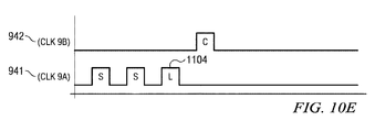
4.パーティション・スキャン・イネーブルのタイミング図
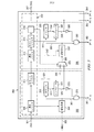
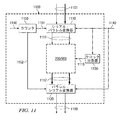
図5は、本発明の一実施例におけるテスト・コントローラのブロック図である。テスト・コントローラ500(図2でも270で示す)は、パーティション・セレクタ300、ANDゲート520A〜520D及び530A〜530D、及びレジスタ540A〜540Dを含むよう示されている。これは、各パーティションを制御するために用いられる1つの候補となり得る実施例であるが、他の実施例が、(テスト・コントローラを用いるのではなく)デバイス・ピンから直接情報を提供すること、又はデバイス・ピンとテスト・コントローラとの間の制御を配分することを含んでいてもよい。
6.テスト・ベクトル生成
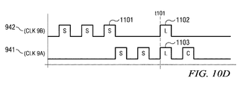
7.ローンチ・オフ・キャプチャ・テストのタイミング図
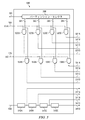
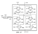
図9は、本発明の別の実施例において、LOS(launch off shift)遷移故障テストをサポートしつつ、電力消費が低減されるなどの向上した制御の利点を提供し、テストカバレッジ又はテスト適用時間が低減された又はそれらに影響を与えない、ICのブロック図である。IC900は、レジスタ(又は、一般に、ストレージ要素)910A及び910B、MUX920A及び920B、ディコンプレッサー930A及び930B、パーティション940A及び940B、圧縮器950A及び950B、及びMUX960を含むよう示されている。簡潔にしかつ説明を簡単にするため、2つのパーティション及び対応する回路(ディコンプレッサー、圧縮器、など)のみを図9に示す。しかし、代替の実施例が、本発明の幾つかの側面の範囲及び趣旨から逸脱することなく、2つ以上のパーティション(対応するディコンプレッサー、圧縮器、及びレジスタと共に)を備えて実装されてもよい。
9.テスト・ピン数の低減
s1は、Sel[1:0]の状態00を表す
s2は、Sel[1:0]の状態01を表す
s3は、Sel[1:0]の状態10を表す
s4は、Sel[1:0]の状態11を表す
Claims (4)
- 集積回路であって、
複数のスキャン・チェーンとして機能し得る複数のメモリ要素であって、前記複数のスキャン・チェーンが複数のパーティションにグループ化されて、それにより各パーティションの複数のスキャン・チェーンが対応するパーティション・イネーブル信号を介して共にイネーブルされ、各スキャン・チェーンがテスト・データを受けるためのテスト・データ入力に接続される、前記複数のメモリ要素と、
複数のブロックを含むテスト・コントローラであって、各ブロックが前記複数のパーティションの1つに対応する、テスト・コントローラと、
を含み、
各ブロックが、
その中にデジタル・データを格納する遅延レジスタであって、デジタル・データ入力を受ける入力とデジタル・データ出力を発生する出力とを有する、前記遅延レジスタと、
その中にデジタル・カウントを格納するカウント・レジスタであって、前記対応する遅延レジスタの前記出力に接続された入力とデジタル・データ出力を発生する出力とを有する、前記カウント・レジスタと、
対応する遅延レジスタに格納された前記デジタル・データを受ける第1の入力と、第2の入力と、前記第2の入力で入力を受けた後の所定の時間に所定の状態を有するデジタル・データ出力を発生する出力とを有する遅延要素であって、前記所定の時間が対応する遅延レジスタに格納された前記デジタル・データに対応する、前記遅延要素と、
前記遅延要素の前記出力に接続されたトリガ入力とその中のカウントに対応するデジタル出力を発生するカウント出力とを有するカウンタであって、前記トリガ入力で所定の状態の受信の開始をカウントする、前記カウンタと、
前記カウント・レジスタと前記カウンタに接続された比較器であって、前記カウント・レジスタに格納された前記デジタル・カウントを前記カウンタの前記カウントと比較し、前記カウント・レジスタに格納されたデジタル・カウントが前記カウンタの前記カウントと一致するときに一致信号を発生する、前記比較器と、
前記比較器の前記一致信号を入力するための入力と、出力とを有するインバータと、
前記遅延要素の前記出力を受けるように接続された第1の入力と、前記インバータの前記出力を受けるように接続された第2の入力と、複数のスキャン・チェーンの対応するパーティションに対する前記パーティション・イネーブル信号を発生する出力とを有するANDゲートと、
を含み、
前記テスト・コントローラの前記複数のブロックが第1のブロックから最後のブロックに至るまで順次に配置され、それにより前記第1のブロックの前記遅延レジスタの前記入力が前記テスト・データ入力を受け、各後続のブロックの前記遅延レジスタの前記入力が前のブロックの前記カウント・レジスタの前記出力を受け、前記第1のブロックの前記遅延要素の前記入力がグローバル開始信号を受け、各後続のブロックの前記遅延要素の前記入力が前のブロックの前記比較器の前記一致信号を受け、
前記テスト・データ入力が外部テスターに接続されるピンのセットから受け取られ、
前記ピンのセットの数が前記複数のスキャン・チェーンの数より少ない、
集積回路。 - 請求項1の集積回路であって、
前記第1のブロックを除いた前記テスト・コントローラのブロックが、
その中に1つのビットを格納する論理バイパス・レジスタであって、前記対応するカウント・レジスタの前記出力に接続された入力と、前記後続のブロックの前記遅延レジスタの前記入力に接続された出力とを有する、前記論理バイパス・レジスタと、
前記グローバル開始信号を受ける第1の入力と、前記前のブロックの前記比較器の前記一致信号を受ける第2の入力と、前記バイパス・レジスタに格納された前記1つのビットを受ける制御信号と、前記遅延要素の前記トリガ入力に接続された出力とを有するマルチプレクサであって、前記対応するバイパス・レジスタに格納された前記1つのビットのデジタル状態に依存して前記出力に前記第1の入力又は前記第2の入力の何れかを出力する、前記マルチプレクサと、
を更に含む、集積回路。 - 請求項1の集積回路であって、
前記テスト・コントローラの前記複数のブロックの各ブロックが、グローバル・マスタ・クロックを受ける第1の入力と、前記対応するパーティション・イネーブル信号を受ける第2の入力と、複数のスキャン・チェーンの前記対応するパーティションに対してクロック入力を供給する出力とを有するANDゲートを更に含む、集積回路。 - 請求項1の集積回路であって、
前記テスト・コントローラの前記複数のブロックの各ブロックが、グローバル・スキャン・イネーブル信号を受ける第1の入力と、前記対応するパーティション・イネーブル信号を受ける第2の入力と、前記複数のスキャン・チェーンの前記対応するブロックに対してイネーブル入力を供給する出力とを有するANDゲートを更に含む、集積回路。
Applications Claiming Priority (3)
| Application Number | Priority Date | Filing Date | Title |
|---|---|---|---|
| US12/604,397 | 2009-10-23 | ||
| US12/604,397 US8205125B2 (en) | 2009-10-23 | 2009-10-23 | Enhanced control in scan tests of integrated circuits with partitioned scan chains |
| PCT/US2010/053806 WO2011050292A2 (en) | 2009-10-23 | 2010-10-22 | Enhanced control in scan tests of integrated circuits with partitioned scan chains |
Publications (3)
| Publication Number | Publication Date |
|---|---|
| JP2013508731A JP2013508731A (ja) | 2013-03-07 |
| JP2013508731A5 JP2013508731A5 (ja) | 2013-12-12 |
| JP5679236B2 true JP5679236B2 (ja) | 2015-03-04 |
Family
ID=43899411
Family Applications (1)
| Application Number | Title | Priority Date | Filing Date |
|---|---|---|---|
| JP2012535422A Active JP5679236B2 (ja) | 2009-10-23 | 2010-10-22 | パーティションを設けたスキャン・チェーンを備えた集積回路のスキャンテストにおける向上した制御 |
Country Status (4)
| Country | Link |
|---|---|
| US (1) | US8205125B2 (ja) |
| JP (1) | JP5679236B2 (ja) |
| CN (1) | CN102576050B (ja) |
| WO (1) | WO2011050292A2 (ja) |
Families Citing this family (50)
| Publication number | Priority date | Publication date | Assignee | Title |
|---|---|---|---|---|
| US8607107B2 (en) | 2010-04-20 | 2013-12-10 | Mentor Graphics Corporation | Test access mechanism for diagnosis based on partitioining scan chains |
| KR101709071B1 (ko) * | 2010-05-19 | 2017-02-22 | 삼성전자주식회사 | 컴프레션 모드 스캔 테스트를 위한 집적 회로 |
| US8887018B2 (en) * | 2010-06-11 | 2014-11-11 | Texas Instruments Incorporated | Masking circuit removing unknown bit from cell in scan chain |
| US8438437B2 (en) | 2010-07-27 | 2013-05-07 | Texas Instruments Incorporated | Structures and control processes for efficient generation of different test clocking sequences, controls and other test signals in scan designs with multiple partitions, and devices, systems and processes of making |
| WO2012019649A1 (en) | 2010-08-12 | 2012-02-16 | Verigy (Singapore) Pte. Ltd. | Test apparatus for generating reference scan chain test data and test system |
| US8281279B2 (en) * | 2010-12-08 | 2012-10-02 | International Business Machines Corporation | Creating scan chain definition from high-level model using high-level model simulation |
| US10110226B2 (en) * | 2011-02-24 | 2018-10-23 | New York University | Architecture, system, method, and computer-accessible medium for expedited-compaction for scan power reduction |
| US8793546B2 (en) * | 2011-06-20 | 2014-07-29 | Lsi Corporation | Integrated circuit comprising scan test circuitry with parallel reordered scan chains |
| US8301947B1 (en) * | 2011-10-31 | 2012-10-30 | Apple Inc. | Dynamic scan chain grouping |
| US8972807B2 (en) * | 2012-05-14 | 2015-03-03 | Texas Instruments Incorporated | Integrated circuits capable of generating test mode control signals for scan tests |
| US8793545B2 (en) * | 2012-07-03 | 2014-07-29 | Apple Inc. | Apparatus and method for clock glitch detection during at-speed testing |
| US9116205B2 (en) | 2012-09-27 | 2015-08-25 | International Business Machines Corporation | Test coverage of integrated circuits with test vector input spreading |
| US9377510B2 (en) | 2012-12-28 | 2016-06-28 | Nvidia Corporation | System for reducing peak power during scan shift at the global level for scan based tests |
| US9222981B2 (en) * | 2012-12-28 | 2015-12-29 | Nvidia Corporation | Global low power capture scheme for cores |
| US9395414B2 (en) * | 2012-12-28 | 2016-07-19 | Nvidia Corporation | System for reducing peak power during scan shift at the local level for scan based tests |
| US9557382B1 (en) * | 2012-12-31 | 2017-01-31 | Marvell Israel (M.I.S.L) Ltd. | Inter-block scan testing with share pads |
| US9709629B2 (en) | 2013-01-08 | 2017-07-18 | Nxp Usa, Inc. | Method and control device for launch-off-shift at-speed scan testing |
| US9086457B2 (en) | 2013-03-26 | 2015-07-21 | International Business Machines Corporation | Scan chain latch design that improves testability of integrated circuits |
| US9057765B2 (en) * | 2013-04-12 | 2015-06-16 | International Business Machines Corporation | Scan compression ratio based on fault density |
| US9194915B2 (en) | 2013-09-12 | 2015-11-24 | International Business Machines Corporation | Control test point for timing stability during scan capture |
| US9915702B2 (en) * | 2013-11-26 | 2018-03-13 | Mentor Graphics Corporation | Channel sharing for testing circuits having non-identical cores |
| US20150185285A1 (en) * | 2013-12-30 | 2015-07-02 | Sandisk Technologies Inc. | System and method for reduced pin logic scanning |
| US9222974B2 (en) * | 2014-01-10 | 2015-12-29 | Stmicroelectronics International N.V. | System and method for reducing voltage drop during automatic testing of integrated circuits |
| US9606182B2 (en) * | 2014-06-16 | 2017-03-28 | Samsung Electronics Co., Ltd. | System on chip |
| KR102197068B1 (ko) * | 2014-06-16 | 2020-12-30 | 삼성전자 주식회사 | Soc, soc 테스트 방법 및 테스트 시스템 |
| US9285424B2 (en) * | 2014-07-25 | 2016-03-15 | Freescale Semiconductor,Inc. | Method and system for logic built-in self-test |
| US10481203B2 (en) | 2015-04-04 | 2019-11-19 | Nvidia Corporation | Granular dynamic test systems and methods |
| US10317463B2 (en) | 2015-10-27 | 2019-06-11 | Nvidia Corporation | Scan system interface (SSI) module |
| US9535121B1 (en) * | 2015-04-13 | 2017-01-03 | Qualcomm Incorporated | Methods and apparatuses to enhance timing delay fault coverage with test logic that includes partitions and scan flip-flops |
| US9823304B2 (en) | 2015-04-30 | 2017-11-21 | Stmicroelectronics S.R.L. | Integrated electronic device having a test architecture, and test method thereof |
| US9640280B1 (en) * | 2015-11-02 | 2017-05-02 | Cadence Design Systems, Inc. | Power domain aware insertion methods and designs for testing and repairing memory |
| US10088525B2 (en) * | 2016-02-11 | 2018-10-02 | Texas Instruments Incorporated | Non-interleaved scan operation for achieving higher scan throughput in presence of slower scan outputs |
| US10318370B2 (en) * | 2016-03-25 | 2019-06-11 | Seiko Epson Corporation | Circuit device, physical quantity detection device, oscillator, electronic apparatus, vehicle, and method of detecting failure of master clock signal |
| US10060979B2 (en) * | 2016-08-02 | 2018-08-28 | Texas Instruments Incorporated | Generating multiple pseudo static control signals using on-chip JTAG state machine |
| CN107689800B (zh) * | 2016-08-03 | 2020-12-18 | 瑞昱半导体股份有限公司 | C型通用序列汇流排切换电路 |
| CN106771962B (zh) * | 2016-11-29 | 2019-07-19 | 天津大学 | 一种基于部分扫描的集成电路故障注入攻击模拟方法 |
| US10520547B2 (en) * | 2017-09-29 | 2019-12-31 | Silicon Laboratories Inc. | Transition scan coverage for cross clock domain logic |
| US10996273B2 (en) * | 2018-03-22 | 2021-05-04 | Siemens Industry Software Inc. | Test generation using testability-based guidance |
| US10866280B2 (en) | 2019-04-01 | 2020-12-15 | Texas Instruments Incorporated | Scan chain self-testing of lockstep cores on reset |
| US10746797B1 (en) | 2019-04-22 | 2020-08-18 | Texas Instruments Incorporated | Dynamically protective scan data control |
| US11073557B2 (en) | 2019-05-08 | 2021-07-27 | Texas Instruments Incorporated | Phase controlled codec block scan of a partitioned circuit device |
| US10852353B1 (en) * | 2019-07-02 | 2020-12-01 | Texas Instruments Incorporated | Scan test control decoder with storage elements for use within integrated circuit (IC) devices having limited test interface |
| US11204385B2 (en) * | 2019-11-20 | 2021-12-21 | Texas Instruments Incorporated | Transition fault test (TFT) clock receiver system |
| US11016145B1 (en) * | 2019-12-19 | 2021-05-25 | Allegro Microsystems, Llc | Fault test circuit using launch-off-shift scan |
| CN112345924A (zh) * | 2020-10-30 | 2021-02-09 | 上海兆芯集成电路有限公司 | 扫描链控制电路 |
| US11320485B1 (en) * | 2020-12-31 | 2022-05-03 | Nxp Usa, Inc. | Scan wrapper architecture for system-on-chip |
| US11726140B2 (en) | 2021-02-01 | 2023-08-15 | Stmicroelectronics International N.V. | Scan circuit and method |
| KR20220117825A (ko) * | 2021-02-17 | 2022-08-24 | 연세대학교 산학협력단 | 고장 진단 가능한 스캔 장치 및 스캔 체인 고장 진단 방법 |
| CN113627106B (zh) * | 2021-08-04 | 2022-02-15 | 北京华大九天科技股份有限公司 | 多比特寄存器的仿真方法、装置和电子设备 |
| CN114638183B (zh) * | 2022-05-10 | 2022-08-26 | 上海泰矽微电子有限公司 | 一种采用单pin脚观测芯片内部多个信号的装置及方法 |
Family Cites Families (19)
| Publication number | Priority date | Publication date | Assignee | Title |
|---|---|---|---|---|
| JPH05264656A (ja) * | 1992-03-19 | 1993-10-12 | Fujitsu Ltd | 回路機能検査処理方式 |
| US5812561A (en) * | 1996-09-03 | 1998-09-22 | Motorola, Inc. | Scan based testing of an integrated circuit for compliance with timing specifications |
| US5991909A (en) * | 1996-10-15 | 1999-11-23 | Mentor Graphics Corporation | Parallel decompressor and related methods and apparatuses |
| US6055649A (en) * | 1997-11-19 | 2000-04-25 | Texas Instruments Incorporated | Processor test port with scan chains and data streaming |
| JP4748828B2 (ja) * | 1999-06-22 | 2011-08-17 | ルネサスエレクトロニクス株式会社 | 半導体記憶装置 |
| JP2001318125A (ja) | 1999-12-20 | 2001-11-16 | Texas Instr Inc <Ti> | 自動化された最大走査チャネル長判定を行うlbist制御回路と、システムと、方法 |
| US6654920B1 (en) * | 1999-12-20 | 2003-11-25 | Texas Instruments Incorporated | LBIST controller circuits, systems, and methods with automated maximum scan channel length |
| EP1271162B1 (en) * | 2001-06-20 | 2005-10-26 | Broadcom Corporation | Test system |
| US7552373B2 (en) * | 2002-01-16 | 2009-06-23 | Syntest Technologies, Inc. | Method and apparatus for broadcasting scan patterns in a scan-based integrated circuit |
| US6671839B1 (en) | 2002-06-27 | 2003-12-30 | Logicvision, Inc. | Scan test method for providing real time identification of failing test patterns and test bist controller for use therewith |
| EP1595156B1 (en) | 2003-02-10 | 2006-11-29 | Koninklijke Philips Electronics N.V. | Testing of integrated circuits |
| US20050015213A1 (en) | 2003-07-15 | 2005-01-20 | Kevin Somervill | Method and apparatus for testing an electronic device |
| CN1879028A (zh) * | 2003-12-01 | 2006-12-13 | 诺基亚公司 | 具有泄漏控制的集成电路以及用于泄漏控制的方法 |
| JP2007263866A (ja) | 2006-03-29 | 2007-10-11 | Nec Electronics Corp | 半導体集積回路及びそのテスト方法 |
| US7831877B2 (en) * | 2007-03-08 | 2010-11-09 | Silicon Image, Inc. | Circuitry to prevent peak power problems during scan shift |
| JP5035665B2 (ja) * | 2007-03-19 | 2012-09-26 | 日本電気株式会社 | 半導体集積回路、半導体集積回路のテストパターン生成装置 |
| US8726112B2 (en) * | 2008-07-18 | 2014-05-13 | Mentor Graphics Corporation | Scan test application through high-speed serial input/outputs |
| JP2010139322A (ja) * | 2008-12-10 | 2010-06-24 | Renesas Electronics Corp | 半導体集積回路およびその半導体集積回路のテスト方法 |
| US7937634B2 (en) * | 2009-02-17 | 2011-05-03 | Almukhaizim Sobeeh A | Circuit and method providing dynamic scan chain partitioning |
-
2009
- 2009-10-23 US US12/604,397 patent/US8205125B2/en active Active
-
2010
- 2010-10-22 JP JP2012535422A patent/JP5679236B2/ja active Active
- 2010-10-22 CN CN201080047768.4A patent/CN102576050B/zh active Active
- 2010-10-22 WO PCT/US2010/053806 patent/WO2011050292A2/en active Application Filing
Also Published As
| Publication number | Publication date |
|---|---|
| JP2013508731A (ja) | 2013-03-07 |
| US20110099442A1 (en) | 2011-04-28 |
| CN102576050A (zh) | 2012-07-11 |
| WO2011050292A3 (en) | 2011-09-15 |
| CN102576050B (zh) | 2015-03-11 |
| WO2011050292A2 (en) | 2011-04-28 |
| US8205125B2 (en) | 2012-06-19 |
Similar Documents
| Publication | Publication Date | Title |
|---|---|---|
| JP5679236B2 (ja) | パーティションを設けたスキャン・チェーンを備えた集積回路のスキャンテストにおける向上した制御 | |
| JP4903365B2 (ja) | スキャンベースの集積回路でスキャンパターンをブロードキャストする方法および装置 | |
| US6327685B1 (en) | Logic built-in self test | |
| US8290738B2 (en) | Low power scan testing techniques and apparatus | |
| US7624322B2 (en) | Scan based testing of an integrated circuit containing circuit portions operable in different clock domains during functional mode | |
| US20010056559A1 (en) | Accelerating scan test by re-using response data as stimulus data | |
| US10386413B2 (en) | Circuit and method for testing flip flop state retention | |
| JP2015522800A (ja) | スキャンテスト用のテストモード制御信号を生成可能な集積回路 | |
| WO2007140366A2 (en) | Testing components of i/o paths of an integrated circuit | |
| US8914689B2 (en) | Controlled toggle rate of non-test signals during modular scan testing of an integrated circuit | |
| US11747399B2 (en) | Scan test control decoder with storage elements for use within integrated circuit (IC) devices having limited test interface | |
| JPH04233635A (ja) | 順序ディジタル論理回路の組み込み自己検査用装置 | |
| US20110175638A1 (en) | Semiconductor integrated circuit and core test circuit | |
| JP6444317B2 (ja) | スキャンテストリソースの動的アロケーションのための回路及び方法 | |
| US8510616B2 (en) | Scalable scan-based test architecture with reduced test time and test power | |
| US20060041806A1 (en) | Testing method for semiconductor device and testing circuit for semiconductor device | |
| US7421634B2 (en) | Sequential scan based techniques to test interface between modules designed to operate at different frequencies | |
| US7380184B2 (en) | Sequential scan technique providing enhanced fault coverage in an integrated circuit | |
| US7028238B2 (en) | Input/output characterization chain for an integrated circuit | |
| US11879942B1 (en) | Core and interface scan testing architecture and methodology | |
| Wang et al. | A Low Overhead High Test Compression Technique Using Pattern Clustering With $ n $-Detection Test Support | |
| Zhang et al. | Using existing reconfigurable logic in 3D die stacks for test | |
| KR20090047027A (ko) | 반도체 회로 테스트를 위한 클럭 제어 회로, 반도체 회로테스트를 위한 클럭 제어 방법 및 클럭 제어 회로를 구비한반도체 장치 | |
| Chandra et al. | On using twisted-ring counters for testing embedded cores in system-on-a-chip designs | |
| Xiang et al. | Scan testing for complete coverage of path delay faults with reduced test data volume, test application time, and hardware cost |
Legal Events
| Date | Code | Title | Description |
|---|---|---|---|
| A521 | Request for written amendment filed |
Free format text: JAPANESE INTERMEDIATE CODE: A523 Effective date: 20131022 |
|
| A621 | Written request for application examination |
Free format text: JAPANESE INTERMEDIATE CODE: A621 Effective date: 20131022 |
|
| A131 | Notification of reasons for refusal |
Free format text: JAPANESE INTERMEDIATE CODE: A131 Effective date: 20141104 |
|
| A521 | Request for written amendment filed |
Free format text: JAPANESE INTERMEDIATE CODE: A523 Effective date: 20141113 |
|
| TRDD | Decision of grant or rejection written | ||
| A01 | Written decision to grant a patent or to grant a registration (utility model) |
Free format text: JAPANESE INTERMEDIATE CODE: A01 Effective date: 20141224 |
|
| A61 | First payment of annual fees (during grant procedure) |
Free format text: JAPANESE INTERMEDIATE CODE: A61 Effective date: 20141224 |
|
| R150 | Certificate of patent or registration of utility model |
Ref document number: 5679236 Country of ref document: JP Free format text: JAPANESE INTERMEDIATE CODE: R150 |
|
| R250 | Receipt of annual fees |
Free format text: JAPANESE INTERMEDIATE CODE: R250 |
|
| R250 | Receipt of annual fees |
Free format text: JAPANESE INTERMEDIATE CODE: R250 |
|
| R250 | Receipt of annual fees |
Free format text: JAPANESE INTERMEDIATE CODE: R250 |
|
| R250 | Receipt of annual fees |
Free format text: JAPANESE INTERMEDIATE CODE: R250 |
|
| S111 | Request for change of ownership or part of ownership |
Free format text: JAPANESE INTERMEDIATE CODE: R313117 |
|
| S533 | Written request for registration of change of name |
Free format text: JAPANESE INTERMEDIATE CODE: R313533 |
|
| R350 | Written notification of registration of transfer |
Free format text: JAPANESE INTERMEDIATE CODE: R350 |
|
| R360 | Written notification for declining of transfer of rights |
Free format text: JAPANESE INTERMEDIATE CODE: R360 |
|
| R350 | Written notification of registration of transfer |
Free format text: JAPANESE INTERMEDIATE CODE: R350 |
|
| R250 | Receipt of annual fees |
Free format text: JAPANESE INTERMEDIATE CODE: R250 |
|
| R250 | Receipt of annual fees |
Free format text: JAPANESE INTERMEDIATE CODE: R250 |
|
| R250 | Receipt of annual fees |
Free format text: JAPANESE INTERMEDIATE CODE: R250 |