JP5674806B2 - 薄いn型領域を有するIII−V族発光デバイス - Google Patents
薄いn型領域を有するIII−V族発光デバイス Download PDFInfo
- Publication number
- JP5674806B2 JP5674806B2 JP2012540516A JP2012540516A JP5674806B2 JP 5674806 B2 JP5674806 B2 JP 5674806B2 JP 2012540516 A JP2012540516 A JP 2012540516A JP 2012540516 A JP2012540516 A JP 2012540516A JP 5674806 B2 JP5674806 B2 JP 5674806B2
- Authority
- JP
- Japan
- Prior art keywords
- transparent conductive
- type region
- layer
- iii nitride
- nitride material
- Prior art date
- Legal status (The legal status is an assumption and is not a legal conclusion. Google has not performed a legal analysis and makes no representation as to the accuracy of the status listed.)
- Active
Links
- 239000000463 material Substances 0.000 claims description 60
- 239000004065 semiconductor Substances 0.000 claims description 31
- 150000004767 nitrides Chemical class 0.000 claims description 24
- 230000003287 optical effect Effects 0.000 claims description 13
- 229910052751 metal Inorganic materials 0.000 claims description 11
- 239000002184 metal Substances 0.000 claims description 11
- 239000000919 ceramic Substances 0.000 claims description 10
- 239000000758 substrate Substances 0.000 description 58
- 239000004020 conductor Substances 0.000 description 23
- 229910052594 sapphire Inorganic materials 0.000 description 15
- 239000010980 sapphire Substances 0.000 description 15
- 239000002131 composite material Substances 0.000 description 11
- 238000000034 method Methods 0.000 description 10
- 239000000203 mixture Substances 0.000 description 8
- 229910052710 silicon Inorganic materials 0.000 description 5
- 239000000126 substance Substances 0.000 description 5
- 229910052782 aluminium Inorganic materials 0.000 description 4
- 230000008878 coupling Effects 0.000 description 4
- 238000010168 coupling process Methods 0.000 description 4
- 238000005859 coupling reaction Methods 0.000 description 4
- 238000005530 etching Methods 0.000 description 4
- 229910052733 gallium Inorganic materials 0.000 description 4
- 229910052814 silicon oxide Inorganic materials 0.000 description 4
- GYHNNYVSQQEPJS-UHFFFAOYSA-N Gallium Chemical compound [Ga] GYHNNYVSQQEPJS-UHFFFAOYSA-N 0.000 description 3
- VYPSYNLAJGMNEJ-UHFFFAOYSA-N Silicium dioxide Chemical compound O=[Si]=O VYPSYNLAJGMNEJ-UHFFFAOYSA-N 0.000 description 3
- XUIMIQQOPSSXEZ-UHFFFAOYSA-N Silicon Chemical compound [Si] XUIMIQQOPSSXEZ-UHFFFAOYSA-N 0.000 description 3
- XAGFODPZIPBFFR-UHFFFAOYSA-N aluminium Chemical compound [Al] XAGFODPZIPBFFR-UHFFFAOYSA-N 0.000 description 3
- 230000015572 biosynthetic process Effects 0.000 description 3
- 238000006243 chemical reaction Methods 0.000 description 3
- 238000005336 cracking Methods 0.000 description 3
- 239000003989 dielectric material Substances 0.000 description 3
- 239000002019 doping agent Substances 0.000 description 3
- 239000011777 magnesium Substances 0.000 description 3
- 230000008018 melting Effects 0.000 description 3
- 238000002844 melting Methods 0.000 description 3
- 238000005498 polishing Methods 0.000 description 3
- 239000010703 silicon Substances 0.000 description 3
- HBMJWWWQQXIZIP-UHFFFAOYSA-N silicon carbide Chemical compound [Si+]#[C-] HBMJWWWQQXIZIP-UHFFFAOYSA-N 0.000 description 3
- 229910010271 silicon carbide Inorganic materials 0.000 description 3
- IJGRMHOSHXDMSA-UHFFFAOYSA-N Atomic nitrogen Chemical compound N#N IJGRMHOSHXDMSA-UHFFFAOYSA-N 0.000 description 2
- OAICVXFJPJFONN-UHFFFAOYSA-N Phosphorus Chemical compound [P] OAICVXFJPJFONN-UHFFFAOYSA-N 0.000 description 2
- 229910052581 Si3N4 Inorganic materials 0.000 description 2
- 230000004888 barrier function Effects 0.000 description 2
- 229910052732 germanium Inorganic materials 0.000 description 2
- 229910052738 indium Inorganic materials 0.000 description 2
- 229910052451 lead zirconate titanate Inorganic materials 0.000 description 2
- 229910052749 magnesium Inorganic materials 0.000 description 2
- 229910052698 phosphorus Inorganic materials 0.000 description 2
- 230000008569 process Effects 0.000 description 2
- HQVNEWCFYHHQES-UHFFFAOYSA-N silicon nitride Chemical compound N12[Si]34N5[Si]62N3[Si]51N64 HQVNEWCFYHHQES-UHFFFAOYSA-N 0.000 description 2
- 229910052719 titanium Inorganic materials 0.000 description 2
- 239000010936 titanium Substances 0.000 description 2
- 229910052721 tungsten Inorganic materials 0.000 description 2
- 235000012431 wafers Nutrition 0.000 description 2
- 229910018072 Al 2 O 3 Inorganic materials 0.000 description 1
- FYYHWMGAXLPEAU-UHFFFAOYSA-N Magnesium Chemical compound [Mg] FYYHWMGAXLPEAU-UHFFFAOYSA-N 0.000 description 1
- 229910052779 Neodymium Inorganic materials 0.000 description 1
- RTAQQCXQSZGOHL-UHFFFAOYSA-N Titanium Chemical compound [Ti] RTAQQCXQSZGOHL-UHFFFAOYSA-N 0.000 description 1
- 238000010521 absorption reaction Methods 0.000 description 1
- 229910052787 antimony Inorganic materials 0.000 description 1
- 229910002056 binary alloy Inorganic materials 0.000 description 1
- 229910052797 bismuth Inorganic materials 0.000 description 1
- 229910052796 boron Inorganic materials 0.000 description 1
- 229910052791 calcium Inorganic materials 0.000 description 1
- 238000005229 chemical vapour deposition Methods 0.000 description 1
- 150000001875 compounds Chemical class 0.000 description 1
- 230000006835 compression Effects 0.000 description 1
- 238000007906 compression Methods 0.000 description 1
- 239000013078 crystal Substances 0.000 description 1
- 238000013461 design Methods 0.000 description 1
- 239000000975 dye Substances 0.000 description 1
- 238000005566 electron beam evaporation Methods 0.000 description 1
- 238000001652 electrophoretic deposition Methods 0.000 description 1
- 238000005516 engineering process Methods 0.000 description 1
- 239000003822 epoxy resin Substances 0.000 description 1
- 150000002222 fluorine compounds Chemical class 0.000 description 1
- 239000011521 glass Substances 0.000 description 1
- PCHJSUWPFVWCPO-UHFFFAOYSA-N gold Chemical compound [Au] PCHJSUWPFVWCPO-UHFFFAOYSA-N 0.000 description 1
- 229910052737 gold Inorganic materials 0.000 description 1
- 239000010931 gold Substances 0.000 description 1
- 238000000227 grinding Methods 0.000 description 1
- 229910052735 hafnium Inorganic materials 0.000 description 1
- 238000010348 incorporation Methods 0.000 description 1
- APFVFJFRJDLVQX-UHFFFAOYSA-N indium atom Chemical compound [In] APFVFJFRJDLVQX-UHFFFAOYSA-N 0.000 description 1
- 229910003437 indium oxide Inorganic materials 0.000 description 1
- PJXISJQVUVHSOJ-UHFFFAOYSA-N indium(iii) oxide Chemical compound [O-2].[O-2].[O-2].[In+3].[In+3] PJXISJQVUVHSOJ-UHFFFAOYSA-N 0.000 description 1
- AMGQUBHHOARCQH-UHFFFAOYSA-N indium;oxotin Chemical compound [In].[Sn]=O AMGQUBHHOARCQH-UHFFFAOYSA-N 0.000 description 1
- 229910010272 inorganic material Inorganic materials 0.000 description 1
- 239000011147 inorganic material Substances 0.000 description 1
- 229910052745 lead Inorganic materials 0.000 description 1
- HFGPZNIAWCZYJU-UHFFFAOYSA-N lead zirconate titanate Chemical compound [O-2].[O-2].[O-2].[O-2].[O-2].[Ti+4].[Zr+4].[Pb+2] HFGPZNIAWCZYJU-UHFFFAOYSA-N 0.000 description 1
- 238000004519 manufacturing process Methods 0.000 description 1
- 150000001247 metal acetylides Chemical class 0.000 description 1
- 238000012986 modification Methods 0.000 description 1
- 230000004048 modification Effects 0.000 description 1
- 229910003465 moissanite Inorganic materials 0.000 description 1
- 238000001451 molecular beam epitaxy Methods 0.000 description 1
- 239000006225 natural substrate Substances 0.000 description 1
- 229910052759 nickel Inorganic materials 0.000 description 1
- 229910052757 nitrogen Inorganic materials 0.000 description 1
- 230000006911 nucleation Effects 0.000 description 1
- 238000010899 nucleation Methods 0.000 description 1
- 239000011368 organic material Substances 0.000 description 1
- 238000000059 patterning Methods 0.000 description 1
- 239000011574 phosphorus Substances 0.000 description 1
- 239000004038 photonic crystal Substances 0.000 description 1
- 238000000623 plasma-assisted chemical vapour deposition Methods 0.000 description 1
- 229920000647 polyepoxide Polymers 0.000 description 1
- 229920001296 polysiloxane Polymers 0.000 description 1
- 229910052700 potassium Inorganic materials 0.000 description 1
- 239000000843 powder Substances 0.000 description 1
- 238000001556 precipitation Methods 0.000 description 1
- 230000001681 protective effect Effects 0.000 description 1
- 229910002059 quaternary alloy Inorganic materials 0.000 description 1
- 230000009467 reduction Effects 0.000 description 1
- 238000007788 roughening Methods 0.000 description 1
- 238000007650 screen-printing Methods 0.000 description 1
- LIVNPJMFVYWSIS-UHFFFAOYSA-N silicon monoxide Chemical class [Si-]#[O+] LIVNPJMFVYWSIS-UHFFFAOYSA-N 0.000 description 1
- 229920002050 silicone resin Polymers 0.000 description 1
- 229910052709 silver Inorganic materials 0.000 description 1
- 239000004332 silver Substances 0.000 description 1
- 229910000679 solder Inorganic materials 0.000 description 1
- 238000009987 spinning Methods 0.000 description 1
- 238000003892 spreading Methods 0.000 description 1
- 230000007480 spreading Effects 0.000 description 1
- 238000004544 sputter deposition Methods 0.000 description 1
- 229910052715 tantalum Inorganic materials 0.000 description 1
- 229910002058 ternary alloy Inorganic materials 0.000 description 1
- -1 thickness Substances 0.000 description 1
- 229910052718 tin Inorganic materials 0.000 description 1
- 238000012546 transfer Methods 0.000 description 1
- 239000012780 transparent material Substances 0.000 description 1
- WFKWXMTUELFFGS-UHFFFAOYSA-N tungsten Chemical compound [W] WFKWXMTUELFFGS-UHFFFAOYSA-N 0.000 description 1
- 239000010937 tungsten Substances 0.000 description 1
- 238000001429 visible spectrum Methods 0.000 description 1
- 238000001039 wet etching Methods 0.000 description 1
- 229910052727 yttrium Inorganic materials 0.000 description 1
- 229910052725 zinc Inorganic materials 0.000 description 1
- 229910052726 zirconium Inorganic materials 0.000 description 1
Images


Classifications
-
- H—ELECTRICITY
- H01—ELECTRIC ELEMENTS
- H01L—SEMICONDUCTOR DEVICES NOT COVERED BY CLASS H10
- H01L33/00—Semiconductor devices with at least one potential-jump barrier or surface barrier specially adapted for light emission; Processes or apparatus specially adapted for the manufacture or treatment thereof or of parts thereof; Details thereof
- H01L33/36—Semiconductor devices with at least one potential-jump barrier or surface barrier specially adapted for light emission; Processes or apparatus specially adapted for the manufacture or treatment thereof or of parts thereof; Details thereof characterised by the electrodes
- H01L33/40—Materials therefor
- H01L33/42—Transparent materials
-
- H—ELECTRICITY
- H01—ELECTRIC ELEMENTS
- H01L—SEMICONDUCTOR DEVICES NOT COVERED BY CLASS H10
- H01L33/00—Semiconductor devices with at least one potential-jump barrier or surface barrier specially adapted for light emission; Processes or apparatus specially adapted for the manufacture or treatment thereof or of parts thereof; Details thereof
- H01L33/02—Semiconductor devices with at least one potential-jump barrier or surface barrier specially adapted for light emission; Processes or apparatus specially adapted for the manufacture or treatment thereof or of parts thereof; Details thereof characterised by the semiconductor bodies
- H01L33/10—Semiconductor devices with at least one potential-jump barrier or surface barrier specially adapted for light emission; Processes or apparatus specially adapted for the manufacture or treatment thereof or of parts thereof; Details thereof characterised by the semiconductor bodies with a light reflecting structure, e.g. semiconductor Bragg reflector
-
- H—ELECTRICITY
- H01—ELECTRIC ELEMENTS
- H01L—SEMICONDUCTOR DEVICES NOT COVERED BY CLASS H10
- H01L33/00—Semiconductor devices with at least one potential-jump barrier or surface barrier specially adapted for light emission; Processes or apparatus specially adapted for the manufacture or treatment thereof or of parts thereof; Details thereof
- H01L33/005—Processes
- H01L33/0093—Wafer bonding; Removal of the growth substrate
-
- H—ELECTRICITY
- H01—ELECTRIC ELEMENTS
- H01L—SEMICONDUCTOR DEVICES NOT COVERED BY CLASS H10
- H01L33/00—Semiconductor devices with at least one potential-jump barrier or surface barrier specially adapted for light emission; Processes or apparatus specially adapted for the manufacture or treatment thereof or of parts thereof; Details thereof
- H01L33/02—Semiconductor devices with at least one potential-jump barrier or surface barrier specially adapted for light emission; Processes or apparatus specially adapted for the manufacture or treatment thereof or of parts thereof; Details thereof characterised by the semiconductor bodies
- H01L33/26—Materials of the light emitting region
- H01L33/30—Materials of the light emitting region containing only elements of group III and group V of the periodic system
- H01L33/32—Materials of the light emitting region containing only elements of group III and group V of the periodic system containing nitrogen
-
- H—ELECTRICITY
- H01—ELECTRIC ELEMENTS
- H01L—SEMICONDUCTOR DEVICES NOT COVERED BY CLASS H10
- H01L2933/00—Details relating to devices covered by the group H01L33/00 but not provided for in its subgroups
- H01L2933/0008—Processes
- H01L2933/0016—Processes relating to electrodes
-
- H—ELECTRICITY
- H01—ELECTRIC ELEMENTS
- H01L—SEMICONDUCTOR DEVICES NOT COVERED BY CLASS H10
- H01L33/00—Semiconductor devices with at least one potential-jump barrier or surface barrier specially adapted for light emission; Processes or apparatus specially adapted for the manufacture or treatment thereof or of parts thereof; Details thereof
- H01L33/48—Semiconductor devices with at least one potential-jump barrier or surface barrier specially adapted for light emission; Processes or apparatus specially adapted for the manufacture or treatment thereof or of parts thereof; Details thereof characterised by the semiconductor body packages
- H01L33/50—Wavelength conversion elements
- H01L33/505—Wavelength conversion elements characterised by the shape, e.g. plate or foil
Description
(発明の技術分野)
本発明はn型領域と接続された透明な導電性酸化物を有するIII-V族発光デバイスに関する。
発光ダイオード(LEDs)、共振キャビティ発光ダイオード(RCLEDs)、垂直キャビティレーザーダイオード(VCSELs)、及び端面発光レーザーなどの半導体発光デバイスは、現在入手できる最も効率的な光源の1つである。可視スペクトル全体で使用可能な高輝度の発光デバイスの製造において現在興味深い材料系としてIII-V族半導体が挙げられ、特にガリウム、アルミニウム、インジウム、及び窒素の2成分、3成分、及び4成分の合金で、III族窒化物材料としても言及されるものである。典型的には、III族窒化物の発光デバイスは、有機金属化学気相蒸着(MOCVD)、分子線エピタキシ(MBE)、又は他のエピタキシャル技術により、異なる組成物及びドーパント濃度の半導体層をサファイア、シリコンカーバイド、III族窒化物、又は他の適切な基板上へエピタキシャルに成長させる積層により組み立てられる。積層は多くの場合、基板上に形成された例えばSiでドープされた1以上のn型層、n型層又は複数の層上に形成された活性領域内の1以上の発光層、及び活性領域の上に形成された例えばMgでドープされた1以上のp型層を含む。電気的接点はn型及びp型領域上で形成される。
「歪み低減のためにテンプレート上で成長させたIII-窒化物発光デバイス」なる名称のUS 2008/0153192は参照により本明細書に組み込まれ、デバイス内、特に発光層内の歪みを低減するために設計されたテンプレート上でIII族窒化物デバイスの発光層を含むデバイス層を成長させることを示す。テンプレートは、サファイアのような従来の基板上で成長させる。
厚いn型領域を必要としないデバイスが技術的に必要とされる。
本発明は薄いn型領域を有するデバイスを提供することを目的とする。
本発明の態様において、デバイスはn型領域及びp型領域の間に配置されたIII族窒化物の発光層を含む半導体構造を含む。透明な導電性の非III族窒化物材料はn型領域と直接接触して配置される。発光層及び透明な導電性の非III族窒化物材料の間の半導体材料の総厚は、1μm未満である。
フリップチップデバイスにおいては、従来どおりサファイア基板上で成長させ、p接点はデバイス内で成長させた最後のp型層の表面上で形成され、その後メサがエッチング処理されてn接点が形成されているn型領域の一部が露出する。電流がn型III族窒化物材料の中を通ってより容易に伝わることから、p接点は典型的にはn接点よりもより広い領域を覆う。n接点は典型的にはn型GaN層上で形成される。n型GaN層は従来のIII族窒化物フリップチップデバイスにおいて低いシート抵抗、例えば20Ω/square未満を提供するのに十分に厚く、かつ十分な導電性であるべきである。
本発明のいくつかの態様において、減少した歪みのIII族窒化物デバイス上の接点は、厚いn型領域内を伝わる電流が必要とならないように形成及び配置される。n型領域は従って、電流がn型領域の中を通って伝わるデバイス内よりも薄く作られてもよい。
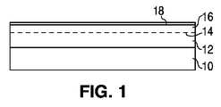
図1において、n型領域12、発光領域14、及びp型領域16を含むデバイス層は基板10の上で成長させる。基板は例えば、US 2008/0153192に記載されるサファイアのような成長基板上で成長させたテンプレートの1つ、US 2007/0072324に記載される複合基板であって例えばサファイアホスト、サファイア、SiC、又はSi基板に結合させたInGaNシード層であってもよい。
p型領域16は、発光領域14の上で成長させる。n型領域と同様に、p型領域は、異なる組成、厚さ、及びドーパント濃度(意図的にドープされていない層、又はn型層を含む)の複数の層を含んでもよい。
p接点18はp型領域16の頂上表面上に形成される。p接点18は反射層、例えば銀を含んでもよい。p接点18は、他の追加の層、例えばオーミック接触層及び、例えばチタン及び/又はタングステンを含む保護シートを含んでもよい。いくつかの態様において、接点間で生成される光は吸収され易いことから、p接点18は後に形成されるn接点と一致する領域から除去されて、p型及びn型接点の直接間の発光領域において光が生成されるのを防止する。抵抗性材料(図1に示されたものでない)のような電流を阻止する構造が、これらの領域内に形成されてもよい。
半導体構造がマウント26へ結合された後に、成長基板10は除去されてもよい。例えば、サファイア成長基板又は複合基板の一部であるサファイアホスト基板は、サファイア基板との境界面においてIII族窒化物又は他の層のレーザー溶融により除去されてもよい。他の技術、例えばエッチング又はグラインディングのような機械的な技術が基板の除去に適切であるように使用されてもよい。基板の一部、例えば複合基板のシード層又は非III族窒化物の成長基板上で成長した格子定数を拡張させるテンプレートの1以上の半導体層は、除去もされてもよいが、デバイス部分のまま残存してもよい。溝22の中の結合層24が基板を除去するのと同じ工程により除去されない場合、NiAuのような残存結合層の材料は、例えばウェットエッチングにより除去されてもよい。
いくつかの態様において、基板10の全て又は一部が除去された後、半導体構造は、例えば光電気化学(PEC)エッチングにより薄くされる。半導体構造の露出表面は、多くの場合n型領域12の表面であり、例えば粗面化されることにより又は光結晶の形成によりテクスチャー化されてもよい。
成長基板がエッチングにより除去される態様において、例えばシリコンの成長基板の場合において、溝22は図2及び3に示されるように成長基板が除去される前よりも除去された後エピタキシャル層内に形成されてもよい。これらの態様において、溝22は透明な導電性材料34が形成された後に形成されてもよい。
与えられたIII族窒化物材料において、Ω/squareで表されるシート抵抗は、厚さ及びドーピングの関数である。n型領域12のシート抵抗は、いくつかの態様においては90Ω/squareよりも大きく、及びいくつかの態様においては80Ω/squareよりも大きくてもよい。n型領域12及び透明な導電性材料24の組み合わせは、いくつかの態様においては70Ω/square未満及びいくつかの態様においては60Ω/square未満のシート抵抗を有していてもよい。対照的に、厚いGaNのn型領域を有する従来のIII族窒化物デバイスにおいて、n型領域のシート抵抗は約40Ω/squareである。
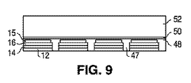
図6は複合基板10上で成長させたn型領域12、発光領域14、及びp型領域16を示す。複合基板10はホスト基板40、例えばサファイア;結合層42及び44、例えばそれぞれシリコンの窒化物及びシリコンの酸化物;及びシード層46、例えば8%以下のInN組成を有するInGaNを含む。シード層は、例えば米国出願番号12/236,853(参照により本明細書に組み込まれる)に記載されるような領域又は島状に形成されてもよい。シード層は、例えばいくつかの態様においては500Å〜2000Å厚及びいくつかの態様においては約1000Å層であってもよい。デバイス層12、14及び16は、半導体領域の間の溝47が維持されるよう、水平方向よりも垂直方向の成長に有利になるような条件下で成長させる。いくつかの態様において、n型領域12は0.2〜0.5μm厚のInGaN領域であり、発光領域14は約1000Å厚の多重量子井戸の活性領域であり、及びp型領域16は約1000Å厚のInGaNの層である。
図8において、図6のホスト基板40並びに結合層42及び44は、特別なホスト基板材料の除去に適切な技術により除去される。例えば、サファイアホストはレーザー溶融により除去されてもよい。
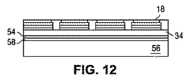
図10において、透明な導電性材料34が露出したn型領域12上に形成される。透明な導電性材料34は、例えばITOのような透明な導電性酸化物であってもよい。追加の結合層54、例えばシリコンの酸化物が透明な導電性材料34上に形成され、その後例えば化学機械研磨により研磨されてもよい。
図12において、残存している結合層、例えば結合層50及び結合層48が除去されてp接点の頂上表面が露出してもよい。
図13に示されるデバイスにおいて、光はそのデバイスから光学部材56を通って取り出される。1つのLEDが1つの領域又は複数の領域を含んでいてもよい。
Claims (10)
- n型領域及びp型領域の間に配置されたIII-V族発光層を含む半導体構造と、
前記n型領域と直接接触している、透明な導電性の非III族窒化物材料と、
前記透明な導電性の非III族窒化物材料と反対側の半導体構造の表面であるp型領域の表面上に配置された反射金属のp接点と、
前記n型領域に直接接触する、前記透明な導電性の非III族窒化物材料の表面を露出するように形成された少なくとも1つの開口部に配置された金属のn接点と、
を含み、
前記発光層と前記透明な導電性の非III族窒化物材料との間の半導体材料の総厚が、0.8μm以下であり、
前記半導体構造から取り出される光の大部分が前記透明な導電性の非III族窒化物材料を通って取り出される、
デバイス。 - 透明な導電性の非III族窒化物材料が酸化物である、請求項1に記載のデバイス。
- 前記p型領域の表面上に配置された反射金属の前記p接点及び透明な導電性の非III族窒化物材料の間の半導体材料は全てInGaNである、請求項1に記載のデバイス。
- 発光層及び透明な導電性の非III族窒化物材料の間の半導体材料の面内格子定数が3.186Åより大きい、請求項1に記載のデバイス。
- 透明な導電性の非III族窒化物材料に結合された光学部材をさらに含む請求項1に記載のデバイス。
- 透明な導電性の非III族窒化物材料に結合された発光セラミックをさらに含む請求項1に記載のデバイス。
- 透明な導電性の非III族窒化物材料に形成された溝に合わせた半導体材料に形成された溝をさらに含む請求項1に記載のデバイス。
- 発光層がIII族窒化物材料である、請求項1に記載のデバイス。
- n型領域が90Ω/squareよりも大きいシート抵抗を有し、並びにn型領域及び透明な導電性の非III族窒化物材料の組み合わせが70Ω/square未満のシート抵抗を有する、請求項1に記載のデバイス。
- n型領域が80Ω/squareよりも大きいシート抵抗を有し、並びにn型領域及び透明な導電性の非III族窒化物材料の組み合わせが60Ω/square未満のシート抵抗を有する、請求項1に記載のデバイス。
Applications Claiming Priority (3)
| Application Number | Priority Date | Filing Date | Title |
|---|---|---|---|
| US12/624,268 US8581229B2 (en) | 2009-11-23 | 2009-11-23 | III-V light emitting device with thin n-type region |
| US12/624,268 | 2009-11-23 | ||
| PCT/IB2010/055147 WO2011061664A1 (en) | 2009-11-23 | 2010-11-12 | Iii-v light emitting device with thin n-type region |
Publications (3)
| Publication Number | Publication Date |
|---|---|
| JP2013511853A JP2013511853A (ja) | 2013-04-04 |
| JP2013511853A5 JP2013511853A5 (ja) | 2013-12-26 |
| JP5674806B2 true JP5674806B2 (ja) | 2015-02-25 |
Family
ID=43502070
Family Applications (1)
| Application Number | Title | Priority Date | Filing Date |
|---|---|---|---|
| JP2012540516A Active JP5674806B2 (ja) | 2009-11-23 | 2010-11-12 | 薄いn型領域を有するIII−V族発光デバイス |
Country Status (7)
| Country | Link |
|---|---|
| US (2) | US8581229B2 (ja) |
| EP (1) | EP2504868B1 (ja) |
| JP (1) | JP5674806B2 (ja) |
| KR (2) | KR101762368B1 (ja) |
| CN (1) | CN102714255B (ja) |
| TW (1) | TWI523258B (ja) |
| WO (1) | WO2011061664A1 (ja) |
Families Citing this family (9)
| Publication number | Priority date | Publication date | Assignee | Title |
|---|---|---|---|---|
| DE102011012298A1 (de) * | 2010-12-28 | 2012-06-28 | Osram Opto Semiconductors Gmbh | Verbundsubstrat, Halbleiterchip mit Verbundsubstrat und Verfahren zur Herstellung von Verbundsubstraten und Halbleiterchips |
| KR20120099318A (ko) * | 2011-01-26 | 2012-09-10 | 엘지이노텍 주식회사 | 발광 소자 및 그 제조방법 |
| EP2748864B1 (en) * | 2011-08-26 | 2020-02-05 | Lumileds Holding B.V. | Method of processing a semiconductor structure |
| JP2014027092A (ja) * | 2012-07-26 | 2014-02-06 | Sharp Corp | 半導体発光素子 |
| CN104508815B (zh) | 2012-07-31 | 2018-02-13 | 索泰克公司 | 使用激光剥离过程制造半导体结构的方法和相关的半导体结构 |
| US9653647B2 (en) | 2013-06-14 | 2017-05-16 | Micron Technology, Inc. | Ultrathin solid state dies and methods of manufacturing the same |
| WO2015152817A1 (en) * | 2014-03-31 | 2015-10-08 | Nanyang Technological University | Methods of recycling substrates and carrier substrates |
| DE102016124646A1 (de) * | 2016-12-16 | 2018-06-21 | Osram Opto Semiconductors Gmbh | Verfahren zur Herstellung eines Halbleiterbauelements |
| CN111933765B (zh) * | 2020-07-03 | 2022-04-26 | 厦门士兰明镓化合物半导体有限公司 | 微型发光二极管及制作方法,微型led显示模块及制作方法 |
Family Cites Families (28)
| Publication number | Priority date | Publication date | Assignee | Title |
|---|---|---|---|---|
| JP3757544B2 (ja) * | 1997-05-21 | 2006-03-22 | 昭和電工株式会社 | Iii族窒化物半導体発光素子 |
| WO2002056394A1 (en) | 2001-01-09 | 2002-07-18 | Emcore Corporation | Electrode structures for p-type nitride semiconductores and mehtods of making same |
| JP3896027B2 (ja) * | 2002-04-17 | 2007-03-22 | シャープ株式会社 | 窒化物系半導体発光素子およびその製造方法 |
| TWI249148B (en) * | 2004-04-13 | 2006-02-11 | Epistar Corp | Light-emitting device array having binding layer |
| US7880182B2 (en) * | 2002-07-15 | 2011-02-01 | Epistar Corporation | Light-emitting element array |
| JP4295669B2 (ja) * | 2003-05-22 | 2009-07-15 | パナソニック株式会社 | 半導体素子の製造方法 |
| JP4135567B2 (ja) * | 2003-06-10 | 2008-08-20 | 松下電器産業株式会社 | キャップ取り外し装置 |
| US20050173724A1 (en) * | 2004-02-11 | 2005-08-11 | Heng Liu | Group III-nitride based LED having a transparent current spreading layer |
| JP2005268581A (ja) * | 2004-03-19 | 2005-09-29 | Matsushita Electric Ind Co Ltd | 窒化ガリウム系化合物半導体発光素子 |
| TWM255518U (en) * | 2004-04-23 | 2005-01-11 | Super Nova Optoelectronics Cor | Vertical electrode structure of Gallium Nitride based LED |
| US7361938B2 (en) * | 2004-06-03 | 2008-04-22 | Philips Lumileds Lighting Company Llc | Luminescent ceramic for a light emitting device |
| TWI299914B (en) * | 2004-07-12 | 2008-08-11 | Epistar Corp | Light emitting diode with transparent electrically conductive layer and omni directional reflector |
| US8334155B2 (en) * | 2005-09-27 | 2012-12-18 | Philips Lumileds Lighting Company Llc | Substrate for growing a III-V light emitting device |
| JP5232970B2 (ja) * | 2006-04-13 | 2013-07-10 | 豊田合成株式会社 | 半導体発光素子の製造方法及び半導体発光素子とそれを備えたランプ |
| JP2008053425A (ja) * | 2006-08-24 | 2008-03-06 | Matsushita Electric Ind Co Ltd | 半導体発光装置 |
| JP4929924B2 (ja) * | 2006-08-25 | 2012-05-09 | サンケン電気株式会社 | 半導体発光素子、その製造方法、及び複合半導体装置 |
| JP2008177525A (ja) * | 2006-12-20 | 2008-07-31 | Showa Denko Kk | Iii族窒化物半導体発光素子の製造方法、及びiii族窒化物半導体発光素子、並びにランプ |
| US7951693B2 (en) * | 2006-12-22 | 2011-05-31 | Philips Lumileds Lighting Company, Llc | III-nitride light emitting devices grown on templates to reduce strain |
| US8704254B2 (en) * | 2006-12-22 | 2014-04-22 | Philips Lumileds Lighting Company, Llc | Light emitting device including a filter |
| TWI331411B (en) * | 2006-12-29 | 2010-10-01 | Epistar Corp | High efficiency light-emitting diode and method for manufacturing the same |
| US7791096B2 (en) * | 2007-06-08 | 2010-09-07 | Koninklijke Philips Electronics N.V. | Mount for a semiconductor light emitting device |
| US20090050905A1 (en) * | 2007-08-20 | 2009-02-26 | Abu-Ageel Nayef M | Highly Efficient Light-Emitting Diode |
| US20090140279A1 (en) * | 2007-12-03 | 2009-06-04 | Goldeneye, Inc. | Substrate-free light emitting diode chip |
| KR101025948B1 (ko) * | 2007-12-21 | 2011-03-30 | 삼성엘이디 주식회사 | 질화물 반도체 발광소자 및 그 제조방법 |
| US7939839B2 (en) * | 2008-09-11 | 2011-05-10 | Bridgelux, Inc. | Series connected segmented LED |
| US9117944B2 (en) * | 2008-09-24 | 2015-08-25 | Koninklijke Philips N.V. | Semiconductor light emitting devices grown on composite substrates |
| US8089091B2 (en) * | 2009-06-18 | 2012-01-03 | Koninklijke Philips Electronics N.V. | Semiconductor light emitting device with a contact formed on a textured surface |
| US20100327300A1 (en) * | 2009-06-25 | 2010-12-30 | Koninklijke Philips Electronics N.V. | Contact for a semiconductor light emitting device |
-
2009
- 2009-11-23 US US12/624,268 patent/US8581229B2/en active Active
-
2010
- 2010-11-12 KR KR1020127016290A patent/KR101762368B1/ko active IP Right Grant
- 2010-11-12 EP EP10788136.9A patent/EP2504868B1/en active Active
- 2010-11-12 JP JP2012540516A patent/JP5674806B2/ja active Active
- 2010-11-12 KR KR1020177020575A patent/KR101905590B1/ko active IP Right Grant
- 2010-11-12 WO PCT/IB2010/055147 patent/WO2011061664A1/en active Application Filing
- 2010-11-12 CN CN201080062108.3A patent/CN102714255B/zh active Active
- 2010-11-23 TW TW099140450A patent/TWI523258B/zh active
-
2013
- 2013-10-09 US US14/049,282 patent/US8878160B2/en active Active
Also Published As
| Publication number | Publication date |
|---|---|
| US8581229B2 (en) | 2013-11-12 |
| EP2504868B1 (en) | 2018-05-16 |
| WO2011061664A1 (en) | 2011-05-26 |
| CN102714255B (zh) | 2015-10-21 |
| US8878160B2 (en) | 2014-11-04 |
| EP2504868A1 (en) | 2012-10-03 |
| TW201125161A (en) | 2011-07-16 |
| KR101905590B1 (ko) | 2018-10-10 |
| TWI523258B (zh) | 2016-02-21 |
| CN102714255A (zh) | 2012-10-03 |
| KR20120094502A (ko) | 2012-08-24 |
| KR101762368B1 (ko) | 2017-07-27 |
| US20110121332A1 (en) | 2011-05-26 |
| US20140034990A1 (en) | 2014-02-06 |
| KR20170098304A (ko) | 2017-08-29 |
| JP2013511853A (ja) | 2013-04-04 |
Similar Documents
| Publication | Publication Date | Title |
|---|---|---|
| JP5674806B2 (ja) | 薄いn型領域を有するIII−V族発光デバイス | |
| JP5441297B2 (ja) | Iii−v族発光デバイス | |
| KR101674228B1 (ko) | 복합 기판 상에 성장되는 반도체 발광 장치 | |
| KR101783796B1 (ko) | 복합 기판의 형성 및 복합 기판 상 ⅲ-ⅴ족 발광 장치 성장 방법 | |
| JP6419077B2 (ja) | 波長変換発光デバイス | |
| KR102071163B1 (ko) | 광 추출 구조체를 포함하는 ⅲ-ⅴ족 발광 장치 | |
| JP6535598B2 (ja) | フィルタ及び保護層を含む発光デバイス | |
| US20110177638A1 (en) | Semiconductor light emitting device with curvature control layer | |
| TW201332149A (zh) | 於半導體發光裝置上形成厚金屬層 | |
| KR101810711B1 (ko) | 반도체 소자를 성장시키기 위한 복합 성장 기판 |
Legal Events
| Date | Code | Title | Description |
|---|---|---|---|
| RD02 | Notification of acceptance of power of attorney |
Free format text: JAPANESE INTERMEDIATE CODE: A7422 Effective date: 20130711 |
|
| RD04 | Notification of resignation of power of attorney |
Free format text: JAPANESE INTERMEDIATE CODE: A7424 Effective date: 20130712 |
|
| A521 | Request for written amendment filed |
Free format text: JAPANESE INTERMEDIATE CODE: A523 Effective date: 20131108 |
|
| A621 | Written request for application examination |
Free format text: JAPANESE INTERMEDIATE CODE: A621 Effective date: 20131108 |
|
| A977 | Report on retrieval |
Free format text: JAPANESE INTERMEDIATE CODE: A971007 Effective date: 20140324 |
|
| A131 | Notification of reasons for refusal |
Free format text: JAPANESE INTERMEDIATE CODE: A131 Effective date: 20140408 |
|
| A521 | Request for written amendment filed |
Free format text: JAPANESE INTERMEDIATE CODE: A523 Effective date: 20140623 |
|
| TRDD | Decision of grant or rejection written | ||
| A01 | Written decision to grant a patent or to grant a registration (utility model) |
Free format text: JAPANESE INTERMEDIATE CODE: A01 Effective date: 20141126 |
|
| A61 | First payment of annual fees (during grant procedure) |
Free format text: JAPANESE INTERMEDIATE CODE: A61 Effective date: 20141222 |
|
| R150 | Certificate of patent or registration of utility model |
Ref document number: 5674806 Country of ref document: JP Free format text: JAPANESE INTERMEDIATE CODE: R150 |
|
| R250 | Receipt of annual fees |
Free format text: JAPANESE INTERMEDIATE CODE: R250 |
|
| R250 | Receipt of annual fees |
Free format text: JAPANESE INTERMEDIATE CODE: R250 |
|
| S111 | Request for change of ownership or part of ownership |
Free format text: JAPANESE INTERMEDIATE CODE: R313113 |
|
| S533 | Written request for registration of change of name |
Free format text: JAPANESE INTERMEDIATE CODE: R313533 |
|
| R350 | Written notification of registration of transfer |
Free format text: JAPANESE INTERMEDIATE CODE: R350 |
|
| R250 | Receipt of annual fees |
Free format text: JAPANESE INTERMEDIATE CODE: R250 |
|
| R250 | Receipt of annual fees |
Free format text: JAPANESE INTERMEDIATE CODE: R250 |
|
| R250 | Receipt of annual fees |
Free format text: JAPANESE INTERMEDIATE CODE: R250 |
|
| R250 | Receipt of annual fees |
Free format text: JAPANESE INTERMEDIATE CODE: R250 |
|
| R250 | Receipt of annual fees |
Free format text: JAPANESE INTERMEDIATE CODE: R250 |