EP2504868B1 - Iii-v light emitting device with a thin n-type region - Google Patents
Iii-v light emitting device with a thin n-type region Download PDFInfo
- Publication number
- EP2504868B1 EP2504868B1 EP10788136.9A EP10788136A EP2504868B1 EP 2504868 B1 EP2504868 B1 EP 2504868B1 EP 10788136 A EP10788136 A EP 10788136A EP 2504868 B1 EP2504868 B1 EP 2504868B1
- Authority
- EP
- European Patent Office
- Prior art keywords
- iii
- type region
- transparent
- light emitting
- nitride material
- Prior art date
- Legal status (The legal status is an assumption and is not a legal conclusion. Google has not performed a legal analysis and makes no representation as to the accuracy of the status listed.)
- Active
Links
- 239000000463 material Substances 0.000 claims description 61
- 239000004065 semiconductor Substances 0.000 claims description 33
- 230000003287 optical effect Effects 0.000 claims description 12
- 239000000919 ceramic Substances 0.000 claims description 10
- 229910052751 metal Inorganic materials 0.000 claims description 8
- 239000002184 metal Substances 0.000 claims description 8
- 239000000758 substrate Substances 0.000 description 59
- 239000004020 conductor Substances 0.000 description 24
- 229910052594 sapphire Inorganic materials 0.000 description 14
- 239000010980 sapphire Substances 0.000 description 14
- 239000002131 composite material Substances 0.000 description 11
- 229910052710 silicon Inorganic materials 0.000 description 10
- XUIMIQQOPSSXEZ-UHFFFAOYSA-N Silicon Chemical compound [Si] XUIMIQQOPSSXEZ-UHFFFAOYSA-N 0.000 description 8
- 238000000034 method Methods 0.000 description 8
- 239000000203 mixture Substances 0.000 description 8
- 239000010703 silicon Substances 0.000 description 8
- 238000005530 etching Methods 0.000 description 5
- 239000000126 substance Substances 0.000 description 5
- 238000003892 spreading Methods 0.000 description 4
- 230000007480 spreading Effects 0.000 description 4
- 238000005336 cracking Methods 0.000 description 3
- 239000002019 doping agent Substances 0.000 description 3
- 230000008018 melting Effects 0.000 description 3
- 238000002844 melting Methods 0.000 description 3
- 150000004767 nitrides Chemical class 0.000 description 3
- 238000005498 polishing Methods 0.000 description 3
- HBMJWWWQQXIZIP-UHFFFAOYSA-N silicon carbide Chemical compound [Si+]#[C-] HBMJWWWQQXIZIP-UHFFFAOYSA-N 0.000 description 3
- 229910010271 silicon carbide Inorganic materials 0.000 description 3
- IJGRMHOSHXDMSA-UHFFFAOYSA-N Atomic nitrogen Chemical compound N#N IJGRMHOSHXDMSA-UHFFFAOYSA-N 0.000 description 2
- 229910052782 aluminium Inorganic materials 0.000 description 2
- 230000004888 barrier function Effects 0.000 description 2
- 229910052733 gallium Inorganic materials 0.000 description 2
- 229910052732 germanium Inorganic materials 0.000 description 2
- 229910052738 indium Inorganic materials 0.000 description 2
- 229910052451 lead zirconate titanate Inorganic materials 0.000 description 2
- 229920001296 polysiloxane Polymers 0.000 description 2
- 239000000843 powder Substances 0.000 description 2
- 229910052719 titanium Inorganic materials 0.000 description 2
- 239000010936 titanium Substances 0.000 description 2
- 229910052721 tungsten Inorganic materials 0.000 description 2
- 239000004593 Epoxy Substances 0.000 description 1
- GYHNNYVSQQEPJS-UHFFFAOYSA-N Gallium Chemical compound [Ga] GYHNNYVSQQEPJS-UHFFFAOYSA-N 0.000 description 1
- 229910052779 Neodymium Inorganic materials 0.000 description 1
- OAICVXFJPJFONN-UHFFFAOYSA-N Phosphorus Chemical compound [P] OAICVXFJPJFONN-UHFFFAOYSA-N 0.000 description 1
- VYPSYNLAJGMNEJ-UHFFFAOYSA-N Silicium dioxide Chemical compound O=[Si]=O VYPSYNLAJGMNEJ-UHFFFAOYSA-N 0.000 description 1
- RTAQQCXQSZGOHL-UHFFFAOYSA-N Titanium Chemical compound [Ti] RTAQQCXQSZGOHL-UHFFFAOYSA-N 0.000 description 1
- XAGFODPZIPBFFR-UHFFFAOYSA-N aluminium Chemical compound [Al] XAGFODPZIPBFFR-UHFFFAOYSA-N 0.000 description 1
- PNEYBMLMFCGWSK-UHFFFAOYSA-N aluminium oxide Inorganic materials [O-2].[O-2].[O-2].[Al+3].[Al+3] PNEYBMLMFCGWSK-UHFFFAOYSA-N 0.000 description 1
- 229910052787 antimony Inorganic materials 0.000 description 1
- 229910002056 binary alloy Inorganic materials 0.000 description 1
- 230000015572 biosynthetic process Effects 0.000 description 1
- 229910052797 bismuth Inorganic materials 0.000 description 1
- 230000000903 blocking effect Effects 0.000 description 1
- 229910052796 boron Inorganic materials 0.000 description 1
- 229910052791 calcium Inorganic materials 0.000 description 1
- 238000005229 chemical vapour deposition Methods 0.000 description 1
- 230000006835 compression Effects 0.000 description 1
- 238000007906 compression Methods 0.000 description 1
- 229910052593 corundum Inorganic materials 0.000 description 1
- 239000013078 crystal Substances 0.000 description 1
- 238000013461 design Methods 0.000 description 1
- 239000003989 dielectric material Substances 0.000 description 1
- 239000000975 dye Substances 0.000 description 1
- 238000005566 electron beam evaporation Methods 0.000 description 1
- 238000001652 electrophoretic deposition Methods 0.000 description 1
- 230000002349 favourable effect Effects 0.000 description 1
- 150000002222 fluorine compounds Chemical class 0.000 description 1
- 230000006870 function Effects 0.000 description 1
- 239000011521 glass Substances 0.000 description 1
- PCHJSUWPFVWCPO-UHFFFAOYSA-N gold Chemical compound [Au] PCHJSUWPFVWCPO-UHFFFAOYSA-N 0.000 description 1
- 229910052737 gold Inorganic materials 0.000 description 1
- 239000010931 gold Substances 0.000 description 1
- 238000000227 grinding Methods 0.000 description 1
- 229910052735 hafnium Inorganic materials 0.000 description 1
- 238000010348 incorporation Methods 0.000 description 1
- APFVFJFRJDLVQX-UHFFFAOYSA-N indium atom Chemical compound [In] APFVFJFRJDLVQX-UHFFFAOYSA-N 0.000 description 1
- 229910003437 indium oxide Inorganic materials 0.000 description 1
- PJXISJQVUVHSOJ-UHFFFAOYSA-N indium(iii) oxide Chemical compound [O-2].[O-2].[O-2].[In+3].[In+3] PJXISJQVUVHSOJ-UHFFFAOYSA-N 0.000 description 1
- AMGQUBHHOARCQH-UHFFFAOYSA-N indium;oxotin Chemical compound [In].[Sn]=O AMGQUBHHOARCQH-UHFFFAOYSA-N 0.000 description 1
- 229910010272 inorganic material Inorganic materials 0.000 description 1
- 239000011147 inorganic material Substances 0.000 description 1
- 229910052745 lead Inorganic materials 0.000 description 1
- HFGPZNIAWCZYJU-UHFFFAOYSA-N lead zirconate titanate Chemical compound [O-2].[O-2].[O-2].[O-2].[O-2].[Ti+4].[Zr+4].[Pb+2] HFGPZNIAWCZYJU-UHFFFAOYSA-N 0.000 description 1
- 229910052749 magnesium Inorganic materials 0.000 description 1
- 238000004519 manufacturing process Methods 0.000 description 1
- 150000001247 metal acetylides Chemical class 0.000 description 1
- 150000002739 metals Chemical class 0.000 description 1
- 238000012986 modification Methods 0.000 description 1
- 230000004048 modification Effects 0.000 description 1
- 229910003465 moissanite Inorganic materials 0.000 description 1
- 238000001451 molecular beam epitaxy Methods 0.000 description 1
- 229910052759 nickel Inorganic materials 0.000 description 1
- 229910052757 nitrogen Inorganic materials 0.000 description 1
- 230000006911 nucleation Effects 0.000 description 1
- 238000010899 nucleation Methods 0.000 description 1
- 239000011368 organic material Substances 0.000 description 1
- TWNQGVIAIRXVLR-UHFFFAOYSA-N oxo(oxoalumanyloxy)alumane Chemical compound O=[Al]O[Al]=O TWNQGVIAIRXVLR-UHFFFAOYSA-N 0.000 description 1
- 238000000059 patterning Methods 0.000 description 1
- 229910052698 phosphorus Inorganic materials 0.000 description 1
- 239000004038 photonic crystal Substances 0.000 description 1
- 238000000623 plasma-assisted chemical vapour deposition Methods 0.000 description 1
- 229910052700 potassium Inorganic materials 0.000 description 1
- 238000002360 preparation method Methods 0.000 description 1
- 230000008569 process Effects 0.000 description 1
- 238000012545 processing Methods 0.000 description 1
- 229910002059 quaternary alloy Inorganic materials 0.000 description 1
- 238000007788 roughening Methods 0.000 description 1
- 238000007650 screen-printing Methods 0.000 description 1
- 238000004062 sedimentation Methods 0.000 description 1
- 229910052814 silicon oxide Inorganic materials 0.000 description 1
- 229910052709 silver Inorganic materials 0.000 description 1
- 239000004332 silver Substances 0.000 description 1
- 229910000679 solder Inorganic materials 0.000 description 1
- 238000009987 spinning Methods 0.000 description 1
- 238000004544 sputter deposition Methods 0.000 description 1
- 229910052715 tantalum Inorganic materials 0.000 description 1
- 229910002058 ternary alloy Inorganic materials 0.000 description 1
- 238000012360 testing method Methods 0.000 description 1
- -1 thickness Substances 0.000 description 1
- 229910052718 tin Inorganic materials 0.000 description 1
- 239000012780 transparent material Substances 0.000 description 1
- WFKWXMTUELFFGS-UHFFFAOYSA-N tungsten Chemical compound [W] WFKWXMTUELFFGS-UHFFFAOYSA-N 0.000 description 1
- 239000010937 tungsten Substances 0.000 description 1
- 238000001429 visible spectrum Methods 0.000 description 1
- 238000001039 wet etching Methods 0.000 description 1
- 229910001845 yogo sapphire Inorganic materials 0.000 description 1
- 229910052727 yttrium Inorganic materials 0.000 description 1
- 229910052725 zinc Inorganic materials 0.000 description 1
- 229910052726 zirconium Inorganic materials 0.000 description 1
Images


Classifications
-
- H—ELECTRICITY
- H01—ELECTRIC ELEMENTS
- H01L—SEMICONDUCTOR DEVICES NOT COVERED BY CLASS H10
- H01L33/00—Semiconductor devices having potential barriers specially adapted for light emission; Processes or apparatus specially adapted for the manufacture or treatment thereof or of parts thereof; Details thereof
- H01L33/36—Semiconductor devices having potential barriers specially adapted for light emission; Processes or apparatus specially adapted for the manufacture or treatment thereof or of parts thereof; Details thereof characterised by the electrodes
- H01L33/40—Materials therefor
- H01L33/42—Transparent materials
-
- H—ELECTRICITY
- H01—ELECTRIC ELEMENTS
- H01L—SEMICONDUCTOR DEVICES NOT COVERED BY CLASS H10
- H01L33/00—Semiconductor devices having potential barriers specially adapted for light emission; Processes or apparatus specially adapted for the manufacture or treatment thereof or of parts thereof; Details thereof
- H01L33/005—Processes
- H01L33/0093—Wafer bonding; Removal of the growth substrate
-
- H—ELECTRICITY
- H01—ELECTRIC ELEMENTS
- H01L—SEMICONDUCTOR DEVICES NOT COVERED BY CLASS H10
- H01L33/00—Semiconductor devices having potential barriers specially adapted for light emission; Processes or apparatus specially adapted for the manufacture or treatment thereof or of parts thereof; Details thereof
- H01L33/02—Semiconductor devices having potential barriers specially adapted for light emission; Processes or apparatus specially adapted for the manufacture or treatment thereof or of parts thereof; Details thereof characterised by the semiconductor bodies
- H01L33/10—Semiconductor devices having potential barriers specially adapted for light emission; Processes or apparatus specially adapted for the manufacture or treatment thereof or of parts thereof; Details thereof characterised by the semiconductor bodies with a light reflecting structure, e.g. semiconductor Bragg reflector
-
- H—ELECTRICITY
- H01—ELECTRIC ELEMENTS
- H01L—SEMICONDUCTOR DEVICES NOT COVERED BY CLASS H10
- H01L33/00—Semiconductor devices having potential barriers specially adapted for light emission; Processes or apparatus specially adapted for the manufacture or treatment thereof or of parts thereof; Details thereof
- H01L33/02—Semiconductor devices having potential barriers specially adapted for light emission; Processes or apparatus specially adapted for the manufacture or treatment thereof or of parts thereof; Details thereof characterised by the semiconductor bodies
- H01L33/26—Materials of the light emitting region
- H01L33/30—Materials of the light emitting region containing only elements of Group III and Group V of the Periodic Table
- H01L33/32—Materials of the light emitting region containing only elements of Group III and Group V of the Periodic Table containing nitrogen
-
- H—ELECTRICITY
- H01—ELECTRIC ELEMENTS
- H01L—SEMICONDUCTOR DEVICES NOT COVERED BY CLASS H10
- H01L2933/00—Details relating to devices covered by the group H01L33/00 but not provided for in its subgroups
- H01L2933/0008—Processes
- H01L2933/0016—Processes relating to electrodes
-
- H—ELECTRICITY
- H01—ELECTRIC ELEMENTS
- H01L—SEMICONDUCTOR DEVICES NOT COVERED BY CLASS H10
- H01L33/00—Semiconductor devices having potential barriers specially adapted for light emission; Processes or apparatus specially adapted for the manufacture or treatment thereof or of parts thereof; Details thereof
- H01L33/48—Semiconductor devices having potential barriers specially adapted for light emission; Processes or apparatus specially adapted for the manufacture or treatment thereof or of parts thereof; Details thereof characterised by the semiconductor body packages
- H01L33/50—Wavelength conversion elements
- H01L33/505—Wavelength conversion elements characterised by the shape, e.g. plate or foil
Definitions
- LEDs light emitting diodes
- RCLEDs resonant cavity light emitting diodes
- VCSELs vertical cavity laser diodes
- edge emitting lasers are among the most efficient light sources currently available.
- Materials systems currently of interest in the manufacture of high-brightness light emitting devices capable of operation across the visible spectrum include Group III-V semiconductors, particularly binary, ternary, and quaternary alloys of gallium, aluminum, indium, and nitrogen, also referred to as III-nitride materials.
- III-nitride light emitting devices are fabricated by epitaxially growing a stack of semiconductor layers of different compositions and dopant concentrations on a sapphire, silicon carbide, III-nitride, or other suitable substrate by metal-organic chemical vapor deposition (MOCVD), molecular beam epitaxy (MBE), or other epitaxial techniques.
- MOCVD metal-organic chemical vapor deposition
- MBE molecular beam epitaxy
- the stack often includes one or more n-type layers doped with, for example, Si, formed over the substrate, one or more light emitting layers in an active region formed over the n-type layer or layers, and one or more p-type layers doped with, for example, Mg, formed over the active region. Electrical contacts are formed on the n- and p-type regions.
- III-nitride devices are often grown on sapphire (Al 2 O 3 ), SiC, or Si substrates.
- Such non-native substrates have different lattice constants than the bulk lattice constants of the III-nitride device layers grown on the substrate, different thermal expansion coefficients, and different chemical and structural properties than the device layers, resulting in strain in the device layers, and chemical and structural mismatch between the device layers and the substrates.
- Growth of thick layers can reduce the output of the device, and require extra source material, which can increase the cost of a device. If the device layers are grown overly thick, the strain may be relieved by cracking, which can negatively impact the device performance.
- the first structure grown on the substrate is generally a GaN template layer with an in-plane a-lattice constant of about 3.189 ⁇ or less.
- the GaN template serves as a lattice constant template for the light emitting region in that it sets the lattice constant for all of the strained layers grown above the template layer, including the InGaN light emitting layer. Since the bulk lattice constant of InGaN is larger than the in-plane lattice constant of the conventional GaN template, the light emitting layer is compressively strained when grown over a conventional GaN template.
- a light emitting layer configured to emit light of about 450 nm may have a composition In 0.16 Ga 0.84 N, a composition with a bulk lattice constant of 3.242 ⁇ , as compared to the lattice constant of GaN, 3.189 ⁇ .
- the InN composition in the light emitting layer increases, as in devices designed to emit light at longer wavelengths, the compressive strain in the light emitting layer also increases.
- US 2008/0153192 titled "III-nitride light emitting devices grown on templates to reduce strain” , teaches growing the device layers including the light emitting layer of a III-nitride device over a template designed to reduce strain in the device, in particular in the light emitting layer.
- the template is grown on a conventional substrate such as sapphire.
- US 2007/0072324 titled “Substrate for growing a III-V light emitting device” teaches growing a III-nitride device over a composite substrate, which includes a host substrate, a seed layer, and a bonding layer that bonds the host to the seed layer.
- the host substrate provides mechanical support to the composite substrate and to the semiconductor device layers grown over the composite substrate.
- the seed layer is generally a single crystal material that is a reasonably close lattice-match to the device layers. With such a substrate, it is possible to increase the lattice constant beyond GaN, in which case the device layers grown on these templates generally contain In. Incorporation of In is not energetically favorable and growth of InGaN is slow. Thick InGaN layers are therefore not commercially feasible.
- US20050236632 A discloses a semiconductor device.
- a device in embodiments of the invention, includes a semiconductor structure comprising a III-nitride light emitting layer disposed between an n-type region and a p-type region.
- a transparent, conductive non-III-nitride material is disposed in direct contact with the n-type region.
- a total thickness of semiconductor material between the light emitting layer and the transparent, conductive non-III-nitride material is less than 0.8 ⁇ m.
- a p-contact is formed on the surface of the last p-type layer grown in the device, then a mesa is etched to expose a portion of the n-type region on which an n-contact is formed.
- the p-contact typically covers a much larger area than the n-contact, since current spreads more readily through n-type III-nitride material.
- the n-contact is typically formed on an n-type GaN layer.
- the n-type GaN layer must be thick enough and conductive enough to provide a low sheet resistance, for example less than 20 ⁇ /square, in a conventional III-nitride flip-chip device.
- a given layer has a bulk lattice constant a bulk corresponding to a lattice constant of free standing material of the same composition as that layer, and an in-plane lattice constant a in-plane corresponding to a lattice constant of that layer as grown in an actual device structure.
- the in-plane lattice constant set by the template is generally larger than the bulk lattice constant of GaN. As a result, GaN grown over such templates is in tension.
- InGaN which has a larger bulk lattice constant than GaN, can be grown over a reduced strain template in compression, or under less tension than GaN, and is thus often used as the n-type contact layer of a reduced strain device, instead of GaN.
- Growing an InGaN layer thick enough to serve as the n-contact layer in a device design that requires current to spread from the n-contact is prohibitively time-consuming and therefore expensive.
- Such a current spreading InGaN layer may be, for example, at least 2 ⁇ m thick.
- the contacts on a reduced strain III-nitride device are formed and arranged such that current spreading in a thick n-type region is not required.
- the n-type region may therefore be made thinner than in a device where current spreads through the n-type region.
- Figs. 1-5 illustrate forming a vertical device with a thin n-type region.
- n-type region 12 a light emitting region 14, and a p-type region 16 are grown over a substrate 10.
- the substrate may be, for example, one of the templates grown over a growth substrate such as sapphire as described in US 2008/0153192 , a composite substrate as described in US 2007/0072324 , such as, for example, an InGaN seed layer bonded to a sapphire host, or a sapphire, SiC, or Si substrate.
- the n-type region 12 may include multiple layers of different compositions and dopant concentration including, for example, preparation layers such as buffer layers or nucleation layers, which may be n-type or not intentionally doped, release layers designed to facilitate later release of the composite substrate or thinning of the semiconductor structure after substrate removal, and n- or even p-type device layers designed for particular optical or electrical properties desirable for the light emitting region to efficiently emit light.
- the n-type region is less than 0.8 ⁇ m thick. In some embodiments, the n-type region is less than 0.5 microns thick.
- the n-type region includes at least one InGaN layer. In some embodiments, the n-type region includes only InGaN.
- the n-type region has an in-plane lattice constant larger than the in-plane lattice constant of GaN grown on sapphire, or the n-type region has an in-plane lattice constant larger than 3.186 ⁇ .
- a light emitting or active region 14 is grown over the n-type region 12.
- suitable light emitting regions include a single thick or thin light emitting layer, or a multiple quantum well light emitting region including multiple thin or thick quantum well light emitting layers separated by barrier layers.
- a multiple quantum well light emitting region may include multiple light emitting layers, each with a thickness of 25 ⁇ or less, separated by barriers, each with a thickness of 100 ⁇ or less. In some embodiments, the thickness of each of the light emitting layers in the device is thicker than 50 ⁇ .
- a p-type region 16 is grown over the light emitting region 14. Like the n-type region, the p-type region may include multiple layers of different composition, thickness, and dopant concentration, including layers that are not intentionally doped, or n-type layers.
- a p-contact 18 is formed on the top surface of p-type region 16.
- P-contact 18 may include a reflective layer, such as silver.
- P-contact 18 may include other optional layers, such as an ohmic contact layer and a guard sheet including, for example, titanium and/or tungsten.
- p-contact 18 is removed from areas that are aligned with later-formed n-contacts, to prevent light from being generated in the light emitting region directly between the p- and n-contacts, since light generated between the contacts is likely to be absorbed.
- a current blocking structure such as a resistive material (not shown in Fig. 1 ), may be formed in these areas.
- trenches 22 are formed in the device.
- the trenches extend through the entire thickness of the III-nitride material, down to a non-III-nitride layer of substrate 10.
- an optional bonding layer 20 is disposed on the surface of p-contact 18.
- Bonding layer 24 may also be disposed in trenches 22.
- Bonding layer 20 and 24 may be, for example, a metal such as NiAu.
- Trenches 22 may be, for example, between 10-30 ⁇ m wide.
- trenches 22 form the boundaries of individual LEDs on a wafer of LEDs and are spaced in accordance with the desired die size, for example between 0.2 and 2 mm apart, often between 0.5 and 1 mm apart.
- Trenches 22 may limit damage caused by laser melting to remove all or part of substrate 10, as described below in reference to Fig. 3 .
- the device is bonded to a mount 26.
- An optional bonding layer 28 may be formed on mount 26.
- the semiconductor structure may be bonded to mount 26 via one or more bonding layers 20 and 28.
- Mount 26 may be, for example, Si, Ge, metal, or ceramic.
- Bonding layer 28 may be, for example, a metal such as NiAu.
- growth substrate 10 may be removed.
- a sapphire growth substrate or a sapphire host substrate that is part of a composite substrate may be removed by laser melting of a III-nitride or other layer at an interface with the sapphire substrate.
- Other techniques, such as etching or mechanical techniques such as grinding may be used as appropriate to the substrate being removed.
- Parts of the substrate such as, for example, the seed layer of a composite substrate or one or more semiconductor layers of a lattice-constant expanding template grown on a non-III-nitride growth substrate, may remain a part of the device, though they may also be removed.
- residual bonding layer material such as NiAu may be removed by, for example, wet etching.
- the semiconductor structure after removing all or part of substrate 10, the semiconductor structure is thinned, for example by photoelectrochemical (PEC) etching.
- PEC photoelectrochemical
- the exposed surface of the semiconductor structure often a surface of n-type region 12, may be textured, for example by roughening or by forming a photonic crystal.
- trenches 22 are partially or completely filled with a dielectric material, such as, for example, a nitride of silicon formed by plasma-enhanced chemical vapor deposition.
- a dielectric layer may also be formed over the surface of n-type region 12 exposed by removing substrate 10, then patterned such that the dielectric remains only in regions 32 overlying trenches 22.
- a transparent, conductive material 34 is disposed on the exposed surface of n-type region 12.
- transparent conductive material 34 is an oxide such as indium tin oxide (ITO).
- Transparent conductive material 34 may be deposited by, for example, electron beam evaporation, sputtering, spinning on, or sedimentation.
- the thickness of transparent conductive material 34 may be, for example, 0.5 to 1.5 ⁇ m, depending upon the thickness and doping of the n-type device layer, and the stoichiometry of the transparent conductive material.
- a thicker transparent conductive material layer may be formed on an n-type region that is thin or not highly doped, or if the transparent conductive material is not highly conductive.
- ITO indium oxide
- AZO aluminum-doped ZnO
- MZO magnesium-doped ZnO
- GZO gallium-doped ZnO
- AMZO aluminum-doped MZO
- ZIO ZnO-doped indium oxide
- GMZO gallium-doped MZO
- Transparent, conductive material 34 is formed thick enough to spread current in n-type region 12, but thin enough that it does not substantially absorb light emitted by the light emitting region.
- Trenches 36 which align with oxide regions 32, are formed in transparent conductive material 34 by conventional patterning steps.
- Metal n-contacts 38 are formed on transparent, conductive material 34.
- Trenches 36 and 22 electrically isolate adjacent regions of semiconductor material and transparent conductive material 34, which permits testing of individual regions before a wafer of individual regions is diced.
- trenches 22 may be formed in the epitaxial layers after the growth substrate is removed, rather than before, as illustrated in Figs. 2 and 3 . In these embodiments, trenches 22 may be formed after transparent, conductive material 34 is formed.
- Mount 26 and any bonding layers between mount 26 and p-contact 18 may be conductive, such that current is supplied to p-contact 18 through mount 26.
- a total thickness of the semiconductor material between light emitting region 14 and transparent conductive material 34 may be no more than 0.8 ⁇ m thick in some embodiments, and no more than 0.5 ⁇ m thick in some embodiments.
- the entire semiconductor structure between the transparent conductive material 34 and p-contact 18 is InGaN.
- the sheet resistance is a function of the thickness and doping.
- the sheet resistance of the n-type region 12 may be greater than 90 ⁇ /square in some embodiments and greater than 80 ⁇ /square in some embodiments.
- the combination of the n-type region 12 and the transparent, conductive material 24 may have a sheet resistance of less than 70 ⁇ /square in some embodiments and less than 60 ⁇ /square in some embodiments.
- the sheet resistance of the n-type region is about 40 ⁇ /square.
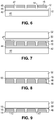
- Figs. 6-12 illustrate forming a device with a thin n-type region bonded to an optical element such as a luminescent ceramic. Materials and processing steps described in Figs. 6-12 may be the same as described above in Figs. 1-5 , and vice versa.
- Fig. 6 illustrates an n-type region 12, light emitting region 14, and p-type region 16 grown over a composite substrate 10.
- the composite substrate 10 includes a host substrate 40, such as, for example, sapphire; bonding layers 42 and 44, such as, for example, a nitride of silicon and an oxide of silicon, respectively; and a seed layer 46, such as, for example, InGaN with an InN composition of not more than 8%.
- the seed layer may be formed in regions or islands as described in, for example, US Application No. 12/236853 .
- the seed layer may be, for example, between 500 ⁇ and 2000 ⁇ thick in some embodiments and about 1000 ⁇ thick in some embodiments.
- n-type region 12 is an InGaN region between 0.2 and 0.5 microns thick
- light emitting region 14 is a multi-quantum-well active region about 1000 ⁇ thick
- p-type region 16 is a layer of InGaN about 1000 ⁇ thick.
- a p-contact 18 is formed over the p-type region 16, then patterned to remove the p-contact material disposed on the sidewalls of the regions of semiconductor material. Some p-contact material may remain in the bottom of trenches 47 between regions of semiconductor material. In some embodiments, poor quality semiconductor material on the sidewalls of the regions is removed at the same time.
- a bonding material 48 such as an oxide of silicon is disposed over the p-contact 18 and in the trenches 47 between regions of semiconductor material. The bonding material 48 may be optionally polished by, for example, chemical mechanical polishing.
- the semiconductor structure is bonded to an intermediate substrate 52 which may be, for example, sapphire, or any other suitable substrate with a coefficient of thermal expansion that is a reasonably close match to host 40.
- An optional bonding layer 50 which may be, for example, an oxide of silicon, may be formed on intermediate substrate 52.
- the host substrate 40 and bonding layers 42 and 44 of Fig. 6 are removed by a technique suitable for removing the particular host substrate material.
- a sapphire host may be removed by laser melting.
- the seed layer 46 is removed in Fig. 9 , by a technique suitable for removing the particular seed layer material.
- a technique suitable for removing the particular seed layer material For example, an InGaN or other III-nitride seed layer may be removed by PEC etching or chemical mechanical polishing (CMP).
- CMP chemical mechanical polishing
- the semiconductor structure may optionally be thinned, and the exposed surface may optionally be textured. Any p-contact material in the trenches 47 between islands of semiconductor material may also be removed.
- a transparent, conductive material 34 is formed on the exposed n-type region 12.
- the transparent conductive material 34 may be, for example, a transparent conductive oxide such as ITO.
- An optional bonding layer 54 such as, for example, an oxide of silicon may be formed on transparent, conductive material 34, then optionally polished by, for example, chemical mechanical polishing.
- the transparent, conductive material 34 is bonded to an optical element 56.
- An optional bonding layer 58 may be formed on optical element 56.
- the optical element may be, for example, a lens or a luminescent ceramic, also referred to as a ceramic phosphor.
- Luminescent ceramics may be phosphors formed into a ceramic. The luminescent ceramic absorbs light of a wavelength emitted by the light emitting region and emits light of a different wavelength. Luminescent ceramics are described in more detail in US Patent 7,361,938 , which is incorporated herein by reference.
- intermediate substrate 52 may be removed by a technique suitable to the substrate material. For example, a sapphire intermediate substrate may be removed by laser lift off.
- Bonding layers 48, 50, 54, and 58, shown in Figs. 7 , 10, and 11 may be, for example, an organic material such as silicone or an inorganic material such as silicon oxide. All of the bonding layers need not be the same material. In some embodiments, both bonding layers that form a bond are oxides of silicon. Oxide-oxide bonding may be employed to join either planar or nonplanar surfaces. To form an oxide-oxide bond, pressure is applied between the two structures. Heat may also be applied.
- a single LED may include a single region or multiple regions.
- the LED die is positioned on a mount.
- a bond head is positioned on the top surface of the LED die, for example on the top surface of the optical element 56.
- the bond head is connected to an ultrasonic transducer.
- the ultrasonic transducer may be, for example, a stack of lead zirconate titanate (PZT) layers.
- PZT lead zirconate titanate
- the vibration causes atoms in the metal lattice of a structure on the LED, such as the n- and p-contacts or interconnects formed on the n- and p-contacts, to interdiffuse with a structure on the mount, resulting in a metallurgically continuous joint.
- Heat and/or pressure may be added during bonding.
- One or more wavelength converting materials may be disposed over transparent conductive layer 34 of Fig. 5 or over the optical element 56 of Fig. 13 .
- the wavelength converting material(s) may be, for example, one or more powder phosphors disposed in a transparent material such as silicone or epoxy and deposited on the LED by screen printing or stenciling, one or more powder phosphors formed by electrophoretic deposition, or one or more ceramic phosphors glued or bonded to the LED, one or more dyes, or any combination of the above-described wavelength converting layers.
- the wavelength converting materials may be formed such that a portion of light emitted by the light emitting region is unconverted by the wavelength converting material. In some examples, the unconverted light is blue and the converted light is yellow, green, and/or red, such that the combination of unconverted and converted light emitted from the device appears white.
- polarizers, dichroic filters or other optics known in the art are formed over the transparent conductive layer 34 of Fig. 5 or over the optical element 56 of Fig. 13 .
- a thick n-type region for example, with a thickness of at least two microns, is not required, since current is spread through a non-III-nitride transparent conductive material such as a transparent conductive oxide. Since transparent conductive oxides are generally not as transparent as III-nitride materials, in a device where the transparent, conductive non-III-nitride material is not needed for current spreading, such as in a device with a thick n-type region, including the transparent conductive non-III-nitride material may reduce the light output of the device.
Landscapes
- Engineering & Computer Science (AREA)
- Microelectronics & Electronic Packaging (AREA)
- Manufacturing & Machinery (AREA)
- Computer Hardware Design (AREA)
- Power Engineering (AREA)
- Led Devices (AREA)
- Led Device Packages (AREA)
Applications Claiming Priority (2)
| Application Number | Priority Date | Filing Date | Title |
|---|---|---|---|
| US12/624,268 US8581229B2 (en) | 2009-11-23 | 2009-11-23 | III-V light emitting device with thin n-type region |
| PCT/IB2010/055147 WO2011061664A1 (en) | 2009-11-23 | 2010-11-12 | Iii-v light emitting device with thin n-type region |
Publications (2)
| Publication Number | Publication Date |
|---|---|
| EP2504868A1 EP2504868A1 (en) | 2012-10-03 |
| EP2504868B1 true EP2504868B1 (en) | 2018-05-16 |
Family
ID=43502070
Family Applications (1)
| Application Number | Title | Priority Date | Filing Date |
|---|---|---|---|
| EP10788136.9A Active EP2504868B1 (en) | 2009-11-23 | 2010-11-12 | Iii-v light emitting device with a thin n-type region |
Country Status (7)
| Country | Link |
|---|---|
| US (2) | US8581229B2 (ja) |
| EP (1) | EP2504868B1 (ja) |
| JP (1) | JP5674806B2 (ja) |
| KR (2) | KR101762368B1 (ja) |
| CN (1) | CN102714255B (ja) |
| TW (1) | TWI523258B (ja) |
| WO (1) | WO2011061664A1 (ja) |
Families Citing this family (9)
| Publication number | Priority date | Publication date | Assignee | Title |
|---|---|---|---|---|
| DE102011012298A1 (de) | 2010-12-28 | 2012-06-28 | Osram Opto Semiconductors Gmbh | Verbundsubstrat, Halbleiterchip mit Verbundsubstrat und Verfahren zur Herstellung von Verbundsubstraten und Halbleiterchips |
| KR20120099318A (ko) * | 2011-01-26 | 2012-09-10 | 엘지이노텍 주식회사 | 발광 소자 및 그 제조방법 |
| US10056531B2 (en) | 2011-08-26 | 2018-08-21 | Lumileds Llc | Method of processing a semiconductor structure |
| JP2014027092A (ja) * | 2012-07-26 | 2014-02-06 | Sharp Corp | 半導体発光素子 |
| US9728458B2 (en) | 2012-07-31 | 2017-08-08 | Soitec | Methods for fabrication of semiconductor structures using laser lift-off process, and related semiconductor structures |
| US9653647B2 (en) | 2013-06-14 | 2017-05-16 | Micron Technology, Inc. | Ultrathin solid state dies and methods of manufacturing the same |
| WO2015152817A1 (en) * | 2014-03-31 | 2015-10-08 | Nanyang Technological University | Methods of recycling substrates and carrier substrates |
| DE102016124646A1 (de) * | 2016-12-16 | 2018-06-21 | Osram Opto Semiconductors Gmbh | Verfahren zur Herstellung eines Halbleiterbauelements |
| CN111933765B (zh) * | 2020-07-03 | 2022-04-26 | 厦门士兰明镓化合物半导体有限公司 | 微型发光二极管及制作方法,微型led显示模块及制作方法 |
Citations (4)
| Publication number | Priority date | Publication date | Assignee | Title |
|---|---|---|---|---|
| US20050236632A1 (en) * | 2004-04-23 | 2005-10-27 | Mu-Jen Lai | Vertical electrode structure of gallium nitride based light emitting diode |
| US20080157109A1 (en) * | 2006-12-29 | 2008-07-03 | Epistar Corporation | High efficiency light-emitting diode and method for manufacturing the same |
| EP2012370A1 (en) * | 2006-04-13 | 2009-01-07 | Showa Denko K.K. | Method for manufacturing semiconductor light emitting element, semiconductor light emitting element and lamp provided with the semiconductor light emitting element |
| EP2099078A1 (en) * | 2006-12-20 | 2009-09-09 | Showa Denko K.K. | Method of manufacturing group iii nitride semiconductor light-emitting device, group iii nitride semiconductor light-emitting device, and lamp |
Family Cites Families (24)
| Publication number | Priority date | Publication date | Assignee | Title |
|---|---|---|---|---|
| JP3757544B2 (ja) * | 1997-05-21 | 2006-03-22 | 昭和電工株式会社 | Iii族窒化物半導体発光素子 |
| WO2002056394A1 (en) | 2001-01-09 | 2002-07-18 | Emcore Corporation | Electrode structures for p-type nitride semiconductores and mehtods of making same |
| JP3896027B2 (ja) * | 2002-04-17 | 2007-03-22 | シャープ株式会社 | 窒化物系半導体発光素子およびその製造方法 |
| TWI249148B (en) * | 2004-04-13 | 2006-02-11 | Epistar Corp | Light-emitting device array having binding layer |
| US7880182B2 (en) * | 2002-07-15 | 2011-02-01 | Epistar Corporation | Light-emitting element array |
| JP4295669B2 (ja) * | 2003-05-22 | 2009-07-15 | パナソニック株式会社 | 半導体素子の製造方法 |
| JP4135567B2 (ja) * | 2003-06-10 | 2008-08-20 | 松下電器産業株式会社 | キャップ取り外し装置 |
| US20050173724A1 (en) * | 2004-02-11 | 2005-08-11 | Heng Liu | Group III-nitride based LED having a transparent current spreading layer |
| JP2005268581A (ja) * | 2004-03-19 | 2005-09-29 | Matsushita Electric Ind Co Ltd | 窒化ガリウム系化合物半導体発光素子 |
| US7361938B2 (en) * | 2004-06-03 | 2008-04-22 | Philips Lumileds Lighting Company Llc | Luminescent ceramic for a light emitting device |
| TWI299914B (en) * | 2004-07-12 | 2008-08-11 | Epistar Corp | Light emitting diode with transparent electrically conductive layer and omni directional reflector |
| US8334155B2 (en) * | 2005-09-27 | 2012-12-18 | Philips Lumileds Lighting Company Llc | Substrate for growing a III-V light emitting device |
| JP2008053425A (ja) * | 2006-08-24 | 2008-03-06 | Matsushita Electric Ind Co Ltd | 半導体発光装置 |
| JP4929924B2 (ja) * | 2006-08-25 | 2012-05-09 | サンケン電気株式会社 | 半導体発光素子、その製造方法、及び複合半導体装置 |
| US7951693B2 (en) * | 2006-12-22 | 2011-05-31 | Philips Lumileds Lighting Company, Llc | III-nitride light emitting devices grown on templates to reduce strain |
| US8704254B2 (en) * | 2006-12-22 | 2014-04-22 | Philips Lumileds Lighting Company, Llc | Light emitting device including a filter |
| US7791096B2 (en) * | 2007-06-08 | 2010-09-07 | Koninklijke Philips Electronics N.V. | Mount for a semiconductor light emitting device |
| US20090050905A1 (en) * | 2007-08-20 | 2009-02-26 | Abu-Ageel Nayef M | Highly Efficient Light-Emitting Diode |
| US20090140279A1 (en) * | 2007-12-03 | 2009-06-04 | Goldeneye, Inc. | Substrate-free light emitting diode chip |
| KR101025948B1 (ko) * | 2007-12-21 | 2011-03-30 | 삼성엘이디 주식회사 | 질화물 반도체 발광소자 및 그 제조방법 |
| US7939839B2 (en) * | 2008-09-11 | 2011-05-10 | Bridgelux, Inc. | Series connected segmented LED |
| US9117944B2 (en) * | 2008-09-24 | 2015-08-25 | Koninklijke Philips N.V. | Semiconductor light emitting devices grown on composite substrates |
| US8089091B2 (en) * | 2009-06-18 | 2012-01-03 | Koninklijke Philips Electronics N.V. | Semiconductor light emitting device with a contact formed on a textured surface |
| US20100327300A1 (en) * | 2009-06-25 | 2010-12-30 | Koninklijke Philips Electronics N.V. | Contact for a semiconductor light emitting device |
-
2009
- 2009-11-23 US US12/624,268 patent/US8581229B2/en active Active
-
2010
- 2010-11-12 WO PCT/IB2010/055147 patent/WO2011061664A1/en active Application Filing
- 2010-11-12 EP EP10788136.9A patent/EP2504868B1/en active Active
- 2010-11-12 KR KR1020127016290A patent/KR101762368B1/ko active IP Right Grant
- 2010-11-12 JP JP2012540516A patent/JP5674806B2/ja active Active
- 2010-11-12 KR KR1020177020575A patent/KR101905590B1/ko active IP Right Grant
- 2010-11-12 CN CN201080062108.3A patent/CN102714255B/zh active Active
- 2010-11-23 TW TW099140450A patent/TWI523258B/zh active
-
2013
- 2013-10-09 US US14/049,282 patent/US8878160B2/en active Active
Patent Citations (4)
| Publication number | Priority date | Publication date | Assignee | Title |
|---|---|---|---|---|
| US20050236632A1 (en) * | 2004-04-23 | 2005-10-27 | Mu-Jen Lai | Vertical electrode structure of gallium nitride based light emitting diode |
| EP2012370A1 (en) * | 2006-04-13 | 2009-01-07 | Showa Denko K.K. | Method for manufacturing semiconductor light emitting element, semiconductor light emitting element and lamp provided with the semiconductor light emitting element |
| EP2099078A1 (en) * | 2006-12-20 | 2009-09-09 | Showa Denko K.K. | Method of manufacturing group iii nitride semiconductor light-emitting device, group iii nitride semiconductor light-emitting device, and lamp |
| US20080157109A1 (en) * | 2006-12-29 | 2008-07-03 | Epistar Corporation | High efficiency light-emitting diode and method for manufacturing the same |
Also Published As
| Publication number | Publication date |
|---|---|
| TW201125161A (en) | 2011-07-16 |
| EP2504868A1 (en) | 2012-10-03 |
| WO2011061664A1 (en) | 2011-05-26 |
| CN102714255B (zh) | 2015-10-21 |
| KR20170098304A (ko) | 2017-08-29 |
| KR20120094502A (ko) | 2012-08-24 |
| JP2013511853A (ja) | 2013-04-04 |
| US8878160B2 (en) | 2014-11-04 |
| KR101905590B1 (ko) | 2018-10-10 |
| US8581229B2 (en) | 2013-11-12 |
| JP5674806B2 (ja) | 2015-02-25 |
| KR101762368B1 (ko) | 2017-07-27 |
| CN102714255A (zh) | 2012-10-03 |
| TWI523258B (zh) | 2016-02-21 |
| US20110121332A1 (en) | 2011-05-26 |
| US20140034990A1 (en) | 2014-02-06 |
Similar Documents
| Publication | Publication Date | Title |
|---|---|---|
| EP2504868B1 (en) | Iii-v light emitting device with a thin n-type region | |
| KR101799716B1 (ko) | 복합 기판 상에 성장되는 반도체 발광 장치 | |
| US8105852B2 (en) | Method of forming a composite substrate and growing a III-V light emitting device over the composite substrate | |
| US20110177638A1 (en) | Semiconductor light emitting device with curvature control layer | |
| US20120264248A1 (en) | Iii-nitride light emitting device with curvature control layer | |
| KR102147587B1 (ko) | 완화 층 상에 성장된 ⅲ-질화물 발광 디바이스 | |
| US8257989B2 (en) | Contact for a semiconductor light emitting device | |
| WO2013084155A1 (en) | Forming thick metal layers on a semiconductor light emitting device | |
| KR101810711B1 (ko) | 반도체 소자를 성장시키기 위한 복합 성장 기판 |
Legal Events
| Date | Code | Title | Description |
|---|---|---|---|
| PUAI | Public reference made under article 153(3) epc to a published international application that has entered the european phase |
Free format text: ORIGINAL CODE: 0009012 |
|
| 17P | Request for examination filed |
Effective date: 20120625 |
|
| AK | Designated contracting states |
Kind code of ref document: A1 Designated state(s): AL AT BE BG CH CY CZ DE DK EE ES FI FR GB GR HR HU IE IS IT LI LT LU LV MC MK MT NL NO PL PT RO RS SE SI SK SM TR |
|
| DAX | Request for extension of the european patent (deleted) | ||
| RAP1 | Party data changed (applicant data changed or rights of an application transferred) |
Owner name: KONINKLIJKE PHILIPS N.V. Owner name: PHILIPS LUMILEDS LIGHTING COMPANY, LLC |
|
| 17Q | First examination report despatched |
Effective date: 20140414 |
|
| GRAP | Despatch of communication of intention to grant a patent |
Free format text: ORIGINAL CODE: EPIDOSNIGR1 |
|
| RAP1 | Party data changed (applicant data changed or rights of an application transferred) |
Owner name: LUMILEDS HOLDING B.V. |
|
| RIC1 | Information provided on ipc code assigned before grant |
Ipc: H01L 33/10 20100101ALN20180228BHEP Ipc: H01L 33/42 20100101ALI20180228BHEP Ipc: H01L 33/00 20100101AFI20180228BHEP Ipc: H01L 33/50 20100101ALN20180228BHEP Ipc: H01L 33/32 20100101ALI20180228BHEP |
|
| GRAS | Grant fee paid |
Free format text: ORIGINAL CODE: EPIDOSNIGR3 |
|
| INTG | Intention to grant announced |
Effective date: 20180314 |
|
| RIC1 | Information provided on ipc code assigned before grant |
Ipc: H01L 33/50 20100101ALN20180306BHEP Ipc: H01L 33/00 20100101AFI20180306BHEP Ipc: H01L 33/32 20100101ALI20180306BHEP Ipc: H01L 33/10 20100101ALN20180306BHEP Ipc: H01L 33/42 20100101ALI20180306BHEP |
|
| GRAA | (expected) grant |
Free format text: ORIGINAL CODE: 0009210 |
|
| AK | Designated contracting states |
Kind code of ref document: B1 Designated state(s): AL AT BE BG CH CY CZ DE DK EE ES FI FR GB GR HR HU IE IS IT LI LT LU LV MC MK MT NL NO PL PT RO RS SE SI SK SM TR |
|
| REG | Reference to a national code |
Ref country code: GB Ref legal event code: FG4D |
|
| REG | Reference to a national code |
Ref country code: CH Ref legal event code: EP |
|
| REG | Reference to a national code |
Ref country code: IE Ref legal event code: FG4D |
|
| REG | Reference to a national code |
Ref country code: DE Ref legal event code: R096 Ref document number: 602010050666 Country of ref document: DE |
|
| REG | Reference to a national code |
Ref country code: AT Ref legal event code: REF Ref document number: 1000320 Country of ref document: AT Kind code of ref document: T Effective date: 20180615 |
|
| REG | Reference to a national code |
Ref country code: NL Ref legal event code: MP Effective date: 20180516 |
|
| REG | Reference to a national code |
Ref country code: LT Ref legal event code: MG4D |
|
| PG25 | Lapsed in a contracting state [announced via postgrant information from national office to epo] |
Ref country code: LT Free format text: LAPSE BECAUSE OF FAILURE TO SUBMIT A TRANSLATION OF THE DESCRIPTION OR TO PAY THE FEE WITHIN THE PRESCRIBED TIME-LIMIT Effective date: 20180516 Ref country code: FI Free format text: LAPSE BECAUSE OF FAILURE TO SUBMIT A TRANSLATION OF THE DESCRIPTION OR TO PAY THE FEE WITHIN THE PRESCRIBED TIME-LIMIT Effective date: 20180516 Ref country code: ES Free format text: LAPSE BECAUSE OF FAILURE TO SUBMIT A TRANSLATION OF THE DESCRIPTION OR TO PAY THE FEE WITHIN THE PRESCRIBED TIME-LIMIT Effective date: 20180516 Ref country code: NO Free format text: LAPSE BECAUSE OF FAILURE TO SUBMIT A TRANSLATION OF THE DESCRIPTION OR TO PAY THE FEE WITHIN THE PRESCRIBED TIME-LIMIT Effective date: 20180816 Ref country code: SE Free format text: LAPSE BECAUSE OF FAILURE TO SUBMIT A TRANSLATION OF THE DESCRIPTION OR TO PAY THE FEE WITHIN THE PRESCRIBED TIME-LIMIT Effective date: 20180516 Ref country code: BG Free format text: LAPSE BECAUSE OF FAILURE TO SUBMIT A TRANSLATION OF THE DESCRIPTION OR TO PAY THE FEE WITHIN THE PRESCRIBED TIME-LIMIT Effective date: 20180816 |
|
| PG25 | Lapsed in a contracting state [announced via postgrant information from national office to epo] |
Ref country code: NL Free format text: LAPSE BECAUSE OF FAILURE TO SUBMIT A TRANSLATION OF THE DESCRIPTION OR TO PAY THE FEE WITHIN THE PRESCRIBED TIME-LIMIT Effective date: 20180516 Ref country code: HR Free format text: LAPSE BECAUSE OF FAILURE TO SUBMIT A TRANSLATION OF THE DESCRIPTION OR TO PAY THE FEE WITHIN THE PRESCRIBED TIME-LIMIT Effective date: 20180516 Ref country code: RS Free format text: LAPSE BECAUSE OF FAILURE TO SUBMIT A TRANSLATION OF THE DESCRIPTION OR TO PAY THE FEE WITHIN THE PRESCRIBED TIME-LIMIT Effective date: 20180516 Ref country code: GR Free format text: LAPSE BECAUSE OF FAILURE TO SUBMIT A TRANSLATION OF THE DESCRIPTION OR TO PAY THE FEE WITHIN THE PRESCRIBED TIME-LIMIT Effective date: 20180817 Ref country code: LV Free format text: LAPSE BECAUSE OF FAILURE TO SUBMIT A TRANSLATION OF THE DESCRIPTION OR TO PAY THE FEE WITHIN THE PRESCRIBED TIME-LIMIT Effective date: 20180516 |
|
| REG | Reference to a national code |
Ref country code: AT Ref legal event code: MK05 Ref document number: 1000320 Country of ref document: AT Kind code of ref document: T Effective date: 20180516 |
|
| PG25 | Lapsed in a contracting state [announced via postgrant information from national office to epo] |
Ref country code: AT Free format text: LAPSE BECAUSE OF FAILURE TO SUBMIT A TRANSLATION OF THE DESCRIPTION OR TO PAY THE FEE WITHIN THE PRESCRIBED TIME-LIMIT Effective date: 20180516 Ref country code: EE Free format text: LAPSE BECAUSE OF FAILURE TO SUBMIT A TRANSLATION OF THE DESCRIPTION OR TO PAY THE FEE WITHIN THE PRESCRIBED TIME-LIMIT Effective date: 20180516 Ref country code: DK Free format text: LAPSE BECAUSE OF FAILURE TO SUBMIT A TRANSLATION OF THE DESCRIPTION OR TO PAY THE FEE WITHIN THE PRESCRIBED TIME-LIMIT Effective date: 20180516 Ref country code: RO Free format text: LAPSE BECAUSE OF FAILURE TO SUBMIT A TRANSLATION OF THE DESCRIPTION OR TO PAY THE FEE WITHIN THE PRESCRIBED TIME-LIMIT Effective date: 20180516 Ref country code: SK Free format text: LAPSE BECAUSE OF FAILURE TO SUBMIT A TRANSLATION OF THE DESCRIPTION OR TO PAY THE FEE WITHIN THE PRESCRIBED TIME-LIMIT Effective date: 20180516 Ref country code: PL Free format text: LAPSE BECAUSE OF FAILURE TO SUBMIT A TRANSLATION OF THE DESCRIPTION OR TO PAY THE FEE WITHIN THE PRESCRIBED TIME-LIMIT Effective date: 20180516 Ref country code: CZ Free format text: LAPSE BECAUSE OF FAILURE TO SUBMIT A TRANSLATION OF THE DESCRIPTION OR TO PAY THE FEE WITHIN THE PRESCRIBED TIME-LIMIT Effective date: 20180516 |
|
| REG | Reference to a national code |
Ref country code: DE Ref legal event code: R097 Ref document number: 602010050666 Country of ref document: DE |
|
| RAP2 | Party data changed (patent owner data changed or rights of a patent transferred) |
Owner name: LUMILEDS HOLDING B.V. |
|
| PG25 | Lapsed in a contracting state [announced via postgrant information from national office to epo] |
Ref country code: SM Free format text: LAPSE BECAUSE OF FAILURE TO SUBMIT A TRANSLATION OF THE DESCRIPTION OR TO PAY THE FEE WITHIN THE PRESCRIBED TIME-LIMIT Effective date: 20180516 Ref country code: IT Free format text: LAPSE BECAUSE OF FAILURE TO SUBMIT A TRANSLATION OF THE DESCRIPTION OR TO PAY THE FEE WITHIN THE PRESCRIBED TIME-LIMIT Effective date: 20180516 |
|
| PLBE | No opposition filed within time limit |
Free format text: ORIGINAL CODE: 0009261 |
|
| STAA | Information on the status of an ep patent application or granted ep patent |
Free format text: STATUS: NO OPPOSITION FILED WITHIN TIME LIMIT |
|
| 26N | No opposition filed |
Effective date: 20190219 |
|
| PG25 | Lapsed in a contracting state [announced via postgrant information from national office to epo] |
Ref country code: SI Free format text: LAPSE BECAUSE OF FAILURE TO SUBMIT A TRANSLATION OF THE DESCRIPTION OR TO PAY THE FEE WITHIN THE PRESCRIBED TIME-LIMIT Effective date: 20180516 |
|
| REG | Reference to a national code |
Ref country code: CH Ref legal event code: PL |
|
| PG25 | Lapsed in a contracting state [announced via postgrant information from national office to epo] |
Ref country code: MC Free format text: LAPSE BECAUSE OF FAILURE TO SUBMIT A TRANSLATION OF THE DESCRIPTION OR TO PAY THE FEE WITHIN THE PRESCRIBED TIME-LIMIT Effective date: 20180516 Ref country code: LU Free format text: LAPSE BECAUSE OF NON-PAYMENT OF DUE FEES Effective date: 20181112 |
|
| REG | Reference to a national code |
Ref country code: BE Ref legal event code: MM Effective date: 20181130 |
|
| REG | Reference to a national code |
Ref country code: IE Ref legal event code: MM4A |
|
| PG25 | Lapsed in a contracting state [announced via postgrant information from national office to epo] |
Ref country code: LI Free format text: LAPSE BECAUSE OF NON-PAYMENT OF DUE FEES Effective date: 20181130 Ref country code: CH Free format text: LAPSE BECAUSE OF NON-PAYMENT OF DUE FEES Effective date: 20181130 |
|
| PG25 | Lapsed in a contracting state [announced via postgrant information from national office to epo] |
Ref country code: IE Free format text: LAPSE BECAUSE OF NON-PAYMENT OF DUE FEES Effective date: 20181112 |
|
| PG25 | Lapsed in a contracting state [announced via postgrant information from national office to epo] |
Ref country code: BE Free format text: LAPSE BECAUSE OF NON-PAYMENT OF DUE FEES Effective date: 20181130 Ref country code: AL Free format text: LAPSE BECAUSE OF FAILURE TO SUBMIT A TRANSLATION OF THE DESCRIPTION OR TO PAY THE FEE WITHIN THE PRESCRIBED TIME-LIMIT Effective date: 20180516 |
|
| PG25 | Lapsed in a contracting state [announced via postgrant information from national office to epo] |
Ref country code: MT Free format text: LAPSE BECAUSE OF NON-PAYMENT OF DUE FEES Effective date: 20181112 |
|
| PG25 | Lapsed in a contracting state [announced via postgrant information from national office to epo] |
Ref country code: TR Free format text: LAPSE BECAUSE OF FAILURE TO SUBMIT A TRANSLATION OF THE DESCRIPTION OR TO PAY THE FEE WITHIN THE PRESCRIBED TIME-LIMIT Effective date: 20180516 |
|
| PG25 | Lapsed in a contracting state [announced via postgrant information from national office to epo] |
Ref country code: PT Free format text: LAPSE BECAUSE OF FAILURE TO SUBMIT A TRANSLATION OF THE DESCRIPTION OR TO PAY THE FEE WITHIN THE PRESCRIBED TIME-LIMIT Effective date: 20180516 |
|
| PG25 | Lapsed in a contracting state [announced via postgrant information from national office to epo] |
Ref country code: CY Free format text: LAPSE BECAUSE OF FAILURE TO SUBMIT A TRANSLATION OF THE DESCRIPTION OR TO PAY THE FEE WITHIN THE PRESCRIBED TIME-LIMIT Effective date: 20180516 Ref country code: MK Free format text: LAPSE BECAUSE OF NON-PAYMENT OF DUE FEES Effective date: 20180516 Ref country code: HU Free format text: LAPSE BECAUSE OF FAILURE TO SUBMIT A TRANSLATION OF THE DESCRIPTION OR TO PAY THE FEE WITHIN THE PRESCRIBED TIME-LIMIT; INVALID AB INITIO Effective date: 20101112 |
|
| PG25 | Lapsed in a contracting state [announced via postgrant information from national office to epo] |
Ref country code: IS Free format text: LAPSE BECAUSE OF FAILURE TO SUBMIT A TRANSLATION OF THE DESCRIPTION OR TO PAY THE FEE WITHIN THE PRESCRIBED TIME-LIMIT Effective date: 20180916 |
|
| P01 | Opt-out of the competence of the unified patent court (upc) registered |
Effective date: 20230530 |
|
| PGFP | Annual fee paid to national office [announced via postgrant information from national office to epo] |
Ref country code: GB Payment date: 20231121 Year of fee payment: 14 |
|
| PGFP | Annual fee paid to national office [announced via postgrant information from national office to epo] |
Ref country code: FR Payment date: 20231123 Year of fee payment: 14 Ref country code: DE Payment date: 20231127 Year of fee payment: 14 |