JP5640124B2 - Display device - Google Patents
Display device Download PDFInfo
- Publication number
- JP5640124B2 JP5640124B2 JP2013169399A JP2013169399A JP5640124B2 JP 5640124 B2 JP5640124 B2 JP 5640124B2 JP 2013169399 A JP2013169399 A JP 2013169399A JP 2013169399 A JP2013169399 A JP 2013169399A JP 5640124 B2 JP5640124 B2 JP 5640124B2
- Authority
- JP
- Japan
- Prior art keywords
- layer
- light
- electrode
- transistor
- substance
- Prior art date
- Legal status (The legal status is an assumption and is not a legal conclusion. Google has not performed a legal analysis and makes no representation as to the accuracy of the status listed.)
- Expired - Fee Related
Links
- 239000000126 substance Substances 0.000 claims description 104
- PQQKPALAQIIWST-UHFFFAOYSA-N oxomolybdenum Chemical compound [Mo]=O PQQKPALAQIIWST-UHFFFAOYSA-N 0.000 claims description 34
- 229910000476 molybdenum oxide Inorganic materials 0.000 claims description 33
- 239000010409 thin film Substances 0.000 claims description 18
- 239000010410 layer Substances 0.000 description 327
- 239000010408 film Substances 0.000 description 53
- 230000032258 transport Effects 0.000 description 49
- IBHBKWKFFTZAHE-UHFFFAOYSA-N n-[4-[4-(n-naphthalen-1-ylanilino)phenyl]phenyl]-n-phenylnaphthalen-1-amine Chemical group C1=CC=CC=C1N(C=1C2=CC=CC=C2C=CC=1)C1=CC=C(C=2C=CC(=CC=2)N(C=2C=CC=CC=2)C=2C3=CC=CC=C3C=CC=2)C=C1 IBHBKWKFFTZAHE-UHFFFAOYSA-N 0.000 description 38
- WHXSMMKQMYFTQS-UHFFFAOYSA-N Lithium Chemical compound [Li] WHXSMMKQMYFTQS-UHFFFAOYSA-N 0.000 description 20
- 239000011229 interlayer Substances 0.000 description 20
- 229910052744 lithium Inorganic materials 0.000 description 19
- 239000000463 material Substances 0.000 description 17
- 238000000034 method Methods 0.000 description 16
- 238000000295 emission spectrum Methods 0.000 description 13
- 229910052782 aluminium Inorganic materials 0.000 description 12
- AMGQUBHHOARCQH-UHFFFAOYSA-N indium;oxotin Chemical compound [In].[Sn]=O AMGQUBHHOARCQH-UHFFFAOYSA-N 0.000 description 11
- 239000004065 semiconductor Substances 0.000 description 11
- 239000000758 substrate Substances 0.000 description 11
- XAGFODPZIPBFFR-UHFFFAOYSA-N aluminium Chemical compound [Al] XAGFODPZIPBFFR-UHFFFAOYSA-N 0.000 description 10
- 230000005525 hole transport Effects 0.000 description 10
- ZYGHJZDHTFUPRJ-UHFFFAOYSA-N coumarin Chemical compound C1=CC=C2OC(=O)C=CC2=C1 ZYGHJZDHTFUPRJ-UHFFFAOYSA-N 0.000 description 9
- UOOBIWAELCOCHK-BQYQJAHWSA-N 870075-87-9 Chemical compound O1C(C(C)C)=CC(=C(C#N)C#N)C=C1\C=C\C1=CC(C(CCN2CCC3(C)C)(C)C)=C2C3=C1 UOOBIWAELCOCHK-BQYQJAHWSA-N 0.000 description 7
- UHOVQNZJYSORNB-UHFFFAOYSA-N Benzene Chemical group C1=CC=CC=C1 UHOVQNZJYSORNB-UHFFFAOYSA-N 0.000 description 6
- 238000010549 co-Evaporation Methods 0.000 description 6
- 230000001747 exhibiting effect Effects 0.000 description 6
- 238000002156 mixing Methods 0.000 description 6
- YYMBJDOZVAITBP-UHFFFAOYSA-N rubrene Chemical compound C1=CC=CC=C1C(C1=C(C=2C=CC=CC=2)C2=CC=CC=C2C(C=2C=CC=CC=2)=C11)=C(C=CC=C2)C2=C1C1=CC=CC=C1 YYMBJDOZVAITBP-UHFFFAOYSA-N 0.000 description 6
- 238000007740 vapor deposition Methods 0.000 description 6
- VYPSYNLAJGMNEJ-UHFFFAOYSA-N Silicium dioxide Chemical compound O=[Si]=O VYPSYNLAJGMNEJ-UHFFFAOYSA-N 0.000 description 5
- 238000010521 absorption reaction Methods 0.000 description 5
- -1 alkali metal nitrides Chemical class 0.000 description 5
- VBVAVBCYMYWNOU-UHFFFAOYSA-N coumarin 6 Chemical compound C1=CC=C2SC(C3=CC4=CC=C(C=C4OC3=O)N(CC)CC)=NC2=C1 VBVAVBCYMYWNOU-UHFFFAOYSA-N 0.000 description 5
- 238000001704 evaporation Methods 0.000 description 5
- 238000005192 partition Methods 0.000 description 5
- 229910052814 silicon oxide Inorganic materials 0.000 description 5
- XLYOFNOQVPJJNP-UHFFFAOYSA-N water Substances O XLYOFNOQVPJJNP-UHFFFAOYSA-N 0.000 description 5
- XKRFYHLGVUSROY-UHFFFAOYSA-N Argon Chemical compound [Ar] XKRFYHLGVUSROY-UHFFFAOYSA-N 0.000 description 4
- XLOMVQKBTHCTTD-UHFFFAOYSA-N Zinc monoxide Chemical compound [Zn]=O XLOMVQKBTHCTTD-UHFFFAOYSA-N 0.000 description 4
- 229960000956 coumarin Drugs 0.000 description 4
- 235000001671 coumarin Nutrition 0.000 description 4
- GNTDGMZSJNCJKK-UHFFFAOYSA-N divanadium pentaoxide Chemical compound O=[V](=O)O[V](=O)=O GNTDGMZSJNCJKK-UHFFFAOYSA-N 0.000 description 4
- 239000007789 gas Substances 0.000 description 4
- 230000014759 maintenance of location Effects 0.000 description 4
- 239000002356 single layer Substances 0.000 description 4
- 125000000391 vinyl group Chemical group [H]C([*])=C([H])[H] 0.000 description 4
- 229910052581 Si3N4 Inorganic materials 0.000 description 3
- NIXOWILDQLNWCW-UHFFFAOYSA-N acrylic acid group Chemical group C(C=C)(=O)O NIXOWILDQLNWCW-UHFFFAOYSA-N 0.000 description 3
- 229910052783 alkali metal Inorganic materials 0.000 description 3
- 229910052784 alkaline earth metal Inorganic materials 0.000 description 3
- 229910052786 argon Inorganic materials 0.000 description 3
- QVGXLLKOCUKJST-UHFFFAOYSA-N atomic oxygen Chemical compound [O] QVGXLLKOCUKJST-UHFFFAOYSA-N 0.000 description 3
- 239000013078 crystal Substances 0.000 description 3
- 238000000151 deposition Methods 0.000 description 3
- KPUWHANPEXNPJT-UHFFFAOYSA-N disiloxane Chemical class [SiH3]O[SiH3] KPUWHANPEXNPJT-UHFFFAOYSA-N 0.000 description 3
- 229910052749 magnesium Inorganic materials 0.000 description 3
- 239000011777 magnesium Substances 0.000 description 3
- 229910052751 metal Inorganic materials 0.000 description 3
- 239000002184 metal Substances 0.000 description 3
- IJGRMHOSHXDMSA-UHFFFAOYSA-N nitrogen Substances N#N IJGRMHOSHXDMSA-UHFFFAOYSA-N 0.000 description 3
- 229910052760 oxygen Inorganic materials 0.000 description 3
- 239000001301 oxygen Substances 0.000 description 3
- 238000002310 reflectometry Methods 0.000 description 3
- 229910021332 silicide Inorganic materials 0.000 description 3
- FVBUAEGBCNSCDD-UHFFFAOYSA-N silicide(4-) Chemical compound [Si-4] FVBUAEGBCNSCDD-UHFFFAOYSA-N 0.000 description 3
- HQVNEWCFYHHQES-UHFFFAOYSA-N silicon nitride Chemical compound N12[Si]34N5[Si]62N3[Si]51N64 HQVNEWCFYHHQES-UHFFFAOYSA-N 0.000 description 3
- IYZMXHQDXZKNCY-UHFFFAOYSA-N 1-n,1-n-diphenyl-4-n,4-n-bis[4-(n-phenylanilino)phenyl]benzene-1,4-diamine Chemical compound C1=CC=CC=C1N(C=1C=CC(=CC=1)N(C=1C=CC(=CC=1)N(C=1C=CC=CC=1)C=1C=CC=CC=1)C=1C=CC(=CC=1)N(C=1C=CC=CC=1)C=1C=CC=CC=1)C1=CC=CC=C1 IYZMXHQDXZKNCY-UHFFFAOYSA-N 0.000 description 2
- FYYHWMGAXLPEAU-UHFFFAOYSA-N Magnesium Chemical compound [Mg] FYYHWMGAXLPEAU-UHFFFAOYSA-N 0.000 description 2
- PXHVJJICTQNCMI-UHFFFAOYSA-N Nickel Chemical compound [Ni] PXHVJJICTQNCMI-UHFFFAOYSA-N 0.000 description 2
- 239000007983 Tris buffer Substances 0.000 description 2
- 150000001340 alkali metals Chemical class 0.000 description 2
- 150000001342 alkaline earth metals Chemical class 0.000 description 2
- UFVXQDWNSAGPHN-UHFFFAOYSA-K bis[(2-methylquinolin-8-yl)oxy]-(4-phenylphenoxy)alumane Chemical compound [Al+3].C1=CC=C([O-])C2=NC(C)=CC=C21.C1=CC=C([O-])C2=NC(C)=CC=C21.C1=CC([O-])=CC=C1C1=CC=CC=C1 UFVXQDWNSAGPHN-UHFFFAOYSA-K 0.000 description 2
- 238000011161 development Methods 0.000 description 2
- 238000010586 diagram Methods 0.000 description 2
- AJNVQOSZGJRYEI-UHFFFAOYSA-N digallium;oxygen(2-) Chemical compound [O-2].[O-2].[O-2].[Ga+3].[Ga+3] AJNVQOSZGJRYEI-UHFFFAOYSA-N 0.000 description 2
- 230000008020 evaporation Effects 0.000 description 2
- 229910001195 gallium oxide Inorganic materials 0.000 description 2
- 239000011521 glass Substances 0.000 description 2
- 238000004770 highest occupied molecular orbital Methods 0.000 description 2
- 239000012535 impurity Substances 0.000 description 2
- 229910010272 inorganic material Inorganic materials 0.000 description 2
- 239000011147 inorganic material Substances 0.000 description 2
- 229910052757 nitrogen Inorganic materials 0.000 description 2
- 238000000411 transmission spectrum Methods 0.000 description 2
- TVIVIEFSHFOWTE-UHFFFAOYSA-K tri(quinolin-8-yloxy)alumane Chemical compound [Al+3].C1=CN=C2C([O-])=CC=CC2=C1.C1=CN=C2C([O-])=CC=CC2=C1.C1=CN=C2C([O-])=CC=CC2=C1 TVIVIEFSHFOWTE-UHFFFAOYSA-K 0.000 description 2
- 239000011787 zinc oxide Substances 0.000 description 2
- DTZWGKCFKSJGPK-VOTSOKGWSA-N (e)-2-(2-methyl-6-(2-(1,1,7,7-tetramethyl-1,2,3,5,6,7-hexahydropyrido[3,2,1-ij]quinolin-9-yl)vinyl)-4h-pyran-4-ylidene)malononitrile Chemical compound O1C(C)=CC(=C(C#N)C#N)C=C1\C=C\C1=CC(C(CCN2CCC3(C)C)(C)C)=C2C3=C1 DTZWGKCFKSJGPK-VOTSOKGWSA-N 0.000 description 1
- CQWNSQXFMUTNMZ-UHFFFAOYSA-N 1-tert-butyl-2-naphthalen-2-ylanthracene Chemical compound C1=C(C=CC2=CC=CC=C12)C1=C(C2=CC3=CC=CC=C3C=C2C=C1)C(C)(C)C CQWNSQXFMUTNMZ-UHFFFAOYSA-N 0.000 description 1
- OGGKVJMNFFSDEV-UHFFFAOYSA-N 3-methyl-n-[4-[4-(n-(3-methylphenyl)anilino)phenyl]phenyl]-n-phenylaniline Chemical group CC1=CC=CC(N(C=2C=CC=CC=2)C=2C=CC(=CC=2)C=2C=CC(=CC=2)N(C=2C=CC=CC=2)C=2C=C(C)C=CC=2)=C1 OGGKVJMNFFSDEV-UHFFFAOYSA-N 0.000 description 1
- SCZWJXTUYYSKGF-UHFFFAOYSA-N 5,12-dimethylquinolino[2,3-b]acridine-7,14-dione Chemical compound CN1C2=CC=CC=C2C(=O)C2=C1C=C1C(=O)C3=CC=CC=C3N(C)C1=C2 SCZWJXTUYYSKGF-UHFFFAOYSA-N 0.000 description 1
- VIZUPBYFLORCRA-UHFFFAOYSA-N 9,10-dinaphthalen-2-ylanthracene Chemical compound C12=CC=CC=C2C(C2=CC3=CC=CC=C3C=C2)=C(C=CC=C2)C2=C1C1=CC=C(C=CC=C2)C2=C1 VIZUPBYFLORCRA-UHFFFAOYSA-N 0.000 description 1
- FCNCGHJSNVOIKE-UHFFFAOYSA-N 9,10-diphenylanthracene Chemical compound C1=CC=CC=C1C(C1=CC=CC=C11)=C(C=CC=C2)C2=C1C1=CC=CC=C1 FCNCGHJSNVOIKE-UHFFFAOYSA-N 0.000 description 1
- SXGIRTCIFPJUEQ-UHFFFAOYSA-N 9-anthracen-9-ylanthracene Chemical group C1=CC=CC2=CC3=CC=CC=C3C(C=3C4=CC=CC=C4C=C4C=CC=CC4=3)=C21 SXGIRTCIFPJUEQ-UHFFFAOYSA-N 0.000 description 1
- OKTJSMMVPCPJKN-UHFFFAOYSA-N Carbon Chemical compound [C] OKTJSMMVPCPJKN-UHFFFAOYSA-N 0.000 description 1
- UFHFLCQGNIYNRP-UHFFFAOYSA-N Hydrogen Chemical compound [H][H] UFHFLCQGNIYNRP-UHFFFAOYSA-N 0.000 description 1
- 238000001237 Raman spectrum Methods 0.000 description 1
- 229910003902 SiCl 4 Inorganic materials 0.000 description 1
- XUIMIQQOPSSXEZ-UHFFFAOYSA-N Silicon Chemical compound [Si] XUIMIQQOPSSXEZ-UHFFFAOYSA-N 0.000 description 1
- 229910000577 Silicon-germanium Inorganic materials 0.000 description 1
- 238000002441 X-ray diffraction Methods 0.000 description 1
- HCHKCACWOHOZIP-UHFFFAOYSA-N Zinc Chemical compound [Zn] HCHKCACWOHOZIP-UHFFFAOYSA-N 0.000 description 1
- LEVVHYCKPQWKOP-UHFFFAOYSA-N [Si].[Ge] Chemical compound [Si].[Ge] LEVVHYCKPQWKOP-UHFFFAOYSA-N 0.000 description 1
- 229910000272 alkali metal oxide Inorganic materials 0.000 description 1
- 229910000287 alkaline earth metal oxide Inorganic materials 0.000 description 1
- 125000000217 alkyl group Chemical group 0.000 description 1
- AZDRQVAHHNSJOQ-UHFFFAOYSA-N alumane Chemical group [AlH3] AZDRQVAHHNSJOQ-UHFFFAOYSA-N 0.000 description 1
- 229910021417 amorphous silicon Inorganic materials 0.000 description 1
- 150000004982 aromatic amines Chemical class 0.000 description 1
- WZJYKHNJTSNBHV-UHFFFAOYSA-N benzo[h]quinoline Chemical group C1=CN=C2C3=CC=CC=C3C=CC2=C1 WZJYKHNJTSNBHV-UHFFFAOYSA-N 0.000 description 1
- GQVWHWAWLPCBHB-UHFFFAOYSA-L beryllium;benzo[h]quinolin-10-olate Chemical compound [Be+2].C1=CC=NC2=C3C([O-])=CC=CC3=CC=C21.C1=CC=NC2=C3C([O-])=CC=CC3=CC=C21 GQVWHWAWLPCBHB-UHFFFAOYSA-L 0.000 description 1
- 230000015572 biosynthetic process Effects 0.000 description 1
- 229910052799 carbon Inorganic materials 0.000 description 1
- 230000015556 catabolic process Effects 0.000 description 1
- SLLGVCUQYRMELA-UHFFFAOYSA-N chlorosilicon Chemical compound Cl[Si] SLLGVCUQYRMELA-UHFFFAOYSA-N 0.000 description 1
- 239000003086 colorant Substances 0.000 description 1
- 230000000295 complement effect Effects 0.000 description 1
- 150000001875 compounds Chemical class 0.000 description 1
- 238000002425 crystallisation Methods 0.000 description 1
- 230000008025 crystallization Effects 0.000 description 1
- 238000000354 decomposition reaction Methods 0.000 description 1
- 238000006731 degradation reaction Methods 0.000 description 1
- 230000006866 deterioration Effects 0.000 description 1
- BKMIWBZIQAAZBD-UHFFFAOYSA-N diindenoperylene Chemical compound C12=C3C4=CC=C2C2=CC=CC=C2C1=CC=C3C1=CC=C2C3=CC=CC=C3C3=CC=C4C1=C32 BKMIWBZIQAAZBD-UHFFFAOYSA-N 0.000 description 1
- 238000010790 dilution Methods 0.000 description 1
- 239000012895 dilution Substances 0.000 description 1
- 238000005401 electroluminescence Methods 0.000 description 1
- 230000005281 excited state Effects 0.000 description 1
- 238000002474 experimental method Methods 0.000 description 1
- 229910052733 gallium Inorganic materials 0.000 description 1
- 230000005283 ground state Effects 0.000 description 1
- 229910052736 halogen Inorganic materials 0.000 description 1
- 150000002367 halogens Chemical class 0.000 description 1
- 238000010438 heat treatment Methods 0.000 description 1
- 239000001257 hydrogen Substances 0.000 description 1
- 229910052739 hydrogen Inorganic materials 0.000 description 1
- 238000005286 illumination Methods 0.000 description 1
- 229910003437 indium oxide Inorganic materials 0.000 description 1
- PJXISJQVUVHSOJ-UHFFFAOYSA-N indium(iii) oxide Chemical compound [O-2].[O-2].[O-2].[In+3].[In+3] PJXISJQVUVHSOJ-UHFFFAOYSA-N 0.000 description 1
- 230000010365 information processing Effects 0.000 description 1
- 238000009413 insulation Methods 0.000 description 1
- 238000005499 laser crystallization Methods 0.000 description 1
- IDBFBDSKYCUNPW-UHFFFAOYSA-N lithium nitride Chemical compound [Li]N([Li])[Li] IDBFBDSKYCUNPW-UHFFFAOYSA-N 0.000 description 1
- FUJCRWPEOMXPAD-UHFFFAOYSA-N lithium oxide Chemical compound [Li+].[Li+].[O-2] FUJCRWPEOMXPAD-UHFFFAOYSA-N 0.000 description 1
- 229910001947 lithium oxide Inorganic materials 0.000 description 1
- 230000007774 longterm Effects 0.000 description 1
- 238000004768 lowest unoccupied molecular orbital Methods 0.000 description 1
- CPLXHLVBOLITMK-UHFFFAOYSA-N magnesium oxide Inorganic materials [Mg]=O CPLXHLVBOLITMK-UHFFFAOYSA-N 0.000 description 1
- 239000000395 magnesium oxide Substances 0.000 description 1
- AXZKOIWUVFPNLO-UHFFFAOYSA-N magnesium;oxygen(2-) Chemical compound [O-2].[Mg+2] AXZKOIWUVFPNLO-UHFFFAOYSA-N 0.000 description 1
- 150000002739 metals Chemical class 0.000 description 1
- 239000013081 microcrystal Substances 0.000 description 1
- 229910021421 monocrystalline silicon Inorganic materials 0.000 description 1
- 229910052759 nickel Inorganic materials 0.000 description 1
- 125000000962 organic group Chemical group 0.000 description 1
- 239000011368 organic material Substances 0.000 description 1
- 230000000149 penetrating effect Effects 0.000 description 1
- 238000005268 plasma chemical vapour deposition Methods 0.000 description 1
- 229910021420 polycrystalline silicon Inorganic materials 0.000 description 1
- 239000011148 porous material Substances 0.000 description 1
- 230000001681 protective effect Effects 0.000 description 1
- 238000010791 quenching Methods 0.000 description 1
- 230000000171 quenching effect Effects 0.000 description 1
- 125000002943 quinolinyl group Chemical group N1=C(C=CC2=CC=CC=C12)* 0.000 description 1
- 238000012827 research and development Methods 0.000 description 1
- 230000027756 respiratory electron transport chain Effects 0.000 description 1
- 229910052710 silicon Inorganic materials 0.000 description 1
- 239000010703 silicon Substances 0.000 description 1
- 239000007790 solid phase Substances 0.000 description 1
- 238000004544 sputter deposition Methods 0.000 description 1
- 238000003860 storage Methods 0.000 description 1
- 125000001424 substituent group Chemical group 0.000 description 1
- 238000002834 transmittance Methods 0.000 description 1
- 238000001771 vacuum deposition Methods 0.000 description 1
- 229910052725 zinc Inorganic materials 0.000 description 1
- 239000011701 zinc Substances 0.000 description 1
- YVTHLONGBIQYBO-UHFFFAOYSA-N zinc indium(3+) oxygen(2-) Chemical compound [O--].[Zn++].[In+3] YVTHLONGBIQYBO-UHFFFAOYSA-N 0.000 description 1
Images


Classifications
-
- H—ELECTRICITY
- H10—SEMICONDUCTOR DEVICES; ELECTRIC SOLID-STATE DEVICES NOT OTHERWISE PROVIDED FOR
- H10K—ORGANIC ELECTRIC SOLID-STATE DEVICES
- H10K50/00—Organic light-emitting devices
- H10K50/10—OLEDs or polymer light-emitting diodes [PLED]
- H10K50/14—Carrier transporting layers
- H10K50/15—Hole transporting layers
-
- H—ELECTRICITY
- H10—SEMICONDUCTOR DEVICES; ELECTRIC SOLID-STATE DEVICES NOT OTHERWISE PROVIDED FOR
- H10K—ORGANIC ELECTRIC SOLID-STATE DEVICES
- H10K50/00—Organic light-emitting devices
- H10K50/80—Constructional details
- H10K50/84—Passivation; Containers; Encapsulations
-
- C—CHEMISTRY; METALLURGY
- C01—INORGANIC CHEMISTRY
- C01G—COMPOUNDS CONTAINING METALS NOT COVERED BY SUBCLASSES C01D OR C01F
- C01G39/00—Compounds of molybdenum
-
- C—CHEMISTRY; METALLURGY
- C01—INORGANIC CHEMISTRY
- C01G—COMPOUNDS CONTAINING METALS NOT COVERED BY SUBCLASSES C01D OR C01F
- C01G39/00—Compounds of molybdenum
- C01G39/02—Oxides; Hydroxides
-
- C—CHEMISTRY; METALLURGY
- C09—DYES; PAINTS; POLISHES; NATURAL RESINS; ADHESIVES; COMPOSITIONS NOT OTHERWISE PROVIDED FOR; APPLICATIONS OF MATERIALS NOT OTHERWISE PROVIDED FOR
- C09K—MATERIALS FOR MISCELLANEOUS APPLICATIONS, NOT PROVIDED FOR ELSEWHERE
- C09K15/00—Anti-oxidant compositions; Compositions inhibiting chemical change
- C09K15/02—Anti-oxidant compositions; Compositions inhibiting chemical change containing inorganic compounds
-
- H—ELECTRICITY
- H10—SEMICONDUCTOR DEVICES; ELECTRIC SOLID-STATE DEVICES NOT OTHERWISE PROVIDED FOR
- H10K—ORGANIC ELECTRIC SOLID-STATE DEVICES
- H10K50/00—Organic light-emitting devices
- H10K50/10—OLEDs or polymer light-emitting diodes [PLED]
- H10K50/19—Tandem OLEDs
-
- H—ELECTRICITY
- H10—SEMICONDUCTOR DEVICES; ELECTRIC SOLID-STATE DEVICES NOT OTHERWISE PROVIDED FOR
- H10K—ORGANIC ELECTRIC SOLID-STATE DEVICES
- H10K59/00—Integrated devices, or assemblies of multiple devices, comprising at least one organic light-emitting element covered by group H10K50/00
- H10K59/10—OLED displays
-
- H—ELECTRICITY
- H10—SEMICONDUCTOR DEVICES; ELECTRIC SOLID-STATE DEVICES NOT OTHERWISE PROVIDED FOR
- H10K—ORGANIC ELECTRIC SOLID-STATE DEVICES
- H10K59/00—Integrated devices, or assemblies of multiple devices, comprising at least one organic light-emitting element covered by group H10K50/00
- H10K59/30—Devices specially adapted for multicolour light emission
- H10K59/32—Stacked devices having two or more layers, each emitting at different wavelengths
-
- H—ELECTRICITY
- H10—SEMICONDUCTOR DEVICES; ELECTRIC SOLID-STATE DEVICES NOT OTHERWISE PROVIDED FOR
- H10K—ORGANIC ELECTRIC SOLID-STATE DEVICES
- H10K2102/00—Constructional details relating to the organic devices covered by this subclass
- H10K2102/301—Details of OLEDs
-
- H—ELECTRICITY
- H10—SEMICONDUCTOR DEVICES; ELECTRIC SOLID-STATE DEVICES NOT OTHERWISE PROVIDED FOR
- H10K—ORGANIC ELECTRIC SOLID-STATE DEVICES
- H10K50/00—Organic light-emitting devices
- H10K50/10—OLEDs or polymer light-emitting diodes [PLED]
- H10K50/14—Carrier transporting layers
-
- H—ELECTRICITY
- H10—SEMICONDUCTOR DEVICES; ELECTRIC SOLID-STATE DEVICES NOT OTHERWISE PROVIDED FOR
- H10K—ORGANIC ELECTRIC SOLID-STATE DEVICES
- H10K50/00—Organic light-emitting devices
- H10K50/10—OLEDs or polymer light-emitting diodes [PLED]
- H10K50/14—Carrier transporting layers
- H10K50/15—Hole transporting layers
- H10K50/155—Hole transporting layers comprising dopants
-
- H—ELECTRICITY
- H10—SEMICONDUCTOR DEVICES; ELECTRIC SOLID-STATE DEVICES NOT OTHERWISE PROVIDED FOR
- H10K—ORGANIC ELECTRIC SOLID-STATE DEVICES
- H10K50/00—Organic light-emitting devices
- H10K50/10—OLEDs or polymer light-emitting diodes [PLED]
- H10K50/14—Carrier transporting layers
- H10K50/16—Electron transporting layers
- H10K50/165—Electron transporting layers comprising dopants
-
- H—ELECTRICITY
- H10—SEMICONDUCTOR DEVICES; ELECTRIC SOLID-STATE DEVICES NOT OTHERWISE PROVIDED FOR
- H10K—ORGANIC ELECTRIC SOLID-STATE DEVICES
- H10K59/00—Integrated devices, or assemblies of multiple devices, comprising at least one organic light-emitting element covered by group H10K50/00
- H10K59/10—OLED displays
- H10K59/12—Active-matrix OLED [AMOLED] displays
-
- Y—GENERAL TAGGING OF NEW TECHNOLOGICAL DEVELOPMENTS; GENERAL TAGGING OF CROSS-SECTIONAL TECHNOLOGIES SPANNING OVER SEVERAL SECTIONS OF THE IPC; TECHNICAL SUBJECTS COVERED BY FORMER USPC CROSS-REFERENCE ART COLLECTIONS [XRACs] AND DIGESTS
- Y02—TECHNOLOGIES OR APPLICATIONS FOR MITIGATION OR ADAPTATION AGAINST CLIMATE CHANGE
- Y02B—CLIMATE CHANGE MITIGATION TECHNOLOGIES RELATED TO BUILDINGS, e.g. HOUSING, HOUSE APPLIANCES OR RELATED END-USER APPLICATIONS
- Y02B20/00—Energy efficient lighting technologies, e.g. halogen lamps or gas discharge lamps
- Y02B20/30—Semiconductor lamps, e.g. solid state lamps [SSL] light emitting diodes [LED] or organic LED [OLED]
-
- Y—GENERAL TAGGING OF NEW TECHNOLOGICAL DEVELOPMENTS; GENERAL TAGGING OF CROSS-SECTIONAL TECHNOLOGIES SPANNING OVER SEVERAL SECTIONS OF THE IPC; TECHNICAL SUBJECTS COVERED BY FORMER USPC CROSS-REFERENCE ART COLLECTIONS [XRACs] AND DIGESTS
- Y10—TECHNICAL SUBJECTS COVERED BY FORMER USPC
- Y10S—TECHNICAL SUBJECTS COVERED BY FORMER USPC CROSS-REFERENCE ART COLLECTIONS [XRACs] AND DIGESTS
- Y10S428/00—Stock material or miscellaneous articles
- Y10S428/917—Electroluminescent
-
- Y—GENERAL TAGGING OF NEW TECHNOLOGICAL DEVELOPMENTS; GENERAL TAGGING OF CROSS-SECTIONAL TECHNOLOGIES SPANNING OVER SEVERAL SECTIONS OF THE IPC; TECHNICAL SUBJECTS COVERED BY FORMER USPC CROSS-REFERENCE ART COLLECTIONS [XRACs] AND DIGESTS
- Y10—TECHNICAL SUBJECTS COVERED BY FORMER USPC
- Y10T—TECHNICAL SUBJECTS COVERED BY FORMER US CLASSIFICATION
- Y10T428/00—Stock material or miscellaneous articles
- Y10T428/24—Structurally defined web or sheet [e.g., overall dimension, etc.]
- Y10T428/24942—Structurally defined web or sheet [e.g., overall dimension, etc.] including components having same physical characteristic in differing degree
Description
本発明は一対の電極間に発光層を有する発光素子に関し、特に発光素子の層構造に関す
る。
The present invention relates to a light emitting element having a light emitting layer between a pair of electrodes, and more particularly to a layer structure of the light emitting element.
エレクトロルミネッセンス素子(発光素子)からの発光を利用した発光装置は、広視野
角、低消費電力である。近年、発光装置の開発分野では、テレビ受像機やカーナビゲーシ
ョンを初めとする各種情報処理機器に適用される表示装置としての市場を得るべく、高品
質な画像を、長期に渡って提供できる発光装置の研究開発が盛んに行われている。
A light-emitting device using light emission from an electroluminescence element (light-emitting element) has a wide viewing angle and low power consumption. In recent years, in the field of light-emitting device development, a light-emitting device capable of providing high-quality images over a long period of time in order to obtain a market as a display device applied to various information processing devices such as a television receiver and a car navigation system. Research and development is actively conducted.
高品質な画像を、長期に渡って提供できるような発光装置を得るためには、長寿命な発
光素子や、効率良く発光する発光素子の開発が重要になって来る。
In order to obtain a light-emitting device that can provide a high-quality image for a long period of time, it is important to develop a light-emitting element having a long lifetime and a light-emitting element that emits light efficiently.
例えば、特許文献1では、複数の発光ユニットを有し、各発光ユニットが電荷発生層に
よって仕切られている発光素子に関する技術について開示されている。そして、特許文献
1に記載の発明によれば、高輝度、高寿命の発光素子を提供できると記載されている。し
かし、特許文献1で用いられている5酸化バナジウムは、吸湿性が高い。その為、5酸化
バナジウムが吸収した水分に起因して、発光素子が劣化する恐れがある。そして、発光素
子の劣化は、発光装置においては、画質の低下を招く。
For example,
このように、発光装置の開発においては、高輝度な発光素子の他、耐湿性の高い発光素
子を作製することも重要となってくる。
Thus, in the development of a light emitting device, it is important to produce a light emitting element with high moisture resistance in addition to a light emitting element with high luminance.
本発明は、耐湿性の良い発光素子について提供することを課題とする。また、本発明は
、耐湿性が良く、白色光を呈することのできる発光素子を提供することを課題とする。
An object of the present invention is to provide a light-emitting element with good moisture resistance. Another object of the present invention is to provide a light-emitting element that has good moisture resistance and can emit white light.
本発明の発光素子の一は、電子受容性の物質を含む層を有する。そして電子受容性の物
質としてモリブデン酸化物を用いていることを特徴としている。
One light-emitting element of the present invention includes a layer containing an electron-accepting substance. A feature is that molybdenum oxide is used as an electron-accepting substance.
本発明の発光素子の一は、第1の電極と第2の電極との間に、n(nは自然数)個の発
光層を有する。そして、m(mは自然数、1≦m≦n−1)番目の発光層とm+1番目の
発光層との間には、第1の層と第2の層とを有する。また、第1の層と第2の層とは接し
ている。ここで、第1の層は、正孔を輸送し易い物質と電子受容性の物質とを含む層であ
る。また第2の層は、電子を輸送し易い物質と電子供与性の物質とを含む層である。そし
て、モリブデン酸化物を電子受容性の物質として用いていることを特徴としている。
One light-emitting element of the present invention includes n (n is a natural number) light-emitting layers between a first electrode and a second electrode. A first layer and a second layer are provided between the m (m is a natural number, 1 ≦ m ≦ n−1) th light emitting layer and the m + 1th light emitting layer. Further, the first layer and the second layer are in contact with each other. Here, the first layer is a layer including a substance that easily transports holes and an electron-accepting substance. The second layer includes a substance that easily transports electrons and an electron donating substance. And it is characterized by using molybdenum oxide as an electron-accepting substance.
本発明の発光素子の一は、第1の層と、第2の層と、発光層とを含む層群を、一対の電
極間にn(nは自然数)個有する。なお、第1の層は、正孔を輸送し易い物質と電子受容
性の物質とを含む層である。また、第2の層は、電子を輸送し易い物質と電子供与性の物
質とを含む層である。そして、n個の層群は、m(mは自然数、1≦m≦n−1)番目の
層群に含まれる第1の層と、m+1番目の群に含まれる第2の層とが接するように積み重
なっていることを特徴としている。
One light-emitting element of the present invention includes n (n is a natural number) layer groups including a first layer, a second layer, and a light-emitting layer between a pair of electrodes. Note that the first layer includes a substance that easily transports holes and an electron-accepting substance. The second layer includes a substance that easily transports electrons and an electron donating substance. In the n layer groups, the first layer included in the m-th layer group (m is a natural number, 1 ≦ m ≦ n−1) and the second layer included in the m + 1-th group contact each other. It is characterized by being stacked like this.
本発明の発光素子の一は、第1の電極と第2の電極との間に、n(nは自然数)個の発
光層を有する。なお、第2の電極は第1の電極よりも光を反射し易い。また、m(mは自
然数、1≦m≦n−1)番目の発光層とm+1番目の発光層との間には、第1の層と第2
の層とを有する。なお、第1の層と第2の層とは接している。また、第1の層は、正孔を
輸送し易い物質と電子受容性の物質とを含む層である。また、第2の層は、電子を輸送し
易い物質と電子供与性の物質とを含む層である。ここで、m番目の発光層における発光ス
ペクトルのピーク波長よりも、m+1番目の発光層における発光スペクトルのピーク波長
の方が小さい波長を示す。そして、n個の発光層は、m番目の発光層よりもm+1番目の
発光層のほうが第2の電極との距離が近くなるように設けられていることを特徴としてい
る。
One light-emitting element of the present invention includes n (n is a natural number) light-emitting layers between a first electrode and a second electrode. Note that the second electrode reflects light more easily than the first electrode. In addition, the first layer and the second layer are provided between the mth (m is a natural number, 1 ≦ m ≦ n−1) th light emitting layer and the m + 1th light emitting layer.
And having a layer. Note that the first layer and the second layer are in contact with each other. The first layer includes a substance that easily transports holes and an electron-accepting substance. The second layer includes a substance that easily transports electrons and an electron donating substance. Here, the peak wavelength of the emission spectrum in the (m + 1) th emission layer is smaller than the peak wavelength of the emission spectrum in the mth emission layer. The n light emitting layers are provided such that the m + 1 light emitting layer is closer to the second electrode than the m light emitting layer.
本発明の発光素子の一は、第1の電極と第2の電極との間に、n(nは自然数)個の発
光層を有する。なお、第2の電極は第1の電極よりも光を反射し易い。また、m(mは自
然数、1≦m≦n−1)番目の発光層とm+1番目の発光層との間には、第1の層と第2
の層とを有する。なお、第1の層と第2の層とは接している。また、第1の層は、正孔を
輸送し易い物質と電子受容性の物質とを含む層である。また、第2の層は、電子を輸送し
易い物質と電子供与性の物質とを含む層である。そしてn個の発光層は、発光スペクトル
のピーク波長が小さい波長を示す発光層程、第2の電極との距離が近くなるように設けら
れていることを特徴としている。
One light-emitting element of the present invention includes n (n is a natural number) light-emitting layers between a first electrode and a second electrode. Note that the second electrode reflects light more easily than the first electrode. In addition, the first layer and the second layer are provided between the mth (m is a natural number, 1 ≦ m ≦ n−1) th light emitting layer and the m + 1th light emitting layer.
And having a layer. Note that the first layer and the second layer are in contact with each other. The first layer includes a substance that easily transports holes and an electron-accepting substance. The second layer includes a substance that easily transports electrons and an electron donating substance. The n light emitting layers are characterized in that the light emitting layer having a smaller peak wavelength of the emission spectrum is provided such that the distance from the second electrode is closer.
本発明によって、水分の混入に起因した発光素子の劣化が少なく、耐湿性の良い発光素
子を得ることができる。また、本発明によって、白色の発光を呈することができる。さら
に、本実施例の発光素子は、発光した光と反射光との干渉が少ない為、発光した光の色度
の調整をし易い。
According to the present invention, a light-emitting element with little moisture degradation and low moisture resistance due to moisture can be obtained. Further, according to the present invention, white light emission can be exhibited. Furthermore, since the light emitting element of this embodiment has little interference between the emitted light and the reflected light, it is easy to adjust the chromaticity of the emitted light.
以下、本発明の一態様について図面等を用いながら説明する。但し、本発明は多くの異
なる態様で実施することが可能であり、本発明の趣旨及びその範囲から 逸脱することな
くその形態及び詳細を様々に変更し得ることは当業者であれば容易に理解される。従って
、本実施の形態の記載内容に限定して解釈されるものではない。
Hereinafter, one embodiment of the present invention will be described with reference to the drawings. However, the present invention can be implemented in many different modes, and those skilled in the art can easily understand that the modes and details can be variously changed without departing from the spirit and scope of the present invention. Is done. Therefore, the present invention is not construed as being limited to the description of this embodiment mode.
(実施の形態1)
図1において、第1の電極101と第2の電極102との間には、正孔を輸送し易い物
質と電子受容性の物質とを含んで成る第1の層103と、電子を輸送し易い物質と電子供
与性の物質とを含んで成る第2の層104とを有する。そして、第1の層103と第2の
層104とは接し、積層している。なお、正孔を輸送し易い物質と電子受容性の物質とを
含んで成る第1の層103では正孔が生成され、電子を輸送し易い物質と電子供与性の物
質とを含んで成る第2の層104では電子が生成される。
(Embodiment 1)
In FIG. 1, between a
そして、第1の電極101と第1の層103との間には第1の発光層111を有する。
また第2の電極102と第2の層104との間には第2の発光層121を有する。
A first light-emitting layer 111 is provided between the
A second light-emitting
なお、本実施の形態において、第1の電極101は陽極として機能する電極であり、第
2の電極102は陰極として機能する電極である。また第1の電極101と第2の電極1
02のうち、いずれか一または両方の電極は、可視光を透過し易いものであることが好ま
しい。
Note that in this embodiment, the
It is preferable that any one or both of the electrodes of 02 are easy to transmit visible light.
第1の電極101について特に限定はないが、本形態のように陽極として機能するとき
は、インジウム錫酸化物、または酸化珪素を含むインジウム錫酸化物、酸化インジウムに
2〜20%の酸化亜鉛を混合してなるインジウム亜鉛酸化物、酸化亜鉛に数%の酸化ガリ
ウムを混合して成る亜鉛ガリウム酸化物等の仕事関数の高い物質を用いて形成することが
好ましい。なお、ここで述べた仕事関数の高い物質から成る電極は、可視光を透過し易い
。
Although there is no particular limitation on the
また、第2の電極102についても特に限定はないが、本形態のように陰極として機能
するときは、リチウム(Li)またはマグネシウム等のアルカリ金属またはアルカリ土類
金属等を含んだアルミニウム等の仕事関数の低い物質を用いて形成することが好ましい。
There is no particular limitation on the
また、正孔を輸送し易い物質について特に限定はなく、4,4’−ビス[N−(1−ナ
フチル)−N−フェニル−アミノ]−ビフェニル(略称:α−NPD)や4,4’−ビス
[N−(3−メチルフェニル)−N−フェニル−アミノ]−ビフェニル(略称:TPD)
や4,4’,4’’−トリス(N,N−ジフェニル−アミノ)−トリフェニルアミン(略
称:TDATA)、4,4’,4’’−トリス[N−(3−メチルフェニル)−N−フェ
ニル−アミノ]−トリフェニルアミン(略称:MTDATA)などの芳香族アミン系(即
ち、ベンゼン環−窒素の結合を有する)の物質を用いることができる。
There is no particular limitation on a substance that easily transports holes, and 4,4′-bis [N- (1-naphthyl) -N-phenyl-amino] -biphenyl (abbreviation: α-NPD) or 4,4 ′ -Bis [N- (3-methylphenyl) -N-phenyl-amino] -biphenyl (abbreviation: TPD)
4,4 ′, 4 ″ -tris (N, N-diphenyl-amino) -triphenylamine (abbreviation: TDATA), 4,4 ′, 4 ″ -tris [N- (3-methylphenyl)- An aromatic amine-based substance (that is, having a benzene ring-nitrogen bond) such as N-phenyl-amino] -triphenylamine (abbreviation: MTDATA) can be used.
また、電子受容性の物質について特に限定はないが、モリブデン酸化物のような吸水性
の低い物質を用いることが好ましい。
There is no particular limitation on the electron-accepting substance, but it is preferable to use a substance having low water absorption such as molybdenum oxide.
また、電子を輸送し易い物質について特に限定はなく、トリス(8−キノリノラト)ア
ルミニウム(略称:Alq3)、トリス(4−メチル−8−キノリノラト)アルミニウム
(略称:Almq3)、ビス(10−ヒドロキシベンゾ[h]−キノリナト)ベリリウム
(略称:BeBq2)、ビス(2−メチル−8−キノリノラト)−4−フェニルフェノラ
ト−アルミニウム(略称:BAlq)など、キノリン骨格またはベンゾキノリン骨格を有
する金属錯体等を用いることができる。
There is no particular limitation on a substance that easily transports electrons, and tris (8-quinolinolato) aluminum (abbreviation: Alq 3 ), tris (4-methyl-8-quinolinolato) aluminum (abbreviation: Almq 3 ), bis (10- Hydroxybenzo [h] -quinolinato) beryllium (abbreviation: BeBq 2 ), bis (2-methyl-8-quinolinolato) -4-phenylphenolato-aluminum (abbreviation: BAlq), and other metals having a quinoline skeleton or a benzoquinoline skeleton A complex or the like can be used.
また、電子供与性の物質について特に限定はなく、リチウム等のアルカリ金属またはマ
グネシウム等のアルカリ土類金属等を用いることができる。また、この他、酸化リチウム
等のアルカリ金属の酸化物、窒化リチウム等のアルカリ金属の窒化物、酸化マグネシウム
等のアルカリ土類金属の酸化物、窒化マグネシウム等のアルカリ土類金属の窒化物を用い
てもよい。
There is no particular limitation on the electron-donating substance, and an alkali metal such as lithium or an alkaline earth metal such as magnesium can be used. In addition, alkali metal oxides such as lithium oxide, alkali metal nitrides such as lithium nitride, alkaline earth metal oxides such as magnesium oxide, and alkaline earth metal nitrides such as magnesium nitride are used. May be.
第1の発光層111および第2の発光層121は、それぞれ、発光物質を含む。ここで
、発光物質とは、発光効率が良好で、所望の発光波長の発光を呈し得る物質である。なお
、第1の発光層111に含まれる発光物質と第2の発光層121に含まれる発光物質とは
、それぞれ異なっていてもよい。また、第1の発光層111および第2の発光層121に
ついて特に限定はなく、それぞれの層は独立に、一種の物質から成る層であってもよいし
、または複数種の物質が混合して成る層であってもよい。例えば、第1の発光層111と
第2の発光層121とは、いずれか一若しくは両方が発光物質のみから成る層であっても
よいし、または、いずれか一若しくは両方が発光物質とその他の物質とが混合して成る層
であってもよい。発光物質と組み合わせて用いられる物質としては、発光物質のエネルギ
ーギャップよりも大きいエネルギーギャップを有する物質であることが好ましい。ここで
エネルギーギャップとはLUMO準位とHOMO準位との間のエネルギーギャップを言う
。
Each of the first light-emitting layer 111 and the second light-emitting
発光物質について特に限定はなく、例えば、赤色系の発光を得たいときには、4−ジシ
アノメチレン−2−イソプロピル−6−[2−(1,1,7,7−テトラメチルジュロリ
ジン−9−イル)エテニル]−4H−ピラン(略称:DCJTI)、4−ジシアノメチレ
ン−2−メチル−6−[2−(1,1,7,7−テトラメチルジュロリジン−9−イル)
エテニル]−4H−ピラン(略称:DCJT)、4−ジシアノメチレン−2−tert−
ブチル−6−[2−(1,1,7,7−テトラメチルジュロリジン−9−イル)エテニル
]−4H−ピランやペリフランテン、2,5−ジシアノ−1,4−ビス[2−(10−メ
トキシ−1,1,7,7−テトラメチルジュロリジン−9−イル)エテニル]ベンゼン等
、600nmから680nmに発光スペクトルのピークを有する発光を呈する物質を用い
ることができる。また緑色系の発光を得たいときは、N,N’−ジメチルキナクリドン(
略称:DMQd)、クマリン6やクマリン545T、トリス(8−キノリノラト)アルミ
ニウム(略称:Alq3)等、500nmから550nmに発光スペクトルのピークを有
する発光を呈する物質を用いることができる。また、青色系の発光を得たいときは、9,
10−ビス(2−ナフチル)−tert−ブチルアントラセン(略称:t−BuDNA)
9,9’−ビアントリル、9,10−ジフェニルアントラセン(略称:DPA)や9,1
0−ビス(2−ナフチル)アントラセン(略称:DNA)、ビス(2−メチル−8−キノ
リノラト)−4−フェニルフェノラト−ガリウム(BGaq)、ビス(2−メチル−8−
キノリノラト)−4−フェニルフェノラト−アルミニウム(BAlq)等、420nmか
ら480nmに発光スペクトルのピークを有する発光を呈する物質を用いることができる
。
There is no particular limitation on the light-emitting substance. For example, when red light emission is desired, 4-dicyanomethylene-2-isopropyl-6- [2- (1,1,7,7-tetramethyljulolidin-9-yl) is used. ) Ethenyl] -4H-pyran (abbreviation: DCJTI), 4-dicyanomethylene-2-methyl-6- [2- (1,1,7,7-tetramethyljulolidin-9-yl)
Ethenyl] -4H-pyran (abbreviation: DCJT), 4-dicyanomethylene-2-tert-
Butyl-6- [2- (1,1,7,7-tetramethyljulolidin-9-yl) ethenyl] -4H-pyran, periflanthene, 2,5-dicyano-1,4-bis [2- (10 -Methoxy-1,1,7,7-tetramethyljulolidin-9-yl) ethenyl] benzene or the like can be used as a substance exhibiting light emission having an emission spectrum peak from 600 nm to 680 nm. If you want to get green light, use N, N'-dimethylquinacridone (
Abbreviations: DMQd), coumarin 6, coumarin 545T, tris (8-quinolinolato) aluminum (abbreviation: Alq 3 ), or the like can be used a substance exhibiting light emission having an emission spectrum peak from 500 nm to 550 nm. If you want blue light emission,
10-bis (2-naphthyl) -tert-butylanthracene (abbreviation: t-BuDNA)
9,9′-bianthryl, 9,10-diphenylanthracene (abbreviation: DPA) and 9,1
0-bis (2-naphthyl) anthracene (abbreviation: DNA), bis (2-methyl-8-quinolinolato) -4-phenylphenolato-gallium (BGaq), bis (2-methyl-8-
A substance exhibiting light emission having a peak of an emission spectrum from 420 nm to 480 nm, such as quinolinolato) -4-phenylphenolato-aluminum (BAlq), can be used.
以上に述べた発光素子において、第1の電極101と第2の電極102に電圧を印加し
たとき、第1の電極101から第1の発光層111へ正孔が注入され、第1の層103か
ら第1の発光層111へは電子が注入される。また、第2の電極102から第2の発光層
121へ正孔が注入され、第2の層104から第2の発光層121へは電子が注入される
。これによって、第1の発光層111と第2の発光層121とにおいて、正孔と電子とは
再結合し、発光物質は励起状態となる。そして、発光物質は、励起状態から基底状態へ戻
るときに発光する。
In the light-emitting element described above, when voltage is applied to the
なお、第1の発光層111からの発光が呈する色と、第2の発光層121からの発光が
呈する色とが補色の関係にあるとき、発光素子から射出する発光は白色の発光として視認
される。ここで、第1の電極101と第2の電極102との光の反射率が異なり、さらに
、それぞれの発光層における発光の発光スペクトルのピーク波長(つまり、発光スペクト
ルを調べたときに、発光強度が最大値を示すときの波長。)が異なるとき、ピーク波長の
値が小さい発光層程、反射率の大きい電極に近くなるようにそれぞれの発光層を設けるこ
とが好ましい。なお、ピーク波長とは、複数のピークを有する発光スペクトルにおいては
発光強度のもっとも大きいピークを示す波長をいう。例えば、第1の電極101がインジ
ウム錫酸化物等で形成されていて可視光を透過し易く、第2の電極102がアルミニウム
等で形成されていて光を反射し易いときは、第1の電極101に最も近い第1の発光層1
11が青色系の発光を呈する発光層であり、第2の電極102に最も近い第2の発光層1
21が黄色系の発光を呈する発光層であることが好ましい。これによって、発光した光が
第2の電極102において反射することによって生じ得る、光の干渉を低減することがで
きる。
Note that when the color emitted from the first light-emitting layer 111 and the color emitted from the second light-emitting
It is preferable that 21 is a light emitting layer which exhibits yellowish light emission. Accordingly, interference of light that can be caused by reflection of the emitted light at the
なお、第1の電極101と第1の層103との間には、本形態のように第1の発光層1
11のみが設けられていてもよいし、または第1の発光層111の他、正孔輸送層等が設
けられていてもよい。また、第2の電極102と第2の層104との間には、本形態のよ
うに第2の発光層121のみが設けられていてもよいし、または第2の発光層121の他
、電子輸送層等が設けられていてもよい。
Note that the first light-emitting
11 may be provided, or in addition to the first light-emitting layer 111, a hole transport layer or the like may be provided. Further, only the second light-emitting
以上に説明した本発明の発光素子は、モリブデン酸化物のような吸水性の低い物質を用
いて作製されている為、水分の混入に起因した発光素子の劣化が少ない。また、本実施例
の発光素子は、白色の発光を呈することがでる。さらに、本実施例の発光素子は、発光し
た光と反射光との干渉が少ない為、発光した光の色度の調整をし易い。
Since the light-emitting element of the present invention described above is manufactured using a material having low water absorption such as molybdenum oxide, the light-emitting element is hardly deteriorated due to the mixing of moisture. In addition, the light-emitting element of this example can emit white light. Furthermore, since the light emitting element of this embodiment has little interference between the emitted light and the reflected light, it is easy to adjust the chromaticity of the emitted light.
(実施の形態2)
本実施の形態では、3つの発光層を含む本発明の発光素子について図2を用いて説明す
る。
(Embodiment 2)
In this embodiment mode, a light-emitting element of the present invention including three light-emitting layers will be described with reference to FIGS.
図2において、第1の電極201と第2の電極202との間には、電子を輸送し易い物
質と電子供与性の物質とを含んで成る第1の層203、205、207と、正孔を輸送し
易い物質と電子受容性の物質とを含んで成る第2の層204、206、208を有する。
ここで、第2の層204は、第1の電極201に接するように設けられている。また、第
1の層207は、第2の電極202に接するように設けられている。また、第1の層20
5と第2の層208とは接するように積層されている。また第1の層203と第2の層2
06とは接するように積層されている。なお、電子を輸送し易い物質と電子供与性の物質
とを含んで成る第1の層203、205、207では電子が生成され、正孔を輸送し易い
物質と電子受容性の物質とを含んで成る第2の層204、206、208では正孔が生成
される。
In FIG. 2, between the
Here, the
5 and the
It is laminated so as to be in contact with 06. Note that in the
本形態において、第1の電極201は陽極として機能する電極であり、第2の電極20
2は陰極として機能する電極である。そして、第1の層203と第2の層204との間に
は、第1の発光層211を有し、第1の層205と第2の層206との間には、第2の発
光層221を有し、第1の層207と第2の層208との間には、第3の発光層231を
有する。第2の層204と第1の発光層211との間には正孔輸送層212、第2の層2
06と第2の発光層221との間には正孔輸送層222、第2の層208と第3の発光層
231との間には正孔輸送層232を有する。ここで、正孔輸送層とは、発光層へ正孔を
輸送することができ、正孔を輸送し易い物質を含む層である。また、第1の層203と第
1の発光層211との間には電子輸送層213、第1の層205と第2の発光層221と
の間には電子輸送層223、第1の層207と第3の発光層231との間には電子輸送層
233を有する。ここで、電子輸送層とは、発光層へ電子を輸送することができ、電子を
輸送し易い物質を含む層である。このように正孔輸送層や電子輸送層を設けることによっ
て、発光層と金属を含む層とを離すことができ、金属に起因して生じる消光を阻止するこ
とができる。
In this embodiment, the
An electrode 2 functions as a cathode. A first light-emitting
A
正孔を輸送し易い物質、電子受容性の物質、電子を輸送し易い物質および電子供与性の
物質は、それぞれ実施の形態1において述べた物質と同じであり、実施の形態1で示した
ものを用いることができる。なお、本形態においても、電子受容性の物質としては、モリ
ブデン酸化物のような吸水性の低い物質を用いることが好ましい。
The substance that easily transports holes, the electron-accepting substance, the substance that easily transports electrons, and the electron-donating substance are the same as those described in
また、第1の電極201は陽極として機能し、第2の電極202は陰極として機能する
。従って、第1の電極201は、実施の形態1で述べた第1の電極101と同様に仕事関
数の高い物質を用いて形成することが好ましい。また、第2の電極202についても、実
施の形態1で述べた第2の電極102と同様に仕事関数の小さい物質を用いて形成するこ
とが好ましい。また、第1の電極201と第2の電極202のいずれか一または両方は、
可視光を透過し易いものであることが好ましい。
Further, the
It is preferable that it is easy to transmit visible light.
また、正孔輸送層212、222、232は、それぞれ、正孔を輸送し易い物質を含む
層である。正孔輸送層212、222、232について特に限定はなく、それぞれの層に
含まれる正孔を輸送しやすい物質は、異なっていてもよいし、または同一であってもよい
。また、正孔輸送層212、222、232は、それぞれ、一種または二種以上の正孔を
輸送し易い物質を含んでいてもよい。また、正孔輸送層212、222、232は、それ
ぞれ、単層であってもよいし多層であってもよい。なお、正孔を輸送しやすい物質とは、
実施の形態1において述べた正孔を輸送し易い物質と同じである。
In addition, each of the
This is the same as the substance that easily transports holes described in
電子輸送層213、223、233は、それぞれ、電子を輸送し易い物質を含む層であ
る。電子輸送層213、223、233について特に限定はなく、それぞれの層に含まれ
る電子を輸送しやすい物質は、異なっていてもよいし、または同一であってもよい。また
、電子輸送層213、223、233は、それぞれ、一種または二種以上の電子を輸送し
易い物質を含んでいてもよい。また、電子輸送層213、223、233は、それぞれ、
単層であってもよいし多層であってもよい。なお、電子を輸送しやすい物質とは、実施の
形態1において述べた電子を輸送し易い物質と同じである。
Each of the
A single layer may be sufficient and a multilayer may be sufficient. Note that the substance that easily transports electrons is the same as the substance that easily transports electrons described in
また、第1の発光層211、第2の発光層221、第3の発光層231は、それぞれ、
発光物質を含む。ここで、発光物質は、実施の形態1において説明した物質と同じであり
、実施の形態1で示したものを用いることができる。また、第1の発光層211、第2の
発光層221、第3の発光層231のそれぞれの発光層に含まれる発光物質は、それぞれ
異なっていてもよい。また、第1の発光層211、第2の発光層221および第3の発光
層231について特に限定はなく、それぞれの層は独立に、一種の物質から成る層であっ
てもよいし、または複数種の物質が混合して成る層であってもよい。例えば、第1の発光
層211、第2の発光層221、第3の発光層231において、いずれか一若しくは二以
上の発光層が発光物質のみから成る層であってもよいし、または、いずれか一若しくは二
以上の発光層が発光物質とその他の物質とが混合して成る層であってもよい。発光物質と
組み合わせて用いられる物質としては、発光物質のエネルギーギャップよりも大きいエネ
ルギーギャップを有する物質であることが好ましい。ここでエネルギーギャップとはLU
MO準位とHOMO準位との間のエネルギーギャップを言う。
In addition, the first light-emitting
Contains luminescent material. Here, the light-emitting substance is the same as the substance described in
The energy gap between the MO level and the HOMO level.
なお、第1の発光層211、第2の発光層221、第3の発光層231の中で、いずれ
か一の発光層が赤色系の発光を呈し、いずれか一の発光層が緑色系の発光を呈し、いずれ
か一の発光層が青色系の発光を呈するとき、発光素子から射出する発光は白色の発光とし
て視認される。ここで、第1の電極201と第2の電極202との光の反射率が異なり、
さらに、それぞれの発光層における発光の発光スペクトルのピーク波長が異なるとき、ピ
ーク波長の値が小さい発光層程、反射率の大きい電極に近くなるようにそれぞれの発光層
を設けることが好ましい。なお、ピーク波長とは、複数のピークを有する発光スペクトル
においては発光強度のもっとも大きいピークを示す波長をいう。例えば、第1の電極20
1がインジウム錫酸化物等で形成されていて可視光を透過し易く、第2の電極202がア
ルミニウム等で形成されていて光を反射し易いときは、第1の電極201に最も近い第1
の発光層211が赤色系の発光を呈する発光層であり、第2の電極202に最も近い第3
の発光層231が青色系の発光を呈する発光層であることが好ましい。これによって、発
光した光が第2の電極202において反射することによって生じ得る、光の干渉を低減す
ることができる。
Note that among the first light-emitting
Further, when the peak wavelength of the emission spectrum of the light emission in each light emitting layer is different, it is preferable to provide each light emitting layer so that the light emitting layer having a smaller peak wavelength value is closer to the electrode having a higher reflectance. Note that the peak wavelength refers to a wavelength exhibiting the highest peak of emission intensity in an emission spectrum having a plurality of peaks. For example, the
When 1 is formed of indium tin oxide or the like and easily transmits visible light, and the
The
The
以上に説明した本発明の発光素子は、モリブデン酸化物のような吸水性の低い物質を用
いて作製されている為、水分の混入に起因した発光素子の劣化が少ない。また、本実施例
の発光素子は、白色の発光を呈することがでる。さらに、本実施例の発光素子は、発光し
た光と反射光との干渉が少ない為、発光した光の色度の調整をし易い。
Since the light-emitting element of the present invention described above is manufactured using a material having low water absorption such as molybdenum oxide, the light-emitting element is hardly deteriorated due to the mixing of moisture. In addition, the light-emitting element of this example can emit white light. Furthermore, since the light emitting element of this embodiment has little interference between the emitted light and the reflected light, it is easy to adjust the chromaticity of the emitted light.
(実施の形態3)
実施の形態1または実施の形態2において説明した本発明の発光素子は、表示機能を有
する発光装置の画素部や、照明機能を有する発光装置の照明部に適用することができる。
(Embodiment 3)
The light-emitting element of the present invention described in
本形態では、表示機能を有する発光装置の回路構成および駆動方法について図3〜6を
用いて説明する。
In this embodiment, a circuit configuration and a driving method of a light-emitting device having a display function will be described with reference to FIGS.
図3は本発明を適用した発光装置を上面からみた模式図である。図3において、基板6
500上には、画素部6511と、ソース信号線駆動回路6512と、書込用ゲート信号
線駆動回路6513と、消去用ゲート信号線駆動回路6514とが設けられている。ソー
ス信号線駆動回路6512と、書込用ゲート信号線駆動回路6513と、消去用ゲート信
号線駆動回路6514とは、それぞれ、配線群を介して、外部入力端子であるFPC(フ
レキシブルプリントサーキット)6503と接続している。そして、ソース信号線駆動回
路6512と、書込用ゲート信号線駆動回路6513と、消去用ゲート信号線駆動回路6
514とは、それぞれ、FPC6503からビデオ信号、クロック信号、スタート信号、
リセット信号等を受け取る。またFPC6503にはプリント配線基盤(PWB)650
4が取り付けられている。なお、駆動回路部は、上記のように必ずしも画素部6511と
同一基板上に設けられている必要はなく、例えば、配線パターンが形成されたFPC上に
ICチップを実装したもの(TCP)等を利用し、基板外部に設けられていてもよい。
FIG. 3 is a schematic view of a light emitting device to which the present invention is applied as viewed from above. In FIG. 3, the substrate 6
Over 500, a
514 is a video signal, a clock signal, a start signal from the
Receive a reset signal. The FPC6503 includes a printed wiring board (PWB) 650.
4 is attached. Note that the driver circuit portion is not necessarily provided over the same substrate as the
画素部6511には、列方向に延びた複数のソース信号線が行方向に並んで配列してい
る。また、電流供給線が行方向に並んで配列している。また、画素部6511には、行方
向に延びた複数のゲート信号線が列方向に並んで配列している。また画素部6511には
、発光素子を含む一組の回路が複数配列している。
In the
図4は、一画素を動作するための回路を表した図である。図4に示す回路には、第1の
トランジスタ901と第2のトランジスタ902と発光素子903とが含まれている。
FIG. 4 is a diagram illustrating a circuit for operating one pixel. The circuit illustrated in FIG. 4 includes a
第1のトランジスタ901と、第2のトランジスタ902とは、それぞれ、ゲート電極
と、ドレイン領域と、ソース領域とを含む三端子の素子であり、ドレイン領域とソース領
域の間にチャネル領域を有する。ここで、ソース領域とドレイン領域とは、トランジスタ
の構造や動作条件等によって変わるため、いずれがソース領域またはドレイン領域である
かを限定することが困難である。そこで、本形態においては、ソースまたはドレインとし
て機能する領域を、それぞれ第1電極、第2電極と表記する。
Each of the
ゲート信号線911と、書込用ゲート信号線駆動回路913とはスイッチ918によっ
て電気的に接続または非接続の状態になるように設けられている。また、ゲート信号線9
11と、消去用ゲート信号線駆動回路914とはスイッチ919によって電気的に接続ま
たは非接続の状態になるように設けられている。また、ソース信号線912は、スイッチ
920によってソース信号線駆動回路915または電源916のいずれかに電気的に接続
するように設けられている。そして、第1のトランジスタ901のゲートはゲート信号線
911に電気的に接続している。また、第1のトランジスタの第1電極はソース信号線9
12に電気的に接続し、第2電極は第2のトランジスタ902のゲート電極と電気的に接
続している。第2のトランジスタ902の第1電極は電流供給線917と電気的に接続し
、第2電極は発光素子903に含まれる一の電極と電気的に接続している。なお、スイッ
チ918は、書込用ゲート信号線駆動回路913に含まれていてもよい。またスイッチ9
19についても消去用ゲート信号線駆動回路914の中に含まれていてもよい。また、ス
イッチ920についてもソース信号線駆動回路915の中に含まれていてもよい。
The
11 and the erasing gate signal
12, and the second electrode is electrically connected to the gate electrode of the
19 may be included in the erasing gate signal
また画素部におけるトランジスタや発光素子等の配置について特に限定はないが、例え
ば図5の上面図に表すように配置することができる。図5において、第1のトランジスタ
1001の第1電極はソース信号線1004に接続し、第2の電極は第2のトランジスタ
1002のゲート電極に接続している。また第2トランジスタの第1電極は電流供給線1
005に接続し、第2電極は発光素子の電極1006に接続している。ゲート信号線10
03の一部は第1のトランジスタ1001のゲート電極として機能する。
There is no particular limitation on the arrangement of transistors, light-emitting elements, and the like in the pixel portion. For example, they can be arranged as shown in the top view of FIG. In FIG. 5, the first electrode of the
The second electrode is connected to the
Part of 03 functions as a gate electrode of the
次に、駆動方法について説明する。図6は時間経過に伴ったフレームの動作について説
明する図である。図6において、横方向は時間経過を表し、縦方向はゲート信号線の走査
段数を表している。
Next, a driving method will be described. FIG. 6 is a diagram for explaining the operation of a frame over time. In FIG. 6, the horizontal direction represents the passage of time, and the vertical direction represents the number of scanning stages of the gate signal line.
本発明の発光装置を用いて画像表示を行うとき、表示期間においては、画面の書き換え
動作と表示動作とが繰り返し行われる。この書き換え回数について特に限定はないが、画
像をみる人がちらつき(フリッカ)を感じないように少なくとも1秒間に60回程度とす
ることが好ましい。ここで、一画面(1フレーム)の書き換え動作と表示動作を行う期間
を1フレーム期間という。
When image display is performed using the light emitting device of the present invention, the screen rewriting operation and the display operation are repeatedly performed during the display period. The number of rewrites is not particularly limited, but is preferably at least about 60 times per second so that a person viewing the image does not feel flicker. Here, a period during which one screen (one frame) is rewritten and displayed is referred to as one frame period.
1フレームは、図6に示すように、書き込み期間501a、502a、503a、50
4aと保持期間501b、502b、503b、504bとを含む4つのサブフレーム5
01、502、503、504に時分割されている。発光するための信号を与えられた発
光素子は、保持期間において発光状態となっている。各々のサブフレームにおける保持期
間の長さの比は、第1のサブフレーム501:第2のサブフレーム502:第3のサブフ
レーム503:第4のサブフレーム504=23:22:21:20=8:4:2:1となっ
ている。これによって4ビット階調を表現することができる。但し、ビット数及び階調数
はここに記すものに限定されず、例えば8つのサブフレームを設け8ビット階調を行える
ようにしてもよい。
One frame includes
4a and four subframes 5 including holding
Time-divided into 01, 502, 503, and 504. A light emitting element to which a signal for emitting light is given is in a light emitting state in the holding period. The ratio of the length of the holding period in each subframe is as follows: first subframe 501: second subframe 502: third subframe 503:
1フレームにおける動作について説明する。まず、サブフレーム501において、1行
目から最終行まで順に書き込み動作が行われる。従って、行によって書き込み期間の開始
時間が異なる。書き込み期間501aが終了した行から順に保持期間501bへと移る。
当該保持期間において、発光するための信号を与えられている発光素子は発光状態となっ
ている。また、保持期間501bが終了した行から順に次のサブフレーム502へ移り、
サブフレーム501の場合と同様に1行目から最終行まで順に書き込み動作が行われる。
以上のような動作を繰り返し、サブフレーム504の保持期間504b迄終了する。サブ
フレーム504における動作を終了したら次のフレームへ移る。このように、各サブフレ
ームにおいて発光した時間の積算時間が、1フレームにおける各々の発光素子の発光時間
となる。この発光時間を発光素子ごとに変えて一画素内で様々に組み合わせることによっ
て、明度および色度の異なる様々な表示色を形成することができる。
An operation in one frame will be described. First, in the
In the holding period, the light-emitting element to which a signal for emitting light is given is in a light-emitting state. Further, the process proceeds to the
As in the case of the
The operation as described above is repeated until the holding
サブフレーム504のように、最終行目までの書込が終了する前に、既に書込を終え、
保持期間に移行した行における保持期間を強制的に終了させたいときは、保持期間504
bの後に消去期間504cを設け、強制的に非発光の状態となるように制御することが好
ましい。そして、強制的に非発光状態にした行については、一定期間、非発光の状態を保
つ(この期間を非発光期間504dとする。)。そして、最終行目の書込期間が終了した
ら直ちに、一行目から順に次の(またはフレーム)の書込期間に移行する。これによって
、サブフレーム504の書き込み期間と、その次のサブフレームの書き込み期間とが重畳
することを防ぐことができる。
Like the
When it is desired to forcibly end the retention period in the row that has shifted to the retention period, the
It is preferable to provide an erasing
なお、本実施例では、サブフレーム501乃至504は保持期間の長いものから順に並
んでいるが、必ずしも本実施例のような並びにする必要はなく、例えば保持期間の短いも
のから順に並べられていてもよいし、または保持期間の長いものと短いものとがランダム
に並んでいてもよい。また、サブフレームは、さらに複数のフレームに分割されていても
よい。つまり、同じ映像信号を与えている期間、ゲート信号線の走査を複数回行ってもよ
い。
In this embodiment, the
ここで、書込期間および消去期間における、図4で示す回路の動作について説明する。 Here, the operation of the circuit shown in FIG. 4 in the writing period and the erasing period will be described.
まず書込期間における動作について説明する。書込期間において、x行目(xは自然数
)のゲート信号線911は、スイッチ918を介して書込用ゲート信号線駆動回路913
と電気的に接続し、消去用ゲート信号線駆動回路914とは非接続である。また、ソース
信号線912はスイッチ920を介してソース信号線駆動回路と電気的に接続している。
ここで、x行目(xは自然数)のゲート信号線911に接続した第1のトランジスタ90
1のゲートに信号が入力され、第1のトランジスタ901はオンとなる。そして、この時
、1列目から最終列目迄のソース信号線に同時に映像信号が入力される。なお、各列のソ
ース信号線912から入力される映像信号は互いに独立したものである。ソース信号線9
12から入力された映像信号は、各々のソース信号線に接続した第1のトランジスタ90
1を介して第2のトランジスタ902のゲート電極に入力される。この時第2のトランジ
スタ902に入力された信号によって、発光素子903は発光または非発光が決まる。例
えば、第2のトランジスタ902がPチャネル型である場合は、第2のトランジスタ90
2のゲート電極にLow Levelの信号が入力されることによって発光素子903が
発光する。一方、第2のトランジスタ902がNチャネル型である場合は、第2のトラン
ジスタ902のゲート電極にHigh Levelの信号が入力されることによって発光
素子903が発光する。
First, the operation in the writing period will be described. In the writing period, the
And is not connected to the erasing gate signal
Here, the
A signal is input to the gate of 1 and the
A video signal input from the
1 is input to the gate electrode of the
When a Low Level signal is input to the second gate electrode, the
次に消去期間における動作について説明する。消去期間において、x行目(xは自然数
)のゲート信号線911は、スイッチ919を介して消去用ゲート信号線駆動回路914
と電気的に接続し、書込用ゲート信号線駆動回路913とは非接続である。また、ソース
信号線912はスイッチ920を介して電源916と電気的に接続している。ここで、x
行目のゲート信号線911に接続した第1のトランジスタ901のゲートに信号が入力さ
れ、第1のトランジスタ901はオンとなる。そして、この時、1列目から最終列目迄の
ソース信号線に同時に消去信号が入力される。ソース信号線912から入力された消去信
号は、各々のソース信号線に接続した第1のトランジスタ901を介して第2のトランジ
スタ902のゲート電極に入力される。この時第2のトランジスタ902に入力された信
号によって、電流供給線917から発光素子903への電流の供給が阻止される。そして
、発光素子903は強制的に非発光となる。例えば、第2のトランジスタ902がPチャ
ネル型である場合は、第2のトランジスタ902のゲート電極にHigh Levelの
信号が入力されることによって発光素子903は非発光となる。一方、第2のトランジス
タ902がNチャネル型である場合は、第2のトランジスタ902のゲート電極にLow
Levelの信号が入力されることによって発光素子903は非発光となる。
Next, the operation in the erasing period will be described. In the erasing period, the
And is not connected to the write gate signal
A signal is input to the gate of the
When the Level signal is input, the light-emitting
なお、消去期間では、x行目(xは自然数)については、以上に説明したような動作に
よって消去する為の信号を入力する。しかし、前述のように、x行目が消去期間であると
共に、他の行(y行目(yは自然数)とする。)については書込期間となる場合がある。
このような場合、同じ列のソース信号線を利用してx行目には消去の為の信号を、y行目
には書込の為の信号を入力する必要があるため、以下に説明するような動作させることが
好ましい。
In the erasing period, for the x-th row (x is a natural number), a signal for erasing is input by the operation as described above. However, as described above, the x-th row may be an erasing period and the other rows (y-th row (y is a natural number)) may be a writing period.
In such a case, it is necessary to input a signal for erasure to the x-th row and a signal for writing to the y-th row by using the source signal line in the same column, and this will be described below. It is preferable to operate as described above.
先に説明した消去期間における動作によって、n行目の発光素子903が非発光となっ
た後、直ちに、ゲート信号線911と消去用ゲート信号線駆動回路914とを非接続の状
態とすると共に、スイッチ920を切り替えてソース信号線912とソース信号線駆動回
路915と接続させる。そして、ソース信号線とソース信号線駆動回路915とを接続さ
せる共に、ゲート信号線911と書込用ゲート信号線駆動回路913とを接続させる。そ
して、書込用ゲート信号線駆動回路913からm行目の信号線に選択的に信号が入力され
、第1のトランジスタがオンすると共に、ソース信号線駆動回路915からは、1列目か
ら最終列目迄のソース信号線に書込の為の信号が入力される。この信号によって、m行目
の発光素子は、発光または非発光となる。
The
以上のようにしてm行目について書込期間を終えたら、直ちに、n+1行目の消去期間
に移行する。その為に、ゲート信号線911と書込用ゲート信号線駆動回路913を非接
続とすると共に、スイッチ920を切り替えてソース信号線を電源916と接続する。ま
た、ゲート信号線911と書込用ゲート信号線駆動回路913を非接続とすると共に、ゲ
ート信号線911については、消去用ゲート信号線駆動回路914と接続状態にする。そ
して、消去用ゲート信号線駆動回路914からn+1行目のゲート信号線に選択的に信号
を入力して第1のトランジスタに信号をオンする共に、電源916から消去信号が入力さ
れる。このようにして、n+1行目の消去期間を終えたら、直ちに、m+1行目の書込期
間に移行する。以下、同様に、消去期間と書込期間とを繰り返し、最終行目の消去期間ま
で動作させればよい。
Immediately after the writing period for the m-th row is completed as described above, the erasing period for the (n + 1) -th row is started. For this purpose, the
なお、本形態では、x行目の消去期間とx+1行目の消去期間との間にy行目の書込期
間を設ける態様について説明したが、これに限らず、x−1行目の消去期間とx行目の消
去期間との間にy行目の書込期間を設けてもよい。
In the present embodiment, the mode in which the writing period of the y-th row is provided between the erasing period of the x-th row and the erasing period of the x + 1-th row has been described. A writing period for the y-th row may be provided between the period and the erasing period for the x-th row.
また、本形態では、サブフレーム504のように非発光期間504dを設けるときおい
て、消去用ゲート信号線駆動回路914と或る一のゲート信号線とを非接続状態にすると
共に、書込用ゲート信号線駆動回路913と他のゲート信号線とを接続状態にする動作を
繰り返している。このような動作は、特に非発光期間を設けないフレームにおいて行って
も構わない。
Further, in this embodiment, when the
(実施の形態4)
本発明の発光素子を含む発光装置の断面図の一態様について、図7を用いて説明する。
(Embodiment 4)
One mode of a cross-sectional view of a light-emitting device including the light-emitting element of the present invention is described with reference to FIGS.
図7において、点線で囲まれているのは、本発明の発光素子12を駆動するために設け
られているトランジスタ11である。発光素子12は、第1の電極13と第2の電極14
との間に層15を有する本発明の発光素子である。トランジスタ11のドレインと第1の
電極13とは、第1層間絶縁膜16(16a、16b、16c)を貫通している配線17
によって電気的に接続されている。また、発光素子12は、隔壁層18によって、隣接し
て設けられている別の発光素子と分離されている。このような構成を有する本発明の発光
装置は、本形態において、基板10上に設けられている。
In FIG. 7, a
It is a light emitting element of the present invention which has
Are electrically connected. The
なお、図7に示されたトランジスタ11は、半導体層を中心として基板と逆側にゲート
電極が設けられたトップゲート型のものである。但し、トランジスタ11の構造について
は、特に限定はなく、例えばボトムゲート型のものでもよい。またボトムゲートの場合に
は、チャネルを形成する半導体層の上に保護膜が形成されたもの(チャネル保護型)でも
よいし、或いはチャネルを形成する半導体層の一部が凹状になったもの(チャネルエッチ
型)でもよい。
Note that the
また、トランジスタ11を構成する半導体層は、結晶性、非結晶性のいずれのものでも
よい。また、セミアモルファス等でもよい。
Further, the semiconductor layer included in the
なお、セミアモルファスな半導体とは、次のようなものである。非晶質と結晶構造(単
結晶、多結晶を含む)の中間的な構造を有し、自由エネルギー的に安定な第3の状態を有
する半導体であって、短距離秩序を持ち格子歪みを有する結晶質な領域を含んでいるもの
である。また少なくとも膜中の一部の領域には、0.5〜20nmの結晶粒を含んでいる
。ラマンスペクトルが520cm-1よりも低波数側にシフトしている。X線回折ではSi
結晶格子に由来するとされる(111)、(220)の回折ピークが観測される。未結合
手(ダングリングボンド)を終端させるために水素またはハロゲンを少なくとも1原子%
またはそれ以上含ませている。所謂微結晶半導体(マイクロクリスタル半導体)とも言わ
れている。珪化物気体をグロー放電分解(プラズマCVD)して形成する。珪化物気体と
しては、SiH4、その他にもSi2H6、SiH2Cl2、SiHCl3、SiCl4、Si
F4などを用いることができる。この珪化物気体をH2、又は、H2とHe、Ar、Kr、
Neから選ばれた一種または複数種の希ガス元素で希釈しても良い。希釈率は2〜100
0倍の範囲。圧力は概略0.1Pa〜133Paの範囲、電源周波数は1MHz〜120
MHz、好ましくは13MHz〜60MHz。基板加熱温度は300℃以下でよく、好ま
しくは100〜250℃、膜中の不純物元素として、酸素、窒素、炭素などの大気成分の
不純物は1×10²⁰/cm3以下とすることが望ましく、特に、酸素濃度は5×1019/
cm3以下、好ましくは1×10¹⁹/cm3以下とする。なお、セミアモルファスなものを
有する半導体を用いたTFT(薄膜トランジスタ)の移動度はおよそ1〜10cm2/V
secとなる。
The semi-amorphous semiconductor is as follows. A semiconductor having an intermediate structure between amorphous and crystalline (including single crystal and polycrystal) and having a third state that is stable in terms of free energy, has a short-range order, and has a lattice distortion. It contains a crystalline region. Further, at least a part of the region in the film contains crystal grains of 0.5 to 20 nm. The Raman spectrum is shifted to the lower wavenumber side than 520 cm −1 . Si in X-ray diffraction
The diffraction peaks of (111) and (220) that are derived from the crystal lattice are observed. At least 1 atomic% of hydrogen or halogen to terminate dangling bonds (dangling bonds)
Or more. It is also called a so-called microcrystalline semiconductor (microcrystal semiconductor). A silicide gas is formed by glow discharge decomposition (plasma CVD). Silicide gases include SiH 4 , Si 2 H 6 , SiH 2 Cl 2 , SiHCl 3 , SiCl 4 , Si
F 4 or the like can be used. This silicide gas is H 2 or H 2 and He, Ar, Kr,
It may be diluted with one or more kinds of rare gas elements selected from Ne. Dilution rate is 2-100
0 times the range. The pressure is in the range of approximately 0.1 Pa to 133 Pa, and the power frequency is 1 MHz to 120.
MHz, preferably 13-60 MHz. The substrate heating temperature may be 300 ° C. or less, preferably 100 to 250 ° C. As an impurity element in the film, it is desirable that impurities of atmospheric components such as oxygen, nitrogen and carbon be 1 × 10 20 / cm 3 or less, In particular, the oxygen concentration is 5 × 10 19 /
cm 3 or less, preferably 1 × 10 19 / cm 3 or less. Note that the mobility of a TFT (thin film transistor) using a semi-amorphous semiconductor is approximately 1 to 10 cm 2 / V.
sec.
また、半導体層が結晶性のものの具体例としては、単結晶または多結晶性の珪素、或い
はシリコンゲルマニウム等から成るものが挙げられる。これらはレーザー結晶化によって
形成されたものでもよいし、例えばニッケル等を用いた固相成長法による結晶化によって
形成されたものでもよい。
Further, specific examples of the crystalline semiconductor layer include those made of single crystal or polycrystalline silicon, silicon germanium, or the like. These may be formed by laser crystallization, or may be formed by crystallization by a solid phase growth method using nickel or the like, for example.
なお、半導体層が非晶質の物質、例えばアモルファスシリコンで形成される場合には、
トランジスタ11およびその他のトランジスタ(発光素子を駆動するための回路を構成す
るトランジスタ)は全てNチャネル型トランジスタで構成された回路を有する発光装置で
あることが好ましい。それ以外については、Nチャネル型またはPチャネル型のいずれか
一のトランジスタで構成された回路を有する発光装置でもよいし、両方のトランジスタで
構成された回路を有する発光装置でもよい。
When the semiconductor layer is formed of an amorphous material, for example, amorphous silicon,
It is preferable that the
さらに、第1層間絶縁膜16(16a、16b、16c)は、図7(A)、(C)に示
すように多層でもよいし、または単層でもよい。なお、第1層間絶縁膜16aは酸化珪素
や窒化珪素のような無機物から成り、第1層間絶縁膜16bはアクリルやシロキサン、塗
布成膜可能な酸化珪素等の自己平坦性を有する物質から成る。さらに、第1層間絶縁膜1
6cはアルゴン(Ar)を含む窒化珪素膜から成る。なお、各層を構成する物質について
は、特に限定はなく、ここに述べたもの以外のものを用いてもよい。また、これら以外の
物質から成る層をさらに組み合わせてもよい。このように、第1層間絶縁膜16は、無機
物または有機物の両方を用いて形成されたものでもよいし、または無機膜と有機膜のいず
れか一で形成されたものでもよい。
Further, the first interlayer insulating film 16 (16a, 16b, 16c) may be a multilayer as shown in FIGS. 7A and 7C, or may be a single layer. The first
6c is made of a silicon nitride film containing argon (Ar). In addition, there is no limitation in particular about the substance which comprises each layer, You may use things other than what was described here. Moreover, you may further combine the layer which consists of substances other than these. Thus, the 1st interlayer insulation film 16 may be formed using both an inorganic substance or an organic substance, or may be formed by either one of an inorganic film and an organic film.
隔壁層18は、エッジ部において、曲率半径が連続的に変化する形状であることが好ま
しい。また隔壁層18は、アクリルやシロキサン、レジスト、酸化珪素等を用いて形成さ
れる。なお隔壁層18は、無機膜と有機膜のいずれか一で形成されたものでもよいし、ま
たは両方を用いて形成されたものでもよい。
The
なお、図7(A)、(C)では、第1層間絶縁膜16のみがトランジスタ11と発光素
子12の間に設けられた構成であるが、図7(B)のように、第1層間絶縁膜16(16
a、16b)の他、第2層間絶縁膜19(19a、19b)が設けられた構成のものであ
ってもよい。図7(B)に示す発光装置においては、第1の電極13は第2層間絶縁膜1
9を貫通し、配線17と接続している。
In FIGS. 7A and 7C, only the first interlayer insulating film 16 is provided between the
In addition to a, 16b), the second interlayer insulating film 19 (19a, 19b) may be provided. In the light emitting device shown in FIG. 7B, the
9 is connected to the
第2層間絶縁膜19は、第1層間絶縁膜16と同様に、多層でもよいし、または単層で
もよい。第2層間絶縁膜19aはアクリルやシロキサン(シリコン(Si)と酸素(O)
との結合で骨格構造が構成され、アルキル基等の有機基を置換基として有する化合物)、
塗布成膜可能な酸化珪素等の自己平坦性を有する物質から成る。さらに、第2層間絶縁膜
19bはアルゴン(Ar)を含む窒化珪素膜から成る。なお、各層を構成する物質につい
ては、特に限定はなく、ここに述べたもの以外のものを用いてもよい。また、これら以外
の物質から成る層をさらに組み合わせてもよい。このように、第2層間絶縁膜19は、無
機物または有機物の両方を用いて形成されたものでもよいし、または無機膜と有機膜のい
ずれか一で形成されたものでもよい。
Similar to the first interlayer insulating film 16, the second interlayer insulating film 19 may be a multilayer or a single layer. The second
A compound having a skeletal structure formed by a bond with an organic group such as an alkyl group as a substituent),
It is made of a material having self-flatness such as silicon oxide that can be coated and formed. Further, the second interlayer insulating film 19b is made of a silicon nitride film containing argon (Ar). In addition, there is no limitation in particular about the substance which comprises each layer, You may use things other than what was described here. Moreover, you may further combine the layer which consists of substances other than these. As described above, the second interlayer insulating film 19 may be formed using both an inorganic material and an organic material, or may be formed of any one of an inorganic film and an organic film.
発光素子12において、第1の電極および第2の電極がいずれも透光性を有する物質で
構成されている場合、図7(A)の白抜きの矢印で表されるように、第1の電極13側と
第2の電極14側の両方から発光を取り出すことができる。また、第2の電極14のみが
透光性を有する物質で構成されている場合、図7(B)の白抜きの矢印で表されるように
、第2の電極14側のみから発光を取り出すことができる。この場合、第1の電極13は
反射率の高い材料で構成されているか、または反射率の高い材料から成る膜(反射膜)が
第1の電極13の下方に設けられていることが好ましい。また、第1の電極13のみが透
光性を有する物質で構成されている場合、図7(C)の白抜きの矢印で表されるように、
第1の電極13側のみから発光を取り出すことができる。この場合、第2の電極14は反
射率の高い材料で構成されているか、または反射膜が第2の電極14の上方に設けられて
いることが好ましい。
In the light-emitting
Light emission can be extracted only from the
また、発光素子12は、第1の電極13が陽極として機能し、第2の電極14が陰極と
して機能する構成であってもよいし、或いは第1の電極13が陰極として機能し、第2の
電極14が陽極として機能する構成であってもよい。但し、前者の場合、トランジスタ1
1はPチャネル型トランジスタであり、後者の場合、トランジスタ11はNチャネル型ト
ランジスタである。
The light-emitting
(実施の形態5)
本発明を適用した発光装置は、耐湿性が良いため、本発明の発光装置を実装することに
よって、長期間に渡って良好な表示を行うことができる電子機器、または長期間に渡って
良好に照明することができる電化製品を得ることができる。
(Embodiment 5)
Since the light-emitting device to which the present invention is applied has good moisture resistance, by mounting the light-emitting device of the present invention, an electronic device that can perform good display over a long period of time or a long-term good An electrical appliance that can be illuminated can be obtained.
本発明を適用した発光装置を実装した電子機器の一実施例を図8に示す。 One embodiment of an electronic device mounted with a light emitting device to which the present invention is applied is shown in FIG.
図8(A)は、本発明を適用して作製したノート型のパーソナルコンピュータであり、
本体5521、筐体5522、表示部5523、キーボード5524などによって構成さ
れている。本発明の発光素子を有する発光装置を表示部として組み込むことでパーソナル
コンピュータを完成できる。
FIG. 8A illustrates a laptop personal computer manufactured by applying the present invention.
A
図8(B)は、本発明を適用して作製した電話機であり、本体5552には表示部55
51と、音声出力部5554、音声入力部5555、操作スイッチ5556、5557、
アンテナ5553等によって構成されている。本発明の発光素子を有する発光装置を表示
部として組み込むことで電話機を完成できる。
FIG. 8B shows a telephone manufactured by applying the present invention, and a
51, an
An
図8(C)は、本発明を適用して作製したテレビ受像機であり、表示部5531、筐体
5532、スピーカー5533などによって構成されている。本発明の発光素子を有する
発光装置を表示部として組み込むことでテレビ受像機を完成できる。
FIG. 8C illustrates a television set manufactured by applying the present invention, which includes a
以上のように本発明の発光装置は、各種電子機器の表示部として用いるのに非常に適し
ている。
As described above, the light-emitting device of the present invention is very suitable for use as a display portion of various electronic devices.
なお、本形態で説明した電子機器の他、ナビゲーション装置、録画機或いは照明機器等
の電子機器に本発明の発光素子を有する発光装置を実装しても構わない。
Note that in addition to the electronic device described in this embodiment, a light-emitting device having the light-emitting element of the present invention may be mounted on an electronic device such as a navigation device, a recorder, or a lighting device.
本発明の一実施例について図9を用いて説明する。 An embodiment of the present invention will be described with reference to FIG.
ガラス基板300上にインジウム錫酸化物を成膜し、インジウム錫酸化物からなる層3
01を形成した。成膜にはスパッタリング法を用いた。また、膜厚は110nmとなるよ
うにした。
Layer 3 made of indium tin oxide by depositing indium tin oxide on
01 was formed. A sputtering method was used for film formation. The film thickness was 110 nm.
次に、インジウム錫酸化物からなる層301の上に、α−NPDとモリブデン酸化物と
を、1:0.25(=α−NPD:モリブデン酸化物)の重量比となるように、共蒸着法
によって成膜し、α−NPDとモリブデン酸化物とを含む層302を形成した。膜厚は5
0nmとなるようにした。なお、共蒸着法とは、複数の蒸発源から同時に蒸着を行う蒸着
法である。
Next, α-NPD and molybdenum oxide are co-evaporated on the
It was set to 0 nm. Note that the co-evaporation method is an evaporation method in which evaporation is performed simultaneously from a plurality of evaporation sources.
次に、α−NPDとモリブデン酸化物とを含む層302の上に、α−NPDを蒸着法に
よって成膜し、α−NPDからなる層303を形成した。膜厚は10nmとなるようにし
た。
Next, α-NPD was formed by vapor deposition on the
次にα−NPDからなる層303の上に、Alq3とルブレンとDCJTIとを、1:
1:0.02(=Alq3:ルブレン:DCJTI)の重量比となるように、共蒸着法に
よって成膜し、Alq3とルブレンとDCJTIとを含む層304を形成した。膜厚は3
7.5nmとなるようにした。
Next, on the
A
The thickness was set to 7.5 nm.
次に、Alq3とルブレンとDCJTIとを含む層304の上に、Alq3をに蒸着法
によって成膜し、Alq3からなる層305を形成した。膜厚は27.5nmとなるよう
にした。
Next, a
次に、Alq3からなる層305の上に、BCPとリチウム(Li)とを、1:0.0
05(=BCP:リチウム)の重量比となるように、共蒸着法によって成膜し、BCPと
リチウムとを含む層306を形成した。膜厚は10nmとなるようにした。
Next, BCP and lithium (Li) are added 1: 0.0 on the
A
次に、BCPとリチウムとを含む層306の上に、α−NPDとモリブデン酸化物とを
、1:0.25(=α−NPD:モリブデン酸化物)の重量比となるように、共蒸着法に
よって成膜し、α−NPDとモリブデン酸化物とを含む層307を形成した。膜厚は50
nmとなるようにした。
Next, α-NPD and molybdenum oxide are co-evaporated on the
nm.
次に、α−NPDとモリブデン酸化物とを含む層307の上に、α−NPDを蒸着法に
よって成膜し、α−NPDからなる層308を形成した。膜厚は10nmとなるようにし
た。
Next, α-NPD was formed by a vapor deposition method over the
次にα−NPDからなる層308の上に、Alq3とクマリン6とを、1:0.005
(=Alq3:クマリン6)の重量比となるように、共蒸着法によって成膜し、Alq3と
クマリン6とを含む層309を形成した。膜厚は37.5nmとなるようにした。
Next, Alq 3 and coumarin 6 are added on the
A
次に、Alq3とクマリンとを含む層309の上に、Alq3をに蒸着法によって成膜し
、Alq3からなる層310を形成した。膜厚は27.5nmとなるようにした。
Next, a
次に、Alq3からなる層310の上に、BCPとリチウム(Li)とを、1:0.0
05(=BCP:リチウム)の重量比となるように、共蒸着法によって成膜し、BCPと
リチウムとを含む層311を形成した。膜厚は10nmとなるようにした。
Next, BCP and lithium (Li) are added 1: 0.0 on the
A
次に、BCPとリチウムとを含む層311の上に、α−NPDとモリブデン酸化物とを
、1:0.25(=α−NPD:モリブデン酸化物)の重量比となるように、共蒸着法に
よって成膜し、α−NPDとモリブデン酸化物とを含む層312を形成した。膜厚は50
nmとなるようにした。
Next, α-NPD and molybdenum oxide are co-evaporated on the
nm.
次に、α−NPDとモリブデン酸化物とを含む層312の上に、α−NPDを蒸着法に
よって成膜し、α−NPDからなる層313を形成した。膜厚は10nmとなるようにし
た。
Next, α-NPD was formed by a vapor deposition method over the
次に、α−NPDからなる層313の上に、t−BuDNAを蒸着法によって成膜し、
t−BuDNAからなる層314を形成した。膜厚は37.5nmとなるようにした。
Next, t-BuDNA is deposited on the
A
次に、t−BuDNAからなる層314の上に、Alq3をに蒸着法によって成膜し、
Alq3からなる層315を形成した。膜厚は27.5nmとなるようにした。
Next, Alq 3 is deposited on the
A
次に、Alq3からなる層315の上に、BCPとリチウム(Li)とを、1:0.0
05(=BCP:リチウム)の重量比となるように、共蒸着法によって成膜し、BCPと
リチウムとを含む層316を形成した。膜厚は10nmとなるようにした。
Next, BCP and lithium (Li) are added 1: 0.0 on the
A
次に、BCPとリチウムとを含む層316の上に、アルミニウムを蒸着法によって成膜
し、アルミニウムからなる層317を形成した。膜厚は200nmとなるようにした。
Next, aluminum was formed over the
以上のようにして、作製した発光素子において、インジウム錫酸化物からなる層301
は陽極として機能し、アルミニウムからなる層317は陰極として機能する。
In the light-emitting element manufactured as described above, the
Functions as an anode, and the
また、α−NPDとモリブデン酸化物とを含む層302は、α−NPDからなる層30
3へ正孔を注入する機能を有する。また、α−NPDとモリブデン酸化物とを含む層30
7は、α−NPDからなる層308へ正孔を注入する機能を有する。また、α−NPDと
モリブデン酸化物とを含む層312は、α−NPDからなる層313へ正孔を注入する機
能を有する。
The
3 has a function of injecting holes. Further, the
7 has a function of injecting holes into the
α−NPDからなる層303は、注入された正孔をAlq3とルブレンとDCJTIと
を含む層304へ輸送する機能を有する。また、α−NPDからなる層308は、注入さ
れた正孔をAlq3とクマリンとを含む層309へ輸送する機能を有する。また、α−N
PDからなる層313は、注入された正孔をt−BuDNAからなる層314へ輸送し、
正孔輸送層として機能を有する。
The
The
It functions as a hole transport layer.
BCPとリチウムとを含む層306はAlq3からなる層305へ電子を注入する機能
を有する。また、BCPとリチウムとを含む層311はAlq3からなる層310へ電子
を注入する機能を有する。また、BCPとリチウムとを含む層316はAlq3からなる
層315へ電子を注入する機能を有する。
The
Alq3からなる層305は、注入された電子をAlq3とDCJTIとを含む層304
へ輸送する機能を有する。Alq3からなる層310は、注入された電子をAlq3とクマ
リンとを含む層309へ輸送する機能を有する。Alq3からなる層315は、BCPと
リチウムとを含む層316から注入された電子をt−BuDNAからなる層314へ輸送
し、電子輸送層として機能を有する。
Consisting Alq 3 layer 305, the injected
It has a function to transport to. Alq 3 consists of a
また、α−NPDとモリブデン酸化物とを含む層302、307、312において、モ
リブデン酸化物は電子受容体として機能する。さらに、BCPとリチウムとを含む層30
6、311、316において、リチウムは電子供与体として機能する。
In the
In 6, 311, 316, lithium functions as an electron donor.
以上のような発光素子において、インジウム錫酸化物からなる層301とアルミニウム
からなる層317とに電圧を印加すると、インジウム錫酸化物からなる層301とアルミ
ニウムからなる層317との間に電流が流れる。これによってAlq3とルブレンとDC
JTIとを含む層304は600nmから680nmの波長域にピークを有する発光を呈
し、Alq3とクマリンとを含む層309は500nmから550nmの波長域にピーク
を有する発光を呈し、t−BuDNAからなる層314は420nmから480nmの波
長域にピークを有する発光を呈する。そして、これらの発光は、インジウム錫酸化物から
なる層301を通って外部に出射する。また、以上の記載からも分かるように、本実施例
の発光素子では、600nmから680nmの長い波長の発光を呈する層よりも420n
mから480nmの短い波長の発光を呈する層が、アルミニウムからなる層315のよう
な反射率の高い層に近くなるように設けられている。この為、発光した光と、発光した光
がアルミニウムからなる層317によって反射して生じた反射光との干渉を低減すること
ができる。
In the light-emitting element as described above, when a voltage is applied to the
The
A layer that emits light having a short wavelength of m to 480 nm is provided so as to be close to a layer having high reflectivity such as a
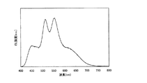
本実施例で作製した発光素子を発光させたときの発光スペクトルを図10に示す。図1
0において横軸は波長(nm)を、縦軸は発光強度(任意単位)を表す。図10から、本
実施例で作製した発光素子は、450nmから620nmの波長域において発光している
ことが分かる。また、0.979mAにおけるCIE色度座標は(x、y)=(0.33
,0.46)であった。このことから、本実施例で作製した発光素子は、白色の発光を呈
するものであることが分かった。
FIG. 10 shows an emission spectrum when the light-emitting element manufactured in this example emits light. FIG.
In 0, the horizontal axis represents wavelength (nm) and the vertical axis represents emission intensity (arbitrary unit). FIG. 10 shows that the light-emitting element manufactured in this example emits light in the wavelength region of 450 nm to 620 nm. The CIE chromaticity coordinate at 0.979 mA is (x, y) = (0.33
0.46). This indicates that the light-emitting element manufactured in this example exhibits white light emission.
以上のような本実施例の発光素子は、モリブデン酸化物のような吸水性の低い物質を用
いて作製されている為、水分の混入に起因した発光素子の劣化が少ない。また、本実施例
の発光素子は、白色の発光を呈することがでる。さらに、本実施例の発光素子は、発光し
た光と反射光との干渉が少ない為、発光した光の色度の調整をし易い。
Since the light-emitting element of this embodiment as described above is manufactured using a material having low water absorption such as molybdenum oxide, the light-emitting element is hardly deteriorated due to the mixing of moisture. In addition, the light-emitting element of this example can emit white light. Furthermore, since the light emitting element of this embodiment has little interference between the emitted light and the reflected light, it is easy to adjust the chromaticity of the emitted light.
本実施例では、モリブデン酸化物が、α−NPDに対し、電子受容性の物質として作用
しているかについて調べた実験結果を示す。
In this example, experimental results of examining whether molybdenum oxide acts as an electron-accepting substance on α-NPD are shown.
実験としては、α−NPDとモリブデン酸化物とを含む層302と同様の構成の薄膜(
A)、モリブデン酸化物からなる薄膜(B)、α−NPDからなる薄膜(C)の3種類の
薄膜を真空蒸着によりガラス基板上に形成し、それぞれの透過スペクトルを比較した。
As an experiment, a thin film having the same structure as the
Three types of thin films, A), a thin film made of molybdenum oxide (B), and a thin film made of α-NPD (C), were formed on a glass substrate by vacuum deposition, and their transmission spectra were compared.
実験結果を図11に示す。横軸が波長、縦軸が透過率である。図11に示す通り、α−
NPDとモリブデン酸化物とを含む層302(実施例1に記載)と同様の構成の薄膜(A
)は、モリブデン酸化物からなる薄膜(B)やα−NPDからなる薄膜(C)には見られ
ないブロードなピークが500nm付近(図中、破線で囲まれた領域)に見られる。これ
は、モリブデン酸化物がα−NPDから電子を受け取る電子移動により新たに生じたエネ
ルギー準位であると考えられる。このことから、モリブデン酸化物がα−NPDに対して
電子受容性を示していることがわかった。
The experimental results are shown in FIG. The horizontal axis is wavelength and the vertical axis is transmittance. As shown in FIG.
A thin film having a structure similar to that of the
), A broad peak not seen in the thin film (B) made of molybdenum oxide or the thin film (C) made of α-NPD is seen in the vicinity of 500 nm (region surrounded by a broken line in the figure). This is considered to be an energy level newly generated by electron transfer in which molybdenum oxide receives electrons from α-NPD. From this, it was found that the molybdenum oxide showed an electron accepting property with respect to α-NPD.
101 第1の電極
102 第2の電極
103 第1の層
104 第2の層
111 第1の発光層
121 第2の発光層
201 第1の電極
202 第2の電極
203 第1の層
205 第1の層
207 第1の層
204 第2の層
206 第2の層
208 第2の層
211 第1の発光層
221 第2の発光層
231 第3の発光層
212 正孔輸送層
222 正孔輸送層
232 正孔輸送層
213 電子輸送層
223 電子輸送層
233 電子輸送層
6500 基板
6503 FPC
6504 プリント配線基盤(PWB)
6511 画素部
6512 ソース信号線駆動回路
6513 書込用ゲート信号線駆動回路
6514 消去用ゲート信号線駆動回路
901 第1のトランジスタ
902 第2のトランジスタ
903 発光素子
911 ゲート信号線
912 ソース信号線
913 書込用ゲート信号線駆動回路
914 消去用ゲート信号線駆動回路
915 ソース信号線駆動回路
916 電源
917 電流供給線
918 スイッチ
919 スイッチ
920 スイッチ
1001 第1のトランジスタ
1002 第2のトランジスタ
1003 ゲート信号線
1004 ソース信号線
1005 電流供給線
1006 電極
501 サブフレーム
502 サブフレーム
503 サブフレーム
504 サブフレーム
501a 書き込み期間
501b 保持期間
502a 書き込み期間
502b 保持期間
503a 書き込み期間
503b 保持期間
504a 書き込み期間
504b 保持期間
504c 消去期間
504d 非発光期間
10 基板
11 トランジスタ
12 発光素子
13 第1の電極
14 第2の電極
15 層
16 第1層間絶縁膜
16a 第1層間絶縁膜
16b 第1層間絶縁膜
16c 第1層間絶縁膜
17 配線
18 隔壁層
19 第2層間絶縁膜
5521 本体
5522 筐体
5523 表示部
5524 キーボード
5551 表示部
5552 本体
5553 アンテナ
5554 音声出力部
5555 音声入力部
5556 操作スイッチ
5531 表示部
5532 筐体
5533 スピーカー
300 基板
301 層
302 層
303 層
304 層
305 層
306 層
307 層
308 層
309 層
310 層
311 層
312 層
313 層
314 層
315 層
316 層
317 層
101
6504 Printed Wiring Board (PWB)
6511 Pixel portion 6512 Source signal line driving circuit 6513 Writing gate signal line driving circuit 6514 Erasing gate signal line driving circuit 901 First transistor 902 Second transistor 903 Light emitting element 911 Gate signal line 912 Source signal line 913 Writing Gate signal line driving circuit 914 erasing gate signal line driving circuit 915 source signal line driving circuit 916 power supply 917 current supply line 918 switch 919 switch 920 switch 1001 first transistor 1002 second transistor 1003 gate signal line 1004 source signal line 1005 Current supply line 1006 Electrode 501 Subframe 502 Subframe 503 Subframe 504 Subframe 501a Writing period 501b Holding period 502a Writing period 502b Holding period 503a Writing Only period 503b holding period 504a writing period 504b holding period 504c erasing period 504d non-light emitting period 10 substrate 11 transistor 12 light emitting element 13 first electrode 14 second electrode 15 layer 16 first interlayer insulating film 16a first interlayer insulating film 16b First interlayer insulating film 16c First interlayer insulating film 17 Wiring 18 Partition layer 19 Second interlayer insulating film 5521 Main body 5522 Housing 5523 Display unit 5524 Keyboard 5551 Display unit 5552 Main unit 5553 Antenna 5554 Audio output unit 5555 Audio input unit 5556 Operation switch 5531 Display portion 5532 Housing 5533 Speaker 300 Substrate 301 Layer 302 Layer 303 Layer 304 Layer 305 Layer 306 Layer 307 Layer 308 Layer 309 Layer 310 Layer 311 Layer 312 Layer 313 Layer 314 Layer 315 Layer 316 Layer 317 Layer
Claims (1)
信号線と、
電位を供給することができる機能を有する配線と、
第1のトランジスタと、
第2のトランジスタと、
第1の電極と、第2の電極と、前記第1の電極と前記第2の電極に挟持された発光層と、を有する発光素子と、
を有する表示装置であって、
前記走査線は前記第1のトランジスタのゲートに電気的に接続され、
前記信号線は前記第1のトランジスタのソースまたはドレインの一方に電気的に接続され、
前記第1のトランジスタのソースまたはドレインの他方は、前記第2のトランジスタのゲートに電気的に接続され、
前記第2のトランジスタのソースまたはドレインの一方は、前記電位の供給することができる機能を有する配線に電気的に接続され、
前記第2のトランジスタのソースまたはドレインの他方は、前記第1の電極に電気的に接続され、
前記第1のトランジスタ及び第2のトランジスタはnチャネル型であり、
前記第1のトランジスタと前記第2のトランジスタは結晶質を有し、
第1の電極から第2の電極に向かって1番目からn番目(nは2以上の整数)までのn個の発光層が積層され、
m番目(mは1≦m≦(n−1)の整数)の発光層と(m+1)番目の発光層との間には、第1の薄膜と第2の薄膜が設けられ、
前記第1の薄膜と前記第2の薄膜は接しており、
前記m番目の発光層と前記(m+1)番目の発光層との間に設けられた前記第1の薄膜は、前記m番目の発光層に電子を注入し、
前記m番目の発光層と前記(m+1)番目の発光層との間に設けられた前記第2の薄膜は、前記(m+1)番目の発光層に正孔を注入し、
前記第1の薄膜は、電子輸送性の物質と電子供与性の物質を含む薄膜であり、
前記第2の薄膜は、正孔輸送性の物質とモリブデン酸化物を含む薄膜(前記正孔輸送性の物質に対して前記モリブデン酸化物が0.01〜10容量%の濃度であることを除く)であることを特徴とする表示装置。 Scanning lines;
A signal line;
A wiring having a function of supplying a potential;
A first transistor;
A second transistor;
A light-emitting element having a first electrode, a second electrode, and a light-emitting layer sandwiched between the first electrode and the second electrode;
A display device comprising:
The scan line is electrically connected to a gate of the first transistor;
The signal line is electrically connected to one of a source and a drain of the first transistor;
The other of the source and the drain of the first transistor is electrically connected to the gate of the second transistor;
One of a source and a drain of the second transistor is electrically connected to a wiring having a function of supplying the potential,
The other of the source and the drain of the second transistor is electrically connected to the first electrode;
The first transistor and the second transistor are n-channel type,
The first transistor and the second transistor have crystallinity ,
From the first electrode to the second electrode, the first to nth (n is an integer of 2 or more) n light emitting layers are stacked,
A first thin film and a second thin film are provided between the mth light emitting layer (m is an integer of 1 ≦ m ≦ (n−1)) and the (m + 1) th light emitting layer,
The first thin film and the second thin film are in contact with each other;
The first thin film provided between the mth light emitting layer and the (m + 1) th light emitting layer injects electrons into the mth light emitting layer,
The second thin film provided between the mth light emitting layer and the (m + 1) th light emitting layer injects holes into the (m + 1) th light emitting layer,
The first thin film is a thin film containing an electron transporting substance and an electron donating substance,
The second thin film is a thin film containing a hole transporting substance and molybdenum oxide (except that the molybdenum oxide has a concentration of 0.01 to 10% by volume with respect to the hole transporting substance). ).
Priority Applications (1)
| Application Number | Priority Date | Filing Date | Title |
|---|---|---|---|
| JP2013169399A JP5640124B2 (en) | 2004-05-21 | 2013-08-19 | Display device |
Applications Claiming Priority (3)
| Application Number | Priority Date | Filing Date | Title |
|---|---|---|---|
| JP2004152491 | 2004-05-21 | ||
| JP2004152491 | 2004-05-21 | ||
| JP2013169399A JP5640124B2 (en) | 2004-05-21 | 2013-08-19 | Display device |
Related Parent Applications (1)
| Application Number | Title | Priority Date | Filing Date |
|---|---|---|---|
| JP2012117680A Division JP5589025B2 (en) | 2004-05-21 | 2012-05-23 | Light emitting element |
Publications (2)
| Publication Number | Publication Date |
|---|---|
| JP2013239460A JP2013239460A (en) | 2013-11-28 |
| JP5640124B2 true JP5640124B2 (en) | 2014-12-10 |
Family
ID=35428703
Family Applications (4)
| Application Number | Title | Priority Date | Filing Date |
|---|---|---|---|
| JP2005145096A Expired - Fee Related JP4667955B2 (en) | 2004-05-21 | 2005-05-18 | LIGHT EMITTING ELEMENT, LIGHT EMITTING DEVICE, AND LIGHTING EQUIPMENT |
| JP2010132978A Expired - Fee Related JP5346880B2 (en) | 2004-05-21 | 2010-06-10 | LIGHT EMITTING ELEMENT, LIGHT EMITTING DEVICE, AND LIGHTING EQUIPMENT |
| JP2012117680A Active JP5589025B2 (en) | 2004-05-21 | 2012-05-23 | Light emitting element |
| JP2013169399A Expired - Fee Related JP5640124B2 (en) | 2004-05-21 | 2013-08-19 | Display device |
Family Applications Before (3)
| Application Number | Title | Priority Date | Filing Date |
|---|---|---|---|
| JP2005145096A Expired - Fee Related JP4667955B2 (en) | 2004-05-21 | 2005-05-18 | LIGHT EMITTING ELEMENT, LIGHT EMITTING DEVICE, AND LIGHTING EQUIPMENT |
| JP2010132978A Expired - Fee Related JP5346880B2 (en) | 2004-05-21 | 2010-06-10 | LIGHT EMITTING ELEMENT, LIGHT EMITTING DEVICE, AND LIGHTING EQUIPMENT |
| JP2012117680A Active JP5589025B2 (en) | 2004-05-21 | 2012-05-23 | Light emitting element |
Country Status (5)
| Country | Link |
|---|---|
| US (4) | US7598670B2 (en) |
| JP (4) | JP4667955B2 (en) |
| KR (3) | KR101152935B1 (en) |
| CN (3) | CN101640254B (en) |
| WO (1) | WO2005115060A1 (en) |
Families Citing this family (44)
| Publication number | Priority date | Publication date | Assignee | Title |
|---|---|---|---|---|
| US8018152B2 (en) | 2004-05-20 | 2011-09-13 | Semiconductor Energy Laboratory Co., Ltd. | Light-emitting element including intermediate conductive layer having a hole-injection layer with an island-like structure |
| CN101640254B (en) | 2004-05-21 | 2016-01-20 | 株式会社半导体能源研究所 | Light-emitting component and luminaire |
| WO2005115059A1 (en) * | 2004-05-21 | 2005-12-01 | Semiconductor Energy Laboratory Co., Ltd. | Light emitting element and light emitting device using the element |
| JP4925569B2 (en) * | 2004-07-08 | 2012-04-25 | ローム株式会社 | Organic electroluminescent device |
| US7952089B2 (en) | 2004-10-22 | 2011-05-31 | Semiconductor Energy Laboratory Co., Ltd. | Composite material and light emitting element |
| US7564052B2 (en) * | 2004-11-05 | 2009-07-21 | Semiconductor Energy Laboratory Co., Ltd. | Light-emitting element and light emitting device using the same |
| KR101210858B1 (en) | 2004-11-05 | 2012-12-11 | 가부시키가이샤 한도오따이 에네루기 켄큐쇼 | Light emitting element and light emitting device using the same |
| JP4939809B2 (en) | 2005-01-21 | 2012-05-30 | 株式会社半導体エネルギー研究所 | Light emitting device |
| JP2006269351A (en) * | 2005-03-25 | 2006-10-05 | Aitesu:Kk | Top emission multiphoton organic el display panel |
| JP4802896B2 (en) * | 2005-09-09 | 2011-10-26 | セイコーエプソン株式会社 | Manufacturing method of electro-optical device |
| EP1784055A3 (en) * | 2005-10-17 | 2009-08-05 | Semiconductor Energy Laboratory Co., Ltd. | Lighting system |
| KR100774200B1 (en) * | 2006-04-13 | 2007-11-08 | 엘지전자 주식회사 | Organic Electroluminescence Device and method for fabricating the same |
| JP5030742B2 (en) * | 2006-11-30 | 2012-09-19 | 株式会社半導体エネルギー研究所 | Light emitting element |
| JP4939284B2 (en) * | 2007-04-05 | 2012-05-23 | 財団法人山形県産業技術振興機構 | Organic electroluminescent device |
| US8384283B2 (en) * | 2007-09-20 | 2013-02-26 | Semiconductor Energy Laboratory Co., Ltd. | Light-emitting element, light-emitting device, and electronic device |
| TWI606520B (en) | 2008-10-31 | 2017-11-21 | 半導體能源研究所股份有限公司 | Semiconductor device and method for manufacturing the same |
| TWI486097B (en) | 2008-12-01 | 2015-05-21 | Semiconductor Energy Lab | Light-emitting element, light-emitting device, lighting device, and electronic device |
| KR101648927B1 (en) | 2009-01-16 | 2016-08-17 | 가부시키가이샤 한도오따이 에네루기 켄큐쇼 | Semiconductor device and manufacturing method thereof |
| KR101671210B1 (en) | 2009-03-06 | 2016-11-01 | 가부시키가이샤 한도오따이 에네루기 켄큐쇼 | Semiconductor device and method for manufacturing the same |
| JP5676867B2 (en) * | 2009-09-29 | 2015-02-25 | 住友化学株式会社 | Organic electroluminescence device |
| JP5573127B2 (en) * | 2009-11-27 | 2014-08-20 | セイコーエプソン株式会社 | LIGHT EMITTING ELEMENT, DISPLAY DEVICE, AND ELECTRONIC DEVICE |
| EP2365556B1 (en) * | 2010-03-08 | 2014-07-23 | Semiconductor Energy Laboratory Co., Ltd. | Light-emitting element, light-emitting device, electronic device, and lighting device |
| CN102201541B (en) | 2010-03-23 | 2015-11-25 | 株式会社半导体能源研究所 | Light-emitting component, light-emitting device, electronic equipment and lighting device |
| JP5801579B2 (en) | 2010-03-31 | 2015-10-28 | 株式会社半導体エネルギー研究所 | LIGHT EMITTING ELEMENT, LIGHT EMITTING DEVICE, ELECTRONIC DEVICE, AND LIGHTING DEVICE |
| TWI506121B (en) | 2010-03-31 | 2015-11-01 | Semiconductor Energy Lab | Light-emitting element, light-emitting device, electronic device, and lighting device |
| WO2012046560A1 (en) | 2010-10-04 | 2012-04-12 | Semiconductor Energy Laboratory Co., Ltd. | Composite material, light-emitting element, light-emitting device, electronic device, and lighting device |
| TWI518078B (en) * | 2010-12-28 | 2016-01-21 | 半導體能源研究所股份有限公司 | Benzo(b)naphtho(1,2-d)furan compound as light-emitting element material |
| JP2012186092A (en) * | 2011-03-07 | 2012-09-27 | Seiko Epson Corp | Light-emitting element, light-emitting device, display device, and electronic apparatus |
| JP2012227122A (en) * | 2011-04-04 | 2012-11-15 | Rohm Co Ltd | Organic el device |
| JP5879741B2 (en) * | 2011-05-02 | 2016-03-08 | セイコーエプソン株式会社 | LIGHT EMITTING ELEMENT, DISPLAY DEVICE, AND ELECTRONIC DEVICE |
| JP6023461B2 (en) | 2011-05-13 | 2016-11-09 | 株式会社半導体エネルギー研究所 | Light emitting element, light emitting device |
| TWI651878B (en) * | 2012-08-03 | 2019-02-21 | 日商半導體能源研究所股份有限公司 | Light-emitting element, light-emitting device, display device, electronic device and lighting device |
| JP6351947B2 (en) | 2012-10-12 | 2018-07-04 | 株式会社半導体エネルギー研究所 | Method for manufacturing liquid crystal display device |
| TWI681233B (en) | 2012-10-12 | 2020-01-01 | 日商半導體能源研究所股份有限公司 | Liquid crystal display device, touch panel and method for manufacturing liquid crystal display device |
| TWI582993B (en) | 2012-11-30 | 2017-05-11 | 半導體能源研究所股份有限公司 | Semiconductor device |
| CN104078568A (en) * | 2013-03-29 | 2014-10-01 | 海洋王照明科技股份有限公司 | Organic light-emitting diode and preparation method thereof |
| TWI632688B (en) | 2013-07-25 | 2018-08-11 | 半導體能源研究所股份有限公司 | Semiconductor device and method for manufacturing semiconductor device |
| TWI713447B (en) | 2014-04-30 | 2020-12-21 | 日商半導體能源研究所股份有限公司 | Light-emitting element, light-emitting device, lighting device, and electronic appliance |
| JP6522311B2 (en) * | 2014-10-17 | 2019-05-29 | パイオニア株式会社 | Light emitting device |
| US9660220B2 (en) * | 2014-10-24 | 2017-05-23 | Semiconductor Energy Laboratory Co., Ltd. | Multiple light-emitting element device |
| JPWO2016092883A1 (en) * | 2014-12-08 | 2017-04-27 | 株式会社Joled | Display element, display device, and electronic device |
| CN104678617A (en) * | 2015-03-20 | 2015-06-03 | 京东方科技集团股份有限公司 | Testing device, manufacturing thereof and display device |
| US10340470B2 (en) | 2016-02-23 | 2019-07-02 | Semiconductor Energy Laboratory Co., Ltd. | Light-emitting element, display device, electronic device, and lighting apparatus |
| EP3517563B1 (en) | 2017-10-12 | 2022-04-13 | Kureha Corporation | Continuous polymerization device and continuous production method for polymer |
Family Cites Families (49)
| Publication number | Priority date | Publication date | Assignee | Title |
|---|---|---|---|---|
| US603384A (en) * | 1898-05-03 | Steam-engine | ||
| JPH0719925B2 (en) * | 1985-03-05 | 1995-03-06 | 株式会社東芝 | Conductive thin film |
| JPH0541285A (en) * | 1991-08-07 | 1993-02-19 | Ricoh Co Ltd | Electroluminescence element |
| JP2824411B2 (en) | 1995-08-25 | 1998-11-11 | 株式会社豊田中央研究所 | Organic thin-film light emitting device |
| US5849403A (en) | 1995-09-13 | 1998-12-15 | Kabushiki Kaisha Toshiba | Organic thin film device |
| JPH10270171A (en) | 1997-01-27 | 1998-10-09 | Junji Kido | Organic electroluminescent element |
| JP4486713B2 (en) | 1997-01-27 | 2010-06-23 | 淳二 城戸 | Organic electroluminescent device |
| JPH11251067A (en) | 1998-03-02 | 1999-09-17 | Junji Kido | Organic electroluminescence element |
| JPH11307264A (en) | 1998-04-17 | 1999-11-05 | Matsushita Electric Ind Co Ltd | Organic electroluminescent element |
| JPH11307259A (en) | 1998-04-23 | 1999-11-05 | Tdk Corp | Organic el element |
| JP3875401B2 (en) * | 1998-05-12 | 2007-01-31 | Tdk株式会社 | Organic EL display device and organic EL element |
| US6885147B2 (en) * | 1998-05-18 | 2005-04-26 | Emagin Corporation | Organic light emitting diode devices with improved anode stability |
| JP3884564B2 (en) | 1998-05-20 | 2007-02-21 | 出光興産株式会社 | Organic EL light emitting device and light emitting device using the same |
| CA2348641A1 (en) * | 1998-08-31 | 2001-04-19 | The Government Of The United States Of America As Represented By The Secretary Of The Navy | Coated cathodoluminescent phosphors |
| JP3885412B2 (en) | 1999-05-25 | 2007-02-21 | 松下電器産業株式会社 | Organic electroluminescence device |
| JP4824848B2 (en) * | 2000-02-29 | 2011-11-30 | 淳二 城戸 | Organic electroluminescent device, organic electroluminescent device group, and method for identifying emission spectrum thereof |
| KR20010050711A (en) | 1999-09-29 | 2001-06-15 | 준지 키도 | Organic electroluminescent device, group of organic electroluminescent devices and controlling method of emission spectrum in such devices |
| KR20010085420A (en) | 2000-02-23 | 2001-09-07 | 기타지마 요시토시 | Electroluminescence element and method manufacturing the same |
| KR100329571B1 (en) | 2000-03-27 | 2002-03-23 | 김순택 | Organic electroluminescent device |
| JP4617019B2 (en) | 2000-04-25 | 2011-01-19 | 大日本印刷株式会社 | EL device having photocatalyst containing layer and method for producing the same |
| JP4611578B2 (en) | 2001-07-26 | 2011-01-12 | 淳二 城戸 | Organic electroluminescent device |
| JP2003045661A (en) * | 2001-08-02 | 2003-02-14 | Fuji Photo Film Co Ltd | Light-emitting nanostructure and light-emitting element using the same |
| JP2003068472A (en) * | 2001-08-29 | 2003-03-07 | Hitachi Ltd | Organic light-emitting element and organic light-emitting display using it |
| SG113443A1 (en) | 2001-12-05 | 2005-08-29 | Semiconductor Energy Laboratao | Organic semiconductor element |
| JP2003264085A (en) | 2001-12-05 | 2003-09-19 | Semiconductor Energy Lab Co Ltd | Organic semiconductor element, organic electroluminescence element and organic solar cell |
| JP2003217839A (en) | 2002-01-22 | 2003-07-31 | Seiko Epson Corp | Material arranging method, film forming device, electro- optic device, manufacturing method for it, electronic device and electronics |
| JP2003217863A (en) * | 2002-01-22 | 2003-07-31 | Honda Motor Co Ltd | Method of fabricating organic electroluminescent element |
| US6872472B2 (en) | 2002-02-15 | 2005-03-29 | Eastman Kodak Company | Providing an organic electroluminescent device having stacked electroluminescent units |
| JP3933591B2 (en) | 2002-03-26 | 2007-06-20 | 淳二 城戸 | Organic electroluminescent device |
| KR20030086165A (en) * | 2002-05-03 | 2003-11-07 | 엘지.필립스 엘시디 주식회사 | The organic electro-luminescence device and method for fabricating of the same |
| EP1367659B1 (en) | 2002-05-21 | 2012-09-05 | Semiconductor Energy Laboratory Co., Ltd. | Organic field effect transistor |
| EP1388903B1 (en) | 2002-08-09 | 2016-03-16 | Semiconductor Energy Laboratory Co., Ltd. | Organic electroluminescent device |
| TWI272874B (en) | 2002-08-09 | 2007-02-01 | Semiconductor Energy Lab | Organic electroluminescent device |
| JP2004134395A (en) | 2002-09-20 | 2004-04-30 | Matsushita Electric Ind Co Ltd | Organic electroluminescence element, exposure device using the same, and image forming apparatus |
| US7158161B2 (en) | 2002-09-20 | 2007-01-02 | Matsushita Electric Industrial Co., Ltd. | Organic electroluminescence element and an exposure unit and image-forming apparatus both using the element |
| US20040161192A1 (en) | 2002-12-18 | 2004-08-19 | Matsushita Electric Industrial Co., Ltd. | Exposing apparatus and image forming apparatus using organic electroluminescence element |
| US6936961B2 (en) | 2003-05-13 | 2005-08-30 | Eastman Kodak Company | Cascaded organic electroluminescent device having connecting units with N-type and P-type organic layers |
| JP2005026121A (en) | 2003-07-03 | 2005-01-27 | Fujitsu Ltd | Organic el element and manufacturing method of the same as well as organic el display |
| AU2003294180A1 (en) | 2003-07-09 | 2005-01-28 | Matsushita Electric Industrial Co., Ltd. | Organic electroluminescence element and an exposure unit and image-forming apparatus both using the element |
| TW200513138A (en) * | 2003-09-23 | 2005-04-01 | Guan-Chang Peng | Organic light Emitting Device (OLED) |
| CN101789497B (en) | 2003-09-26 | 2013-03-13 | 株式会社半导体能源研究所 | Light-emitting device and method for manufacturing the same |
| JP4476594B2 (en) | 2003-10-17 | 2010-06-09 | 淳二 城戸 | Organic electroluminescent device |
| US7205716B2 (en) * | 2003-10-20 | 2007-04-17 | Semiconductor Energy Laboratory Co., Ltd. | Light-emitting device |
| JP2005135600A (en) * | 2003-10-28 | 2005-05-26 | Idemitsu Kosan Co Ltd | Organic electroluminescent element |
| JP4243237B2 (en) * | 2003-11-10 | 2009-03-25 | 淳二 城戸 | Organic element, organic EL element, organic solar cell, organic FET structure, and organic element manufacturing method |
| JP4300176B2 (en) | 2003-11-13 | 2009-07-22 | ローム株式会社 | Organic electroluminescent device |
| EP2059094A1 (en) | 2003-12-16 | 2009-05-13 | Panasonic Corporation | Organic electroluminescent device and method for manufacturing the same |
| CN101640254B (en) * | 2004-05-21 | 2016-01-20 | 株式会社半导体能源研究所 | Light-emitting component and luminaire |
| JP4925569B2 (en) | 2004-07-08 | 2012-04-25 | ローム株式会社 | Organic electroluminescent device |
-
2005
- 2005-05-17 CN CN200910164536.6A patent/CN101640254B/en active Active
- 2005-05-17 KR KR1020067025936A patent/KR101152935B1/en active IP Right Grant
- 2005-05-17 CN CN2009101645370A patent/CN101640216B/en active Active
- 2005-05-17 CN CNB2005800246227A patent/CN100531497C/en active Active
- 2005-05-17 KR KR1020107010378A patent/KR101152947B1/en active IP Right Grant
- 2005-05-17 KR KR1020117022763A patent/KR101187402B1/en active IP Right Grant
- 2005-05-17 WO PCT/JP2005/009313 patent/WO2005115060A1/en active Application Filing
- 2005-05-17 US US10/593,193 patent/US7598670B2/en active Active
- 2005-05-18 JP JP2005145096A patent/JP4667955B2/en not_active Expired - Fee Related
-
2009
- 2009-09-21 US US12/563,242 patent/US7940002B2/en active Active
-
2010
- 2010-06-10 JP JP2010132978A patent/JP5346880B2/en not_active Expired - Fee Related
-
2011
- 2011-05-05 US US13/101,572 patent/US8344621B2/en active Active
-
2012
- 2012-05-23 JP JP2012117680A patent/JP5589025B2/en active Active
- 2012-12-31 US US13/731,442 patent/US8922116B2/en active Active
-
2013
- 2013-08-19 JP JP2013169399A patent/JP5640124B2/en not_active Expired - Fee Related
Also Published As
| Publication number | Publication date |
|---|---|
| KR20100055546A (en) | 2010-05-26 |
| CN101023708A (en) | 2007-08-22 |
| CN100531497C (en) | 2009-08-19 |
| US8922116B2 (en) | 2014-12-30 |
| KR101152935B1 (en) | 2012-06-08 |
| CN101640254A (en) | 2010-02-03 |
| JP2013239460A (en) | 2013-11-28 |
| CN101640216B (en) | 2011-09-28 |
| JP4667955B2 (en) | 2011-04-13 |
| JP2012156148A (en) | 2012-08-16 |
| JP5346880B2 (en) | 2013-11-20 |
| US20110272690A1 (en) | 2011-11-10 |
| KR101187402B1 (en) | 2012-10-02 |
| JP5589025B2 (en) | 2014-09-10 |
| JP2010192465A (en) | 2010-09-02 |
| JP2006013458A (en) | 2006-01-12 |
| US8344621B2 (en) | 2013-01-01 |
| US7940002B2 (en) | 2011-05-10 |
| CN101640216A (en) | 2010-02-03 |
| WO2005115060A1 (en) | 2005-12-01 |
| US20100033090A1 (en) | 2010-02-11 |
| KR20070026570A (en) | 2007-03-08 |
| US20130214256A1 (en) | 2013-08-22 |
| KR101152947B1 (en) | 2012-06-08 |
| KR20110111548A (en) | 2011-10-11 |
| US20070182318A1 (en) | 2007-08-09 |
| CN101640254B (en) | 2016-01-20 |
| US7598670B2 (en) | 2009-10-06 |
Similar Documents
| Publication | Publication Date | Title |
|---|---|---|
| JP5640124B2 (en) | Display device | |
| JP6039007B2 (en) | Light emitting element, light emitting device, lighting device, electronic device | |
| US8815419B2 (en) | Light emitting device and electronic appliance using the same | |
| US9263645B2 (en) | Light-emitting element, light-emitting device, and electronic device | |
| JP5072271B2 (en) | LIGHT EMITTING DEVICE AND ELECTRONIC DEVICE USING THE SAME | |
| JP5314834B2 (en) | LIGHT EMITTING ELEMENT, LIGHT EMITTING DEVICE, LIGHTING DEVICE, AND ELECTRONIC DEVICE | |
| US7667389B2 (en) | Light emitting element, light emitting device, and electronic device | |
| JP4799111B2 (en) | Light emitting device | |
| JP4789706B2 (en) | Light-emitting element, light-emitting device, electronic device | |
| JP4789598B2 (en) | LIGHT EMITTING ELEMENT AND ELECTRONIC DEVICE |
Legal Events
| Date | Code | Title | Description |
|---|---|---|---|
| A977 | Report on retrieval |
Free format text: JAPANESE INTERMEDIATE CODE: A971007 Effective date: 20140519 |
|
| A131 | Notification of reasons for refusal |
Free format text: JAPANESE INTERMEDIATE CODE: A131 Effective date: 20140527 |
|
| A521 | Request for written amendment filed |
Free format text: JAPANESE INTERMEDIATE CODE: A523 Effective date: 20140716 |
|
| TRDD | Decision of grant or rejection written | ||
| A01 | Written decision to grant a patent or to grant a registration (utility model) |
Free format text: JAPANESE INTERMEDIATE CODE: A01 Effective date: 20141021 |
|
| A61 | First payment of annual fees (during grant procedure) |
Free format text: JAPANESE INTERMEDIATE CODE: A61 Effective date: 20141027 |
|
| R150 | Certificate of patent or registration of utility model |
Ref document number: 5640124 Country of ref document: JP Free format text: JAPANESE INTERMEDIATE CODE: R150 |
|
| R250 | Receipt of annual fees |
Free format text: JAPANESE INTERMEDIATE CODE: R250 |
|
| R250 | Receipt of annual fees |
Free format text: JAPANESE INTERMEDIATE CODE: R250 |
|
| R250 | Receipt of annual fees |
Free format text: JAPANESE INTERMEDIATE CODE: R250 |
|
| R250 | Receipt of annual fees |
Free format text: JAPANESE INTERMEDIATE CODE: R250 |
|
| R250 | Receipt of annual fees |
Free format text: JAPANESE INTERMEDIATE CODE: R250 |
|
| LAPS | Cancellation because of no payment of annual fees |