JP5522012B2 - Capacitance element characteristic measuring method and characteristic measuring apparatus - Google Patents
Capacitance element characteristic measuring method and characteristic measuring apparatus Download PDFInfo
- Publication number
- JP5522012B2 JP5522012B2 JP2010275204A JP2010275204A JP5522012B2 JP 5522012 B2 JP5522012 B2 JP 5522012B2 JP 2010275204 A JP2010275204 A JP 2010275204A JP 2010275204 A JP2010275204 A JP 2010275204A JP 5522012 B2 JP5522012 B2 JP 5522012B2
- Authority
- JP
- Japan
- Prior art keywords
- capacitive element
- voltage
- characteristic measuring
- ceramic capacitor
- cooling
- Prior art date
- Legal status (The legal status is an assumption and is not a legal conclusion. Google has not performed a legal analysis and makes no representation as to the accuracy of the status listed.)
- Active
Links
- 238000000034 method Methods 0.000 title claims description 39
- 238000005259 measurement Methods 0.000 claims description 39
- 238000001816 cooling Methods 0.000 claims description 33
- 238000010438 heat treatment Methods 0.000 claims description 24
- 239000003990 capacitor Substances 0.000 claims description 22
- 238000007599 discharging Methods 0.000 claims description 19
- 239000000463 material Substances 0.000 claims description 15
- 239000003985 ceramic capacitor Substances 0.000 description 57
- 230000010287 polarization Effects 0.000 description 39
- 238000009413 insulation Methods 0.000 description 15
- 230000005684 electric field Effects 0.000 description 14
- 239000013078 crystal Substances 0.000 description 10
- 238000007689 inspection Methods 0.000 description 10
- 230000002269 spontaneous effect Effects 0.000 description 9
- 238000010586 diagram Methods 0.000 description 8
- RKTYLMNFRDHKIL-UHFFFAOYSA-N copper;5,10,15,20-tetraphenylporphyrin-22,24-diide Chemical compound [Cu+2].C1=CC(C(=C2C=CC([N-]2)=C(C=2C=CC=CC=2)C=2C=CC(N=2)=C(C=2C=CC=CC=2)C2=CC=C3[N-]2)C=2C=CC=CC=2)=NC1=C3C1=CC=CC=C1 RKTYLMNFRDHKIL-UHFFFAOYSA-N 0.000 description 6
- 238000000691 measurement method Methods 0.000 description 4
- 238000000926 separation method Methods 0.000 description 4
- JRPBQTZRNDNNOP-UHFFFAOYSA-N barium titanate Chemical compound [Ba+2].[Ba+2].[O-][Ti]([O-])([O-])[O-] JRPBQTZRNDNNOP-UHFFFAOYSA-N 0.000 description 3
- 229910002113 barium titanate Inorganic materials 0.000 description 3
- 230000007423 decrease Effects 0.000 description 3
- 230000002950 deficient Effects 0.000 description 3
- 238000012360 testing method Methods 0.000 description 3
- 238000007796 conventional method Methods 0.000 description 2
- 230000000704 physical effect Effects 0.000 description 2
- 238000010521 absorption reaction Methods 0.000 description 1
- 230000004308 accommodation Effects 0.000 description 1
- 239000000470 constituent Substances 0.000 description 1
- 230000008878 coupling Effects 0.000 description 1
- 238000010168 coupling process Methods 0.000 description 1
- 238000005859 coupling reaction Methods 0.000 description 1
- 230000006378 damage Effects 0.000 description 1
- 230000003111 delayed effect Effects 0.000 description 1
- 230000000694 effects Effects 0.000 description 1
- 238000002474 experimental method Methods 0.000 description 1
- 239000003302 ferromagnetic material Substances 0.000 description 1
- 238000004519 manufacturing process Methods 0.000 description 1
- 238000012986 modification Methods 0.000 description 1
- 230000004048 modification Effects 0.000 description 1
- 238000012545 processing Methods 0.000 description 1
- 230000002336 repolarization Effects 0.000 description 1
- 238000004904 shortening Methods 0.000 description 1
- 239000007787 solid Substances 0.000 description 1
- 238000003860 storage Methods 0.000 description 1
- 239000000126 substance Substances 0.000 description 1
- 230000001629 suppression Effects 0.000 description 1
Images

Landscapes
- Testing Relating To Insulation (AREA)
- Measurement Of Resistance Or Impedance (AREA)
- Testing Electric Properties And Detecting Electric Faults (AREA)
Description
この発明は、容量素子に対する絶縁抵抗計測や耐圧試験等の特性測定方法、および特性測定装置に関する。 The present invention relates to a characteristic measuring method and a characteristic measuring apparatus such as an insulation resistance measurement and a withstand voltage test for a capacitive element.
一般にコンデンサ等の容量素子に要求される特性性能として絶縁抵抗性能や漏洩電流性能があり、コンデンサの製造時には各コンデンサを充電して特性性能が測定され、その測定結果に基づいて良品検査が行われる(例えば、特許文献1,2参照。)。
In general, there are insulation resistance performance and leakage current performance required for capacitor elements such as capacitors. During the manufacture of capacitors, each capacitor is charged and the performance characteristics are measured, and non-defective products are inspected based on the measurement results. (For example, see
コンデンサの構成材料として、セラミックコンデンサのように強誘電体(チタン酸バリウム等)が利用されることがある。一般に強誘電体は結晶構造が常温で正方晶であり、結晶粒の内部に自発分極した領域を持つ。強誘電体では、外部電界が印加されることにより結晶粒内部で自発分極の分極方向が揃い、外部電界が印加されない状態では結晶粒内部で自発分極の分極方向が部分反転する。このような強誘電体を用いたコンデンサにおいては、測定電圧を印加してから充電電流値が収束するまで、比較的長い時間を要することが知られている。 A ferroelectric (such as barium titanate) may be used as a constituent material of the capacitor, such as a ceramic capacitor. In general, a ferroelectric has a tetragonal crystal structure at room temperature, and has a spontaneously polarized region inside the crystal grain. In a ferroelectric, when an external electric field is applied, the polarization direction of the spontaneous polarization is aligned inside the crystal grains, and when the external electric field is not applied, the polarization direction of the spontaneous polarization is partially reversed inside the crystal grains. In a capacitor using such a ferroelectric material, it is known that a relatively long time is required until the charging current value converges after the measurement voltage is applied.
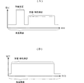
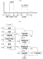
特許文献1には、充電電流値が収束するまでの時間を短縮するため、測定電圧よりも高い電圧の印加・放電を行い、その後、再び測定電圧を印加しなおして特性測定を行う方法が開示されている。図1(A)は、特許文献1に開示された方法の概要を示す電圧パターン図である。
また特許文献2には、長期に亘って高い信頼性を確保できるコンデンサを選別するため、高温環境下で測定電圧を印加し、絶縁抵抗測定を行うことが開示されている。図1(B)は、特許文献2に開示された方法の概要を示す電圧パターン図である。 Patent Document 2 discloses that an insulation resistance measurement is performed by applying a measurement voltage in a high temperature environment in order to select a capacitor that can ensure high reliability over a long period of time. FIG. 1B is a voltage pattern diagram showing an outline of the method disclosed in Patent Document 2.
強誘電体において、充電電流値が収束するまで長時間を要するのは、外部電界の印加によって自発分極の分極方向が外部電界の方向に沿うように変化し、強誘電体の分極がしだいに進行するためである。このような分極は所定の時定数で進行し、分極の進行に伴って電流(分極電流)が流れる。この分極電流は誘電吸収成分とも呼ばれ、この分極電流が存在する間は電圧印加による充電が分極の進行に費やされるため充電電流値の収束が遅くなる。分極電流はコンデンサが大容量であるほど増加するため、大容量のコンデンサであるほど計測中の充電電流値が漏洩電流値に到達するまでに長時間を要することになる。 In ferroelectrics, it takes a long time for the charging current value to converge. The application of an external electric field changes the polarization direction of the spontaneous polarization to follow the direction of the external electric field, and the polarization of the ferroelectric progresses gradually. It is to do. Such polarization proceeds with a predetermined time constant, and a current (polarization current) flows as the polarization progresses. This polarization current is also called a dielectric absorption component, and while the polarization current is present, charging by applying a voltage is consumed for the progress of polarization, so that the convergence of the charging current value is delayed. Since the polarization current increases as the capacity of the capacitor increases, the longer the capacity, the longer it takes for the charging current value being measured to reach the leakage current value.
特許文献1の方法でも、計測中の充電電流値が漏洩電流値に到達するまでの時間は短縮されるが、測定対象となるコンデンサが極めて大容量な場合には、電圧印加の回数を増加させたり、さらに高い電圧を印加したりする必要が生じる。電圧印加の回数を増加させると時間短縮の効果が限定的になり、印加電圧を高めるとコンデンサの破壊が生じる危険性が高くなってしまう。そのため、多数の大容量コンデンサに対して特性測定の検査を実施する場合には、検査時間が増大することで仕掛かり品が増加することになり、検査コストが増加してしまう。
Even in the method of
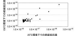
特許文献2に示されたように、高温環境下で絶縁抵抗値を測定する場合、その絶縁抵抗値はJIS規格等の定める常温環境下での絶縁抵抗値に対して完全な相関関係を持つわけではない。図2は、本願の発明者が実験により得た、複数サンプルの常温環境下での絶縁抵抗値と高温環境下での絶縁抵抗値との関係を示す図である。図示するように両者の相関は弱く、このため、常温環境下での絶縁抵抗値を保証するためには、高温環境下での絶縁抵抗試験とはべつに常温環境下でも絶縁抵抗試験を実施する必要があり、検査時間の短縮は困難であった。 As shown in Patent Document 2, when measuring the insulation resistance value in a high temperature environment, the insulation resistance value has a complete correlation with the insulation resistance value in a normal temperature environment defined by JIS standards and the like. is not. FIG. 2 is a diagram showing the relationship between the insulation resistance value in a room temperature environment and the insulation resistance value in a high temperature environment of a plurality of samples obtained by experiments by the inventor of the present application. As shown in the figure, the correlation between the two is weak. Therefore, in order to guarantee the insulation resistance value in the normal temperature environment, it is necessary to perform the insulation resistance test in the normal temperature environment as well as the insulation resistance test in the high temperature environment. Therefore, it was difficult to shorten the inspection time.
そこで本発明の目的は、検査時間を短縮できる容量素子の特性測定方法、および特性測定装置を提供することにある。 SUMMARY OF THE INVENTION An object of the present invention is to provide a characteristic measuring method and characteristic measuring apparatus for a capacitive element that can reduce the inspection time.
この発明の容量素子の特性測定方法は、強誘電体からなる容量素子をキュリー温度以上に加熱する加熱ステップと、キュリー温度以上に加熱した該容量素子に電圧印加して予備充電する予備充電ステップと、予備充電の途中または予備充電の終了後に該容量素子をキュリー温度未満に冷却する冷却ステップと、キュリー温度未満に冷却した該容量素子を放電する放電ステップと、放電後の該容量素子に電圧印加し再充電して特性を測定する再充電・特性測定ステップと、を有する。
予備充電によって強誘電体に対して高温環境下での電界を印加することで、低温環境下で電界を印加する場合よりも強誘電体の分極の進行が加速される。その状態から強誘電体を冷却して放電を行うことで、分極が進んだ状態を維持することができ、その状態から、特性測定を行うために容量素子を再充電することにより、短時間で充電電流値を漏洩電流値に到達させることができる。
The capacitance element characteristic measuring method of the present invention includes a heating step of heating a capacitive element made of a ferroelectric material to a temperature above the Curie temperature, and a preliminary charging step of applying a voltage to the capacitive element heated to a temperature above the Curie temperature and precharging it. A cooling step for cooling the capacitive element to a temperature lower than the Curie temperature during or after the pre-charging, a discharging step for discharging the capacitive element cooled to a temperature lower than the Curie temperature, and applying a voltage to the capacitive element after the discharging. And a recharging / characteristic measuring step for measuring the characteristics by recharging.
By applying an electric field in a high temperature environment to the ferroelectric by precharging, the progress of polarization of the ferroelectric is accelerated as compared with the case of applying an electric field in a low temperature environment. From this state, the ferroelectric material is cooled and discharged to maintain the state of advanced polarization. From that state, the capacitor element can be recharged in order to perform the characteristic measurement. The charging current value can reach the leakage current value.
より詳細には、強誘電体はキュリー温度以上に加熱すると結晶構造が正方晶から立方晶になり一度自発分極が失われる。キュリー温度以上の高温環境下で強誘電体に電界を印加すると、電界に沿った方向の分極が生じる。この状態の強誘電体をキュリー温度よりも低い温度まで冷却すると結晶構造が立方晶から正方晶に戻り、それに伴い電界方向を分極方向とした自発分極が再生する。則ち、キュリー温度以上で予備充電を実施することで、分極を短時間で進めることができる。その状態で放電を行ってから、特性測定を行うために容量素子を再充電することにより、極めて短時間に充電電流値を漏洩電流値に収束させることができる。
なお、キュリー温度よりも高温で放電を行うと、分極が消えた状態で冷却されることになり、立方晶から正方晶に戻る際に自発分極がランダムな向きに生じてしまい、分極を加速させたことにはならない。このため、予備充電に対する放電は冷却後に行うことが重要である。
More specifically, when a ferroelectric is heated to a temperature above the Curie temperature, the crystal structure changes from a tetragonal crystal to a cubic crystal and the spontaneous polarization is lost once. When an electric field is applied to the ferroelectric in a high temperature environment equal to or higher than the Curie temperature, polarization in the direction along the electric field occurs. When the ferroelectric in this state is cooled to a temperature lower than the Curie temperature, the crystal structure returns from cubic to tetragonal, and spontaneous polarization with the electric field direction as the polarization direction is regenerated accordingly. In other words, the polarization can be advanced in a short time by performing the preliminary charging at the Curie temperature or higher. After discharging in this state, the charging current value can be converged to the leakage current value in a very short time by recharging the capacitive element to perform characteristic measurement.
If discharge is performed at a temperature higher than the Curie temperature, it will cool in a state where the polarization has disappeared, and spontaneous polarization will occur in a random direction when returning from cubic to tetragonal, accelerating the polarization. It doesn't matter. For this reason, it is important that the discharge for the precharge is performed after cooling.
上記容量素子の特性測定方法において、前記予備充電ステップでの印加電圧は前記再充電・特性測定ステップで印加する電圧よりも高電圧または同電圧であると望ましい。
充電ステップでの印加電圧が高いほど、前記充電ステップにおいて分極の進行が速まる。
In the method for measuring characteristics of the capacitive element, it is desirable that the applied voltage in the preliminary charging step is higher than or equal to the voltage applied in the recharging / characteristic measuring step.
The higher the applied voltage in the charging step, the faster the polarization progresses in the charging step.
上記容量素子の特性測定方法において、前記予備充電ステップでは、予備充電後に電圧印加用の接触端子を引き離し、前記容量素子の外部端子を開放状態とすると好適である。 In the characteristic measurement method of the capacitive element, in the preliminary charging step, it is preferable that after the preliminary charging, the contact terminal for voltage application is separated and the external terminal of the capacitive element is opened.
この発明の容量素子の特性測定装置は、強誘電体からなる複数の容量素子を供給位置から排出位置まで搬送する搬送路を備える。この搬送路は、加熱領域、予備充電位置、冷却領域、放電位置、再充電・特性測定位置の順に、容量素子を搬送することを特徴とする。なお、加熱領域では容量素子を加熱する。予備充電位置では、前記加熱領域で加熱された容量素子を予備充電する。冷却領域では、前記予備充電位置で充電された前記容量素子を冷却する。放電位置では、前記冷却領域で冷却された前記容量素子を放電する。再充電・特性測定位置では、前記放電位置で放電された前記容量素子を再充電して特性を測定する。
なお、搬送路における加熱領域、予備充電位置、冷却領域、放電位置、再充電・特性測定位置の配置順は、必ずしも明確な境界を持つ必要はない。容量素子の温度環境(キュリー温度以上か未満か)の条件を満足する配置であれば、搬送路中の加熱領域の後半に予備充電位置があってもよいし、冷却領域の後半に放電位置があってもよい。
The capacity element characteristic measuring apparatus according to the present invention includes a transport path for transporting a plurality of capacitative elements made of a ferroelectric material from a supply position to a discharge position. This conveyance path is characterized in that the capacitive element is conveyed in the order of the heating area, the preliminary charging position, the cooling area, the discharging position, and the recharging / characteristic measuring position. Note that the capacitor element is heated in the heating region. At the preliminary charging position, the capacitive element heated in the heating region is precharged. In the cooling region, the capacitive element charged at the preliminary charging position is cooled. At the discharge position, the capacitive element cooled in the cooling region is discharged. At the recharge / characteristic measurement position, the characteristic is measured by recharging the capacitive element discharged at the discharge position.
Note that the order of arrangement of the heating area, the pre-charging position, the cooling area, the discharging position, and the recharging / characteristic measuring position in the conveyance path does not necessarily have a clear boundary. If the arrangement satisfies the conditions of the temperature environment of the capacitive element (whether it is above or below the Curie temperature), there may be a precharge position in the second half of the heating area in the conveyance path, and a discharge position in the second half of the cooling area. There may be.
この発明によれば、強誘電体に高温環境下で電界を印加することにより、比較的短時間に分極を進めることができ、その後に、冷却してから放電を行うことで、分極が進んだ状態を維持することができる。そして、その状態から再充電を行うことにより、充電電流値が漏洩電流値に到達するまでの時間を短縮することができる。これにより、容量素子の検査時間を短縮でき、多数の大容量コンデンサに対して特性測定の全品検査を実施する場合などに、仕掛かり品の増加を抑制し、検査コストを抑制できる。 According to the present invention, polarization can be advanced in a relatively short time by applying an electric field to a ferroelectric material in a high temperature environment, and then polarization is advanced by performing discharge after cooling. The state can be maintained. Then, by performing recharging from that state, the time until the charging current value reaches the leakage current value can be shortened. As a result, the inspection time of the capacitive element can be shortened, and when an inspection of all products for characteristic measurement is performed on a large number of large-capacity capacitors, an increase in work in progress can be suppressed, and the inspection cost can be suppressed.
以下、本発明の実施形態について、容量素子としてセラミックコンデンサを用いる場合を例に説明する。強磁性体からなるセラミックコンデンサの代表例としては、チタン酸バリウム系の固体セラミックコンデンサや積層セラミックコンデンサがある。なお容量素子としては、強誘電体を構成材料とするものであればよく、セラミックコンデンサの他のコンデンサや、圧電デバイス、トランジスタ・FET等の結合容量を持つ素子などを用いても良い。 Hereinafter, embodiments of the present invention will be described by taking a case where a ceramic capacitor is used as a capacitive element as an example. Typical examples of the ceramic capacitor made of a ferromagnetic material include a barium titanate solid ceramic capacitor and a multilayer ceramic capacitor. As the capacitor element, any material may be used as long as it is made of a ferroelectric material, and another capacitor such as a ceramic capacitor, a piezoelectric device, an element having a coupling capacitance such as a transistor / FET, or the like may be used.
《第1の実施形態》
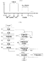
まず、本発明の第1の実施形態に係るセラミックコンデンサの特性測定方法について説明する。図3(A)は本実施形態に係る特性測定方法の概要を示す電圧パターン図であり、図3(B)はそのプロセスフローの一例を示すフローチャートである。
<< First Embodiment >>
First, a method for measuring characteristics of a ceramic capacitor according to the first embodiment of the present invention will be described. FIG. 3A is a voltage pattern diagram showing an outline of the characteristic measurement method according to the present embodiment, and FIG. 3B is a flowchart showing an example of the process flow.
本実施形態の方法では、まず、セラミックコンデンサを加熱設備に供給する(S1)。供給装置としては、振動フィーダまたはバルクカセット式フィーダを用いるとよい。 In the method of this embodiment, first, a ceramic capacitor is supplied to the heating equipment (S1). As the supply device, a vibration feeder or a bulk cassette type feeder may be used.
次に、加熱設備を用いて、セラミックコンデンサをキュリー温度以上に加熱する(S2)。加熱設備としては、内部雰囲気を所定温度に維持する恒温槽や、セラミックコンデンサに押し当てて加熱するホットプレート、非接触でセラミックコンデンサを加熱する赤外線ヒーターなどを利用するとよい。なお、チタン酸バリウム系のセラミックコンデンサの場合には120℃〜150℃以上に加熱すると好適である。その他の材料の場合、各材料に応じたキュリー温度が存在するため、それらに応じて加熱温度は決定すると良い。 Next, using a heating facility, the ceramic capacitor is heated to the Curie temperature or higher (S2). As the heating equipment, a thermostatic bath that maintains the internal atmosphere at a predetermined temperature, a hot plate that is pressed against a ceramic capacitor and heated, an infrared heater that heats the ceramic capacitor in a non-contact manner, and the like may be used. In the case of a barium titanate ceramic capacitor, it is preferable to heat to 120 ° C. to 150 ° C. or higher. In the case of other materials, since there is a Curie temperature corresponding to each material, the heating temperature may be determined accordingly.
次に、セラミックコンデンサにキュリー温度以上の温度を維持させたまま、セラミックコンデンサの外部端子に測定電圧以上の電圧を印加してセラミックコンデンサを予備充電する(S3)。上記電圧の印加時間は、後述する冷却プロセスによってセラミックコンデンサがキュリー温度未満の温度になるまでとしている。これらの条件を満足するのであれば、加熱設備内で予備充電を開始した後に電圧印加状態のままコンデンサを加熱設備から取り出し冷却しても良く、加熱設備で十分に加熱したコンデンサを取り出しキュリー温度以上で予備充電を開始した後に電圧印加状態のまま冷却しても良い。 Next, with the ceramic capacitor maintained at a temperature equal to or higher than the Curie temperature, a voltage higher than the measurement voltage is applied to the external terminal of the ceramic capacitor to precharge the ceramic capacitor (S3). The voltage application time is set until the ceramic capacitor reaches a temperature lower than the Curie temperature by a cooling process described later. If these conditions are satisfied, the capacitor may be taken out of the heating facility and cooled while the voltage is applied after pre-charging is started in the heating facility. Then, after the preliminary charging is started, it may be cooled while the voltage is applied.
次に、セラミックコンデンサをキュリー温度未満の温度、好ましくは常温まで冷却する(S4)。冷却方法として自然冷却を用いることは不可能ではないが、冷却時間の短縮のためには冷却設備を用いることが望ましい。冷却設備としては、所望の温度に設定した恒温槽や、セラミックコンデンサとの接触により冷却するペルチェ素子、非接触で冷却気流をあてる送風器などを用いると良い。 Next, the ceramic capacitor is cooled to a temperature lower than the Curie temperature, preferably to room temperature (S4). Although it is not impossible to use natural cooling as a cooling method, it is desirable to use a cooling facility in order to shorten the cooling time. As a cooling facility, a thermostatic bath set to a desired temperature, a Peltier element that cools by contact with a ceramic capacitor, a blower that applies a cooling airflow in a non-contact manner, or the like may be used.
次に、冷却後のセラミックコンデンサの放電を行う(S5)。コンデンサの放電とは、コンデンサに蓄積された電荷を逃がし、外部端子間の電位差をなくすことである。ここで、コンデンサ内の電荷を完全に放出する必要はなく、放電後の外部端子間の電圧が後工程の再充電・特性測定時の印加電圧よりも低くなっていれば良い。例えば、放電時間によって放電後の外部端子間の電圧値を制御することができる。予め外部端子間の電圧を低くすることにより、再充電・特性測定時の電流の逆流を防止することができる。 Next, the cooled ceramic capacitor is discharged (S5). The discharging of the capacitor is to release the electric charge accumulated in the capacitor and eliminate the potential difference between the external terminals. Here, it is not necessary to completely discharge the electric charge in the capacitor, and it is sufficient that the voltage between the external terminals after discharging is lower than the applied voltage at the time of recharging / characteristic measurement in the subsequent process. For example, the voltage value between the external terminals after discharge can be controlled by the discharge time. By reducing the voltage between the external terminals in advance, it is possible to prevent reverse current flow during recharging and characteristic measurement.
なお、この放電は少なくともキュリー温度よりも低い温度で行う必要がある。仮にキュリー温度以上で放電がされると電圧印加による強誘電体の分極状態が無くなってしまい、冷却時に結晶構造が立方晶から正方晶に戻る際に再生する自発分極の分極方向を電界方向にすることができなくなってしまう。そのため、上述のようにキュリー温度未満で放電を行うことにより、冷却時に結晶構造が立方晶から正方晶に戻る際に再生する自発分極の分極方向を電界方向に沿わせることができる。これにより、後の再充電・特性測定工程において分極に費やされる時間を短縮することができ、測定時間を短縮することが可能になる。 This discharge must be performed at a temperature lower than at least the Curie temperature. If a discharge occurs above the Curie temperature, the polarization state of the ferroelectric material due to voltage application disappears, and the polarization direction of spontaneous polarization that regenerates when the crystal structure returns from cubic to tetragonal during cooling is changed to the electric field direction. It becomes impossible to do. Therefore, by performing discharge at a temperature lower than the Curie temperature as described above, the polarization direction of spontaneous polarization that is regenerated when the crystal structure returns from cubic to tetragonal during cooling can be made to follow the electric field direction. As a result, the time spent for polarization in the subsequent recharging / characteristic measurement step can be shortened, and the measurement time can be shortened.
次に、測定電圧を印加してセラミックコンデンサを再充電させる(S6)。この測定電圧の印加開始時刻からの充電時間を計時し、充電時間が所定の時間になると、充電電流を測定する(S7〜S8)。そして、測定した充電電流値を所定値と比較し、セラミックコンデンサの良否判定を行い、充電電流値が所定値未満、則ち漏洩電流が閾値よりも小さい場合を良品として、逆に漏洩電流が閾値よりも大きい場合を不良品として、判定結果に応じた選別・排出を行う(S9〜S11)。なお、測定した充電電流値から絶縁抵抗値を算出し、絶縁抵抗値を基に良品判定を行っても良い。 Next, a measurement voltage is applied to recharge the ceramic capacitor (S6). The charging time from the application voltage application start time is measured, and when the charging time reaches a predetermined time, the charging current is measured (S7 to S8). Then, the measured charging current value is compared with a predetermined value to determine whether the ceramic capacitor is good or bad. If the charging current value is less than the predetermined value, that is, the leakage current is smaller than the threshold value, the leakage current is the threshold value. If it is larger than that, it is determined as a defective product, and sorting and discharging are performed according to the determination result (S9 to S11). The insulation resistance value may be calculated from the measured charging current value, and the non-defective product determination may be performed based on the insulation resistance value.
図4は、測定電圧を印加することによってセラミックコンデンサに流れる充電電流の測定例を示す波形図であり、予備充電時のセラミックコンデンサの温度を高温(130℃)とした場合と、低温(20℃)とした従来の場合とを比較表示している。同図において横軸には測定電圧を印加してからの時間をLOG表示しており、縦軸には測定された充電電流値をLOG表示している。 FIG. 4 is a waveform diagram showing a measurement example of the charging current flowing in the ceramic capacitor by applying the measurement voltage. The temperature of the ceramic capacitor during the preliminary charging is set to a high temperature (130 ° C.) and the low temperature (20 ° C.). ) And the conventional case. In the figure, the horizontal axis represents the time since the measurement voltage was applied in LOG, and the vertical axis represents the measured charging current value in LOG.
充電電圧の印加当初は、充電電流値は一様であり、その後、急峻に電流値が低下する。そして、次第に電流値の低下傾向が緩やかになり、次第に電流値は一定化していく。予備充電を低温環境下で行った従来の場合(20℃)と、予備充電を高温環境下で行った本実施形態の場合(130℃)とでは、充電電流値の低下速度が異なり、ほぼ全ての時間域に亘って本実施形態のほうが充電電流値は小さい結果であった。 At the beginning of application of the charging voltage, the charging current value is uniform, and then the current value sharply decreases. Then, the current value gradually decreases gradually, and the current value gradually becomes constant. The rate of decrease in the charging current value differs between the conventional case (20 ° C) in which the preliminary charging is performed in a low temperature environment and the case of the present embodiment (130 ° C) in which the preliminary charging is performed in a high temperature environment. In this embodiment, the charging current value was smaller over the time range.
このことから、本実施形態の場合には、従来の場合よりも同一の電流値に到達するまでに要する充電時間が短縮できることがわかる。例えば、従来は約5秒程度かかっていた電流値であっても本実施形態では約1.5秒で到達することができ、充電時間を約30%ほどに短縮することができる。 From this, in the case of the present embodiment, it can be seen that the charging time required to reach the same current value can be shortened as compared with the conventional case. For example, even a current value that previously took about 5 seconds can be reached in about 1.5 seconds in this embodiment, and the charging time can be reduced to about 30%.
このように本実施形態によれば、強誘電体を用いた容量素子において、充電開始から充電電流値が収束するまでの時間を大幅に短縮でき、これにより、容量素子の検査時間と検査コストの抑制を実現することが可能になる。 As described above, according to the present embodiment, in the capacitive element using the ferroelectric, the time from the start of charging to the convergence of the charging current value can be greatly shortened. It becomes possible to realize suppression.
なお、上述した予備充電プロセスはスイッチング電源やシリーズレギュレータ式電源など、どのような電源を用いて行っても良い。一方、測定電圧による再充電プロセスは、物性測定で微小電流を精度良く測定する必要があるため、市販の高抵抗測定器や微小電流測定器などに内蔵される高精度な電圧源を用いると好適である。その他、物性測定で微小電流を精度良く測定することが可能ならば、電圧源を自作しても良く、外部のシリーズレギュレータ式電源から測定電圧を供給したり、スイッチング電源からフィルタを用いてノイズを除去して測定電圧を供給することも可能である。 Note that the above-described precharging process may be performed using any power source such as a switching power source or a series regulator power source. On the other hand, since the recharging process using the measured voltage requires accurate measurement of minute currents by measuring physical properties, it is preferable to use a high-accuracy voltage source built into a commercially available high-resistance measuring device or minute current measuring device. It is. In addition, if it is possible to measure minute currents accurately with physical property measurement, you can make your own voltage source, supply measurement voltage from an external series regulator power supply, or use a filter from a switching power supply to reduce noise. It is also possible to remove and supply the measurement voltage.
《第2の実施形態》
次に、本発明の第2の実施形態に係るセラミックコンデンサの特性測定方法について説明する。図5は、本実施形態に係る特性測定方法の概要を示す電圧パターン図である。
<< Second Embodiment >>
Next, a method for measuring the characteristics of a ceramic capacitor according to a second embodiment of the present invention will be described. FIG. 5 is a voltage pattern diagram showing an outline of the characteristic measuring method according to the present embodiment.
本実施形態は、予備充電プロセスでの印加電圧を測定プロセスでの測定電圧と同電圧とする点で、第1の実施形態と相違する。この場合、予備充電プロセスにおける、強誘電体の分極の進行は第1の実施形態よりも遅いものになり、第1の実施形態よりも検査時間は若干長くなると思われる。しかしながら、少なくとも、予備充電を行わずに常温環境で特性測定を行うような場合よりは検査時間を短縮できる。そして、両プロセスで用いる電圧源を同一のものにすることができるため、昇圧回路等を用いずに簡易な回路構成を用いて容量素子の特性測定を行える。 This embodiment is different from the first embodiment in that the applied voltage in the precharge process is the same voltage as the measurement voltage in the measurement process. In this case, the progress of the polarization of the ferroelectric in the precharging process is slower than that in the first embodiment, and the inspection time seems to be slightly longer than that in the first embodiment. However, the inspection time can be shortened at least as compared with the case where characteristic measurement is performed in a room temperature environment without performing preliminary charging. Since the voltage source used in both processes can be made the same, the characteristics of the capacitive element can be measured using a simple circuit configuration without using a booster circuit or the like.
《第3の実施形態》
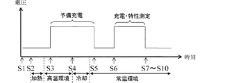
次に、本発明の第3の実施形態に係るセラミックコンデンサの特性測定方法について説明する。図6は、本実施形態に係る特性測定方法のプロセスフローの一例を示すフローチャートである。図7は、本実施形態に係る特性測定方法を実施する特性測定装置の概略構成を示す図である。
<< Third Embodiment >>
Next, a method for measuring the characteristics of a ceramic capacitor according to a third embodiment of the present invention will be described. FIG. 6 is a flowchart showing an example of a process flow of the characteristic measurement method according to the present embodiment. FIG. 7 is a diagram illustrating a schematic configuration of a characteristic measuring apparatus that performs the characteristic measuring method according to the present embodiment.
まず、本実施形態のプロセスフローについて図6に基づいて説明する。本実施形態ではセラミックコンデンサを特性測定装置に供給し(S11)、その特性測定装置で、セラミックコンデンサを加熱(S12)する。そして、セラミックコンデンサの外部端子に接触端子を当接させて電圧を印加し、予備充電(S13)を実施する。 First, the process flow of this embodiment is demonstrated based on FIG. In this embodiment, the ceramic capacitor is supplied to the characteristic measuring device (S11), and the ceramic capacitor is heated (S12) by the characteristic measuring device. And a contact terminal is made to contact | abut to the external terminal of a ceramic capacitor, a voltage is applied, and preliminary charge (S13) is implemented.
そして、同特性測定装置で、セラミックコンデンサの外部端子に電圧を印加していた接触端子を引き離し、両方の外部端子間を開放状態とする。これにより、セラミックコンデンサ自体の蓄積電荷のみによって強誘電体に電界が働く状態としてから、セラミックコンデンサを冷却する(S14)。この場合にも、上記電界に沿った分極方向で自発分極が再生することになり、強誘電体の分極が大幅に進展したものになる。 And the contact terminal which applied the voltage to the external terminal of the ceramic capacitor with the same characteristic measuring apparatus is pulled apart, and both external terminals are opened. As a result, the ceramic capacitor is cooled after the electric field is applied to the ferroelectric substance only by the accumulated charge of the ceramic capacitor itself (S14). Also in this case, the spontaneous polarization is regenerated in the polarization direction along the electric field, and the polarization of the ferroelectric material is greatly advanced.
その後、冷却後のセラミックコンデンサの放電を行い(S15)、測定電圧を印加してセラミックコンデンサを再充電させ(S16)、所定時間の経過後に充電電流値を測定する(S17〜S18)。そして、セラミックコンデンサの良否判定を行い、判定結果に応じた選別・排出を行う(S19〜S21)。 Thereafter, the cooled ceramic capacitor is discharged (S15), the measurement voltage is applied to recharge the ceramic capacitor (S16), and the charging current value is measured after a predetermined time (S17 to S18). And the quality determination of a ceramic capacitor is performed, and selection and discharge according to the determination result are performed (S19 to S21).
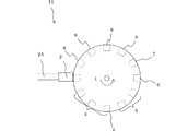
以上のプロセスフローは、図7に示す構成の特性測定装置により実施する。 The above process flow is performed by the characteristic measuring apparatus having the configuration shown in FIG.
特性測定装置11は、セラミックコンデンサの搬送路となる円形テーブル1、振動フィーダ2A、分離供給部2、加熱部3、予備充電部4、冷却部5、放電部6、再充電・特性測定部7、および、排出部8を備える。円形テーブル1は、セラミックコンデンサを保持するためのワーク収納孔が等間隔で形成され、セラミックコンデンサを逆時計回りに間欠搬送する。振動フィーダ2Aは、セラミックコンデンサを分離供給部2まで送る。分離供給部2は、供給位置に位置する円形テーブル1のワーク収納孔にセラミックコンデンサを収納する。加熱部3は、供給位置の次にセラミックコンデンサが搬送される加熱領域でセラミックコンデンサを加熱する。予備充電部4は、加熱領域の最後にセラミックコンデンサが搬送される予備充電位置でセラミックコンデンサを予備充電する。冷却部5は、予備充電位置の次にセラミックコンデンサが搬送される冷却領域でセラミックコンデンサを冷却する。放電部6は、冷却領域の次にセラミックコンデンサが搬送される放電位置でセラミックコンデンサを放電する。再充電・特性測定部7は、放電位置の次にセラミックコンデンサが搬送される再充電・特性測定位置でセラミックコンデンサを再充電して充電電流値を測定する。排出部8は、セラミックコンデンサを特性測定結果に応じた位置から排出する。
The characteristic measuring device 11 includes a circular table 1 serving as a conveyance path for a ceramic capacitor, a
この特性測定装置11では、セラミックコンデンサを間欠送りし、セラミックコンデンサの送り位置ごとに、前述のプロセスフローに示した処理を順次実施する。このような特性測定装置11の詳細構成については特開2009-244116号公報などに公開されているため、ここでの詳述は避けるが、この装置では、予備充電部4によりセラミックコンデンサを予備充電した後で、セラミックコンデンサから電圧印加用の接触端子を引き離し、その後でセラミックコンデンサを冷却部5や放電部6に搬送することになる。このため、この装置を用いれば、各プロセスを同一の送り位置で実施するのではなく別々の送り位置で並列して実施でき、予備充電から冷却、放電までの一連のプロセスを実施するための時間を短縮することができる。そして、そのようにしても、予備充電部4で充電したセラミックコンデンサの放電を、冷却部5での冷却後に実施できるため、強誘電体の分極がキュリー温度以上で消滅することがなく、強誘電体の分極を進行させた状態で、後の再分極および特性測定を実施することができる。
In this characteristic measuring apparatus 11, the ceramic capacitor is intermittently fed, and the processing shown in the above-described process flow is sequentially performed for each ceramic capacitor feeding position. Since the detailed configuration of such a characteristic measuring apparatus 11 is disclosed in Japanese Patent Application Laid-Open No. 2009-244116 and the like, a detailed description thereof is avoided, but in this apparatus, the ceramic capacitor is precharged by the precharge unit 4. After that, the contact terminal for voltage application is separated from the ceramic capacitor, and then the ceramic capacitor is transported to the
なお、加熱領域、予備充電位置、冷却領域、放電位置、再充電特性測定位置、排出部を直線状に配置し、セラミックコンデンサを直線方向に搬送させてもよい。搬送方法は吸着ヘッドによる保持であっても、メカニカルチャックであってもよく、間欠搬送に限らず連続搬送でも良い。 In addition, the heating region, the preliminary charging position, the cooling region, the discharging position, the recharging characteristic measurement position, and the discharge unit may be arranged in a straight line, and the ceramic capacitor may be conveyed in the straight direction. The conveyance method may be holding by a suction head or a mechanical chuck, and is not limited to intermittent conveyance but may be continuous conveyance.
上述した各実施形態での測定方法や測定装置の構成は仕様に応じたものであり、本発明の範囲は、上述の実施形態ではなく特許請求の範囲によって示され、本発明の範囲には特許請求の範囲と均等の意味および範囲内での全ての変更が含まれることが意図される。 The configuration of the measurement method and the measurement apparatus in each of the above-described embodiments is in accordance with the specifications, and the scope of the present invention is indicated by the claims, not the above-described embodiments, and the scope of the present invention includes patents. It is intended that all modifications within the meaning and range equivalent to the terms of the claims are included.
1…円形テーブル
2…分離供給部
2A…振動フィーダ
3…加熱部
4…予備充電部
5…冷却部
6…放電部
7…特性測定部
8…排出部
11…特性測定装置
DESCRIPTION OF
Claims (5)
キュリー温度以上に加熱した前記容量素子に電圧印加して予備充電する予備充電ステップと、
予備充電の途中または予備充電の終了後に前記容量素子をキュリー温度未満に冷却する冷却ステップと、
キュリー温度未満に冷却した前記容量素子を放電する放電ステップと、
放電後の前記容量素子に電圧印加し再充電して特性を測定する再充電・特性測定ステップと、
を有する容量素子の特性測定方法。 A heating step of heating the capacitive element made of a ferroelectric material to a temperature above the Curie temperature;
A preliminary charging step of applying a voltage to the capacitive element heated to a temperature above the Curie temperature to perform preliminary charging;
A cooling step for cooling the capacitive element to less than the Curie temperature in the middle of the precharge or after the end of the precharge;
A discharging step of discharging the capacitive element cooled to a temperature lower than the Curie temperature;
A recharging / characteristic measuring step for measuring the characteristics by applying a voltage to the capacitive element after discharging and recharging,
The characteristic measuring method of the capacitive element which has this.
前記容量素子を供給位置から排出位置まで搬送する搬送路を備え、
前記搬送路には、
前記容量素子をキュリー温度以上に加熱する加熱領域、
前記加熱領域で加熱された容量素子に電圧印加して予備充電する予備充電位置、
前記予備充電位置で充電された前記容量素子をキュリー温度未満に冷却する冷却領域、
前記冷却領域で冷却された前記容量素子中の電荷を放電する放電位置、
前記放電位置で放電された前記容量素子に電圧印加し再充電して特性を測定する再充電・特性測定位置、が順に配置されていることを特徴とする、特性測定装置。 A characteristic measuring device for measuring characteristics of a plurality of capacitive elements made of a ferroelectric material,
A transport path for transporting the capacitive element from a supply position to a discharge position;
In the conveyance path,
A heating region for heating the capacitive element to a Curie temperature or higher;
A precharging position for precharging by applying a voltage to the capacitive element heated in the heating region,
A cooling region for cooling the capacitive element charged at the preliminary charging position to less than the Curie temperature;
A discharge position for discharging the charge in the capacitive element cooled in the cooling region;
A characteristic measurement device in which recharge / characteristic measurement positions for measuring characteristics by applying a voltage to the capacitor element discharged at the discharge position and recharging are arranged in order.
Priority Applications (1)
| Application Number | Priority Date | Filing Date | Title |
|---|---|---|---|
| JP2010275204A JP5522012B2 (en) | 2010-12-10 | 2010-12-10 | Capacitance element characteristic measuring method and characteristic measuring apparatus |
Applications Claiming Priority (1)
| Application Number | Priority Date | Filing Date | Title |
|---|---|---|---|
| JP2010275204A JP5522012B2 (en) | 2010-12-10 | 2010-12-10 | Capacitance element characteristic measuring method and characteristic measuring apparatus |
Publications (2)
| Publication Number | Publication Date |
|---|---|
| JP2012122910A JP2012122910A (en) | 2012-06-28 |
| JP5522012B2 true JP5522012B2 (en) | 2014-06-18 |
Family
ID=46504486
Family Applications (1)
| Application Number | Title | Priority Date | Filing Date |
|---|---|---|---|
| JP2010275204A Active JP5522012B2 (en) | 2010-12-10 | 2010-12-10 | Capacitance element characteristic measuring method and characteristic measuring apparatus |
Country Status (1)
| Country | Link |
|---|---|
| JP (1) | JP5522012B2 (en) |
Cited By (1)
| Publication number | Priority date | Publication date | Assignee | Title |
|---|---|---|---|---|
| CN110687467A (en) * | 2019-11-13 | 2020-01-14 | 珠海冠宇电池有限公司 | Method for detecting leakage current of lithium battery |
Families Citing this family (3)
| Publication number | Priority date | Publication date | Assignee | Title |
|---|---|---|---|---|
| KR102881741B1 (en) | 2019-09-09 | 2025-11-04 | 삼성전자주식회사 | Memory device including path circuit, and memory system thererof |
| JP7449581B2 (en) * | 2021-06-28 | 2024-03-14 | 株式会社 東京ウエルズ | Capacitor measuring device and capacitor measuring method |
| JP2024175949A (en) * | 2023-06-07 | 2024-12-19 | 株式会社 東京ウエルズ | Inspection device and inspection method |
-
2010
- 2010-12-10 JP JP2010275204A patent/JP5522012B2/en active Active
Cited By (1)
| Publication number | Priority date | Publication date | Assignee | Title |
|---|---|---|---|---|
| CN110687467A (en) * | 2019-11-13 | 2020-01-14 | 珠海冠宇电池有限公司 | Method for detecting leakage current of lithium battery |
Also Published As
| Publication number | Publication date |
|---|---|
| JP2012122910A (en) | 2012-06-28 |
Similar Documents
| Publication | Publication Date | Title |
|---|---|---|
| JP5522012B2 (en) | Capacitance element characteristic measuring method and characteristic measuring apparatus | |
| CN101587813B (en) | Stage mechanism, plasma processing apparatus and voltage application method | |
| JP5218823B2 (en) | Capacitor leakage current measuring method and capacitor leakage current measuring apparatus | |
| TWI687021B (en) | Adaptive battery charging method, charging device, computer program and computer readable storage medium | |
| AU2019332984A1 (en) | Apparatus for an aerosol generating device | |
| US8351166B2 (en) | Leakage sensor and switch device for deep-trench capacitor array | |
| US9041413B2 (en) | Electric leakage detection apparatus | |
| JPS6244410B2 (en) | ||
| CN105556792A (en) | Power storage device, power storage control device, and power storage control method | |
| CN112213650A (en) | Inspection method and manufacturing method of electrical storage device | |
| JP2025011336A (en) | Method and system for induction heating | |
| JP7449581B2 (en) | Capacitor measuring device and capacitor measuring method | |
| TW591674B (en) | Method of processing a ceramic capacitor | |
| TWI605004B (en) | Electronic component transporting device | |
| JP7353910B2 (en) | Tool battery pack charger, charging method and program | |
| CN103558475B (en) | A kind of method for detection of ferroelectric ceramics energy storage characteristic | |
| Manceau et al. | Leakage current variation with time in Ta2O5 MIM and MIS capacitors | |
| JP2002222850A (en) | Detachment method of adsorbed object in electrostatic chuck | |
| Maur et al. | Investigation on Effects of Thermal Ageing on LDPE Based on Polarization and Depolarization Currents | |
| JP2024175949A (en) | Inspection device and inspection method | |
| JP2002260974A (en) | Leakage current inspection device for electrolytic capacitors | |
| TWI843824B (en) | Electrostatic adsorption device and static removal method | |
| JP2002151368A (en) | Method for manufacturing and measuring capacitor | |
| JP2004077238A (en) | Characteristic measuring device of electronic component | |
| JP2004177169A (en) | Measuring apparatus for capacitor characteristics |
Legal Events
| Date | Code | Title | Description |
|---|---|---|---|
| A621 | Written request for application examination |
Free format text: JAPANESE INTERMEDIATE CODE: A621 Effective date: 20130918 |
|
| A977 | Report on retrieval |
Free format text: JAPANESE INTERMEDIATE CODE: A971007 Effective date: 20140207 |
|
| TRDD | Decision of grant or rejection written | ||
| A01 | Written decision to grant a patent or to grant a registration (utility model) |
Free format text: JAPANESE INTERMEDIATE CODE: A01 Effective date: 20140311 |
|
| A61 | First payment of annual fees (during grant procedure) |
Free format text: JAPANESE INTERMEDIATE CODE: A61 Effective date: 20140324 |
|
| R150 | Certificate of patent or registration of utility model |
Ref document number: 5522012 Country of ref document: JP Free format text: JAPANESE INTERMEDIATE CODE: R150 |