JP5489717B2 - Method and integrated system for conditioning a substrate surface for metal deposition - Google Patents
Method and integrated system for conditioning a substrate surface for metal deposition Download PDFInfo
- Publication number
- JP5489717B2 JP5489717B2 JP2009526621A JP2009526621A JP5489717B2 JP 5489717 B2 JP5489717 B2 JP 5489717B2 JP 2009526621 A JP2009526621 A JP 2009526621A JP 2009526621 A JP2009526621 A JP 2009526621A JP 5489717 B2 JP5489717 B2 JP 5489717B2
- Authority
- JP
- Japan
- Prior art keywords
- copper
- substrate
- integrated system
- metal
- vacuum
- Prior art date
- Legal status (The legal status is an assumption and is not a legal conclusion. Google has not performed a legal analysis and makes no representation as to the accuracy of the status listed.)
- Expired - Fee Related
Links
- 238000000034 method Methods 0.000 title claims description 588
- 239000000758 substrate Substances 0.000 title claims description 401
- 230000003750 conditioning effect Effects 0.000 title description 34
- 238000001465 metallisation Methods 0.000 title description 10
- 230000008569 process Effects 0.000 claims description 486
- 239000010949 copper Substances 0.000 claims description 399
- RYGMFSIKBFXOCR-UHFFFAOYSA-N Copper Chemical compound [Cu] RYGMFSIKBFXOCR-UHFFFAOYSA-N 0.000 claims description 392
- 229910052802 copper Inorganic materials 0.000 claims description 389
- 238000012546 transfer Methods 0.000 claims description 243
- 230000004888 barrier function Effects 0.000 claims description 240
- 229910052751 metal Inorganic materials 0.000 claims description 231
- 239000002184 metal Substances 0.000 claims description 231
- 238000000151 deposition Methods 0.000 claims description 197
- 230000008021 deposition Effects 0.000 claims description 144
- 238000004140 cleaning Methods 0.000 claims description 127
- 229910000531 Co alloy Inorganic materials 0.000 claims description 119
- 239000000356 contaminant Substances 0.000 claims description 94
- 238000004320 controlled atmosphere Methods 0.000 claims description 93
- QVGXLLKOCUKJST-UHFFFAOYSA-N atomic oxygen Chemical compound [O] QVGXLLKOCUKJST-UHFFFAOYSA-N 0.000 claims description 85
- 239000001301 oxygen Substances 0.000 claims description 85
- 229910052760 oxygen Inorganic materials 0.000 claims description 85
- 239000012298 atmosphere Substances 0.000 claims description 75
- 239000011261 inert gas Substances 0.000 claims description 62
- 150000004706 metal oxides Chemical class 0.000 claims description 57
- 239000001257 hydrogen Substances 0.000 claims description 55
- 229910052739 hydrogen Inorganic materials 0.000 claims description 55
- 229910044991 metal oxide Inorganic materials 0.000 claims description 54
- QPLDLSVMHZLSFG-UHFFFAOYSA-N Copper oxide Chemical compound [Cu]=O QPLDLSVMHZLSFG-UHFFFAOYSA-N 0.000 claims description 52
- UFHFLCQGNIYNRP-UHFFFAOYSA-N Hydrogen Chemical compound [H][H] UFHFLCQGNIYNRP-UHFFFAOYSA-N 0.000 claims description 50
- 238000012545 processing Methods 0.000 claims description 50
- 239000005751 Copper oxide Substances 0.000 claims description 48
- 229910000431 copper oxide Inorganic materials 0.000 claims description 48
- 230000009467 reduction Effects 0.000 claims description 39
- 238000005137 deposition process Methods 0.000 claims description 32
- 239000000956 alloy Substances 0.000 claims description 26
- KRKNYBCHXYNGOX-UHFFFAOYSA-N citric acid Chemical compound OC(=O)CC(O)(C(O)=O)CC(O)=O KRKNYBCHXYNGOX-UHFFFAOYSA-N 0.000 claims description 21
- 238000011946 reduction process Methods 0.000 claims description 21
- 239000007789 gas Substances 0.000 claims description 17
- 238000005530 etching Methods 0.000 claims description 14
- 239000012530 fluid Substances 0.000 claims description 13
- 239000000203 mixture Substances 0.000 claims description 13
- QGZKDVFQNNGYKY-UHFFFAOYSA-N Ammonia Chemical compound N QGZKDVFQNNGYKY-UHFFFAOYSA-N 0.000 claims description 10
- MHAJPDPJQMAIIY-UHFFFAOYSA-N Hydrogen peroxide Chemical compound OO MHAJPDPJQMAIIY-UHFFFAOYSA-N 0.000 claims description 8
- QAOWNCQODCNURD-UHFFFAOYSA-N Sulfuric acid Chemical compound OS(O)(=O)=O QAOWNCQODCNURD-UHFFFAOYSA-N 0.000 claims description 8
- 229910021529 ammonia Inorganic materials 0.000 claims description 5
- 150000002431 hydrogen Chemical class 0.000 claims description 5
- 238000006243 chemical reaction Methods 0.000 claims description 4
- 238000004043 dyeing Methods 0.000 claims 1
- PCHJSUWPFVWCPO-UHFFFAOYSA-N gold Chemical compound [Au] PCHJSUWPFVWCPO-UHFFFAOYSA-N 0.000 claims 1
- 239000010931 gold Substances 0.000 claims 1
- 229910052737 gold Inorganic materials 0.000 claims 1
- 239000010410 layer Substances 0.000 description 334
- XUIMIQQOPSSXEZ-UHFFFAOYSA-N Silicon Chemical compound [Si] XUIMIQQOPSSXEZ-UHFFFAOYSA-N 0.000 description 51
- 229910052710 silicon Inorganic materials 0.000 description 48
- 239000010703 silicon Substances 0.000 description 48
- 238000004544 sputter deposition Methods 0.000 description 33
- MZLGASXMSKOWSE-UHFFFAOYSA-N tantalum nitride Chemical compound [Ta]#N MZLGASXMSKOWSE-UHFFFAOYSA-N 0.000 description 30
- 239000000126 substance Substances 0.000 description 29
- 239000010408 film Substances 0.000 description 28
- 229910021332 silicide Inorganic materials 0.000 description 27
- 239000000463 material Substances 0.000 description 26
- 238000010586 diagram Methods 0.000 description 25
- 238000011049 filling Methods 0.000 description 25
- FVBUAEGBCNSCDD-UHFFFAOYSA-N silicide(4-) Chemical compound [Si-4] FVBUAEGBCNSCDD-UHFFFAOYSA-N 0.000 description 25
- 238000000231 atomic layer deposition Methods 0.000 description 22
- 229910021420 polycrystalline silicon Inorganic materials 0.000 description 21
- 229920005591 polysilicon Polymers 0.000 description 21
- 230000015572 biosynthetic process Effects 0.000 description 20
- 238000005240 physical vapour deposition Methods 0.000 description 20
- VYPSYNLAJGMNEJ-UHFFFAOYSA-N Silicium dioxide Chemical compound O=[Si]=O VYPSYNLAJGMNEJ-UHFFFAOYSA-N 0.000 description 18
- 238000007747 plating Methods 0.000 description 18
- 238000009713 electroplating Methods 0.000 description 17
- HBMJWWWQQXIZIP-UHFFFAOYSA-N silicon carbide Chemical compound [Si+]#[C-] HBMJWWWQQXIZIP-UHFFFAOYSA-N 0.000 description 17
- WGTYBPLFGIVFAS-UHFFFAOYSA-M tetramethylammonium hydroxide Chemical compound [OH-].C[N+](C)(C)C WGTYBPLFGIVFAS-UHFFFAOYSA-M 0.000 description 16
- 238000001035 drying Methods 0.000 description 14
- 229910010271 silicon carbide Inorganic materials 0.000 description 14
- 238000000454 electroless metal deposition Methods 0.000 description 12
- 239000003989 dielectric material Substances 0.000 description 11
- 230000001419 dependent effect Effects 0.000 description 10
- 230000009977 dual effect Effects 0.000 description 10
- 229910052715 tantalum Inorganic materials 0.000 description 10
- 239000012964 benzotriazole Substances 0.000 description 9
- -1 copper-BTA complexes Chemical class 0.000 description 9
- 230000003647 oxidation Effects 0.000 description 9
- 238000007254 oxidation reaction Methods 0.000 description 9
- GUVRBAGPIYLISA-UHFFFAOYSA-N tantalum atom Chemical compound [Ta] GUVRBAGPIYLISA-UHFFFAOYSA-N 0.000 description 9
- 235000012431 wafers Nutrition 0.000 description 9
- 238000003631 wet chemical etching Methods 0.000 description 9
- QRUDEWIWKLJBPS-UHFFFAOYSA-N benzotriazole Chemical compound C1=CC=C2N[N][N]C2=C1 QRUDEWIWKLJBPS-UHFFFAOYSA-N 0.000 description 8
- 230000000694 effects Effects 0.000 description 8
- 150000007524 organic acids Chemical class 0.000 description 8
- 238000009832 plasma treatment Methods 0.000 description 8
- 239000004065 semiconductor Substances 0.000 description 8
- 229910052814 silicon oxide Inorganic materials 0.000 description 8
- 238000004381 surface treatment Methods 0.000 description 8
- 230000003197 catalytic effect Effects 0.000 description 7
- 230000001737 promoting effect Effects 0.000 description 7
- UGFAIRIUMAVXCW-UHFFFAOYSA-N Carbon monoxide Chemical compound [O+]#[C-] UGFAIRIUMAVXCW-UHFFFAOYSA-N 0.000 description 6
- PXHVJJICTQNCMI-UHFFFAOYSA-N Nickel Chemical compound [Ni] PXHVJJICTQNCMI-UHFFFAOYSA-N 0.000 description 6
- 229910052581 Si3N4 Inorganic materials 0.000 description 6
- 229910002091 carbon monoxide Inorganic materials 0.000 description 6
- 239000003638 chemical reducing agent Substances 0.000 description 6
- 238000005516 engineering process Methods 0.000 description 6
- HQVNEWCFYHHQES-UHFFFAOYSA-N silicon nitride Chemical compound N12[Si]34N5[Si]62N3[Si]51N64 HQVNEWCFYHHQES-UHFFFAOYSA-N 0.000 description 6
- WFKWXMTUELFFGS-UHFFFAOYSA-N tungsten Chemical compound [W] WFKWXMTUELFFGS-UHFFFAOYSA-N 0.000 description 6
- 229910052721 tungsten Inorganic materials 0.000 description 6
- 239000010937 tungsten Substances 0.000 description 6
- 230000000536 complexating effect Effects 0.000 description 5
- 238000007872 degassing Methods 0.000 description 5
- 238000009792 diffusion process Methods 0.000 description 5
- 238000007772 electroless plating Methods 0.000 description 5
- 230000010354 integration Effects 0.000 description 5
- 235000005985 organic acids Nutrition 0.000 description 5
- 230000001590 oxidative effect Effects 0.000 description 5
- 229910052707 ruthenium Inorganic materials 0.000 description 5
- XKRFYHLGVUSROY-UHFFFAOYSA-N Argon Chemical compound [Ar] XKRFYHLGVUSROY-UHFFFAOYSA-N 0.000 description 4
- ZOXJGFHDIHLPTG-UHFFFAOYSA-N Boron Chemical compound [B] ZOXJGFHDIHLPTG-UHFFFAOYSA-N 0.000 description 4
- PIICEJLVQHRZGT-UHFFFAOYSA-N Ethylenediamine Chemical compound NCCN PIICEJLVQHRZGT-UHFFFAOYSA-N 0.000 description 4
- OAICVXFJPJFONN-UHFFFAOYSA-N Phosphorus Chemical compound [P] OAICVXFJPJFONN-UHFFFAOYSA-N 0.000 description 4
- KJTLSVCANCCWHF-UHFFFAOYSA-N Ruthenium Chemical compound [Ru] KJTLSVCANCCWHF-UHFFFAOYSA-N 0.000 description 4
- 239000002253 acid Substances 0.000 description 4
- 150000007513 acids Chemical class 0.000 description 4
- 150000001412 amines Chemical class 0.000 description 4
- 229910052796 boron Inorganic materials 0.000 description 4
- 239000004020 conductor Substances 0.000 description 4
- 238000013461 design Methods 0.000 description 4
- 239000010432 diamond Substances 0.000 description 4
- 238000002955 isolation Methods 0.000 description 4
- 229910052759 nickel Inorganic materials 0.000 description 4
- BPUBBGLMJRNUCC-UHFFFAOYSA-N oxygen(2-);tantalum(5+) Chemical compound [O-2].[O-2].[O-2].[O-2].[O-2].[Ta+5].[Ta+5] BPUBBGLMJRNUCC-UHFFFAOYSA-N 0.000 description 4
- 238000000059 patterning Methods 0.000 description 4
- 229910052698 phosphorus Inorganic materials 0.000 description 4
- 239000011574 phosphorus Substances 0.000 description 4
- 239000000377 silicon dioxide Substances 0.000 description 4
- 235000012239 silicon dioxide Nutrition 0.000 description 4
- 229910001936 tantalum oxide Inorganic materials 0.000 description 4
- RPNUMPOLZDHAAY-UHFFFAOYSA-N Diethylenetriamine Chemical compound NCCNCCN RPNUMPOLZDHAAY-UHFFFAOYSA-N 0.000 description 3
- AVXURJPOCDRRFD-UHFFFAOYSA-N Hydroxylamine Chemical compound ON AVXURJPOCDRRFD-UHFFFAOYSA-N 0.000 description 3
- CBENFWSGALASAD-UHFFFAOYSA-N Ozone Chemical compound [O-][O+]=O CBENFWSGALASAD-UHFFFAOYSA-N 0.000 description 3
- 238000007792 addition Methods 0.000 description 3
- 238000011109 contamination Methods 0.000 description 3
- 238000005429 filling process Methods 0.000 description 3
- QAMFBRUWYYMMGJ-UHFFFAOYSA-N hexafluoroacetylacetone Chemical compound FC(F)(F)C(=O)CC(=O)C(F)(F)F QAMFBRUWYYMMGJ-UHFFFAOYSA-N 0.000 description 3
- 150000007522 mineralic acids Chemical class 0.000 description 3
- QGLKJKCYBOYXKC-UHFFFAOYSA-N nonaoxidotritungsten Chemical compound O=[W]1(=O)O[W](=O)(=O)O[W](=O)(=O)O1 QGLKJKCYBOYXKC-UHFFFAOYSA-N 0.000 description 3
- 150000002978 peroxides Chemical class 0.000 description 3
- 238000001020 plasma etching Methods 0.000 description 3
- 239000002356 single layer Substances 0.000 description 3
- 239000010936 titanium Substances 0.000 description 3
- 229910001930 tungsten oxide Inorganic materials 0.000 description 3
- IJGRMHOSHXDMSA-UHFFFAOYSA-N Atomic nitrogen Chemical compound N#N IJGRMHOSHXDMSA-UHFFFAOYSA-N 0.000 description 2
- YCKRFDGAMUMZLT-UHFFFAOYSA-N Fluorine atom Chemical compound [F] YCKRFDGAMUMZLT-UHFFFAOYSA-N 0.000 description 2
- BOTDANWDWHJENH-UHFFFAOYSA-N Tetraethyl orthosilicate Chemical compound CCO[Si](OCC)(OCC)OCC BOTDANWDWHJENH-UHFFFAOYSA-N 0.000 description 2
- FEBFYWHXKVOHDI-UHFFFAOYSA-N [Co].[P][W] Chemical compound [Co].[P][W] FEBFYWHXKVOHDI-UHFFFAOYSA-N 0.000 description 2
- 229910052782 aluminium Inorganic materials 0.000 description 2
- XAGFODPZIPBFFR-UHFFFAOYSA-N aluminium Chemical compound [Al] XAGFODPZIPBFFR-UHFFFAOYSA-N 0.000 description 2
- 229910052786 argon Inorganic materials 0.000 description 2
- 125000004429 atom Chemical group 0.000 description 2
- 230000008901 benefit Effects 0.000 description 2
- 239000013043 chemical agent Substances 0.000 description 2
- 239000010941 cobalt Substances 0.000 description 2
- 229910017052 cobalt Inorganic materials 0.000 description 2
- GUTLYIVDDKVIGB-UHFFFAOYSA-N cobalt atom Chemical compound [Co] GUTLYIVDDKVIGB-UHFFFAOYSA-N 0.000 description 2
- 230000001143 conditioned effect Effects 0.000 description 2
- 230000007797 corrosion Effects 0.000 description 2
- 238000005260 corrosion Methods 0.000 description 2
- 230000007613 environmental effect Effects 0.000 description 2
- 239000011737 fluorine Substances 0.000 description 2
- 229910052731 fluorine Inorganic materials 0.000 description 2
- 239000001307 helium Substances 0.000 description 2
- 229910052734 helium Inorganic materials 0.000 description 2
- SWQJXJOGLNCZEY-UHFFFAOYSA-N helium atom Chemical compound [He] SWQJXJOGLNCZEY-UHFFFAOYSA-N 0.000 description 2
- 238000011534 incubation Methods 0.000 description 2
- 229910052743 krypton Inorganic materials 0.000 description 2
- DNNSSWSSYDEUBZ-UHFFFAOYSA-N krypton atom Chemical compound [Kr] DNNSSWSSYDEUBZ-UHFFFAOYSA-N 0.000 description 2
- 239000007788 liquid Substances 0.000 description 2
- 150000002739 metals Chemical class 0.000 description 2
- 229910052754 neon Inorganic materials 0.000 description 2
- GKAOGPIIYCISHV-UHFFFAOYSA-N neon atom Chemical compound [Ne] GKAOGPIIYCISHV-UHFFFAOYSA-N 0.000 description 2
- 230000006911 nucleation Effects 0.000 description 2
- 238000010899 nucleation Methods 0.000 description 2
- 125000002524 organometallic group Chemical group 0.000 description 2
- 238000002161 passivation Methods 0.000 description 2
- 238000000623 plasma-assisted chemical vapour deposition Methods 0.000 description 2
- 238000005498 polishing Methods 0.000 description 2
- 239000002243 precursor Substances 0.000 description 2
- 229910001925 ruthenium oxide Inorganic materials 0.000 description 2
- WOCIAKWEIIZHES-UHFFFAOYSA-N ruthenium(iv) oxide Chemical compound O=[Ru]=O WOCIAKWEIIZHES-UHFFFAOYSA-N 0.000 description 2
- 239000007787 solid Substances 0.000 description 2
- 238000006467 substitution reaction Methods 0.000 description 2
- 239000010409 thin film Substances 0.000 description 2
- 229910052719 titanium Inorganic materials 0.000 description 2
- 239000011800 void material Substances 0.000 description 2
- 238000007704 wet chemistry method Methods 0.000 description 2
- 229910052724 xenon Inorganic materials 0.000 description 2
- FHNFHKCVQCLJFQ-UHFFFAOYSA-N xenon atom Chemical compound [Xe] FHNFHKCVQCLJFQ-UHFFFAOYSA-N 0.000 description 2
- 229910000838 Al alloy Inorganic materials 0.000 description 1
- OKTJSMMVPCPJKN-UHFFFAOYSA-N Carbon Chemical compound [C] OKTJSMMVPCPJKN-UHFFFAOYSA-N 0.000 description 1
- 244000132059 Carica parviflora Species 0.000 description 1
- 235000014653 Carica parviflora Nutrition 0.000 description 1
- OKIZCWYLBDKLSU-UHFFFAOYSA-M N,N,N-Trimethylmethanaminium chloride Chemical compound [Cl-].C[N+](C)(C)C OKIZCWYLBDKLSU-UHFFFAOYSA-M 0.000 description 1
- 241000233805 Phoenix Species 0.000 description 1
- RTAQQCXQSZGOHL-UHFFFAOYSA-N Titanium Chemical compound [Ti] RTAQQCXQSZGOHL-UHFFFAOYSA-N 0.000 description 1
- CPJYFACXEHYLFS-UHFFFAOYSA-N [B].[W].[Co] Chemical compound [B].[W].[Co] CPJYFACXEHYLFS-UHFFFAOYSA-N 0.000 description 1
- 230000002378 acidificating effect Effects 0.000 description 1
- 230000002411 adverse Effects 0.000 description 1
- 239000003125 aqueous solvent Substances 0.000 description 1
- 239000005441 aurora Substances 0.000 description 1
- RJTANRZEWTUVMA-UHFFFAOYSA-N boron;n-methylmethanamine Chemical compound [B].CNC RJTANRZEWTUVMA-UHFFFAOYSA-N 0.000 description 1
- 239000003990 capacitor Substances 0.000 description 1
- 229910052799 carbon Inorganic materials 0.000 description 1
- 239000003054 catalyst Substances 0.000 description 1
- 238000004891 communication Methods 0.000 description 1
- 150000001875 compounds Chemical class 0.000 description 1
- 150000001880 copper compounds Chemical group 0.000 description 1
- 230000007547 defect Effects 0.000 description 1
- 239000002019 doping agent Substances 0.000 description 1
- 239000011521 glass Substances 0.000 description 1
- 239000008241 heterogeneous mixture Substances 0.000 description 1
- 238000007654 immersion Methods 0.000 description 1
- 238000011065 in-situ storage Methods 0.000 description 1
- 238000010348 incorporation Methods 0.000 description 1
- 239000003112 inhibitor Substances 0.000 description 1
- 230000000977 initiatory effect Effects 0.000 description 1
- 238000004519 manufacturing process Methods 0.000 description 1
- 239000012528 membrane Substances 0.000 description 1
- 229910021471 metal-silicon alloy Inorganic materials 0.000 description 1
- 230000005012 migration Effects 0.000 description 1
- 238000013508 migration Methods 0.000 description 1
- 238000002156 mixing Methods 0.000 description 1
- 150000004767 nitrides Chemical class 0.000 description 1
- 150000007530 organic bases Chemical class 0.000 description 1
- 239000011368 organic material Substances 0.000 description 1
- 239000002245 particle Substances 0.000 description 1
- ACVYVLVWPXVTIT-UHFFFAOYSA-M phosphinate Chemical compound [O-][PH2]=O ACVYVLVWPXVTIT-UHFFFAOYSA-M 0.000 description 1
- 229920002120 photoresistant polymer Polymers 0.000 description 1
- 230000002028 premature Effects 0.000 description 1
- 238000010926 purge Methods 0.000 description 1
- 239000000376 reactant Substances 0.000 description 1
- 238000005201 scrubbing Methods 0.000 description 1
- 125000006850 spacer group Chemical group 0.000 description 1
- 241000894007 species Species 0.000 description 1
- 230000007704 transition Effects 0.000 description 1
- XLYOFNOQVPJJNP-UHFFFAOYSA-N water Chemical compound O XLYOFNOQVPJJNP-UHFFFAOYSA-N 0.000 description 1
Images


Description
集積回路は、半導体基板上の個々の素子をつなぐためまたは集積回路に対して対外的に通信するために、導電性の配線を使用する。ビアおよびトレンチのための配線メタライゼーションは、アルミニウム合金および銅を含んでよい。エレクトロマイグレーション(EM)は、金属配線についてよく知られた信頼性の問題であり、電流密度によって決定される速度で電子が電流の方向に金属原子を押し動かすことによって引き起こされる。エレクトロマイグレーションは、最終的には金属線の細線化につながる恐れがあり、これは、結果として、抵抗率の増大、あるいは最悪の場合は金属線の破損を生じる恐れがある。幸いなことに、IC上の配線金属線は、その全てにおいて常に同じ方向に電流が流れているわけではなく、電源ラインおよびアースラインにおいてほぼそうであるのとは異なる。しかしながら、金属線が狭くなるにつれ(国際半導体技術ロードマップ(International Technology Roadmap for Semiconductors (ITRS)は、技術ノードごとに〜0.7倍の線幅縮小を呼びかけている)、エレクトロマイグレーションは、ますます問題になっている。 Integrated circuits use conductive wiring to connect individual elements on a semiconductor substrate or to communicate externally to the integrated circuit. Wiring metallization for vias and trenches may include aluminum alloys and copper. Electromigration (EM) is a well-known reliability issue for metal interconnects and is caused by electrons moving metal atoms in the direction of current at a rate determined by the current density. Electromigration can ultimately lead to thinning of the metal wire, which can result in increased resistivity or, in the worst case, damage to the metal wire. Fortunately, all of the wiring metal lines on the IC do not always have current flowing in the same direction, unlike the power line and ground lines. However, as metal lines become narrower (International Technology Roadmap for Semiconductors (ITRS) calls for ~ 0.7x linewidth reduction per technology node), electromigration is increasingly It is a problem.
アルミニウム線において、EMは、バルク現象であり、銅などの少量のドーパントの添加によって上手く制御される。他方、銅線におけるEMは、表面現象である。これは、銅が自由に移動することができるあらゆる場所において生じる可能性があり、一般に、銅と別の材料との接着に乏しい界面において生じる。今日のデュアルダマシンプロセスでは、これは、通常SiC拡散バリア層である層と境を接する銅線上部において最も頻繁に発生するが、銅/バリア界面においても発生する恐れがある。次の技術ノードへの移行ごとに、そしてその結果としての電流密度の増大とともに、問題は悪化する。 In aluminum wires, EM is a bulk phenomenon and is well controlled by the addition of small amounts of dopants such as copper. On the other hand, EM in copper wire is a surface phenomenon. This can occur anywhere where copper can move freely, and generally occurs at poorly bonded interfaces between copper and another material. In today's dual damascene processes, this occurs most frequently at the top of the copper line bordering the layer, which is typically a SiC diffusion barrier layer, but can also occur at the copper / barrier interface. The problem gets worse with each transition to the next technology node and with the resulting increase in current density.
EMの問題、およびもう1つのよくある信頼性の問題である関連のストレスボイドに対する解決法は、プロセス統合の経緯であった。すなわち、最適化された堆積(すなわちバリアおよびシード層の厚さを低減させるような堆積)、堆積前および堆積後におけるウエハ洗浄、表面処理など、いずれも均質な表面を提供するとともに層間の接着を優れたものにして金属原子の移動およびボイドの伝搬を最小限にすることを狙いとしたプロセスを統合する経緯であった。デュアルダマシンプロセスでは、(コンタクトおよびビアのための)トレンチおよびホールが誘電体内にエッチングされ、次いで、タンタル(Ta)、窒化タンタル(TaN)、または両膜の組み合わせなどのバリア材料で裏打ちされる。次いで、銅シード層の堆積、銅の電解めっき、CMPを使用した銅の平坦化、およびSiC/low−k/SiCなどの誘電体スタックの堆積が続く。銅は、空気に曝露されるとその上に容易に酸化物を形成されるので、銅とSiCとの間に優れた接着を保証するには、銅にSiCを被せる前に適切なCMP後洗浄および酸化銅除去を行う必要がある。SiC堆積に先立つ酸化銅の除去は、優れたEM耐性の実現およびその結果としての金属抵抗率の低減にとって不可欠である。 The solution to the EM problem and the associated stress void, another common reliability problem, was the process integration process. That is, optimized deposition (ie deposition that reduces the thickness of the barrier and seed layers), wafer cleaning before and after deposition, surface treatment, etc. all provide a uniform surface and provide adhesion between layers It was the process of integrating processes aimed at making it excellent and minimizing metal atom migration and void propagation. In the dual damascene process, trenches and holes (for contacts and vias) are etched into the dielectric and then lined with a barrier material such as tantalum (Ta), tantalum nitride (TaN), or a combination of both films. This is followed by copper seed layer deposition, copper electroplating, copper planarization using CMP, and dielectric stack deposition such as SiC / low-k / SiC. Because copper easily forms oxides on it when exposed to air, to ensure good adhesion between copper and SiC, proper post-CMP cleaning before copper is covered with SiC And copper oxide must be removed. Removal of copper oxide prior to SiC deposition is essential for achieving excellent EM resistance and resulting metal resistivity reduction.
近年では、SiC誘電体バリア層の前に、CoWP(コバルト・タングステン・リン)、CoWB(コバルト・タングステン・ホウ素)、またはCoWBP(コバルト・タングステン・リン化ホウ素)などのコバルト合金キャップ層を銅に被せると、銅の上にSiCを設ける場合と比べて大幅にエレクトロマイグレーションが改善されることが示されている。図1は、銅層23,33の上になおかつ誘電体キャップSiC層25,35の下にコバルト合金キャップ層20,30がそれぞれ堆積されたことを示している。層24,34として、Taおよび/TaNのバリア層が例示されている。コバルト合金層20,30は、銅23,33とSiCキャップ層25,35との間の接着を改善する。コバルト合金層20,30は、いくらかの銅拡散バリア特性を呈することもできる。コバルト合金キャップ層は、無電解堆積によって銅上に選択的に堆積させることができる。しかしながら、無電解堆積は、銅が空気に曝露されると形成されえる薄い酸化銅の層によって阻まれる恐れがある。さらに、銅表面上および誘電体表面上の汚染物は、パターン依存性のめっき効果を引き起こす恐れがある。パターン依存性のめっき効果には、パターン依存性のCo合金厚さ、およびCoめっき反応を開始させるために必要とされる「インキュベーション時間」中のエッチングに一部起因するパターン依存性の銅線厚さ喪失などがある。したがって、コバルト合金などの金属キャップ層を堆積させる直前に、処理環境を制御することによって、自然酸化銅の成長を制限(すなわち制御)することならびに銅表面上の酸化銅および有機汚染物と誘電体表面上の有機汚染物および金属汚染物とを除去することが重要である。さらに、パターン依存性の堆積ばらつきを少なくするには、誘電体表面を制御して、それがパターン密度の異なる構造に及ぼす影響を標準化しなければならない。優れた界面接着および優れたEM耐性を保証するには、銅層間23,33、銅−バリア層間33,34および23,24、ならびに接着促進層(すなわち金属キャップ層)とコバルト合金層20,20などとの間の金属−金属界面を設計することが非常に重要である。さらに、金属線が狭くなるにつれ、物理気相成長(PVD)によるバリア膜およびシード膜が金属線に占める部分が大きくなり、これは、実効抵抗率を、ひいては電流密度を増大させる。薄くて共形のバリア層およびシード層は、共形のステップカバレッジおよび許容可能なバリア特性を提供する原子層成長(ALD)バリア(TaN、Ru、または異種混合)と、共形のシード層を提供する無電解Cuプロセスとによって、この傾向を軽減することができる。しかしながら、これまでは、生成されるALD TaNバリア膜に接着することができる無電解Cuシード層がなかった。
In recent years, a cobalt alloy cap layer such as CoWP (Cobalt Tungsten Phosphorus), CoWB (Cobalt Tungsten Boron) or CoWBP (Cobalt Tungsten Phosphorus Phosphide) is applied to the copper before the SiC dielectric barrier layer. It has been shown that electromigration is greatly improved when covered, compared to the case where SiC is provided on copper. FIG. 1 shows that cobalt
以上から、銅配線について、エレクトロマイグレーション耐性を向上され、シート抵抗を低減され、界面接着を改善された金属−金属界面を形成するシステムおよびプロセスが必要とされている。 Thus, there is a need for a system and process for forming a metal-metal interface for copper wiring that has improved electromigration resistance, reduced sheet resistance, and improved interfacial adhesion.
概して、実施形態は、銅配線について、エレクトロマイグレーション耐性を向上させるため、より低い金属抵抗率を提供するため、そして金属−金属またはシリコン−金属の界面接着を改善するために、改善された金属−金属界面またはシリコン−金属界面を提供するプロセスおよび統合システムを提供することによって、必要性を満たすものである。本発明は、解決策、方法、プロセス、装置、またはシステムを含む多くの方式で実現することが可能である。以下では、本発明のいくつかの実施形態が説明される。 In general, embodiments provide improved metal-to-copper interconnects to improve electromigration resistance, to provide lower metal resistivity, and to improve metal-metal or silicon-metal interface adhesion. The need is met by providing a process and integrated system that provides a metal interface or silicon-metal interface. The present invention can be implemented in many ways, including solutions, methods, processes, apparatuses, or systems. In the following, several embodiments of the invention will be described.
一実施形態では、統合システム内において、基板の銅配線の銅表面上にコバルト合金材料の薄い層を選択的に堆積させて、銅配線のエレクトロマイグレーション耐性を向上させるために、基板の基板表面を調整する方法が提供される。方法は、統合システム内において、基板表面から汚染物および金属酸化物を除去することと、汚染物および金属酸化物を除去した後に、統合システム内において、還元環境を使用して基板表面を再調整することとを含む。方法は、また、基板表面を再調整した後に、統合システム内において、銅配線の銅表面上にコバルト合金材料の薄い層を選択的に堆積させることも含む。 In one embodiment, in an integrated system, the substrate surface of the substrate is used to selectively deposit a thin layer of cobalt alloy material on the copper surface of the copper interconnect of the substrate to improve the electromigration resistance of the copper interconnect. A method of adjusting is provided. The method removes contaminants and metal oxides from the substrate surface within the integrated system and, after removing contaminants and metal oxides, reconditions the substrate surface using a reducing environment within the integrated system. Including. The method also includes selectively depositing a thin layer of cobalt alloy material on the copper surface of the copper interconnect in the integrated system after reconditioning the substrate surface.
別の一実施形態では、銅配線の銅表面上にコバルト合金材料の薄い層を選択的に堆積させることを可能にして、銅配線のエレクトロマイグレーション耐性を向上させるために、制御環境内において基板を搬送および処理するための統合システムが提供される。統合システムは、実験室雰囲気搬送チャンバであって、該実験室雰囲気搬送チャンバに結合された基板カセットから統合システム内へと基板を搬送可能である実験室雰囲気搬送チャンバと、実験室雰囲気搬送チャンバに結合され、基板表面上の金属有機錯体汚染物を除去するために基板表面を洗浄する基板洗浄リアクタとを含む。 In another embodiment, the substrate is placed in a controlled environment to allow a thin layer of cobalt alloy material to be selectively deposited on the copper surface of the copper interconnect to improve the electromigration resistance of the copper interconnect. An integrated system for transport and processing is provided. The integrated system includes a laboratory atmosphere transfer chamber, a laboratory atmosphere transfer chamber capable of transferring a substrate from a substrate cassette coupled to the laboratory atmosphere transfer chamber into the integrated system, and a laboratory atmosphere transfer chamber. And a substrate cleaning reactor for cleaning the substrate surface to remove metal organic complex contaminants on the substrate surface.
システムは、また、圧力が1トール未満の真空下において動作され、少なくとも1つの真空プロセスモジュールを結合された真空搬送チャンバと、基板表面から有機汚染物を除去するための真空プロセスモジュールであって、真空搬送チャンバに結合された少なくとも1つの真空プロセスモジュールの1つであり、圧力が1トール未満の真空下において動作される真空プロセスモジュールとを含む。統合システムは、さらに、不活性ガスの群より選択される不活性ガスで満たされた制御雰囲気搬送チャンバと、該制御雰囲気搬送チャンバに結合された少なくとも1つの制御雰囲気プロセスモジュールとを含む。また、システムは、基板表面が金属汚染物および有機汚染物を除去され銅表面が酸化銅を除去された後に、銅配線の銅表面上にコバルト合金材料の薄い層を堆積させるために使用される無電解コバルト合金材料堆積プロセスモジュールであって、制御雰囲気搬送チャンバに結合された少なくとも1つの制御雰囲気プロセスモジュールの1つであり、不活性ガスの群より選択される不活性ガスで満たされ、プロセス流体が脱ガスされる流体配送システムを有する無電解コバルト合金材料堆積プロセスモジュールを含む。 The system is also operated under vacuum at a pressure of less than 1 Torr, a vacuum transfer chamber coupled with at least one vacuum process module, and a vacuum process module for removing organic contaminants from the substrate surface, One of at least one vacuum process module coupled to the vacuum transfer chamber and operated under a vacuum having a pressure of less than 1 Torr. The integrated system further includes a controlled atmosphere transfer chamber filled with an inert gas selected from the group of inert gases and at least one controlled atmosphere process module coupled to the controlled atmosphere transfer chamber. The system is also used to deposit a thin layer of cobalt alloy material on the copper surface of the copper interconnect after the substrate surface has been cleared of metal and organic contaminants and the copper surface has been removed of copper oxide. An electroless cobalt alloy material deposition process module, one of at least one controlled atmosphere process module coupled to a controlled atmosphere transfer chamber, filled with an inert gas selected from the group of inert gases, An electroless cobalt alloy material deposition process module having a fluid delivery system from which fluid is degassed.
別の一実施形態では、統合システム内において、基板の銅配線構造に裏打ちするために金属バリア層を堆積させ、金属バリア層の表面上に薄い銅シード層を堆積させて、銅配線のエレクトロマイグレーション耐性を向上させるために、基板の基板表面を調整する方法が提供される。方法は、統合システム内において、表面金属酸化物を除去するために下位の金属の露出表面を洗浄することを含む。下位の金属は、銅配線に電気的につながれる下位の配線の一部である。方法は、また、統合システム内において、銅配線構造に裏打ちするために金属バリア層を堆積させることを含む。金属バリア層を堆積させた後、基板は、金属バリア酸化物の形成を阻止するために、制御環境内において搬送され処理される。方法は、さらに、統合システム内において、薄い銅シード層を堆積させることと、統合システム内において、薄い銅シード層の上にギャップ充填銅層を堆積させることとを含む。 In another embodiment, in an integrated system, a metal barrier layer is deposited to line the copper interconnect structure of the substrate, and a thin copper seed layer is deposited on the surface of the metal barrier layer to provide electromigration of the copper interconnect. A method is provided for conditioning the substrate surface of the substrate to improve resistance. The method includes cleaning an exposed surface of the underlying metal to remove surface metal oxide within the integrated system. The lower metal is a part of the lower wiring that is electrically connected to the copper wiring. The method also includes depositing a metal barrier layer to line the copper interconnect structure within the integrated system. After depositing the metal barrier layer, the substrate is transported and processed in a controlled environment to prevent metal barrier oxide formation. The method further includes depositing a thin copper seed layer in the integrated system and depositing a gap fill copper layer over the thin copper seed layer in the integrated system.
別の一実施形態では、統合システム内において、銅配線構造の金属バリア層の表面上に薄い銅シード層を堆積させて、銅配線構造のエレクトロマイグレーション耐性を向上させるために、基板の金属バリア表面を調整する方法が提供される。方法は、統合システム内において、金属バリア層の表面上の金属バリア酸化物を変換して金属バリア層の表面を金属リッチにするために、金属バリア層の表面を還元することを含む。方法は、また、統合システム内において、薄い銅シード層を堆積させることと、統合システム内において、薄い銅シード層の上にギャップ充填銅層を堆積させることとを含む。 In another embodiment, in an integrated system, a thin copper seed layer is deposited on the surface of the metal barrier layer of the copper interconnect structure to improve the electromigration resistance of the copper interconnect structure. A method of adjusting is provided. The method includes reducing the surface of the metal barrier layer to convert the metal barrier oxide on the surface of the metal barrier layer to make the surface of the metal barrier layer metal rich within the integrated system. The method also includes depositing a thin copper seed layer in the integrated system and depositing a gap fill copper layer over the thin copper seed layer in the integrated system.
別の一実施形態では、銅配線の金属バリア層の表面上に薄い銅シード層を堆積させることを可能にするために、制御環境内において基板を処理するための統合システムが提供される。統合システムは、実験室雰囲気搬送チャンバであって、該実験室雰囲気搬送チャンバに結合された基板カセットから統合システム内へと基板を搬送可能である実験室雰囲気搬送チャンバを含む。統合システムは、また、圧力が1トール未満の真空下で動作される真空搬送チャンバを含む。少なくとも1つの真空プロセスモジュールが、真空搬送チャンバに結合されている。統合システムは、さらに、統合システム内において、下位の金属の金属酸化物の露出表面を洗浄するための真空プロセスモジュールを含む。下位の金属は、下位の配線の一部であり、銅配線は、この下位の配線に電気的につながれる。洗浄のための真空プロセスモジュールは、真空搬送チャンバに結合された少なくとも1つの真空プロセスモジュールの1つであり、圧力が1トール未満の真空下において動作される。 In another embodiment, an integrated system for processing a substrate in a controlled environment is provided to allow a thin copper seed layer to be deposited on the surface of a copper barrier metal barrier layer. The integrated system includes a laboratory atmosphere transfer chamber that is capable of transferring a substrate from a substrate cassette coupled to the laboratory atmosphere transfer chamber into the integrated system. The integrated system also includes a vacuum transfer chamber that is operated under a vacuum whose pressure is less than 1 Torr. At least one vacuum process module is coupled to the vacuum transfer chamber. The integrated system further includes a vacuum process module for cleaning the exposed surface of the metal oxide of the underlying metal within the integrated system. The lower metal is a part of the lower wiring, and the copper wiring is electrically connected to the lower wiring. The vacuum process module for cleaning is one of at least one vacuum process module coupled to the vacuum transfer chamber and is operated under a vacuum at a pressure of less than 1 Torr.
また、統合システムは、金属バリア層を堆積させるための真空プロセスモジュールを含む。金属バリア層を堆積させるための真空プロセスモジュールは、真空搬送チャンバに結合された少なくとも1つの真空プロセスモジュールの1つであり、圧力が1トール未満の真空下において動作される。また、統合システムは、不活性ガスの群より選択される不活性ガスで満たされた制御雰囲気搬送チャンバを含む。制御雰囲気搬送チャンバには、少なくとも1つの制御雰囲気プロセスモジュールが結合される。統合システムは、さらに、金属バリア層の表面上に薄い銅シード層を堆積させるために使用される無電解銅堆積プロセスモジュールを含む。無電解銅堆積プロセスモジュールは、制御雰囲気搬送チャンバに結合された少なくとも1つの制御環境プロセスモジュールの1つである。 The integrated system also includes a vacuum process module for depositing the metal barrier layer. The vacuum process module for depositing the metal barrier layer is one of at least one vacuum process module coupled to a vacuum transfer chamber and is operated under a vacuum at a pressure of less than 1 Torr. The integrated system also includes a controlled atmosphere transfer chamber filled with an inert gas selected from the group of inert gases. At least one controlled atmosphere process module is coupled to the controlled atmosphere transfer chamber. The integrated system further includes an electroless copper deposition process module that is used to deposit a thin copper seed layer on the surface of the metal barrier layer. The electroless copper deposition process module is one of at least one controlled environment process module coupled to a controlled atmosphere transfer chamber.
別の一実施形態では、銅配線の金属バリア層の表面上に薄い銅シード層を堆積させることを可能にするために、制御環境内において基板を処理するための統合システムが提供される。統合システムは、実験室雰囲気搬送チャンバであって、該実験室雰囲気搬送チャンバに結合された基板カセットから統合システム内へと基板を搬送可能である実験室雰囲気搬送チャンバを含む。統合システムは、また、圧力が1トール未満の真空下で動作される真空搬送チャンバを含む。少なくとも1つの真空プロセスモジュールが、真空搬送チャンバに結合される。 In another embodiment, an integrated system for processing a substrate in a controlled environment is provided to allow a thin copper seed layer to be deposited on the surface of a copper barrier metal barrier layer. The integrated system includes a laboratory atmosphere transfer chamber that is capable of transferring a substrate from a substrate cassette coupled to the laboratory atmosphere transfer chamber into the integrated system. The integrated system also includes a vacuum transfer chamber that is operated under a vacuum whose pressure is less than 1 Torr. At least one vacuum process module is coupled to the vacuum transfer chamber.
統合システムは、さらに、金属バリア層を還元するための真空プロセスモジュールを含む。金属バリア層を還元するための真空プロセスモジュールは、真空搬送チャンバに結合された少なくとも1つの真空プロセスモジュールの1つであり、圧力が1トール未満の真空下において動作される。また、統合システムは、不活性ガスの群より選択される不活性ガスで満たされた制御雰囲気搬送チャンバを含む。制御雰囲気搬送チャンバには、少なくとも1つの制御雰囲気プロセスモジュールが結合される。また、統合システムは、金属バリア層の表面上に薄い銅シード層を堆積させるために使用される無電解銅堆積プロセスモジュールを含む。無電解銅堆積プロセスモジュールは、制御雰囲気搬送チャンバに結合された少なくとも1つの制御環境プロセスモジュールの1つである。 The integrated system further includes a vacuum process module for reducing the metal barrier layer. The vacuum process module for reducing the metal barrier layer is one of at least one vacuum process module coupled to a vacuum transfer chamber and is operated under a vacuum at a pressure of less than 1 Torr. The integrated system also includes a controlled atmosphere transfer chamber filled with an inert gas selected from the group of inert gases. At least one controlled atmosphere process module is coupled to the controlled atmosphere transfer chamber. The integrated system also includes an electroless copper deposition process module that is used to deposit a thin copper seed layer on the surface of the metal barrier layer. The electroless copper deposition process module is one of at least one controlled environment process module coupled to a controlled atmosphere transfer chamber.
別の一実施形態では、統合システム内において、基板のシリコン表面上またはポリシリコン表面上に金属の層を選択的に堆積させて金属シリサイドを形成するために、基板の基板表面を調整する方法が提供される。方法は、統合システム内において、基板表面から有機汚染物を除去することと、有機汚染物を除去した後に、統合システム内において、シリコン表面上またはポリシリコン表面上の酸化シリコンをシリコンに変換するために、シリコン表面またはポリシリコン表面を還元することとを含む。シリコン表面またはポリシリコン表面を還元した後、基板は、酸化シリコンの形成を阻止するために制御環境内において搬送され処理され、シリコン表面またはポリシリコン表面は、シリコン表面上の金属の選択性を高めるために還元される。方法は、また、シリコン表面またはポリシリコン表面を還元した後に、統合システム内において、基板のシリコン表面上またはポリシリコン表面上に金属の層を選択的に堆積させることを含む。 In another embodiment, a method for conditioning a substrate surface of a substrate to selectively deposit a layer of metal on a silicon surface or polysilicon surface of the substrate to form a metal silicide in an integrated system. Provided. The method removes organic contaminants from the substrate surface in the integrated system and converts the silicon oxide on the silicon surface or polysilicon surface to silicon in the integrated system after removing the organic contaminants. Reducing the silicon surface or the polysilicon surface. After reducing the silicon or polysilicon surface, the substrate is transported and processed in a controlled environment to prevent the formation of silicon oxide, and the silicon or polysilicon surface increases the selectivity of the metal on the silicon surface. In order to be reduced. The method also includes selectively depositing a layer of metal on the silicon surface or polysilicon surface of the substrate in the integrated system after reducing the silicon surface or polysilicon surface.
別の一実施形態では、基板のシリコン表面上への金属の層の選択的堆積を可能にして金属シリサイドを形成するために、制御環境内において基板を処理するための統合システムが提供される。統合システムは、実験室雰囲気搬送チャンバであって、該実験室雰囲気搬送チャンバに結合された基板カセットから統合システム内へと基板を搬送可能である実験室雰囲気搬送チャンバを含む。統合システムは、また、圧力が1トール未満の真空下で動作される真空搬送チャンバを含む。少なくとも1つの真空プロセスモジュールが、真空搬送チャンバに結合される。統合システムは、さらに、基板表面から有機汚染物を除去するための真空プロセスモジュールを含む。有機汚染物を除去するための真空プロセスモジュールは、真空搬送チャンバに結合された少なくとも1つの真空プロセスモジュールの1つであり、圧力が1トール未満の真空下において動作される。 In another embodiment, an integrated system is provided for processing a substrate in a controlled environment to enable selective deposition of a layer of metal on the silicon surface of the substrate to form a metal silicide. The integrated system includes a laboratory atmosphere transfer chamber that is capable of transferring a substrate from a substrate cassette coupled to the laboratory atmosphere transfer chamber into the integrated system. The integrated system also includes a vacuum transfer chamber that is operated under a vacuum whose pressure is less than 1 Torr. At least one vacuum process module is coupled to the vacuum transfer chamber. The integrated system further includes a vacuum process module for removing organic contaminants from the substrate surface. The vacuum process module for removing organic contaminants is one of at least one vacuum process module coupled to a vacuum transfer chamber and is operated under a vacuum at a pressure of less than 1 Torr.
また、統合システムは、シリコン表面を還元するための真空プロセスチャンバを含む。シリコン表面を還元するための真空プロセスチャンバは、真空搬送チャンバに結合された少なくとも1つの真空プロセスモジュールの1つであり、圧力が1トール未満の真空下において動作される。また、統合システムは、不活性ガスの群より選択される不活性ガスで満たされた制御雰囲気搬送チャンバと、該制御雰囲気搬送チャンバに結合された少なくとも1つの制御雰囲気プロセスモジュールとを含む。統合システムは、さらに、シリコン表面が還元された後に、そのシリコン表面上に薄い金属の層を選択的に堆積させるために使用される無電解金属堆積プロセスモジュールを含み、該無電解金属堆積プロセスモジュールは、制御雰囲気搬送チャンバに結合された少なくとも1つの制御雰囲気プロセスモジュールの1つである。 The integrated system also includes a vacuum process chamber for reducing the silicon surface. The vacuum process chamber for reducing the silicon surface is one of at least one vacuum process module coupled to the vacuum transfer chamber and is operated under a vacuum at a pressure of less than 1 Torr. The integrated system also includes a controlled atmosphere transfer chamber filled with an inert gas selected from the group of inert gases and at least one controlled atmosphere process module coupled to the controlled atmosphere transfer chamber. The integrated system further includes an electroless metal deposition process module that is used to selectively deposit a thin metal layer on the silicon surface after the silicon surface is reduced, the electroless metal deposition process module Is one of at least one controlled atmosphere process module coupled to the controlled atmosphere transfer chamber.
本発明の原理を例示した添付の図面に関連させた以下の詳細な説明から、本発明のその他の態様および利点が明らかになる。 Other aspects and advantages of the invention will become apparent from the following detailed description, taken in conjunction with the accompanying drawings, illustrating by way of example the principles of the invention.
本発明は、添付の図面に関連させた以下の詳細な説明によって、容易に理解することができる。ここで、類似の参照符号は、類似の構成要素を示すものとする。 The present invention can be readily understood by the following detailed description in conjunction with the accompanying drawings. Here, similar reference numerals indicate similar components.
エレクトロマイグレーション、金属抵抗率、および界面接着を改善するために還元によって界面金属酸化物を除去して金属界面を修正する改良された金属統合技術について、いくつかの代表的な実施形態が提供される。本発明は、プロセス、方法、装置、またはシステムを含む多くの方式で実現可能である。発明力のある本発明のいくつかの実施形態が、以下で説明される。当業者ならば明らかなように、本発明は、本明細書において特定された一部または全部の詳細をともなわずとも実施可能である。 Several exemplary embodiments are provided for improved metal integration techniques that modify the metal interface by removing the interfacial metal oxide by reduction to improve electromigration, metal resistivity, and interfacial adhesion. . The present invention can be implemented in many ways, including as a process, a method, an apparatus, or a system. Several inventive embodiments of the invention are described below. It will be apparent to those skilled in the art that the present invention may be practiced without some or all of the details specified herein.
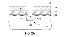
図2Aは、デュアルダマシンプロセス手順を使用してパターン形成された後における配線構造の代表的な断面を示している。配線構造は、基板50上にあり、事前の作成によってメタライゼーション線101を内部に形成された誘電体層100を有している。メタライゼーション線は、一般に、誘電体100内にトレンチをエッチングし次いでそのトレンチに銅などの導電材料を充填することによって作成される。
FIG. 2A shows a representative cross section of a wiring structure after it has been patterned using a dual damascene process procedure. The wiring structure has a
トレンチ内には、銅材料122が誘電体100内に拡散するのを阻止するために使用されるバリア層120がある。バリア層120は、PVD窒化タンタル(TaN)、PVDタンタル(Ta)、ALD TaN、またはこれらの膜の組み合わせで作成することができる。その他のバリア層材料もまた、使用することができる。バリア層102は、上位の誘電体材料104,106を通ってバリア層102へとビアホール114がエッチングされる際に銅材料122が時期尚早に酸化されないように保護するために、平坦化された銅材料122の上に堆積される。バリア層102は、選択性エッチングストップおよび銅拡散バリアとして機能するようにも構成される。代表的なバリア層102材料は、窒化シリコン(SiN)または炭化シリコン(SiC)を含む。
Within the trench is a
バリア層102の上に、ビア誘電体層104が堆積される。ビア誘電体層104は、有機ケイ酸塩ガラス(OSG、炭素ドープ酸化シリコン)または好ましくは低誘電率のその他のタイプの誘電体材料で作成することができる。代表的な二酸化シリコンとしては、PECVD非ドープTEOS二酸化シリコン、PECVDフッ素化シリカガラス(FSG)、HDP FSG、OSG、ポーラスOSGなどを挙げることができる。カリフォルニア州サンタクララのApplied MaterialsによるBlack Diamond (I)およびBlack Diamond (II)、サンノゼのNovellus SystemsによるCoral、アリゾナ州フェニックスのASM America Inc.によるAuroraを含む市販の誘電体材料もまた、使用することができる。ビア誘電体層104の上は、トレンチ誘電体層106である。トレンチ誘電体層106は、炭素ドープ酸化物(C酸化物)などのlow−k誘電体材料であってよい。Low−k誘電体材料の誘電率は、約3.0またはそれ未満であってよい。一実施形態では、ビア誘電体層およびトレンチ誘電体層は、ともに、同じ材料で作成され、同時に堆積されて連続膜を形成する。トレンチ誘電体層106が堆積された後、この(これらの)構造を保持する基板50は、既知の技術によって、ビアホール114およびトレンチ116を形成するためのパターン形成プロセスおよびエッチングプロセスを経る。
A via
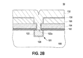
図2Bは、ビアホール114およびトレンチ116の形成後、ビアホール114およびトレンチ116の裏打ちおよび充填のためにバリア層130と銅層132とが堆積されることを示している。バリア層130は、窒化タンタル(TaN)、タンタル(Ta)、ルテニウム(Ru)、またはこれらの膜の異種混合で作成することができる。これらは、一般的に考えられる材料であるが、その他のバリア層材料もまた、使用することができる。次いで、ビアホール114およびトレンチ116を充填するために、銅膜132が堆積される。
FIG. 2B shows that after formation of via
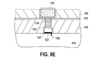
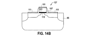
銅膜132によってビアホール114およびトレンチ116を充填した後、基板50は、図2Cに示されるように、誘電体106の表面の上の銅材料(すなわち過剰な銅)およびバリア層(すなわち過剰なバリア)を除去するために化学機械研磨(CMP)によって平坦化される。次のステップは、図2Dに示されるように、コバルト合金などの銅/SiC界面接着促進層135を銅表面140に被せるステップである。コバルト合金の例として、無電解プロセスによって銅の上に選択的に堆積させることができるCoWP、CoWB、またはCoWBPが挙げられる。接着促進層の厚さは、5オングストロームなど僅か数オングストロームの単分子層ほどに薄いものから、Cu拡散バリアとしても機能して誘電体キャップの必要性を排除しえる200〜300オングストロームなど厚めの層であることが可能である。
After filling the via
銅の化学機械研磨(CMP)は、銅腐食防止剤としてベンゾトリアゾール(BTA)を使用することが多い。銅は、BTAとのCu−BTA錯体を形成する。Cu CMPおよびCMP後洗浄を経て処理された基板は、Cu線上および隣接する誘電体上の両方に、図3に白抜きの丸として示されたCu−BTA錯体形態の銅残留物を含有している恐れがある。誘電体上のCu−BTA錯体は、電流漏れまたは金属短絡の増大を阻止するために、除去する必要がある。さらに、図3にべた塗りの丸として示された各種の有機汚染物に加えて、図3において白抜きの三角として示されたTaまたはその他のバリア材料の残留物も少量存在しえる。これらの汚染物に加えて、図3にべた塗りの三角として示されたCuOおよびCuO2に代表される各種の金属酸化物も存在している。Cu−BTA錯体、金属酸化物、および有機汚染物は、基板表面から除去しなければならない3大表面汚染物である。有機物や金属含有化合物の汚染物がない誘電体表面および金属表面を用意することは挑戦であり、湿式プロセスおよび乾式プロセスの両方を含むであろう多段階の表面調整を必要とする。 Copper chemical mechanical polishing (CMP) often uses benzotriazole (BTA) as a copper corrosion inhibitor. Copper forms a Cu-BTA complex with BTA. Substrates processed through Cu CMP and post-CMP cleaning contain copper residues in the form of Cu-BTA complexes, shown as open circles in FIG. 3, both on the Cu lines and on the adjacent dielectric. There is a fear. The Cu-BTA complex on the dielectric needs to be removed to prevent increased current leakage or metal shorting. Furthermore, in addition to the various organic contaminants shown as solid circles in FIG. 3, there may also be a small amount of Ta or other barrier material residue shown as open triangles in FIG. In addition to these contaminants, there are various metal oxides represented by CuO and CuO 2 shown as solid triangles in FIG. Cu-BTA complexes, metal oxides, and organic contaminants are the three major surface contaminants that must be removed from the substrate surface. Providing dielectric and metal surfaces free of organic and metal-containing compound contaminants is a challenge and requires multi-step surface conditioning that would include both wet and dry processes.
以下は、下位の金属の表面調整を行って、上位の金属層を、それら2枚の金属層間の接着に優れた方式で堆積させることを可能にするいくつかの代表的なプロセスフローおよびシステムである。代表的なプロセスフローおよびシステムによって堆積される金属層は、向上されたEM耐性を、したがって全体に低い金属抵抗率を呈すると考えられる。 The following are some representative process flows and systems that allow surface conditioning of the underlying metal to allow the superior metal layer to be deposited in an excellent manner for adhesion between the two metal layers. is there. Metal layers deposited by typical process flows and systems are believed to exhibit improved EM resistance and thus low overall metal resistivity.
1.コバルト合金堆積のための銅表面の設計:
ケースI:金属CMPが誘電体層上で停止する
図4Aは、図2Cに示されたデュアルダマシンビア−トレンチ構造のCMP後銅表面140の上にコバルト合金を無電解堆積させるための表面調整のプロセスフローの一実施形態を示している。図4Aのプロセスフローに使用される基板は、過剰な銅層と、過剰なTaおよび/またはTaNなどのバリア層とを除去するための金属CMP処理を終えたところである。図3に関連した段落において上述されたように、基板表面上には各種の金属汚染物および有機汚染物がある。
1. Design of copper surface for cobalt alloy deposition:
Case I: Metal CMP Stops on Dielectric Layer FIG. 4A illustrates a surface conditioning for electroless deposition of a cobalt alloy on
プロセスは、ステップ401において、Cu−BTA錯体などの金属有機錯体汚染物(すなわち錯化された金属−有機汚染物)と、金属酸化物とを基板表面から除去することによって開始される。金属汚染物は、銅表面および誘電体表面の両方から除去されるが、このステップの目的は、のちに核形成部位として機能する可能性がある潜在金属源を後続のCo合金堆積のために排除することによって、選択性およびCo膜形態の改善を図ることである。銅−BTA錯体、酸化銅(CuOx)、および酸化タンタル(TaOy)などのその他の金属酸化物は、このステップ中に基板表面から除去される。除去される酸化銅の量は、表面上の金属酸化物の汚染物のレベルおよび深さに依存する。金属錯体および金属酸化物は、O2/Arスパッタリングプロセスによって、または1ステップもしくは2ステップの湿式化学的プロセス手順の湿式化学的除去プロセスによって除去することができる。好ましい実施形態は、錯化金属および金属酸化物を除去するために、湿式プロセスを使用する。湿式化学的除去プロセスは、日本の関東化学株式会社によって提供されているDeerCleanなどの有機酸、デラウェア州ウィルミントンのDuPontによって提供されているESC 5800などの半水性溶媒、塩化テトラメチルアンモニウム(TMAH)などの有機塩基、エチレンジアミンやジエチレントリアミンなどの錯化アミン、またはコネティカット州ウェストヘーブンのEnthone, Inc.によって提供されているELD洗浄およびCap Clean 61などの特許化学剤を使用することができる。誘電体表面からのCu−BTAの除去は、Cu−BTAからの銅が、酸化銅に酸化され、引き続きその他の表面調整ステップ中に銅に還元されることによって、選択性を低下させ、Co合金を成長させる予定の誘電体表面上に核形成部位を提供する結果、短絡を引き起こすことおよび漏れ電流を増大させることのないように保証する。したがって、Cu−BTA除去プロセスは、金属短絡または電流漏れに起因する歩留まりの損失を低減させることもできる。
The process begins at
Cu−BTA錯体およびその他の金属酸化物汚染物は、このステップ中に除去されるべき主要な2つの金属汚染物であり、この除去は、制御または非制御のいずれかの雰囲気(すなわち環境)内でなすことができる。例えば、Cu−BTAは、水酸化テトラメチルアンモニウム(TMAH)、またはエチレンジアミンもしくはジエチレントリアミンなどの錯化アミン、またはコネティカット州ウェストヘーブンのEnthone, Inc.によって提供されているELD洗浄およびCap Clean 61などの特許化学剤を含む洗浄溶液をともなう湿式洗浄プロセスによって除去することができる。金属酸化物、なかでも酸化銅は、クエン酸などの弱い有機酸を使用して除去することができる、あるいはその他の有機酸または無機酸を使用することができる。また、硫黄−過酸化物混合などの非常に薄い(すなわち<0.1%の)過酸化物含有酸もまた、使用することができる。湿式洗浄プロセスは、その他の金属残留物または金属酸化物残留物も除去することができる。
Cu-BTA complexes and other metal oxide contaminants are the two major metal contaminants to be removed during this step, and this removal can be in either a controlled or uncontrolled atmosphere (ie, environment). It can be done with. For example, Cu-BTA can be tetramethylammonium hydroxide (TMAH) or complexing amines such as ethylenediamine or diethylenetriamine, or ELD cleaning and
低密度、小隔離、幅広などの異なるパターンまたは特徴タイプの銅線上におけるBTAの存在は、線のパッシベーションの結果であり、その量は、一部には、これらの特徴上に生じるパターン依存性のガルバニック効果の程度に関係する。これは、結果として、パターン依存性のパッシベーション層を形成することがある。この依存性は、さらに、Co合金の堆積特性にも影響することがあり、その結果、ときにインキュベーション効果またはイニシエーション効果とも称されるパターン依存性の堆積特性をもたらす。Cu線からのBTAの除去は、(後続のステップにおいて堆積される予定の)コバルト合金のこのパターン依存性堆積効果を解消し、高密度な隔離特徴内にコバルト合金を均一に堆積可能にするのに有用である。 The presence of BTA on copper wires of different patterns or feature types, such as low density, small isolation, wide, etc., is the result of line passivation, the amount of which is partly due to the pattern-dependence that occurs on these features. Related to the degree of galvanic effect. This may result in the formation of a pattern-dependent passivation layer. This dependence may further affect the deposition characteristics of the Co alloy, resulting in pattern-dependent deposition characteristics, sometimes referred to as incubation effects or initiation effects. Removal of BTA from the Cu line eliminates this pattern-dependent deposition effect of the cobalt alloy (to be deposited in subsequent steps) and allows the cobalt alloy to be deposited uniformly within the dense isolation features. Useful for.
ステップ304において、有機汚染物は、酸素含有プラズマプロセスのように、酸化プラズマによって除去することができる。酸素(O2)プラズマプロセスは、摂氏120度未満の比較的低温で行うことが好ましい。高温O2プラズマプロセスは、銅を分厚い層に酸化し、のちの還元を困難にする傾向がある。したがって、低温のO2プラズマプロセスが好ましい。一実施形態では、O2プラズマプロセスは、下流のプラズマプロセスであってよい。あるいは、有機残留物(すなわち汚染物)は、有機汚染物を物理的に除去するためのO2/Arスパッタリングプロセスを使用して除去することもできる。O2プラズマプロセスおよびO2/Arスパッタリングプロセスは、一般に、1トール未満で動作される。 In step 304, organic contaminants can be removed by an oxidizing plasma, such as an oxygen-containing plasma process. The oxygen (O 2 ) plasma process is preferably performed at a relatively low temperature of less than 120 degrees Celsius. High temperature O 2 plasma processes tend to oxidize copper into thick layers, making subsequent reduction difficult. Therefore, a low temperature O 2 plasma process is preferred. In one embodiment, the O 2 plasma process may be a downstream plasma process. Alternatively, organic residues (ie, contaminants) can be removed using an O 2 / Ar sputtering process to physically remove organic contaminants. O 2 plasma processes and O 2 / Ar sputtering processes are generally operated at less than 1 Torr.
基板表面からCu−BTA、金属酸化物、およびその他の有機汚染物などの汚染物がなくなると、基板は、銅表面を酸化から保護するために、曝露される酸素の量をできる限り少なくすることが望ましい。銅の酸化は、自己制御式のプロセスではない。酸化銅の形成を最小限に抑えるためには、酸素への基板の曝露量および曝露期間を制限する(または制御する)ことが望ましい。酸化銅は、のちのステップで還元されるが、分厚い酸化銅の層は、完全に還元できないことがある。したがって、酸素への銅の曝露は、有機汚染物の除去に必要とされるだけに制限することが重要である。酸素への曝露の制御および制限を達成するためには、基板は、真空下の環境または不活性ガスで満たされた環境などの制御環境内において搬送され処理されることが望ましい。 Once the substrate surface is free of contaminants such as Cu-BTA, metal oxides, and other organic contaminants, the substrate should be exposed to as little oxygen as possible to protect the copper surface from oxidation. Is desirable. Copper oxidation is not a self-regulating process. In order to minimize copper oxide formation, it is desirable to limit (or control) the amount and duration of exposure of the substrate to oxygen. Copper oxide is reduced in a later step, but thick copper oxide layers may not be completely reduced. Therefore, it is important to limit the exposure of copper to oxygen only to that required for the removal of organic contaminants. In order to achieve control and limitation of exposure to oxygen, it is desirable that the substrate be transported and processed in a controlled environment, such as an environment under vacuum or filled with an inert gas.
銅表面に酸化銅がないことを保証するために、基板表面は、ステップ405において、あらゆる残留酸化銅を銅に変換するために還元環境内において再調整される。先の前洗浄ステップは、誘電体層からあらゆる金属を除去しているので、金属の還元は、銅線に対してのみ実施される。銅表面の還元は、水素含有プラズマプロセスによって酸化銅を銅(または実質的に銅)に変換することによって達成することができる。水素含有プラズマを生成するために使用することができる代表的な反応ガスとして、水素(H2)、アンモニア(NH3)、および一酸化炭素(CO)が挙げられる。例えば、基板表面は、水素(H2)ガス、アンモニア(NH3)ガス、または両ガスの組み合わせによって生成される水素含有プラズマによって還元され、基板は、摂氏20度から摂氏300度までの高温にある。一実施形態では、水素プラズマプロセスは、下流のプラズマプロセスである。水素還元プロセスを経ると、基板は、コバルト合金堆積の用意が整う。銅表面は、酸化銅が形成されないことを保証するために、注意深く保護する必要がある。上述のように、コバルト合金の無電解堆積は、酸化銅の存在によって抑制される恐れがある。したがって、処理環境および搬送環境を制御して、酸素への銅表面の曝露を最小限にすることが重要である。
In order to ensure that there is no copper oxide on the copper surface, the substrate surface is reconditioned in a reducing environment in
次のプロセスステップ407では、銅表面の上に、CoWP、CoWB、またはCoWBPなどのコバルト合金が無電解堆積される。コバルト合金の無電解堆積は、湿式プロセスであり、銅表面などの触媒表面上にのみ堆積する。コバルト合金は、銅表面上にのみ選択的に堆積する。
In a
コバルト合金の無電解堆積後、プロセスフローは、随意の堆積後洗浄プロセスステップ409に入ることができる。堆積後洗浄は、ペンシルバニア州アレンタウンのAir Products and Chemical, Inc.によって供給されているCP72Bを含有した溶液などの化学溶液によるブラシスクラブ洗浄を使用して達成することができる。LamのC3(商標)またはP3(商標)洗浄技術などのその他の基板表面洗浄プロセスもまた、使用することができる。その他の後洗浄化学剤は、無電解めっき後に誘電体表面上にとどまるであろうあらゆる金属ベースの汚染物を除去するために、ヒドロキシルアミンをベースにした化学剤を含むことができる。
After electroless deposition of the cobalt alloy, the process flow can enter an optional post-deposition
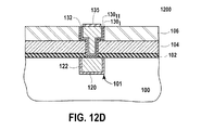
上述のように、プロセス環境およびウエハ搬送環境の制御は、とりわけ銅表面の水素プラズマ還元後などに、コバルト合金堆積のために銅表面を調整するのに非常に重要である。図4Bは、表面処理後の重要なステップにおける酸素への基板表面の曝露を最小限にすることができる代表的な統合システム450の概略図を示している。また、これは統合システムであるので、基板は、1つのプロセスステーションから直ちに次のプロセスステーションへと搬送され、これは、調整後の銅表面が酸素に曝露される時間を制限する。統合システム450は、図4Aのフロー400のプロセス手順全体を通して基板を処理するために使用することができる。
As described above, control of the process environment and wafer transfer environment is very important for conditioning the copper surface for cobalt alloy deposition, particularly after hydrogen plasma reduction of the copper surface. FIG. 4B shows a schematic diagram of an exemplary
上述のように、表面処理、コバルト合金の無電解堆積、および随意のコバルト合金堆積後プロセスは、乾式プロセスと湿式プロセスとの混合をともなう。湿式プロセスは、一般に、近大気で動作され、乾式のO2プラズマ、水素プラズマ、およびO2/Arスパッタリングは、いずれも、1トール未満で動作される。したがって、統合システムは、乾式プロセスと湿式プロセスとの混合を取り扱える必要がある。統合システム450は、3つの基板搬送モジュール(またはチャンバ)460,470,480を有する。搬送チャンバ460,470,480は、基板455を1つのプロセス区域から別のプロセス区域へと移動させるためのロボットを装備している。プロセス区域は、基板カセット、リアクタ、またはロードロックであってよい。基板搬送モジュール460は、実験室雰囲気下で動作される。実験室雰囲気とは、室温下で、大気圧下で、なおかつ粒子欠陥を制御するために一般にUEPAまたはULPAによるフィルタリングを経た空気に曝露された実験室(または工場)環境を指す。モジュール460は、基板455を統合システムに持ち込むためまたは基板をカセット461に戻してシステム450外での処理を続けるために、基板ローダ(または基板カセット)461と連携して機能する。
As mentioned above, surface treatment, electroless deposition of cobalt alloys, and optional post-cobalt alloy deposition processes involve a mix of dry and wet processes. Wet processes are generally operated in the near atmosphere, and dry O 2 plasma, hydrogen plasma, and O 2 / Ar sputtering are all operated at less than 1 Torr. Thus, the integrated system needs to be able to handle a mix of dry and wet processes. The
プロセスフロー400において上述されたように、基板455は、図2Cに示されるように、基板が基板表面から過剰な金属を除去するために金属CMPによって平坦化され、金属トレンチ内にのみ金属を残留させた後、CoWB、CoWP、またはCoWBPなどのコバルト合金を堆積させるために統合システム450に持ち込まれる。プロセスフロー400のステップ401において説明されたように、基板表面は、Cu−BTA錯体などの表面汚染物およびその他の金属酸化物残留物を除去される必要がある。Cu−BTAおよび金属酸化物は、TMAHまたはエチレンジアミンもしくはジエチルアミントリアミンを非限定例として含む錯化アミンを含有した溶液などの洗浄溶液をともなう湿式洗浄プロセスによって除去することができる。BTA金属錯体の除去の次は、銅表面上および誘電体表面上に残留している金属酸化物を、クエン酸または銅に対してある程度選択的に酸化銅を除去できるその他の有機酸を含有した溶液などの洗浄溶液をともなう湿式洗浄プロセスを使用して除去することができる。金属酸化物、なかでも酸化銅は、クエン酸などの弱い有機酸を使用して除去することができる、あるいはその他の有機酸または無機酸を使用することができる。また、硫黄−過酸化物混合などの非常に薄い(すなわち<0.1%の)過酸化物含有酸もまた、使用することができる。湿式洗浄プロセスは、その他の金属残留物または金属酸化物残留物も除去することができる。
As described above in
実験室雰囲気条件で動作する実験室雰囲気搬送モジュール460には、湿式洗浄リアクタ463を統合することができる。湿式洗浄リアクタは、図4Aのステップ401において上述されたように、1ステップまたは2ステップの洗浄を実施するために使用することができる。あるいは、実験室雰囲気搬送モジュール460に追加の湿式洗浄リアクタ463’を統合し、リアクタ463内において2ステップ洗浄プロセスの第1のステップが実施され、リアクタ463’内において第2のステップが実施されるようにすることができる。例えば、リアクタ463内には、Cu−BTAを洗浄するためにTMAHなどの化学剤を含有した洗浄溶液があり、リアクタ463’内には、金属酸化物を洗浄するためにクエン酸などの弱い有機酸を含有した洗浄溶液がある。
A
実験室雰囲気条件は、大気下にあるとともに空気に対して開かれている。湿式洗浄リアクタ463は、プロセスフロー400では実験室雰囲気搬送モジュール460に統合することができるが、このプロセスステップは、金属CMPの直後、基板がコバルト合金堆積のために統合システムに持ち込まれる前に実施することもできる。あるいは、湿式洗浄プロセスは、湿式洗浄ステップの最中および後に制御環境を維持される制御雰囲気プロセス環境内において実施することができる。
Laboratory atmosphere conditions are under air and open to air. The
先の湿式洗浄によって除去されなかった有機残留物(すなわち汚染物)は、Cu−BTAおよび金属酸化物の除去に続く、酸素含有プラズマなどの乾式酸化プラズマプロセス、O2/Arスパッタリング、またはArスパッタリングによって除去することができる。上述のように、プラズマプロセスまたはスパッタリングプロセスの大半は、1トール未満で動作される。したがって、このようなシステム(または装置またはチャンバまたはモジュール)は、圧力が1トール未満などの真空下で動作される搬送モジュールに結合することが望ましい。プラズマプロセスを統合された搬送モジュールが真空下にあれば、搬送モジュールを排気するために長時間を費やす必要がなくなるので、基板の搬送の時間効率は高くなり、プロセスモジュールは真空下に維持される。また、搬送モジュールが真空下にあるゆえに、プラズマプロセスによる洗浄を経た後の基板は、極めて低レベルの酸素に曝露されるだけですむ。有機残留物を洗浄するためにO2プラズマプロセスが選択されると仮定すると、O2プラズマプロセスリアクタ471は、真空搬送モジュール470に結合される。
Organic residues that were not removed by the previous wet clean (ie, contaminants) can be removed by dry oxidation plasma processes such as oxygen-containing plasma, O 2 / Ar sputtering, or Ar sputtering following removal of Cu-BTA and metal oxides. Can be removed. As mentioned above, most plasma or sputtering processes are operated at less than 1 Torr. Accordingly, it is desirable to couple such a system (or apparatus or chamber or module) to a transfer module that is operated under a vacuum, such as a pressure of less than 1 Torr. If the transfer module integrated with the plasma process is under vacuum, there is no need to spend a long time to evacuate the transfer module, so the time efficiency of substrate transfer is high and the process module is kept under vacuum . Also, since the transfer module is under vacuum, the substrate after being cleaned by the plasma process need only be exposed to extremely low levels of oxygen. Assuming an O 2 plasma process is selected to clean the organic residue, the O 2
実験室雰囲気搬送モジュール460は大気で動作され、真空搬送モジュール470は真空下(<1トール)で動作されるので、これらの2つの搬送モジュール間には、異なる圧力下で動作される2つのモジュール460と470との間で基板455を搬送可能にするために、ロードロック465が配される。ロードロック465は、圧力が1トール未満の真空下で動作されるように、実験室雰囲気で動作されるように、または不活性ガスよりなる群から選択される不活性ガスで満たされるように構成される。
Since the laboratory
例えばO2を使用した酸化プラズマ処理を終えた後、基板455は、水素含有還元プラズマ還元チャンバ(またはモジュール)473に移動される。水素含有プラズマによる還元は、一般に、1トール未満の低圧で処理されるので、チャンバは、真空搬送モジュール470に結合される。基板455が水素含有プラズマによって還元されると、銅表面は、酸化銅のないクリーンな状態になる。好ましい一実施形態では、基板455がO2プラズマ処理を終えた後、ウエハをチャンバから取り除くことなくin-situでH2またはH2/NH3プラズマ還元ステップを実施することができる。いずれにせよ、還元プロセスの完了後、基板は、コバルト合金堆積の用意が整う。
For example, after the oxidation plasma treatment using O 2 is finished, the
上述のように、処理環境および搬送環境を制御して、水素含有還元プラズマによる基板の再調整後における酸素への銅表面の曝露を最小限にすることが重要である。基板455は、制御環境下で処理されることが望ましく、その環境は、酸素への基板455の曝露を制限するために、真空下にあるかまたは1種もしくは複数種の不活性ガスで満たされるかのいずれかである。破線490は、図4Bの統合システム450のなかで、環境を制御されている処理システムおよび搬送モジュールの部分の境界を示している。制御環境490下における搬送および処理は、酸素への基板の曝露を制限する。
As mentioned above, it is important to control the processing and transport environment to minimize exposure of the copper surface to oxygen after reconditioning of the substrate with a hydrogen-containing reducing plasma. The
コバルト合金の無電解堆積は、還元剤によって還元された溶液内コバルト種をともなう湿式プロセスである。ここで、還元剤は、リンをベースにしたもの(例えば次亜リン酸塩)、ホウ素をベースにしたもの(例えばジメチルアミンボラン)、またはリンをベースにしたものとホウ素をベースにしたものとの組み合わせであってよい。リンをベースにした還元剤を使用する溶液は、CoWPを堆積させる。ホウ素をベースにした還元剤を使用する溶液は、CoWBを堆積させる。リンをベースにした還元剤とホウ素をベースにした還元剤とを両方使用する溶液は、CoWBPを堆積させる。一実施形態では、コバルト合金無電解堆積溶液は、アルカリ性をベースにしている。あるいは、コバルト合金無電解堆積溶液は、酸性であってもよい。湿式プロセスは、大気圧下で行われるのが一般的であるので、無電解堆積リアクタに結合された搬送モジュール480は、近大気圧で動作されることが望ましい。酸素を含まないように環境が制御されることを保証するために、不活性ガスを使用して制御雰囲気搬送モジュール480を満たすことができる。また、プロセスにおいて使用される全ての流体は、市販の脱ガスシステムによって脱ガスされている、すなわち溶存酸素を除去されている。代表的な不活性ガスとして、窒素(N2)、ヘリウム(He)、ネオン(Ne)、アルゴン(Ar)、クリプトン(Kr)、およびキセノン(Xe)が挙げられる。
Electroless deposition of cobalt alloys is a wet process with in-solution cobalt species reduced by a reducing agent. Here, the reducing agent may be phosphorus based (eg hypophosphite), boron based (eg dimethylamine borane), or phosphorus based and boron based. It may be a combination of A solution using a phosphorus-based reducing agent deposits CoWP. A solution using a boron-based reducing agent deposits CoWB. A solution using both a phosphorus-based reducing agent and a boron-based reducing agent deposits CoWBP. In one embodiment, the cobalt alloy electroless deposition solution is based on alkalinity. Alternatively, the cobalt alloy electroless deposition solution may be acidic. Since wet processes are typically performed under atmospheric pressure, it is desirable that the
一実施形態では、基板が乾燥条件下で無電解堆積システム481に搬入され乾燥条件で同システム481から搬出されること(ドライイン・ドライアウト)を可能にするために、リンスおよび乾燥のシステム(または装置またはモジュール)が湿式コバルト合金無電解堆積リアクタ(または装置またはシステムまたはモジュール)に結合される。ドライイン・ドライアウト要件は、無電解堆積システム481を制御雰囲気搬送モジュール480に統合することを可能にするとともに、別個のリンス乾燥モジュールへとロボット式に湿式搬送するステップの必要性を回避する。無電解堆積システム481の環境は、酸素および水分(水蒸気)のレベルを低くする(または制限する)ように制御される必要もある。また、処理環境内の酸素が低レベルであることを保証するために、不活性ガスを使用してシステムを満たすこともできる。
In one embodiment, a rinsing and drying system (to allow dry-in / dry-out) to be transferred into and out of the
あるいは、コバルト合金無電解堆積は、最近開示された無電解銅堆積と同様に、ドライイン・ドライアウト方式で行うこともできる。銅の無電解堆積のために、ドライイン・ドライアウトの無電解銅プロセスが開発されている。プロセスは、プロキシミティプロセスヘッドを使用して、無電解プロセス液を基板表面上の限られた領域に接触する範囲内に収める。プロキシミティプロセスヘッドの下方にない領域の基板表面は、乾燥している。このようなプロセスおよびシステムの詳細は、2003年6月27日に出願され「Apparatus And Method For Depositing And Planarizing Thin Films On Semiconductor Wafers(半導体ウエハ上に薄膜を堆積させて平坦化するための装置および方法)」と題された米国出願第10/607,611号ならびに2004年6月28日に出願された「Apparatus And Method For Plating Semiconductor Wafers(半導体ウエハにめっきするための装置および方法)」と題された米国出願第10/879,263号に見いだすことができる。これらの両出願は、その全体を本明細書に組み込まれるものとする。コバルト合金の無電解めっきは、ドライイン・ドライアウトのプロセスを可能にするために、同様のプロキシミティプロセスヘッドを使用することができる。 Alternatively, cobalt alloy electroless deposition can be performed in a dry-in / dry-out manner, similar to the recently disclosed electroless copper deposition. A dry-in / dry-out electroless copper process has been developed for the electroless deposition of copper. The process uses a proximity process head to bring the electroless process liquid into contact with a limited area on the substrate surface. The substrate surface in the area not under the proximity process head is dry. Details of such processes and systems have been filed on June 27, 2003, “Apparatus And Method For Depositing And Planarizing Thin Films On Semiconductor Wafers”. No. 10 / 607,611 entitled “Apparatus And Method For Plating Semiconductor Wafers” filed June 28, 2004. US application Ser. No. 10 / 879,263. Both of these applications are incorporated herein in their entirety. Electroless plating of cobalt alloys can use similar proximity process heads to enable dry-in / dry-out processes.
システム481内におけるコバルト合金堆積後、基板455は、随意の堆積後洗浄リアクタに通すことができる。これは、CP72Bもしくはヒドロキシアミンをベースにした洗浄化学剤などの化学剤を使用したブラシスクラブなどの機械的補助を使用して、または浸漬式洗浄、スピンリンス式洗浄、もしくはC3(商標)プロキシミティ技術などのその他の方法を使用して実施することができる。湿式洗浄システム483に対する基板455のドライイン・ドライアウトを可能にするために、ブラシスクラブシステムに、リンスおよび乾燥のシステムを統合する必要もある。システム483内に存在する酸素が制限される(または少ない)ことに保証するために、不活性ガスを使用してシステム483が満たされる。図4Aにおいて上述されたように、堆積後洗浄は随意であるので、システム483は、このシステムが随意であることを示すために破線で示されている。堆積後洗浄ステップは、統合システム450によって動作される最終プロセスであるので、基板455は、処理後にカセット461に戻される必要がある。したがって、洗浄システム483は、あるいは、図4Bに示されるように実験室雰囲気搬送モジュール460に結合することができる。実験室雰囲気搬送モジュール460に結合される場合、洗浄システム483は、制御環境下で動作されず、不活性ガスによって満たされる必要はない。
After cobalt alloy deposition in
上述のように、Cu−BTAおよび金属酸化物を除去するプロセスステップは、金属CMPの直後、基板がコバルト合金堆積のために統合システムに持ち込まれる前に実施することもできる。 As described above, the process step of removing Cu-BTA and metal oxide can also be performed immediately after metal CMP and before the substrate is brought into the integrated system for cobalt alloy deposition.
ケースII:金属CMPがバリア層上で停止する
図5A〜5Cは、処理の諸段階における配線構造の断面を示している。図5Aの基板上の銅層は、CMPによって平坦化されている。バリア層130は、除去されておらず、基板表面上に残っている。図6Aは、デュアルダマシン金属トレンチ内の銅の上にコバルト合金を無電解堆積させるための表面調整のプロセスフローの一実施形態を示している。図6Aのプロセスフロー600で使用される基板は、銅を除去するための銅CMP処理を終えたところである。図5Aに示されるように、基板表面上にはまだバリア層が残っている。ケースIIとケースIとの違いは、ケースIIでは、誘電体106の表面が、Cu−BTA錯体またはその他の銅化合物の残留物に曝露されていないことである。誘電体表面は、ケースIでよりケースIIでのほうが高品質である(すなわち金属汚染物が少ない)。したがって、有機汚染物の除去のためにO2プラズマが使用された後に形成される誘電体層上の酸化銅の除去を目的としたプロセスステップを排除することができる。
Case II: Metal CMP Stops on Barrier Layer FIGS. 5A-5C show cross sections of the wiring structure at various stages of processing. The copper layer on the substrate of FIG. 5A has been planarized by CMP. The
プロセスは、Cu−BTAまたは金属酸化物などの金属汚染物を基板表面から除去するステップ601から開始する。上述のように、Cu−BTA錯体および金属酸化物は、除去されるべき主要な2つの表面金属汚染物である。Cu−BTAおよび金属酸化物などの金属汚染物を基板表面から除去するために使用されるプロセスは、上述されている。例えば、Cu−BTA、および酸化銅を含む金属酸化物は、例えば水酸化テトラメチルアンモニウム(TMAH)またはエチレンジアミンもしくはジエチレントリアミンなどの錯化アミンを含む洗浄溶液をともなう湿式洗浄プロセスによって除去することができる。Cu−BTAの除去は、(のちのステップにおいて堆積される予定の)コバルト合金のパターン依存性堆積効果を解消し、ゆえに、高密度な隔離特徴内にコバルト合金を均一に堆積させることを可能にする。
The process begins at
金属酸化物、より具体的には酸化銅は、クエン酸などの弱い有機酸を使用して除去することができる、あるいはその他の有機酸または無機酸を使用することができる。また、硫黄−過酸化物混合などの非常に薄い(すなわち<0.1%の)過酸化物含有酸もまた、使用することができる。湿式洗浄プロセスは、その他の金属残留物または金属酸化物残留物も除去することができる。 Metal oxides, more specifically copper oxides, can be removed using weak organic acids such as citric acid, or other organic or inorganic acids can be used. Also very thin (ie <0.1%) peroxide-containing acids such as sulfur-peroxide mixtures can be used. The wet cleaning process can also remove other metal residues or metal oxide residues.
Cu表面上およびバリア表面上に残っているBTAを含む有機汚染物は、ステップ602において除去される。有機汚染物は、乾式の酸素(O2)プラズマプロセス、またはH2O、オゾン、もしくは過酸化水素蒸気によるプラズマプロセスなどその他の酸化プラズマプロセスなどのプロセスによって除去することができる。上述のように、酸素含有プラズマプロセスは、摂氏50度未満、好ましくは摂氏120度未満の比較的低温で行われることが好ましい。酸素含有プラズマプロセスは、下流のプラズマプロセスであってよい。あるいは、有機残留物(すなわち汚染物)は、有機汚染物を物理的に除去するためのO2/Arスパッタリングプロセスを使用して除去することもできる。上述のように、O2プラズマプロセスおよびO2/Arスパッタリングプロセスは、一般に、1トール未満で動作される。
Organic contaminants including BTA remaining on the Cu and barrier surfaces are removed in
基板表面からCu−BTA、金属酸化物、および有機汚染物などの汚染物がなくなると、基板は、銅表面をさらなる酸化から保護するために、曝露される酸素の量をできる限り少なくすることが望ましい。表面汚染物が除去された後は、図5Bに示されるように、ステップ603において、Ta、TaN、Ru、またはこれらの材料の組み合わせなどのバリア層が基板表面から除去される。バリア層は、CF4プラズマ、O2/Arスパッタリング、CMPなどのプロセスによって、または湿式化学的エッチングによって除去することができる。CF4プラズマエッチングプロセスおよびO2/Arスパッタリングプロセスは、ともに、1トール未満で動作される。
When the substrate surface is free of contaminants such as Cu-BTA, metal oxides, and organic contaminants, the substrate may be exposed to as little oxygen as possible to protect the copper surface from further oxidation. desirable. After the surface contaminants are removed, as shown in FIG. 5B, in
図5Aの銅表面140に存在している酸化銅およびプラズマ酸化ステップ中に生成された酸化銅は、バリア金属除去ステップ603中に完全に除去されるであろう。したがって、H含有プラズマを使用して銅表面を還元するプロセスは、随意になる。しかしながら、銅表面に酸化銅がないことを保証するために、基板表面は、ステップ605において、あらゆる残留酸化銅を銅に変換するために(随意に)還元することができる。銅表面の還元は、酸化銅を銅に還元するための水素含有プラズマプロセスによって達成することができる。水素含有プラズマプロセスによって使用されるプロセスガスおよびプロセス条件は、ケースIにおいて上述されている。水素還元プロセスを経ると、基板は、コバルト合金堆積の用意が整う。銅表面は、酸化銅が形成されないことを保証するために、酸素から注意深く保護する必要がある。上述のように、コバルト合金の無電解堆積は、酸化銅の存在によって抑制される恐れがある。したがって、処理環境および搬送環境を制御して、酸素への銅表面の曝露を最小限にするまたは排除することが重要である。
The copper oxide present on the
次のプロセスステップ607では、銅表面の上に、CoWP、CoWB、またはCoWBPなどのコバルト合金が無電解堆積される。コバルト合金は、図5Cにおいて、層135として示されている。コバルト合金の無電解堆積は、選択的堆積であり、湿式プロセスである。コバルト合金は、銅表面上にのみ堆積する。
In a
ケースIについて上述されたように、コバルト合金の無電解堆積後、プロセスフローは、随意の堆積後洗浄プロセスステップ609に入ることができる。堆積後洗浄は、無電解堆積プロセスによって誘電体表面上に導入されたあらゆる金属汚染物を除去するために、ペンシルバニア州アレンタウンのAir Products and Chemical, Inc.によって供給されているCP72Bを含有した溶液などの化学溶液によるブラシスクラブ洗浄を使用して、またはヒドロキシアミンをベースにした化学剤によって実施することができる。その他の基板表面洗浄プロセスもまた、使用することができる。
As described above for Case I, after electroless deposition of the cobalt alloy, the process flow can enter an optional post-deposition
上述のように、環境制御は、特に、銅表面のH含有プラズマ還元後などに、コバルト合金堆積のために銅表面を調整するのに非常に重要である。図6Bは、表面処理後の重要なステップにおける酸素への基板表面の曝露を最小限にすることができる代表的な統合システム650の概略図を示している。統合システム650は、図6Aのフロー600のプロセス手順全体を通して基板を処理するために使用することができる。
As mentioned above, environmental control is very important for conditioning the copper surface for cobalt alloy deposition, particularly after H-containing plasma reduction of the copper surface. FIG. 6B shows a schematic diagram of an exemplary
統合システム450と同様に、統合システム650は、3つの基板搬送モジュール660,670,680を有する。搬送モジュール660,670,680は、基板655を1つのプロセス区域から別のプロセス区域へと移動させるためのロボットを装備している。基板搬送モジュール660は、実験室雰囲気下で動作される。モジュール660は、基板655を統合システムに持ち込むためまたは基板をカセット661に戻してシステム650外での処理を続けるために、基板ローダ(または基板カセット)661と連携して機能する。
Similar to the
プロセスフロー600において上述されたように、基板655は、図5Aに示されるように、基板が基板表面から過剰な銅を除去するために銅CMPによって基板が平坦化され、誘電体表面上にバリア層を、そして金属トレンチ内に銅を残留させた後、CoWB、CoWP、またはCoWBPなどのコバルト合金を堆積させるために統合システム650に持ち込まれる。プロセスフロー600のステップ601において説明されたように、基板表面は、Cu−BTA、金属酸化物、および有機残留物などの表面汚染物を除去される必要がある。Cu−BTAおよび金属酸化物は、TMAHを含有した溶液などの洗浄溶液をともなう湿式洗浄プロセスによって除去することができる。湿式洗浄リアクタ663は、実験室雰囲気搬送モジュール660に統合することができる。湿式洗浄リアクタ663は、プロセスフロー600では実験室雰囲気搬送モジュール660に統合することができるが、このプロセスステップは、金属CMPの直後、基板がコバルト合金堆積のために統合システムに持ち込まれる前に実施することもできる。あるいは、湿式洗浄プロセスは、湿式洗浄ステップの最中および後に制御環境を維持される制御雰囲気プロセス環境内において実施することができる。
As described above in the
リアクタ683内において実施された湿式洗浄プロセス601によって除去されなかった有機残留物(すなわち汚染物)は、ステップ602において、O2プラズマなどの乾式プラズマプロセス、またはO2/Arスパッタリングによって除去することができる。上述のように、プラズマプロセスまたはスパッタリングプロセスの大半は、1トール未満で動作される。したがって、このようなシステムは、圧力が1トール未満などの真空下で動作される搬送モジュールに結合することが望ましい。有機残留物を洗浄するためにO2プラズマプロセスが選択されると仮定すると、O2プラズマプロセスリアクタ671は、真空搬送モジュール670に結合される。
Organic residues (ie, contaminants) that have not been removed by the
O2プラズマプロセスは、下流のプラズマプロセスであってよい。O2プラズマリアクタ671は、プロセスフロー600では真空搬送モジュール670に統合することができるが、このプロセスステップは、金属CMPの直後、基板がコバルト合金堆積のために統合システムに持ち込まれる前に実施することもできる。
The O 2 plasma process may be a downstream plasma process. The O 2 plasma reactor 671 can be integrated into the
実験室雰囲気搬送モジュール660は大気下で動作され、真空搬送モジュール670は真空下(<1トール)で動作されるので、これらの2つの搬送モジュール間には、2つのモジュール660と670との間で基板655を搬送可能にするために、ロードロック665が配される。
Since the laboratory
O2プラズマ処理を終えた後、基板655は、ステップ603に示されるように、バリア層エッチングのための処理システムに移動される。乾式のバリアプラズマエッチングプロセスが選択される場合、バリア層エッチングチャンバ(またはモジュール)673は、真空搬送モジュール670に結合することができる。乾式のバリアプラズマプロセスは、CF4プラズマプロセスまたはO2/Arスパッタリングプロセスであってよい。
After finishing the O 2 plasma treatment, the
バリア層のエッチングに続くプロセスは、銅表面上に酸化銅が残らないことを保証するための随意のH含有プラズマ還元である。H2プラズマ還元は、真空搬送モジュール670に結合されたプラズマチャンバ(またはモジュール)674内において実施することができる。あるいは、水素プラズマ還元は、有機残留物を除去するために使用されたO2プラズマリアクタ671内において、残留する酸素種をパージした後に引き続き実施することもできる。
The process following the etching of the barrier layer is an optional H-containing plasma reduction to ensure that no copper oxide remains on the copper surface. H 2 plasma reduction can be performed in a plasma chamber (or module) 674 coupled to a
上述のように、コバルト合金の無電解堆積は、湿式の化学的プロセスである。湿式プロセスは、大気圧で行われるのが一般的であるので、無電解堆積リアクタに結合された搬送モジュール680は、近大気圧で動作されることが望ましい。酸素を含まないように環境が制御されることを保証するために、不活性ガスを使用して制御雰囲気搬送モジュール680を満たすことができる。また、プロセスにおいて使用される全ての流体は、市販の脱ガスシステムによって脱ガスされている、すなわち溶存酸素を除去されている。
As mentioned above, electroless deposition of cobalt alloys is a wet chemical process. Since wet processes are typically performed at atmospheric pressure, it is desirable that the
基板が乾燥条件下で無電解堆積システム681に搬入され乾燥条件で同システム681から搬出されること(ドライイン・ドライアウト)を可能にするためには、湿式コバルト合金無電解堆積リアクタにリンスおよび乾燥のシステムを結合する必要がある。上述のように、ドライイン・ドライアウト要件は、無電解堆積システム681を制御雰囲気搬送モジュール680に統合することを可能にする。システム681は、その中で低い(または制限されたまたは制御された)酸素レベルが維持されることを保証するために、不活性ガスを使用して満たされる。
In order to allow the substrate to be transferred into and out of the
システム681におけるコバルト合金堆積後、基板655は、堆積後洗浄リアクタ683に通すことができる。湿式洗浄システム683に対する基板655のドライイン・ドライアウトを可能にするために、ブラシスクラブシステムに、リンスおよび乾燥のシステムを統合する必要もある。酸素が存在しないことを保証するために、不活性ガスを使用してシステム683が満たされる。図6Aにおいて上述されたように、堆積後洗浄は随意であるので、システム683は、このシステムが随意であることを示すために破線で示されている。堆積後洗浄ステップは、統合システム650によって動作される最終プロセスであるので、基板655は、処理後にカセット661に戻される必要がある。洗浄システム683は、あるいは、実験室雰囲気搬送モジュール660に結合することができる。
After cobalt alloy deposition in
ケースIII:金属CMPが薄い銅層上で停止する
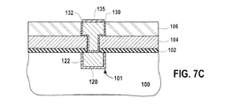
図7A〜7Cは、配線処理の諸段階における配線構造の断面を示している。図7Aの基板は、銅の平坦化を終えたところであり、ただし、基板から完全には銅を取り除かれていない。基板表面上には、薄い銅層132が残っている。図8Aは、デュアルダマシン金属トレンチ内の銅の上にコバルト合金を無電解堆積させるための表面調整のプロセスフローの一実施形態を示している。図8Aのプロセスフロー800で使用される基板は、誘電体層の上のバリア層上方の銅の大半を除去するための銅CMP処理を終えたところである。図7Aに示されるように、バリア表面上には、約100オングストロームから約1000オングストロームまでの範囲内の薄い銅層が残っている。ケースIIIと、ケースIIおよびケースIの両者との違いは、ケースIIIでは、薄い銅層が基板表面全体を覆っており、したがって、銅CMP溶液内に曝される異種物質に起因する銅のガルバニック腐食の懸念がないことである。薄い銅層および存在するその他の表面汚染物は、酸素のない環境内で除去されるので、銅酸化の懸念はない。したがって、H2プラズマ還元は不要である。ケースIIおよびケースIIIは、ともに、バリアCMPがなく、したがって、金属CMP処理の費用が削減される。このプロセスによって調整された銅表面は、誘電体層上対銅上のコバルト合金の選択比を優れたものにすることができる。
Case III: Metal CMP Stops on Thin Copper Layer FIGS. 7A-7C show cross sections of the wiring structure at various stages of wiring processing. The substrate of FIG. 7A has just been planarized with copper, but the copper has not been completely removed from the substrate. A
プロセスは、有機残留物および無機金属酸化物を含む汚染物を基板表面から除去するステップ801から開始する。有機汚染物は、乾式の酸素(O2)プラズマプロセス、H2Oプラズマプロセス、H2O2プラズマプロセス、またはオゾン蒸気をともなうプラズマのように、酸化プラズマによって除去することができる。上述のように、O2プラズマプロセスは、摂氏120度未満の比較的低温で行われることが好ましい。O2プラズマプロセスは、下流のプラズマプロセスであってよい。あるいは、有機残留物(すなわち汚染物)は、有機汚染物を物理的に除去するためのO2/Arスパッタリングプロセスを使用して除去することもできる。上述のように、O2プラズマプロセスおよびO2/Arスパッタリングプロセスは、一般に、1トール未満で動作される。
The process begins at
基板表面から汚染物がなくなると、基板は、銅表面を酸化から保護するために、曝露される酸素の量をできる限り少なくすることが望ましい。表面汚染物が除去された後は、ステップ803において、バリア層および誘電体層の上の薄い銅層が除去される。薄い銅層は、O2/Arスパッタリングによって、O2/ヘキサフルオロアセチルアセトン(HFAC)プラズマエッチングによって、硫酸および過酸化水素などの化学剤を使用した湿式化学的エッチングによって、または錯化化学剤を使用することによって除去することができる。O2/ArスパッタリングプロセスおよびO2/HFACプラズマプロセスは、ともに、1トール未満などの低圧下で動作される。
When the substrate surface is free of contaminants, it is desirable that the substrate be exposed to as little oxygen as possible to protect the copper surface from oxidation. After the surface contaminants are removed, in
その後、ステップ805において、Ta、TaN、または両膜の組み合わせなどのバリア層が基板表面から除去される。薄い銅およびバリアを除去された後の配線構造の断面が、図7Bに示されている。バリア層は、CF4プラズマ、O2/Arスパッタリング、CMP、または湿式化学的エッチングによって、除去することができる。CF4プラズマエッチングプロセスおよびO2/Arスパッタリングプロセスは、ともに、1トール未満で動作される。
Thereafter, in
コバルト合金を選択的に堆積させるための銅表面は、制御雰囲気環境内において、誘電体上方から薄い銅層およびバリア層をエッチングすることによって形成されるので、H含有プラズマを使用して銅表面を還元するプロセスは、ほとんど不要である。しかしながら、銅表面に酸化銅がないことを保証するために、基板表面は、ステップ807において、あらゆる残留酸化銅を銅に変換するために随意に還元することができる。銅表面還元プロセスは、上述されている。水素還元プロセスを経ると、基板は、コバルト合金堆積の用意が整う。銅表面は、酸化銅の形成を阻止するために、注意深く保護する必要がある。次のプロセスステップ809では、銅表面の上に、CoWP、CoWB、またはCoWBPなどのコバルト合金が無電解堆積される。コバルト合金は、図7Cにおいて、層135として示されている。コバルト合金の無電解堆積は、選択的堆積であり、湿式プロセスである。コバルト合金は、銅表面上にのみ堆積する。
The copper surface for selectively depositing the cobalt alloy is formed by etching a thin copper layer and barrier layer from above the dielectric in a controlled atmosphere environment, so that the copper surface is formed using H-containing plasma. The process of reducing is almost unnecessary. However, to ensure that there is no copper oxide on the copper surface, the substrate surface can optionally be reduced in
ケースIおよびケースIIについて上述されたように、コバルト合金の無電解堆積後、プロセスフローは、随意の堆積後洗浄プロセスステップ811に入ることができる。堆積後洗浄は、ケースIおよびケースIIにおいて上述されている。
As described above for Case I and Case II, after electroless deposition of the cobalt alloy, the process flow can enter an optional post-deposition
上述のように、環境制御は、特に銅表面のH含有プラズマ還元後などに、コバルト合金堆積のために銅表面を調整するのに非常に重要である。図8Bは、表面処理後の重要なステップにおける酸素への基板表面の曝露を最小限にすることができる代表的な統合システム850の概略図を示している。統合システム850は、図8Aのフロー800のプロセス手順全体を通して基板を処理するために使用することができる。
As mentioned above, environmental control is very important for conditioning the copper surface for cobalt alloy deposition, particularly after H-containing plasma reduction of the copper surface. FIG. 8B shows a schematic diagram of an exemplary
統合システム850は、3つの基板搬送モジュール860,870,880を有する。搬送モジュール860,870,880は、基板855を1つのプロセス区域から別のプロセス区域へと移動させるためのロボットを装備している。基板搬送モジュール860は、実験室雰囲気下で動作される。モジュール860は、基板855を統合システムに持ち込むためまたは基板をカセット861に戻してシステム850外での処理を続けるために、基板ローダ(または基板カセット)861と連携して機能する。
The
プロセスフロー800において上述されたように、基板855は、図7Aに示されるように、基板表面から過剰な銅を除去するために銅CMPによって基板が平坦化され、誘電体表面の上のバリア層上に薄い銅層を残留させた後、CoWB、CoWP、またはCoWBPなどのコバルト合金を堆積させるために統合システム850に持ち込まれる。プロセスフロー800のステップ801において説明されたように、基板表面は、有機残留物および非銅金属酸化物などの表面汚染物を除去される必要がある。ケースIおよびケースIIとは対照的に、湿式Cu−BTA洗浄を実施する必要性がなくなるので、実験室雰囲気搬送モジュール860を排除して、カセットホルダ861をロードロック865に直接結合させてることも可能であろう。
As described above in
有機残留物および金属酸化物を含む表面汚染物は、O2プラズマなどの酸化プラズマプロセスまたはO2/Arスパッタリングによって除去することができる。上述のように、プラズマプロセスまたはスパッタリングプロセスの大半は、1トール未満で動作される。したがって、このようなシステムは、圧力が1トール未満などの真空下で動作される搬送モジュールに結合することが望ましい。有機残留物を洗浄するためにO2プラズマプロセスが選択されると仮定すると、O2プラズマプロセスリアクタ871は、真空搬送モジュール870に結合される。
Surface contaminants including organic residues and metal oxides can be removed by oxidizing plasma processes such as O 2 plasma or O 2 / Ar sputtering. As mentioned above, most plasma or sputtering processes are operated at less than 1 Torr. It is therefore desirable to couple such a system to a transfer module that is operated under a vacuum, such as a pressure of less than 1 Torr. Assuming an O 2 plasma process is selected to clean the organic residue, the O 2
O2プラズマプロセスは、下流のプラズマプロセスであってよい。O2プラズマリアクタ871は、プロセスフロー800では真空搬送モジュール870に統合することができるが、このプロセスステップは、金属CMPの直後、基板がコバルト合金堆積のために統合システムに持ち込まれる前に実施することもできる。
The O 2 plasma process may be a downstream plasma process. The O 2 plasma reactor 871 can be integrated into the
実験室雰囲気搬送モジュール860は大気下で動作され、真空搬送モジュール870は真空下(<1トール)で動作されるので、これらの2つの搬送モジュール間には、2つのモジュール860と870との間で基板855を搬送可能にするために、ロードロック865が配される。
Since the laboratory
O2プラズマ処理を終えた後、基板855は、ステップ803に示されるように、銅エッチングのための処理システムに移動される。乾式の銅プラズマエッチングプロセスが選択される場合は、銅エッチングチャンバ(またはモジュール)873は、真空搬送モジュール870に結合される。湿式プロセスが選択される場合は、湿式銅エッチングリアクタをリンス/乾燥システムと統合して湿式銅エッチングシステム873’とし、制御雰囲気搬送モジュール880に結合することができる。湿式銅エッチングシステム873’を制御雰囲気搬送モジュール880と統合することを可能にするためには、システム873’に対する基板のドライインおよびドライアウトが必要である。一実施形態では、ドライイン・ドライアウトの要件を満足させるために、湿式銅エッチングシステム873’にリンスおよび乾燥のシステムを組み入れることができる。システム873’の環境は、酸素がないように制御する必要もある。処理環境内に酸素がないことを保証するために、不活性ガスを使用してシステムを満たすこともできる。
After finishing the O 2 plasma treatment, the
ステップ805に示されるように、銅エッチング後にはバリア層エッチングが続く。乾式のバリアプラズマエッチングプロセスが選択される場合は、バリア層エッチングチャンバ874を真空搬送モジュール870に結合することができる。湿式バリアエッチングプロセスが選択される場合は、湿式バリアエッチングリアクタをリンス/乾燥システムと統合して湿式バリアエッチングシステム874’とし、制御雰囲気搬送モジュール880に結合することができる。湿式バリアエッチングシステム874’を制御雰囲気搬送モジュール880と統合することを可能にするためには、システム874’に対する基板のドライインおよびドライアウトが必要である。システム874’の環境は、酸素のレベルを低くする(または制限するまたは制御する)ように制御される必要もある。処理環境内の酸素が低レベルであることを保証するために、不活性ガスを使用してシステムを満たすこともできる。
As shown in
バリア層エッチングに続くプロセスは、上記のような随意のH含有プラズマ還元である。H2プラズマ還元は、真空搬送モジュール870に結合されたプラズマチャンバ877内において実施することができる。
The process following the barrier layer etch is an optional H-containing plasma reduction as described above. H 2 plasma reduction can be performed in a
上述のように、コバルト合金の無電解堆積は、湿式プロセスである。湿式プロセスは、大気圧下で行われるのが一般的であるので、無電解堆積リアクタに結合された搬送モジュール680は、近大気圧で動作されることが望ましい。酸素レベルが低くなるように環境が制御されることを保証するためには、不活性ガスを使用して制御雰囲気搬送モジュール880を満たすことができる。また、プロセスにおいて使用される全ての流体は、市販の脱ガスシステムによって脱ガスされている、すなわち溶存酸素を除去されている。代表的な不活性ガスとして、窒素(N2)、ヘリウム(He)、ネオン(Ne)、アルゴン(Ar)、クリプトン(Kr)、およびキセノン(Xe)が挙げられる。
As mentioned above, the electroless deposition of cobalt alloy is a wet process. Since wet processes are typically performed under atmospheric pressure, it is desirable that the
基板が乾燥条件下で無電解堆積システム881に搬入され乾燥条件で同システム881から搬出されること(ドライイン・ドライアウト)を可能にするためには、湿式コバルト合金無電解堆積リアクタにリンスおよび乾燥のシステムを結合する必要がある。ドライイン・ドライアウト要件は、無電解堆積システム881を制御雰囲気搬送モジュール880に統合することを可能にする。システム881は、その中に存在する酸素が低レベルであることを保証するために、不活性ガスを使用して満たされる。
In order to allow the substrate to be transferred into and out of the
システム881におけるコバルト合金堆積後、基板855は、堆積後洗浄リアクタに通すことができる。湿式洗浄システム883に対する基板855のドライイン・ドライアウトを可能にするためには、ブラシスクラブシステムにリンスおよび乾燥のシステムを統合する必要もある。酸素が存在しないことを保証するために、不活性ガスを使用してシステム883が満たされる。図8Aにおいて上述されたように、堆積後洗浄は随意であるので、システム883は、このシステムが随意であることを示すために破線で示されている。堆積後洗浄ステップは、統合システム850によって動作される最終プロセスであるので、基板855は、処理後にカセット861に戻される必要がある。洗浄システム883は、あるいは、実験室雰囲気搬送モジュール860に結合することができる。
After cobalt alloy deposition in
2.無電解銅堆積のためのバリア表面の設計:
上述のシステム概念は、銅めっきのためにバリア表面を調整するために使用することができる。Ta、TaN、またはRuなどのバリア層は、長期間にわたって空気に曝露されると、TaxOy(酸化タンタル)、TaOxNy(窒酸化タンタル)、またはRuO2(酸化ルテニウム)を形成する恐れがある。基板上への金属層の無電解堆積は、基板の表面特性および組成に大きく依存する。Ta、TaN、またはRuの表面上への銅の無電解めっきは、電解めっきに先立つシード層の形成およびリソグラフィ的に画定されたパターン内へのCu線の選択的堆積の双方にとっての関心事である。懸念の1つは、酸素(O2)の存在下において形成される原子的に薄い自然金属酸化物の層によって、無電解堆積プロセスが抑制されることである。
2. Barrier surface design for electroless copper deposition:
The system concept described above can be used to condition the barrier surface for copper plating. Barrier layers such as Ta, TaN, or Ru form Ta x O y (tantalum oxide), TaO x N y (tantalum oxynitride), or RuO 2 (ruthenium oxide) when exposed to air for extended periods of time. There is a fear. Electroless deposition of a metal layer on a substrate is highly dependent on the surface properties and composition of the substrate. Electroless plating of copper on Ta, TaN, or Ru surfaces is a concern for both the formation of a seed layer prior to electroplating and the selective deposition of Cu lines in a lithographically defined pattern. is there. One concern is that the electroless deposition process is suppressed by an atomically thin layer of native metal oxide formed in the presence of oxygen (O 2 ).
また、銅膜は、酸化タンタルや、窒酸化タンタル、酸化ルテニウムなどのバリア酸化物層には接着せず、Ta膜や、Ru膜、TaリッチTaN膜などの純粋なバリア金属膜またはバリア層リッチ膜には接着する。Taおよび/またはTaNのバリア層は、例として使用されるに過ぎない。説明および概念は、Ruの薄い層を被せられたTaまたはTaNのようなその他のタイプのバリア金属にも当てはまる。上述のように、乏しい接着は、EM耐性に悪影響を及ぼす恐れがある。また、バリア層表面上への酸化タンタルまたは窒酸化タンタルの形成は、バリア層の抵抗率を増大させる恐れがある。これらの問題ゆえに、統合システムを使用してバリア/銅界面を調整し、バリア層と銅との間に優れた接着を保証することおよびバリア層の抵抗率を小さく保証することが望まれる。 In addition, the copper film does not adhere to a barrier oxide layer such as tantalum oxide, tantalum nitride oxide, or ruthenium oxide, but is pure barrier metal film or barrier layer rich such as Ta film, Ru film, or Ta-rich TaN film. Adhere to the membrane. Ta and / or TaN barrier layers are only used as examples. The description and concept apply to other types of barrier metals such as Ta or TaN coated with a thin layer of Ru. As mentioned above, poor adhesion can adversely affect EM resistance. In addition, the formation of tantalum oxide or tantalum oxynitride on the barrier layer surface may increase the resistivity of the barrier layer. Because of these problems, it is desirable to use an integrated system to tune the barrier / copper interface to ensure good adhesion between the barrier layer and copper and to ensure a low barrier layer resistivity.
ケースI:金属線の形成
図9Aは、誘電体エッチングによってパターン形成されフォトレジストを除去された後における金属線構造の代表的な断面を示している。金属線構造は、基板900上にあり、事前の作成によってゲート酸化物121、スペーサ107、およびコンタクト125をともなうゲート構造105を内部に形成されたシリコン層110を有している。コンタクト125は、一般に、酸化物103内にコンタクトホールをエッチングし次いでそのコンタクトホールにタングステンなどの導電性材料を充填することによって作成される。代替の材料として、銅、アルミニウム、またはその他の導電性材料が挙げられる。バリア層102は、選択的なトレンチエッチングストップとして機能するようにも構成される。バリア層102は、窒化シリコン(SiN)または炭化シリコン(SiC)などの材料で作成することができる。
Case I: Metal Line Formation FIG. 9A shows a typical cross section of a metal line structure after patterning by dielectric etching and removal of the photoresist. The metal line structure is on a
バリア層102の上に、金属線誘電体層106が堆積される。106の堆積に使用することができる誘電体材料は、上述されている。誘電体層106の堆積後、基板は、金属トレンチ106を形成するために、パターン形成されエッチングされる。図9Bは、金属トレンチ116の形成後、金属トレンチ116に裏打ちするために金属バリア層130が堆積されることを示している。図9Cは、バリア層130が堆積された後、バリア層130の上に銅層132が堆積されることを示している。バリア層130は、窒化タンタル(TaN)、タンタル(Ta)、Ru、またはこれらの膜の組み合わせで作成することができる。次いで、金属トレンチ116に充填するために、銅膜132が堆積される。一実施形態では、銅膜132は、その下に薄い銅シード層131を含む。
A metal
プラズマ表面前処理を使用して共形の薄い銅シード層131の堆積のための触媒表面を調整し、銅膜132でトレンチ116を充填した後、基板900は、図9Dに示されるように、誘電体106の表面の上の銅材料(すなわち過剰な銅)およびバリア層(すなわち過剰なバリア)を除去するために、化学的になおかつ機械的に研磨(CMP)される、または湿式エッチングされる。一実施形態では、薄い銅シード層の厚さは、約5オングストロームから約300オングストロームまでの間である。次のステップは、図9Eに示されるように、コバルト合金などの銅/SiC界面接着促進層135を銅表面140に被せるステップである。コバルト合金の例として、無電解プロセスによって銅の上に選択的に堆積させることができるCoWP、CoWB、またはCoWBPが挙げられる。接着促進層の厚さは、5オングストロームなど僅か数オングストロームの単分子層ほどに薄いものから、200オングストロームなど厚めの層であることが可能である。
After conditioning the catalyst surface for deposition of the conformal thin
図10Aは、トレンチが形成された後に、無電解銅堆積のためにバリア(またはライナ)層表面を調整するプロセスフロー1000の一実施形態を示している。しかしながら、バリア(またはライナ)層は、ALD堆積リアクタまたはPLD堆積リアクタなどの非統合型堆積システム内において個別に調整されてもよい。この場合、薄い銅シード層を堆積させるための表面調整は、金属プラグ前洗浄およびバリア堆積のプロセスステップを含まないと考えられる。ステップ1001では、自然金属酸化物を除去するためにコンタクトプラグの上面124aが洗浄される。金属酸化物は、Arスパッタリングプロセス、またはNF3、CF4、もしくは両者の組み合わせなどのフッ素含有ガスを使用したプラズマプロセス、または湿式化学的エッチングプロセス、または例えば水素含有プラズマを使用した還元プロセスによって除去することができる。ステップ1003では、バリア層が堆積される。金属線およびビア限界寸法の縮小ゆえに、バリア層は、技術ノード次第では、原子層成長(ALD)によって堆積させることができる。バリア層130の厚さは、約20オングストロームから約200オングストロームまでの間である。上述のように、バリア層の酸素への曝露を防ぐことは、銅がバリア層との間の接着に優れた方式でバリア層上に無電解堆積されることを保証するのに重要である。バリア層が堆積されると、基板は、酸素への曝露を制限するために、制御雰囲気環境内において搬送または処理されることが望ましい。バリア層は、後続の銅シード堆積ステップのための触媒表面を提供するために、随意のステップ1005において、Ta、TaN、またはRuの層上に金属リッチ表面を形成するための水素プラズマ処理を施される。このステップが必要であるか否かは、表面がどの程度金属リッチであるかに依存する。
FIG. 10A illustrates one embodiment of a
その後、ステップ1007において、バリア表面上に共形の銅シードが堆積され、そして、ステップ1008において、厚い銅のギャップ充填(またはバルク充填)プロセスが続く。一実施形態では、共形の銅シード層は、無電解プロセスによって堆積させることができる。厚い銅のバルク充填プロセスは、無電解堆積(ELD)プロセスまたは電解めっき(ECP)プロセスであってよい。無電解銅堆積およびECPは、周知の湿式プロセスである。上述のような制御された処理および搬送の環境をともなうシステムに湿式プロセスを統合させるには、リアクタをリンス/ドライヤに統合し、ドライイン・ドライアウトのプロセス能力を可能にする必要がある。また、システムは、酸素への基板の曝露が最小限であることを保証するために、不活性ガスで満たされる必要がある。近年では、ドライイン・ドライアウトの無電解銅プロセスが開発されている。さらに、プロセスにおいて使用される全ての流体は、市販の脱ガスシステムによって脱ガスされている、すなわち溶存酸素を除去されている。
Thereafter, in
無電解堆積プロセスは、パドルめっきなどの数々の方式で行うことができる。パドルめっきでは、流体が基板上に供給され、静止した状態で反応を進められる。その後、反応剤は、除去され廃棄される、または再生される。別の一実施形態では、プロセスは、プロキシミティプロセスヘッドを使用して、無電解プロセス液を基板表面上の限られた領域に接触する範囲内に収める。プロキシミティプロセスヘッドの下方にない領域の基板表面は、乾燥している。このようなプロセスおよびシステムの詳細は、2003年6月27日に出願され「Apparatus And Method For Depositing And Planarizing Thin Films On Semiconductor Wafers(半導体ウエハの薄膜を堆積させ平坦化するための装置および方法)」と題された米国出願第10/607,611号および2004年6月28日に出願された「Apparatus And Method For Plating Semiconductor Wafers(半導体ウエハにめっきするための装置および方法)」と題された米国出願第10/879,263号に見いだすことができる。これらの両出願は、その全体を本明細書に組み込まれるものとする。前述のコバルト合金の無電解めっきは、同様のプロキシミティプロセスヘッドを使用してドライイン・ドライアウトのプロセスを可能にすることができる。
The electroless deposition process can be performed in a number of ways, such as paddle plating. In paddle plating, a fluid is supplied onto a substrate and the reaction is allowed to proceed in a stationary state. The reactant is then removed and discarded or regenerated. In another embodiment, the process uses a proximity process head to bring the electroless process liquid into contact with a limited area on the substrate surface. The substrate surface in the area not under the proximity process head is dry. Details of such processes and systems were filed on June 27, 2003, “Apparatus And Method For Depositing And Planarizing Thin Films On Semiconductor Wafers”. United States Application No. 10 / 607,611 entitled "Apparatus And Method For Plating Semiconductor Wafers" filed June 28, 2004
ステップ1007,1008における銅堆積後、基板は、ステップ1009において、随意の基板洗浄を経ることができる。銅堆積後の洗浄は、ペンシルバニア州アレンタウンのAir Products and Chemical, Inc.によって供給されているCP72Bを含有した溶液などの化学溶液によるブラシスクラブ洗浄を使用して達成することができる。LamのC3(商標)またはP3(商標)による洗浄技術などのその他の基板表面洗浄プロセスもまた、使用することができる。
After copper deposition in
図10Bは、バリア表面調整後における基板表面の酸素への曝露を最小限にすることができる統合システム1050の概略図の一実施形態を示している。また、これは統合システムであるので、基板は、1つのプロセスステーションから直ちに次のプロセスステーションへと搬送され、これは、クリーンな銅表面が低レベルの酸素に曝露される時間を制限する。統合システム1050は、図10Aのフロー1000のプロセス手順全体を通して基板を処理するために使用することができる。
FIG. 10B illustrates one embodiment of a schematic diagram of an
上述のように、銅の無電解堆積のための表面調整、および随意のコバルト合金堆積後プロセスは、乾式プロセスと湿式プロセスとの混合をともなう。湿式プロセスは、一般に、近大気で動作され、乾式プラズマプロセスは、1トール未満で動作される。したがって、統合システムは、乾式プロセスと湿式プロセスとの混合を取り扱える必要がある。統合システム1050は、3つの基板搬送モジュール1060,1070,1080を有する。搬送モジュール1060,1070,1080は、基板1055を1つのプロセス区域から別のプロセス区域へと移動させるためのロボットを装備している。プロセス区域は、基板カセット、リアクタ、またはロードロックであってよい。基板搬送モジュール1060は、実験室雰囲気下で動作される。モジュール1060は、基板1555を統合システムに持ち込むためまたは基板をカセット1061の1つに戻すために、基板ローダ(または基板カセット)1061と連携して機能する。
As mentioned above, surface conditioning for the electroless deposition of copper, and the optional post-cobalt alloy deposition process, involves a mix of dry and wet processes. Wet processes are generally operated in the near atmosphere and dry plasma processes are operated at less than 1 Torr. Thus, the integrated system needs to be able to handle a mix of dry and wet processes. The
プロセスフロー1000において上述されたように、基板1055は、バリア層および銅層を堆積させるために、統合システム1050に持ち込まれる。プロセスフロー1000のステップ1001において説明されたように、自然酸化タングステンを除去するために、コンタクト125のタングステン上面124aがエッチングされる。酸化タングステンが除去されると、露出された図9Aのタングステン表面124aは、酸素に曝露されないように保護される必要がある。もし、除去プロセスがArスパッタリングプロセスであるならば、リアクタ1071は、真空搬送モジュール1070に結合される。もし、湿式の化学的エッチングプロセスが選択されるならば、リアクタは、タングステン表面の酸素への曝露を制限するために、実験室雰囲気搬送モジュール1060ではなく、制御雰囲気搬送モジュール1080に結合されることが望ましい。
As described above in
その後、基板は、図10Aのステップ1003において説明されたように、Ta、TaN、Ru、またはこれらの膜の組み合わせなどの金属バリア層を堆積される。図9Bのバリア層130は、ALDプロセスまたはPVDプロセスによって堆積させることができる。一実施形態において、ALDプロセスは、1トール未満で動作される。ALDリアクタ1073は、真空搬送モジュール1070に結合される。別の一実施形態では、堆積プロセスは、金属バリアを形成するために超臨界CO2および有機金属前駆体を使用する高圧プロセスである。さらに別の一実施形態では、堆積プロセスは、1トール未満の圧力で動作する物理気相成長(PVD)プロセスである。超臨界CO2を使用した高圧プロセスのための代表的リアクタの詳細が、2003年2月3日に出願され「Method and Apparatus For Semiconductor Wafer Cleaning Using High-Frequency Acoustic Energy with Supercritical Fluid(超臨界流体とともに高周波音響エネルギを使用した半導体ウエハ洗浄のための方法および装置)」と題された同一出願人による出願第10/357,664号に記載されている。この出願は、参照のために本明細書に組み込まれるものとする。
The substrate is then deposited with a metal barrier layer, such as Ta, TaN, Ru, or a combination of these films, as described in
基板は、図10Aのステップ1005において説明されたように、例えば水素含有プラズマを使用した随意の還元プロセスを経ることができる。水素還元リアクタ1074は、真空搬送モジュール1070に結合することができる。この段階で、基板は、無電解銅堆積の用意が整う。無電解銅めっきは、無電解銅めっきリアクタ1081内において共形のシード層を堆積させて実施することができる。シード層の堆積に続いて、共形シード層の堆積に使用されたのと同じ無電解銅堆積リアクタ1081内において、ただし、バルク充填を達成するための異なる化学物質を使用して、銅のバルク充填を実施することができる。あるいは、銅のバルク充填は、別個のECPリアクタ1081’内において実施することができる。
The substrate can undergo an optional reduction process using, for example, a hydrogen-containing plasma, as described in
統合システム1050を後にする前に、基板は、先の銅堆積プロセスからの残留物を洗浄することができる表面洗浄プロセスを随意に経ることができる。例えば、基板洗浄プロセスは、ブラシ洗浄プロセスであってよい。基板洗浄リアクタ1083は、制御雰囲気搬送モジュール1080に統合することができる。あるいは、基板洗浄リアクタ1083は、実験室雰囲気搬送モジュール1060に統合することもできる。
Prior to leaving the
あるいは、図9Bのバリア層130は、基板900が表面処理および銅堆積のためにシステムに持ち込まれる前に、プロセスチャンバ内において堆積させることができる。図10Cは、無電解銅堆積のためにバリア(またはライナ)層表面を調整するプロセスフロー1090の一実施形態を示している。バリア表面は、後続の銅シード堆積ステップのための触媒表面を提供するために、随意のステップ1095において、Ta、TaN、またはRuの層上に金属リッチ表面を形成するために水素プラズマ処理を施される。このステップが必要であるか否かは、表面がどの程度金属リッチであるかに依存する。
Alternatively, the
その後、ステップ1097において、バリア表面上に共形の銅シードが堆積され、そして、ステップ1098において、厚い銅のギャップ充填(またはバルク充填)プロセスが続く。一実施形態では、共形の銅シード層は、無電解プロセスによって堆積させることができる。厚い銅のバルク充填プロセスは、無電解堆積(ELD)プロセスまたは電解めっき(ECP)プロセスであってよい。ステップ1097,1098における銅堆積後、基板は、ステップ1099において、随意の基板洗浄を経ることができる。銅堆積後の洗浄は、ペンシルバニア州アレンタウンのAir Products and Chemical, Inc.によって供給されているCP72Bを含有した溶液などの化学溶液によるブラシスクラブ洗浄を使用して達成することができる。LamのC3(商標)またはP3(商標)による洗浄技術などのその他の基板表面洗浄プロセスもまた、使用することができる。
Thereafter, in
図10Dは、バリア表面調整後の重要なステップにおける酸素への基板表面の曝露を最小限にすることができる統合システム1092の概略図の一実施形態を示している。また、これは統合システムであるので、基板は、1つのプロセスステーションから直ちに次のプロセスステーションへと搬送され、これは、クリーンな銅表面が低レベルの酸素に曝露される時間を制限する。統合システム1092は、図10Cのフロー1090のプロセス手順全体を通して基板を処理するために使用することができる。
FIG. 10D shows one embodiment of a schematic diagram of an
上述のように、銅の無電解堆積のための表面調整、および随意のコバルト合金堆積後プロセスは、乾式プロセスと湿式プロセスとの混合をともなう。湿式プロセスは、一般に、近大気で動作され、乾式プラズマプロセスは、1トール未満で動作される。したがって、統合システムは、乾式プロセスと湿式プロセスとの混合を取り扱える必要がある。統合システム1092は、3つの基板搬送モジュール1060,1070,1080を有する。搬送モジュール1060,1070,1080は、基板1055を1つのプロセス区域から別のプロセス区域へと移動させるためのロボットを装備している。プロセス区域は、基板カセット、リアクタ、またはロードロックであってよい。基板搬送モジュール1060は、実験室雰囲気下で動作される。モジュール1060は、基板1555を統合システムに持ち込むためまたは基板をカセット1061の1つに戻すために、基板ローダ(または基板カセット)1061と連携して機能する。
As mentioned above, surface conditioning for the electroless deposition of copper, and the optional post-cobalt alloy deposition process, involves a mix of dry and wet processes. Wet processes are generally operated in the near atmosphere and dry plasma processes are operated at less than 1 Torr. Thus, the integrated system needs to be able to handle a mix of dry and wet processes. The
プロセスフロー1090において上述されたように、基板1055は、バリア層の堆積後、無電解銅堆積のためにバリア表面を調整するために統合システム1092に持ち込まれる。基板は、図10Cのステップ1095において説明されたように、例えば水素含有プラズマを使用した還元プロセスを先ず経る。水素還元リアクタ1074は、真空搬送モジュール1070に結合することができる。この段階で、基板は、無電解銅堆積の用意が整う。無電解銅めっきは、無電解銅めっきリアクタ1081内において共形のシード層を堆積させて実施することができる。シード層の堆積に続いて、共形シード層の堆積に使用されたのと同じ無電解銅堆積リアクタ1081内において、ただし、バルク充填を達成するための異なる化学物質を使用して、銅のバルク充填を実施することができる。あるいは、銅のバルク充填は、別個のECPリアクタ1081’内において実施することができる。
As described above in
統合システム1092を後にする前に、基板は、先の銅堆積プロセスからの残留物を洗浄することができる表面洗浄プロセスを随意に経ることができる。例えば、基板洗浄プロセスは、ブラシ洗浄プロセスであってよい。基板洗浄リアクタ1083は、制御雰囲気搬送モジュール1080に統合することができる。あるいは、基板洗浄リアクタ1083は、実験室雰囲気搬送モジュール1060に統合することもできる。
Prior to leaving the
図11Aは、無電解銅堆積のためにバリア(またはライナ)層表面を調整するとともに無電解コバルト合金堆積のためにCMP後の銅表面を調整するプロセスフローの一実施形態を示している。ステップ1101では、自然酸化タングステンを除去するためにコンタクトプラグの上面124aが洗浄される。金属酸化物は、Arスパッタリングプロセス、プラズマ還元プロセス、反応性イオンエッチングプロセス、または湿式化学的エッチングプロセスによって除去することができる。ステップ1103では、バリア層が堆積される。バリア層は、後続の銅シード堆積ステップのための触媒表面を提供するために、随意のステップ1005において、Ta、TaN、またはRuの層上に金属リッチ表面を形成するために水素プラズマ処理を施される。このステップが必要であるか否かは、表面がどの程度金属リッチであるかに依存する。
FIG. 11A illustrates one embodiment of a process flow for adjusting the barrier (or liner) layer surface for electroless copper deposition and adjusting the post-CMP copper surface for electroless cobalt alloy deposition. In
しかしながら、バリア(またはライナ)層は、ALD堆積リアクタまたはPLD堆積リアクタなどの非統合型堆積システム内において個別に調整されてもよい。この場合、薄い銅シード層を堆積させるための表面調整は、図10Aのステップ1001,1003および図11Aのステップ1101,1103において説明されたような金属プラグ前洗浄およびバリア堆積のプロセスステップを含まないと考えられる。これらのケースでは、説明されたプロセスは、ステップ1005または1105から始まる。
However, the barrier (or liner) layer may be tailored in a non-integrated deposition system such as an ALD deposition reactor or a PLD deposition reactor. In this case, surface conditioning to deposit a thin copper seed layer does not include the metal plug pre-clean and barrier deposition process steps as described in
その後、ステップ1107において、バリア表面上に共形の銅シードが堆積され、そして、ステップ1108において、厚い銅のギャップ充填(またはバルク充填)プロセスが続く。一実施形態では、共形の銅シード層は、無電解プロセスによって堆積させることができる。厚い銅のバルク充填プロセスは、無電解堆積プロセス(ELD)または電解めっき(ECP)プロセスであってよい。無電解銅堆積およびECPは、周知の湿式プロセスである。上述のような制御された処理および搬送の環境をともなうシステムに湿式プロセスを統合させるには、リアクタをリンス/ドライヤに統合し、ドライイン・ドライアウトのプロセス能力を可能にする必要がある。また、システムは、酸素への基板の曝露が最小限であることを保証するために、不活性ガスで満たされる必要がある。近年では、ドライイン・ドライアウトの無電解銅プロセスが開発されている。さらに、プロセスにおいて使用される全ての流体は、市販の脱ガスシステムによって脱ガスされている、すなわち溶存酸素を除去されている。
Thereafter, in
ステップ1107において、基板に共形の銅シードが堆積され、ステップ1108において、無電解プロセスまたは電解めっきプロセスのいずれかによって厚いCuのギャップ充填(バルク充填)がなされた後、図9Dに示されるように、ステップ1109において、誘電体106の上のバリア層130上方の基板表面から銅層132が除去される。バリア層は、その後、除去される。これらの除去プロセスは、ともに、図11Aのプロセスステップ1109において実施される。バリア層上方の表面からの銅の除去は、湿式プロセスであるCMPによって達成することができる。バリア層は、CF4プラズマなどの反応性イオンエッチング、O2/Arスパッタリング、CMP、または湿式化学的エッチングによって除去することができる。これらのバリアエッチングプロセスについては、前述されている。
In
バリア層の除去後は、基板表面から汚染物を除去するために、Cu−BTA錯体および金属酸化物を除去するための洗浄プロセス(ステップ1110)と、有機汚染物を除去するプロセス(ステップ1111)とが実施される。金属CMP後にこれらの2つのステップを使用して基板表面を洗浄する詳細については、上述されている。 After removing the barrier layer, in order to remove contaminants from the substrate surface, a cleaning process for removing Cu-BTA complex and metal oxide (step 1110) and a process for removing organic contaminants (step 1111). And are carried out. Details of cleaning the substrate surface using these two steps after metal CMP are described above.
基板表面から表面汚染物が除去された後、基板は、ステップ1112において、残留する全ての金属酸化物を金属に還元するために還元プラズマ(水素含有プラズマ)による処理を施される。水素還元後、銅表面は、非常にクリーンでなおかつ触媒性であり、コバルト合金の無電解堆積の用意が整う。ステップ1113において、基板は、コバルト合金の無電解堆積と、基板のリンスおよび乾燥とを経る。最終プロセスステップ1115は、先の無電解コバルト合金堆積からのあらゆる残留汚染物を洗浄するための随意の基板洗浄ステップである。
After surface contaminants are removed from the substrate surface, the substrate is treated in
図11Bは、バリア表面および銅表面の調整後の重要なステップにおける酸素への基板表面の曝露を最小限にすることができる統合システム1150の概略図の一実施形態を示している。また、これは統合システムであるので、基板は、1つのプロセスステーションから直ちに次のプロセスステーションへと搬送され、これは、クリーンな銅表面が低レベルの酸素に曝露される時間を制限する。統合システム1150は、図11Aのフロー1100のプロセス手順全体を通して基板を処理するために使用することができる。
FIG. 11B shows one embodiment of a schematic diagram of an
統合システム1150は、3つの基板搬送モジュール1160,1170,1180を有する。搬送モジュール1160,1170,1180は、基板1155を1つのプロセス区域から別のプロセス区域へと移動させるためのロボットを装備している。プロセス区域は、基板カセット、リアクタ、またはロードロックであってよい。基板搬送モジュール1160は、実験室雰囲気下で動作される。モジュール1160は、基板1155を統合システムに持ち込むためまたは基板をカセット1161の1つに戻すために、基板ローダ(または基板カセット)1161と連携して機能する。
The
図11Aのプロセスフロー1100において上述されたように、基板1155は、バリア層を堆積させるため、銅層堆積のためにバリア表面を調整するため、そして無電解コバルト合金堆積のためにCMP後の銅表面を調整するために、統合システム1150に持ち込まれる。プロセスフロー1100のステップ1101において説明されたように、自然金属酸化物を除去するために、コンタクト125の金属プラグ上面124aがエッチングされる。あるいは、金属プラグ表面の酸化物は、水素含有プラズマなどの還元プラズマを使用して除去することができる。金属プラグ表面の酸化物が除去されると、露出された図9Aの金属表面124aは、酸素に曝露されないように保護される必要がある。もし、除去プロセスがArスパッタリングプロセスであるならば、Arスパッタリングリアクタ1171は、真空搬送モジュール1170に結合される。もし、湿式の化学的エッチングプロセスが選択されるならば、リアクタは、クリーンな金属プラグ表面の酸素への曝露を制限するために、実験室雰囲気搬送モジュール1160ではなく、制御雰囲気搬送モジュール1180に結合されることが望ましい。
As described above in the
その後、基板は、図11Aのステップ1103において説明されたように、Ta、Ru、TaN、またはこれらの膜の組み合わせなどの金属バリア層を堆積される。図9Bのバリア層130は、ALDプロセスまたはPVDプロセスによって堆積させることができる。一実施形態では、ALDプロセスは、1トール未満で動作される。ALDリアクタ1173は、真空搬送モジュール1170に結合される。別の一実施形態では、堆積プロセスは、金属バリアを形成するために超臨界CO2および有機金属前駆体を使用する高圧プロセスである。さらに別の一実施形態では、堆積プロセスは、1トール未満の圧力で動作される物理気相成長(PVD)プロセスである。基板は、図11Aのステップ1105において説明されたように、例えば水素含有プラズマを使用した随意の還元プロセスを経ることができる。水素還元リアクタ1174は、真空搬送モジュール1170に結合することができる。この段階で、基板は、無電解銅堆積の用意が整う。無電解銅めっきは、無電解銅めっきリアクタ1181内において共形のシード層を堆積させて実施することができる。シード層の堆積に続いて、共形シード層の堆積に使用されたのと同じ無電解銅堆積リアクタ1181内において、ただし、バルク充填を達成するための異なる化学物質を使用して、銅のバルク充填を実施することができる。あるいは、銅のバルク充填は、別個のECPリアクタ1181’内において実施することができる。
The substrate is then deposited with a metal barrier layer, such as Ta, Ru, TaN, or a combination of these films, as described in
その後、基板は、図11Aのステップ1109において説明されたように、過剰な銅および過剰なバリアを除去される。過剰な銅および過剰なバリアの除去は、1つのCMPシステム1183内において実現されてもよいし、あるいは2つのCMPシステム内において実現されてもよい。図11Aに示された実施形態では、1つのCMPシステム1183のみが使用される。過剰な銅および過剰なバリアのCMP除去後、基板表面は、表面汚染物を除去するために洗浄される必要がある。銅BTA錯体および金属酸化物を除去するために、湿式洗浄システム1185が使用される。有機汚染物を除去するために、O2プラズマシステム1177が使用される。一実施形態では、有機汚染物を除去するためのO2プラズマプロセスは、水素還元チャンバ1174内において実施することができる。
The substrate is then removed of excess copper and excess barrier as described in
汚染物の除去後、基板は、図11Aのステップ1112において説明されたように、還元プロセスを経る。水素還元プロセスは、バリア表面を還元してTaリッチにするために使用されたのと同じ還元リアクタ1174内において生じることができる。水素還元処理に続き、銅表面は、無電解コバルト合金堆積の用意が整い、これは、リアクタ1187内において実施することができる。
After removal of the contaminants, the substrate undergoes a reduction process as described in
統合システム1150を後にする前に、基板は、先の銅めっきプロセスからの残留物を洗浄することができる表面洗浄プロセスを随意に経ることができる。基板洗浄プロセスは、ブラシ洗浄プロセスであってよく、そのリアクタ1163は、実験室雰囲気搬送モジュール1160に統合することもできる。
Prior to leaving the
制御雰囲気搬送モジュール1180に結合される、図15Bにおいて説明された湿式処理システムは、いずれも、システム統合を可能にするためにドライイン・ドライアウトの要件を満足する必要がある。
Any of the wet processing systems described in FIG. 15B coupled to the controlled
ケースII:デュアルダマシン配線手順
図12Aは、デュアルダマシンプロセスによってパターン形成された後における配線構造の代表的断面を示している。配線構造は、基板1200上にあり、事前の作成によってメタライゼーション線101を内部に形成された酸化物層100を有している。メタライゼーション線は、一般に、酸化物100内にトレンチをエッチングし次いでそのトレンチに銅などの導電材料を充填することによって作成される。
Case II: Dual Damascene Wiring Procedure FIG. 12A shows a representative cross section of the wiring structure after patterning by a dual damascene process. The wiring structure has an
トレンチ内には、銅材料122が酸化物100内に拡散するのを阻止するために使用されるバリア層120がある。バリア層120は、窒化タンタル(TaN)、タンタル(Ta)、ルテニウム(Ru)、またはこれらの膜の組み合わせで作成することができる。その他のバリア層材料もまた、使用することができる。ビアエッチングプロセス中のエッチングストップを提供するため、そして銅のための誘電体層間の拡散バリアとして機能するために、銅材料122の上にバリア層102が堆積される。バリア層102は、窒化シリコン(SiN)、または炭化シリコン(SiC)、またはデュアルダマシンプロセスフローへの組み入れに適したその他の材料などの材料で作成することができる。
Within the trench is a
バリア層102の上に、ビア誘電体層104が堆積される。ビア誘電体層104は、二酸化シリコンなどの無機誘電体材料、または好ましくはlow-K誘電体材料で作成することができる。代表的な誘電体として、非ドープTEOS二酸化シリコン、フッ素化シリカガラス(FSG)、ポーラスOSGが挙げられ、市販の誘電体材料には、Black Diamond (I)およびBlack Diamond (II)、Coral、Auroraなどがある。ビア誘電体層104の堆積後は、ビアホール114を形成するために、パターン形成およびエッチングのプロセスが使用される。銅表面122aは、SiCまたはSi3N4などの誘電体バリア層によって保護される。図12Aは、ビアホール114およびトレンチ116の形成後におけるデュアルダマシン構造を示している。ビアホール114の下の誘電体バリア層102は、除去されている。
A via
図12Bは、ビアホール114およびトレンチ116の形成後、ビアホール114およびトレンチ116に裏打ちするために第1のバリア層130I、第2のバリア層130II、および銅層132が堆積されたことを示している。バリア層130I,130IIは、ともに、窒化タンタル(TaN)、タンタル(Ta)、またはルテニウム(Ru)で作成することができる。その他のバリア層材料もまた、使用することができる。一実施形態において、第1のバリア層130Iは、ALDによって堆積された薄いTaN層であり、第2のバリア層130IIは、フラッシュPVDによって堆積された非常に薄いTa層またはALDもしくはPVDによって堆積されたRu層である。一実施形態において、第1のバリア層130Iの厚さは、約10オングストロームから約150オングストロームまでの間であり、第2のバリア層130IIの厚さ、約10オングストロームから約50オングストロームまでの間である。ALDによる薄いTaN層は、ビア114’およびトレンチ116の上に、バリア層による共形のカバレッジを提供する。PVDによる薄いTa層またはRu層は、バリア層130I,130IIの上に堆積される予定の銅膜132に対して優れた接着を提供する。一般に、PVDプロセスによって堆積されたバリア層は、優れたステップカバレッジを有さない(すなわち膜が共形でない)。したがって、ビアおよびトレンチの内側においてバリアによる優れたカバレッジを保証するためには、ALDバリアが必要である。別の一実施形態では、第1のバリア層130Iと第2のバリア層130IIとが1枚の層に組み合わされ、これは、ALDまたはPVDによって堆積することができる。この単層バリアの材料は、タンタル、窒化タンタル、ルテニウム、またはこれらの膜の組み合わせであってよい。
FIG. 12B shows that after the formation of the via
第1および第2のバリア層130I,130IIの堆積後、基板は、バリア表面がTaリッチであることを保証するために、前述された必須の表面処理ステップを経る。次いで、PVDシード131または無電解シード131のいずれかを使用して銅膜132が堆積され、続いて、ビアホール114およびトレンチ116を充填するために厚いギャップ充填銅層が堆積される。
After deposition of the first and second barrier layers 130 I and 130 II , the substrate undergoes the required surface treatment steps described above to ensure that the barrier surface is Ta-rich. A
銅膜132がビアホール114およびトレンチ116を充填した後、基板1200は、図12Cに示されるように、誘電体106の表面の上の銅材料(すなわち過剰な銅)およびバリア層(すなわち過剰なバリア)を除去するために平坦化される。基板は、次いで、基板表面がクリーンであることおよび銅表面から酸化銅が除去されたことを保証するために、前述された必須の表面処理ステップを経る。次のステップは、図16Dに示されるように、コバルト合金などの銅/SiC界面接着促進層135を銅表面140に被せるステップである。コバルト合金の例として、無電解プロセスによって銅の上に選択的に堆積させることができるCoWP、CoWB、またはCoWBPが挙げられる。接着促進層の厚さは、僅か数オングストロームの単分子層ほどに薄いものから、200オングストロームなど厚めの層であることが可能である。
After the
図13Aは、無電解銅堆積ためにバリア(ライナ)層の表面を調整するとともに無電解コバルト合金堆積のためにCMP後の銅表面を調整するプロセスフローの一実施形態を示している。ステップ1301において、自然酸化銅を除去するために、金属線101の上面122aが洗浄される。酸化銅は、Arスパッタリングプロセスまたは湿式化学的エッチングプロセスのいずれかによって除去することができる。ステップ1302では、ALDシステム内において第1のバリア層(図12Bの130I)が堆積される。ステップ1303では、PVDシステム内において第2のバリア層(図12Bの130II)が堆積される。上述のように、酸素へのバリア層の曝露を防ぐことは、銅とバリア層との間の接着に優れた方式で銅がバリア層上に無電解堆積されることを保証するのに重要である。バリア層が堆積されると、基板は、酸素への曝露を制限するために、制御雰囲気環境内において搬送または処理されることが望ましい。バリア層は、後続の銅シード堆積ステップのための触媒表面を提供する金属リッチ層を形成するために、ステップ1305において還元プラズマ(すなわち水素含有プラズマ)による処理を施される。還元プラズマ処理は、表面の組成に応じて随意である。
FIG. 13A illustrates one embodiment of a process flow for adjusting the surface of a barrier (liner) layer for electroless copper deposition and adjusting the post-CMP copper surface for electroless cobalt alloy deposition. In
その後、ステップ1307において、バリア表面上に共形の銅シードが堆積され、そして、ステップ1308において、厚い銅のバルク充填(またはキャップ充填)プロセスが続く。共形の銅シード層は、無電解プロセスによって堆積させることができる。厚い銅のバルク充填(ギャップ充填でもある)層は、ECPプロセスによって堆積させることができる。あるいは、厚いバルク充填(ギャップ充填でもある)層は、共形シード層用のものと同じ無電解システム内において、無電解プロセスによって、ただし異なる化学物質を使用して、堆積させることができる。
Thereafter, in
ステップ1307において、基板に共形の銅シードが堆積され、ステップ1308において、無電解プロセスまたは電解めっきプロセスのいずれかによって厚いCuのバルク充填がなされた後、図12Cに示されるように、ステップ1309において、誘電体106の上のバリア層130の上方の基板表面から銅層132が除去される。バリア層は、その後、除去される。これらの除去プロセスは、ともに、図13Aのプロセスステップ1309において実施される。バリア層の上方の表面からの銅の除去は、湿式プロセスであるCMPによって達成することができる。バリア層は、CF4プラズマ、O2/Arスパッタリング、CMP、または湿式化学的エッチングによって除去することができる。これらのバリアエッチングプロセスについては、前述されている。
In
バリア層の除去後は、基板表面から汚染物を除去するために、Cu−BTA錯体および金属酸化物を除去するための洗浄プロセス(ステップ1310)と、有機汚染物を除去するプロセス(ステップ1311)とが実施される。金属CMP後にこれらの2つのステップを使用して基板表面を洗浄する詳細については、上述されている。 After the removal of the barrier layer, in order to remove contaminants from the substrate surface, a cleaning process for removing Cu-BTA complex and metal oxide (step 1310) and a process for removing organic contaminants (step 1311). And are carried out. Details of cleaning the substrate surface using these two steps after metal CMP are described above.
基板表面から表面汚染物が除去された後、基板は、ステップ1312において、残留する全ての金属酸化物を金属に還元するために、例えば水素含有プラズマなどの還元プラズマによる処理を施される。水素還元後、銅表面は、非常にクリーンでなおかつ触媒性であり、コバルト合金の無電解堆積の用意が整う。ステップ1313において、基板は、コバルト合金の無電解堆積と、基板のリンスおよび乾燥とを経る。最終プロセスステップ1315は、先の無電解コバルト合金堆積からのあらゆる残留汚染物を洗浄するための随意の基板洗浄ステップである。
After surface contaminants are removed from the substrate surface, the substrate is treated in
図13Bは、バリア表面および銅表面の調整後の重要なステップにおける酸素への基板表面の曝露を最小限にすることができる統合システム1350の概略図の一実施形態を示している。また、これは統合システムであるので、基板は、1つのプロセスステーションから直ちに次のプロセスステーションへと搬送され、これは、クリーンな銅表面が低レベルの酸素に曝露される時間を制限する。統合システム1350は、図13Aのフロー1300のプロセス手順全体を通して基板を処理するために使用することができる。
FIG. 13B shows one embodiment of a schematic diagram of an
統合システム1350は、3つの基板搬送モジュール1360,1370,1380を有する。搬送モジュール1360,1370,1380は、基板1355を1つのプロセス区域から別のプロセス区域へと移動させるためのロボットを装備している。プロセス区域は、基板カセット、リアクタ、またはロードロックであってよい。基板搬送モジュール1360は、実験室雰囲気下で動作される。モジュール1360は、基板1355を統合システムに持ち込むためまたは基板をカセット1361の1つに戻すために、基板ローダ(または基板カセット)1361と連携して機能する。
The
図11Aのプロセスフロー1300において上述されたように、基板1355は、バリア層を堆積させるため、銅層堆積のためにバリア表面を調整するため、そして無電解コバルト合金堆積のためにCMP後の銅表面を調整するために、統合システム1350に持ち込まれる。プロセスフロー1300のステップ1301において説明されたように、自然酸化銅を除去するために、金属線101の銅上面122aがエッチングされる。酸化銅が除去されると、露出された図12Aのタングステン表面122aは、酸素に曝露されないように保護される必要がある。もし、除去プロセスがArスパッタリングプロセスであるならば、Arスパッタリングリアクタ1371は、真空搬送モジュール1370に結合される。もし、湿式の化学的エッチングプロセスが選択されるならば、リアクタは、クリーンなタングステン表面の酸素への曝露を制限するために、実験室雰囲気搬送モジュール1360ではなく、制御雰囲気搬送モジュール1380に結合されることが望ましい。
As described above in the
その後、基板は、第1および第2のバリア層を堆積される。図12Bの第1のバリア層130Iは、乾式プロセスであるとともに1トール未満で動作されるALDプロセスによって堆積される。ALDリアクタ1372は、真空搬送モジュール1370に結合される。図12Bの第2のバリア層130IIは、乾式プロセスであるとともに1トール未満で動作されるPVDプロセスまたはALDプロセスによって堆積される。PVDリアクタ1373は、真空搬送モジュール1370に結合される。基板は、バリア層表面が無電解銅堆積のために金属リッチになることを保証するために、随意の水素還元プロセスを経ることができる。水素還元リアクタ1374は、真空搬送モジュール1370に結合することができる。この段階で、基板は、無電解銅堆積の用意が整う。無電解銅めっきは、図13Aのステップ1307において説明されたように、無電解銅めっきリアクタ1381内において共形のシード層を堆積させて実施することができる。上述のように、図13Aのステップ1308におけるギャップ充填銅層の堆積は、同じ無電解めっきリアクタ1381内において異なる化学物質を使用して、または別個のECPリアクタ1381’内において実施することができる。
The substrate is then deposited with first and second barrier layers. The
その後、基板は、図13Aのステップ1309において説明されたように、過剰な銅および過剰なバリアを除去される。過剰な銅および過剰なバリアの除去は、1つのCMPシステム1383内において実現されてもよいし、あるいは2つのCMPシステム内において実現されてもよい。図13Aに示された実施形態では、1つのCMPシステム1383のみが使用される。過剰な銅および過剰なバリアのCMP除去後、基板表面は、表面汚染物を除去するために洗浄される必要がある。銅BTA錯体および金属酸化物を除去するために、湿式洗浄システム1385が使用される。有機汚染物を除去するために、O2プラズマシステム1377が使用される。一実施形態では、有機汚染物を除去するためのO2プラズマプロセスは、水素還元チャンバ1374内において実施することができる。
Thereafter, the substrate is removed of excess copper and excess barrier as described in
汚染物の除去後、基板は、図13Aのステップ1312において説明されたように、還元プロセスを経る。水素還元プロセスは、酸化銅を銅に還元するために使用され、バリア表面を還元してTaリッチにするために使用されたのと同じ還元リアクタ1374内において生じることができる。水素還元処理に続き、銅表面は、無電解コバルト合金堆積の用意が整う。これは、リアクタ1387内において実施することができる。
After removal of the contaminants, the substrate undergoes a reduction process as described in
統合システム1350を後にする前に、基板は、先の銅めっきプロセスからの残留物を洗浄することができる表面洗浄プロセスを随意に経ることができる。基板洗浄プロセスは、ブラシ洗浄プロセスであってよく、そのリアクタ1163は、実験室雰囲気搬送モジュール1360に統合することもできる。
Prior to leaving the
制御雰囲気搬送モジュール1380に結合される、図13Bにおいて説明された湿式処理システムは、いずれも、システム統合を可能にするためにドライイン・ドライアウトの要件を満足する必要がある。
Any of the wet processing systems described in FIG. 13B coupled to the controlled
上述された装置および方法(またはプロセス)は、金属−金属接着およびEM耐性を向上させるために後続の金属堆積のために金属表面を調整することに適用される。発明の概念は、また、後続の選択的金属層堆積のためにシリコン表面を調整することにも適用される。 The apparatus and method (or process) described above applies to conditioning a metal surface for subsequent metal deposition to improve metal-metal adhesion and EM resistance. The inventive concept also applies to conditioning the silicon surface for subsequent selective metal layer deposition.
3.金属シリサイドを形成するための選択的無電解金属堆積のためにシリコン表面の設計:
これまで説明されてきたプロセスは、コンタクト、ビア、および金属線などの銅配線について、それらのEM耐性、金属抵抗率、ひいては歩留まりを向上させるために使用されている。IC製作手順の早い段階では、デバイスの、ソース/ドレイン/ゲート、レジスタ、構造のコンタクト着地領域(レジスタのコンタクト着地領域など)、ゲート領域、コンデンサ領域、またはインダクタ領域に金属シリサイドを形成し、コンタクト抵抗を低減させるとともに優れたオーミックコンタクトを提供するために、シリコン表面上またはポリシリコン表面上に別の金属堆積が適用される。図14Aは、シリコン構造110上に薄いゲート酸化物121、ポリシリコン層105、および窒化物スペーサ107を含むゲート構造127の断面である。アクティブデバイス間を隔てるために、シャロートレンチ分離(STI)65が使用される。ゲート構造の両側は、ソースエリア61およびドレインエリア63である。ソースエリア61上には、露出シリコン表面62がある。ドレインエリア63上には、露出シリコン表面64がある。ポリシリコン層105上には、露出ポリシリコン109がある。シート抵抗を下げるために、金属シリサイドが形成される。
3. Design of silicon surface for selective electroless metal deposition to form metal silicides:
The processes described thus far have been used to improve their EM resistance, metal resistivity, and thus yield, for copper wiring such as contacts, vias, and metal lines. Early in the IC fabrication procedure, metal silicide is formed in the device source / drain / gate, resistor, contact contact area of the structure (such as the contact contact area of the resistor), gate region, capacitor region, or inductor region, and contact is made. Another metal deposition is applied on the silicon surface or on the polysilicon surface to reduce resistance and provide good ohmic contact. FIG. 14A is a cross section of a
金属シリサイドを形成するために、図14Bに示されるように、シリコン表面上にニッケル(Ni)、チタン(Ti)、またはコバルト(Co)などの金属111が先ず堆積される。このとき、金属111は、基板表面上にPVDプロセスによって堆積され、シリコン領域または誘電体領域に対して選択的でない。金属は、次いで、金属がシリコン基板またはポリシリコン基板に接触している領域内に金属−シリコン合金(シリサイド)を形成するために、アニールされる。誘電体領域内には、シリサイドは形成されない。誘電体領域内の金属およびシリサイド化された領域の上方で反応されずに残る金属を含む非反応金属が、シリサイドに対して選択的に除去される。現行のCoまたはNi堆積プロセスに代わる代替のプロセスに、無電解金属堆積がある。その利点は、金属−シリサイド層をより厚くして、エッチングストップ特性を向上させるとともに金属−金属コンタクトの形成を可能にできることである。無電解金属堆積を可能にするには、シリコン表面は、非常にクリーンでなおかつ自然酸化シリコンがない必要がある。シリコン表面62,64上に金属111が選択的に堆積された後、基板は、図14Cに示されるように、金属シリサイド113を形成するために摂氏約800度から摂氏約900度までの間などの高温で熱処理される。形成された金属シリサイド113は、図14Dに示されるように、コンタクト125をドレインエリア61と電気的に連絡可能にすることができる。
To form a metal silicide, a
上述のように、無電解金属堆積に先立つ表面調整は、無電解堆積を実施される予定の表面が酸素に曝露されないことを保証するために、制御雰囲気環境内において実施する必要がある。図15Aは、金属シリサイドを形成するために使用されるプロセスフロー1500の一実施形態を示している。ステップ1501では、全ての誘電体表面から金属汚染物が除去される。これは、既知の方法および化学物質を使用して実施することができる。ステップ1501は、表面金属汚染の懸念がある場合にのみ必要とされる随意のステップである。次に、ステップ1502において、基板表面から有機汚染物が除去される。上述のように、有機汚染物は、様々な乾式または湿式のいずれかのプロセスによって除去することができる。その後、ステップ1503において、自然酸化シリコンをシリコンに還元するためにシリコン表面が還元される。自然酸化シリコンは、自己制御式のプロセスであるので、酸化物層は極めて薄く、還元プロセスに先立つ酸化物除去ステップを必要としない。上述のように、還元プロセスは、水素プラズマプロセスであってよい。
As noted above, surface conditioning prior to electroless metal deposition needs to be performed in a controlled atmosphere environment to ensure that the surface on which electroless deposition is to be performed is not exposed to oxygen. FIG. 15A illustrates one embodiment of a
表面還元後、シリコン表面は、無電解金属堆積の用意が整う。ステップ1505において、露出シリコン(ポリシリコンを含む)表面の上に、Ni、Ti、またはCoなどの金属が選択的に堆積される。選択的金属堆積は、無電解プロセスによって達成することができる。無電解金属堆積後、基板は、ステップ1507において、既知の方法および化学物質を使用した随意の基板洗浄を経る。基板は、次いで、ステップ1509において、金属シリサイドを形成するために高温プロセス(またはアニール)を経る。
After surface reduction, the silicon surface is ready for electroless metal deposition. In
図15Bは、実験室雰囲気搬送モジュール1560、真空搬送モジュール1950、および制御雰囲気搬送モジュール1580を含む統合システム1550の一実施形態を示している。実験室雰囲気搬送モジュール1560は、基板1555を保持するカセット1561に結合される。一実施形態では、金属汚染物は、金属汚染物を除去するために使用される上述の湿式洗浄プロセスの1つなどの湿式洗浄プロセスによって除去される。湿式洗浄は、実験室雰囲気搬送モジュール1560に結合されたチャンバ1565内において実施することができる。このプロセスステップは随意であるので、図15Bのチャンバ1565は破線である。金属汚染物の除去に続いて、有機汚染物が除去される。一実施形態では、有機汚染物は、リアクタ1571内において、O2、H2O、またはオゾンプラズマなどの酸化プラズマの中で除去される。O2プラズマプロセスは、1トール未満の圧力で動作される低圧の乾式プロセスであるので、リアクタ1571は、真空搬送モジュール1570に結合される。
FIG. 15B illustrates one embodiment of an
その後、フロー1500のステップ1503において、リアクタ1573内においてシリコン表面の還元を実施することができる。基板は、次いで、金属シリサイド(またはシリサイド金属)の形成に使用される金属を無電解プロセスリアクタ1581内において堆積されるために、次のシステムへと搬送される。基板は、リアクタ1573から、真空搬送モジュール1570、ロードロック1575、および制御雰囲気搬送モジュール1580を通り、最終的に、処理のためにリアクタ1581に到達する。無電解金属堆積リアクタ1581は、リンス/乾燥システムを備えている。基板は、図15Aのプロセスステップ1507において説明されるように、金属堆積後、湿式洗浄チャンバ1583内において随意の基板洗浄を経ることができる。無電解堆積後、基板は、金属シリサイドを形成するために、急速熱処理(RTP)リアクタなどの熱リアクタ1576に送られる。
Thereafter, in
上述されたシステムは、重要な処理ステップにおける酸素への曝露を制限するために、低圧乾式プロセスと、高圧プロセスと、湿式プロセスとの混合を統合する必要がある基板処理を可能にする。図16は、異なるプロセスがどのように統合されるかを示した概略図を示している。実験室雰囲気搬送モジュールは、カセット、湿式プロセス、および酸素への曝露を制限する必要がない(すなわち非制御プロセスである)乾式プロセスと統合することができる。真空搬送モジュールは、低圧乾式プロセスを統合することができる。真空搬送モジュールは、1トール未満などの真空下において動作されるので、酸素への曝露が制限され制御される。ロードロックIは、実験雰囲気搬送モジュールと真空搬送モジュールとの間での基板の搬送を可能にする。制御雰囲気搬送モジュールは、湿式プロセス、近大気圧プロセス、および高圧プロセスを統合することができる。「高圧」という用語は、低圧プロセスと区別するために使用される。高圧プロセスの圧力は、前述の超臨界CO2プロセスのような大気圧プロセスより大きい圧力を指す。一実施形態では、高圧プロセスチャンバと制御雰囲気搬送モジュールとの間に、同搬送モジュールとプロセスチャンバとの間で基板が効率良く搬送されることを可能にするためのロードロック(不図示)がある。ロードロックIIは、真空搬送モジュールと制御雰囲気搬送モジュールとの間で基板が搬送されることを可能にする。制御雰囲気搬送モジュール、および制御雰囲気搬送モジュールに結合されたリアクタは、酸素への曝露を制限するために、不活性ガスで満たされている。ロードロックIIは、真空搬送モジュールから基板を受け取るために排気することができる。ロードロックIIは、基板を制御雰囲気搬送モジュールとやり取りするために不活性ガスで満たすこともできる。 The system described above allows for substrate processing that needs to integrate mixing low pressure dry processes, high pressure processes, and wet processes to limit exposure to oxygen in critical process steps. FIG. 16 shows a schematic diagram showing how the different processes are integrated. The laboratory atmosphere transfer module can be integrated with cassettes, wet processes, and dry processes that do not need to limit exposure to oxygen (ie, are uncontrolled processes). The vacuum transfer module can integrate a low pressure dry process. Since the vacuum transfer module is operated under vacuum, such as less than 1 Torr, exposure to oxygen is limited and controlled. The load lock I enables transfer of the substrate between the experimental atmosphere transfer module and the vacuum transfer module. The controlled atmosphere transfer module can integrate wet processes, near atmospheric pressure processes, and high pressure processes. The term “high pressure” is used to distinguish from a low pressure process. The pressure of the high pressure process refers to a pressure greater than the atmospheric pressure process such as the supercritical CO 2 process described above. In one embodiment, there is a load lock (not shown) between the high pressure process chamber and the controlled atmosphere transfer module to allow the substrate to be efficiently transferred between the transfer module and the process chamber. . The load lock II allows the substrate to be transported between the vacuum transport module and the controlled atmosphere transport module. The controlled atmosphere transfer module and the reactor coupled to the controlled atmosphere transfer module are filled with an inert gas to limit exposure to oxygen. The load lock II can be evacuated to receive the substrate from the vacuum transfer module. Loadlock II can also be filled with an inert gas to exchange the substrate with the controlled atmosphere transfer module.
本発明は、いくつかの実施形態の観点から説明されてきたが、当業者ならば、以上の明細書を読み図面を吟味することによって、様々な代替、追加、置換、および等価の形態を明確に理解することができる。したがって、本発明は、発明の真の趣旨および範囲に含まれるものとして、このようなあらゆる代替、追加、置換、および等価の形態を含むことを意図している。特許請求の範囲において、要素および/またはステップは、特許請求の範囲内に明記されない限り、いかなる特定の動作順序も暗示しない。
例えば、本発明は以下の適用例として実施することも可能である。
(1)統合システム内において、基板の銅配線の銅表面上にコバルト合金材料の薄い層を選択的に堆積させて、前記銅配線のエレクトロマイグレーション耐性を向上させるために、前記基板の基板表面を調整する方法であって、
前記統合システム内において、前記基板表面から汚染物および金属酸化物を除去することと、
汚染物および金属酸化物を除去した後に、前記統合システム内において、還元環境を使用して前記基板表面を再調整することと、
前記基板表面を再調整した後に、前記統合システム内において、前記銅配線の前記銅表面上に前記コバルト合金材料の薄い層を選択的に堆積させることと、
を備える方法。
(2)適用例1に記載の方法であって、
前記基板表面は、水素(H 2 )ガス、アンモニア(NH 3 )ガス、または両ガスの混合によって生成される水素含有プラズマによって再調整される、方法。
(3)適用例1に記載の方法であって、
前記基板表面を再調整することは、表面酸化銅を実質的に銅に変換することであり、前記基板表面を再調整した後、前記基板は、前記銅表面の上への酸化銅の形成を最小限にするために、制御環境内において搬送され処理される、方法。
(4)適用例3に記載の方法であって、
前記銅表面を還元した後、前記基板は、前記銅表面上に前記コバルト合金材料の薄い層が選択的に堆積されることを可能にするために、酸素への曝露を制御された状態で搬送され処理される、方法。
(5)適用例1に記載の方法であって、
前記コバルト合金材料の薄い層は、前記銅配線の前記銅表面と前記銅配線のための誘電体キャップ層との間の接着を促進するために、無電解堆積プロセスによって前記銅表面上に選択的に堆積される、方法。
(6)適用例1に記載の方法であって、
前記コバルト合金材料は、CoWP、CoWB、およびCoWBPからなる群より選択される、方法。
(7)銅配線の銅表面上にコバルト合金材料の薄い層を選択的に堆積させることを可能にして、前記銅配線のエレクトロマイグレーション耐性を向上させるために、制御環境内において基板を搬送および処理するための統合システムであって、
実験室雰囲気搬送チャンバであって、前記実験室雰囲気搬送チャンバに結合された基板カセットから前記統合システム内へと前記基板を搬送可能である実験室雰囲気搬送チャンバと、
前記実験室雰囲気搬送チャンバに結合され、前記基板表面上の金属有機錯体汚染物を除去するために前記基板表面を洗浄する基板洗浄リアクタと、
圧力が1トール未満の真空下において動作され、少なくとも1つの真空プロセスモジュールを結合された真空搬送チャンバと、
前記基板表面から有機汚染物を除去するための真空プロセスモジュールであって、前記真空搬送チャンバに結合された前記少なくとも1つの真空プロセスモジュールの1つであり、圧力が1トール未満の真空下において動作される真空プロセスモジュールと、
不活性ガスの群より選択される不活性ガスで満たされた制御雰囲気搬送チャンバ、および前記制御雰囲気搬送チャンバに結合された少なくとも1つの制御雰囲気プロセスモジュールと、
前記基板表面が金属汚染物および有機汚染物を除去され前記銅表面が酸化銅を除去された後に、前記銅配線の前記銅表面上に前記コバルト合金材料の薄い層を堆積させるために使用される無電解コバルト合金材料堆積プロセスモジュールであって、前記制御雰囲気搬送チャンバに結合された前記少なくとも1つの制御雰囲気プロセスモジュールの1つであり、不活性ガスの群より選択される不活性ガスで満たされ、プロセス流体が脱ガスされる流体配送システムを有する無電解コバルト合金材料堆積プロセスモジュールと、
を備える統合システム。
(8)適用例7に記載の統合システムであって、さらに、
前記銅表面上の残留酸化銅を銅に還元するために使用される水素含有還元プロセスモジュールであって、前記真空搬送チャンバに結合され、圧力が1トール未満の真空下で動作される水素含有還元プロセスモジュールを備える統合システム。
(9)適用例7に記載の統合システムであって、さらに、
前記実験室雰囲気搬送チャンバに結合され、前記基板表面上の金属酸化物を除去するために前記基板表面を洗浄する基板洗浄リアクタであって、湿式洗浄溶液は、クエン酸、硫酸、または過酸化水素をともなう硫酸の1つを含有する、基板洗浄リアクタを備える統合システム。
(10)適用例7に記載の統合システムであって、さらに、
前記真空搬送チャンバおよび前記制御雰囲気搬送チャンバに結合された第1のロードロックであって、前記真空搬送チャンバと前記制御雰囲気搬送チャンバとの間で前記基板を搬送する手助けをし、圧力が1トール未満の真空下において動作されるようにまたは不活性ガスの群より選択される不活性ガスで満たされて前記制御雰囲気搬送モジュールと同圧下で動作されるように構成された第1のロードロックと、
前記真空搬送チャンバおよび前記実験室雰囲気搬送チャンバに結合された第2のロードロックであって、前記真空搬送チャンバと前記実験室雰囲気搬送チャンバとの間で前記基板を搬送する手助けをし、圧力が1トール未満の真空下においてまたは実験室雰囲気において動作されるように構成された第2のロードロックと、
を備える統合システム。
(11)適用例7に記載の統合システムであって、
前記真空搬送チャンバ、および前記真空搬送チャンバに結合された前記少なくとも1つの真空プロセスモジュールは、前記基板の酸素への曝露を制御するために、1トール未満の圧力において動作される、統合システム。
(12)適用例7に記載の統合システムであって、
前記制御雰囲気搬送チャンバ、および前記制御雰囲気搬送チャンバに結合された前記少なくとも1つの制御雰囲気プロセスモジュールは、前記基板の酸素への曝露を制御するために、前記不活性ガスの群より選択される1種または複数種の不活性ガスで満たされる、統合システム。
(13)適用例7に記載の統合システムであって、
基板は、前記基板が酸素に曝露される時間を制限するために、前記統合システム内において搬送され処理される、統合システム。
(14)適用例13に記載の方法であって、
前記基板表面の酸素への曝露を制限することは、堆積反応の導入時間を短縮させ、前記銅表面上に選択的に堆積される前記コバルト合金材料の薄い層の質を高める、方法。
(15)適用例7に記載の統合システムであって、
前記制御雰囲気搬送モジュールに結合された前記少なくとも1つのプロセスモジュールは、前記基板のドライイン・ドライアウト処理を可能にし、前記基板は、乾燥状態で入るとともに乾燥状態で出る、統合システム。
(16)統合システム内において、基板の銅配線構造に裏打ちするために金属バリア層を堆積させ、前記金属バリア層の表面上に薄い銅シード層を堆積させて、前記銅配線のエレクトロマイグレーション耐性を向上させるために、前記基板の基板表面を調整する方法であって、
前記統合システム内において、表面金属酸化物を除去するために下位の金属の露出表面を洗浄することであって、前記下位の金属は、前記銅配線に電気的につながれる下位の配線の一部である、ことと、
前記統合システム内において、前記銅配線構造に裏打ちするために前記金属バリア層を堆積させることであって、前記金属バリア層を堆積させた後、前記基板は、金属バリア酸化物の形成を阻止するために、制御環境内において搬送され処理される、ことと、
前記統合システム内において、前記薄い銅シード層を堆積させることと、
前記統合システム内において、前記薄い銅シード層の上にギャップ充填銅層を堆積させることと、
を備える方法。
(17)適用例16に記載の方法であって、さらに、
前記統合システム内において、前記金属バリア層の表面上の金属バリア酸化物を変換して前記金属バリア層の前記表面を金属リッチにするために、前記金属バリア層の前記表面を還元することであって、前記下位の金属の前記露出表面が洗浄された後に実施されることを備える方法。
(18)適用例16に記載の方法であって、
前記銅配線は、ビアの上の金属線を含み、前記下位の配線は、金属線を含む、方法。
(19)適用例16に記載の方法であって、
前記表面金属酸化物の露出表面を洗浄することは、Arスパッタリングプロセス、またはフッ素含有ガスを使用したプラズマプロセスのいずれかを使用して達成される、方法。
(20)適用例16に記載の方法であって、
前記金属バリア層を堆積させることは、さらに、
第1の金属バリア層を堆積させることと、
第2の金属バリア層を堆積させることと、
を含む、方法。
(21)適用例16に記載の方法であって、
前記基板は、金属バリア酸化物の形成を阻止し、前記薄い銅シード層を選択的に堆積させることを可能にして、前記銅配線のエレクトロマイグレーションを改善するために、制御環境内において搬送され処理される、方法。
(22)適用例16に記載の方法であって、
基板は、前記基板が酸素に曝露される時間を制限するために、前記統合システム内において搬送され処理される、方法。
(23)統合システム内において、銅配線構造の金属バリア層の表面上に薄い銅シード層を堆積させて、前記銅配線構造のエレクトロマイグレーション耐性を向上させるために、基板の金属バリア表面を調整する方法であって、
前記統合システム内において、前記金属バリア層の表面上の金属バリア酸化物を変換して前記金属バリア層の前記表面を金属リッチにするために、前記金属バリア層の前記表面を還元することと、
前記統合システム内において、前記薄い銅シード層を堆積させることと、
前記統合システム内において、前記薄い銅シード層の上にギャップ充填銅層を堆積させることと、
を備える方法。
(24)銅配線の金属バリア層の表面上に薄い銅シード層を堆積させることを可能にするために、制御環境内において基板を処理するための統合システムであって、
実験室雰囲気搬送チャンバであって、前記実験室雰囲気搬送チャンバに結合された基板カセットから前記統合システム内へと前記基板を搬送可能である実験室雰囲気搬送チャンバと、
圧力が1トール未満の真空下で動作される真空搬送チャンバであって、少なくとも1つの真空プロセスモジュールを結合される真空搬送チャンバと、
前記統合システム内において、下位の金属の金属酸化物の露出表面を洗浄するための真空プロセスモジュールであって、前記下位の金属は、下位の配線の一部であり、前記銅配線は、前記下位の配線に電気的につながれ、前記洗浄のための真空プロセスモジュールは、前記真空搬送チャンバに結合された前記少なくとも1つの真空プロセスモジュールの1つであり、圧力が1トール未満の真空下において動作される真空プロセスモジュールと、
前記金属バリア層を堆積させるための真空プロセスモジュールであって、前記真空搬送チャンバに結合された前記少なくとも1つの真空プロセスモジュールの1つであり、圧力が1トール未満の真空下において動作される真空プロセスモジュールと、
不活性ガスの群より選択される不活性ガスで満たされた制御雰囲気搬送チャンバであって、少なくとも1つの制御雰囲気プロセスモジュールを結合される制御雰囲気搬送チャンバと、
前記金属バリア層の前記表面上に前記薄い銅シード層を堆積させるために使用される無電解銅堆積プロセスモジュールであって、前記制御雰囲気搬送チャンバに結合された前記少なくとも1つの制御環境プロセスモジュールの1つである無電解銅堆積プロセスモジュールと、
を備える統合システム。
(25)適用例24に記載の統合システムであって、さらに、
前記金属バリアの前記表面上の金属酸化物または金属窒化物を還元するために使用される水素含有還元プロセスモジュールであって、前記真空搬送チャンバに結合され、圧力が1トール未満の真空下で動作される水素含有還元プロセスモジュールを備える統合システム。
(26)適用例24に記載の統合システムであって、さらに、
前記真空搬送チャンバおよび前記制御雰囲気搬送チャンバに結合された第1のロードロックであって、前記真空搬送チャンバと前記制御雰囲気搬送チャンバとの間で前記基板を搬送する手助けをし、圧力が1トール未満の真空下において動作されるようにまたは不活性ガスの群より選択される不活性ガスで満たされるように構成された第1のロードロックと、
前記真空搬送チャンバおよび前記実験室雰囲気搬送チャンバに結合された第2のロードロックであって、前記真空搬送チャンバと前記実験室雰囲気搬送チャンバとの間で前記基板を搬送する手助けをし、圧力が1トール未満の真空下において動作されるように、または実験室雰囲気において動作されるように、または不活性ガスの群より選択される不活性ガスで満たされるように構成された第2のロードロックと、
を備える統合システム。
(27)適用例24に記載の統合システムであって、
前記真空搬送チャンバ、および前記真空搬送チャンバに結合された前記少なくとも1つの真空プロセスモジュールは、前記基板の酸素への曝露を制御するために、1トール未満の圧力において動作される、統合システム。
(28)適用例24に記載の統合システムであって、
前記制御雰囲気搬送チャンバ、および前記制御雰囲気搬送チャンバに結合された前記少なくとも1つの制御雰囲気プロセスモジュールは、前記基板の酸素への曝露を制御するために、前記不活性ガスの群より選択される1種または複数種の不活性ガスで満たされる、統合システム。
(29)適用例24に記載の統合システムであって、
前記制御雰囲気搬送モジュールに結合された前記少なくとも1つのプロセスモジュールは、前記基板のドライイン・ドライアウト処理を可能にし、前記基板は、前記少なくとも1つのプロセスモジュールに対して乾燥状態で出入りする、統合システム。
(30)銅配線の金属バリア層の表面上に薄い銅シード層を堆積させることを可能にするために、制御環境内において基板を処理するための統合システムであって、
実験室雰囲気搬送チャンバであって、前記実験室雰囲気搬送チャンバに結合された基板カセットから前記統合システム内へと前記基板を搬送可能である実験室雰囲気搬送チャンバと、
圧力が1トール未満の真空下で動作される真空搬送チャンバであって、少なくとも1つの真空プロセスモジュールを結合される真空搬送チャンバと、
前記金属バリア層を還元するための真空プロセスモジュールであって、前記真空搬送チャンバに結合された前記少なくとも1つの真空プロセスモジュールの1つであり、圧力が1トール未満の真空下において動作される真空プロセスモジュールと、
不活性ガスの群より選択される不活性ガスで満たされた制御雰囲気搬送チャンバであって、少なくとも1つの制御雰囲気プロセスモジュールを結合される制御雰囲気搬送チャンバと、
前記金属バリア層の前記表面上に前記薄い銅シード層を堆積させるために使用される無電解銅堆積プロセスモジュールであって、前記制御雰囲気搬送チャンバに結合された前記少なくとも1つの制御環境プロセスモジュールの1つである無電解銅堆積プロセスモジュールと、
を備える統合システム。
(31)統合システム内において、基板のシリコン表面上またはポリシリコン表面上に金属の層を選択的に堆積させて金属シリサイドを形成するために、前記基板の基板表面を調整する方法であって、
前記統合システム内において、前記基板表面から有機汚染物を除去することと、
有機汚染物を除去した後に、前記統合システム内において、前記シリコン表面上または前記ポリシリコン表面上の酸化シリコンをシリコンに変換するために、前記シリコン表面または前記ポリシリコン表面を還元することであって、前記シリコン表面または前記ポリシリコン表面を還元した後、前記基板は、酸化シリコンの形成を阻止するために制御環境内において搬送され処理され、前記シリコン表面または前記ポリシリコン表面は、前記シリコン表面上の前記金属の選択性を高めるために還元される、ことと、
前記シリコン表面または前記ポリシリコン表面を還元した後に、前記統合システム内において、前記基板の前記シリコン表面上または前記ポリシリコン表面上に前記金属の層を選択的に堆積させることと、
を備える方法。
(32)適用例31に記載の方法であって、さらに、
前記シリコン表面上に前記金属の層を選択的に堆積させた後に、前記統合システム内において、前記金属シリサイドを形成することを備える方法。
(33)適用例31に記載の方法であって、さらに、
前記シリコン表面を還元する前に、前記統合システム内において、前記基板表面から金属汚染物を除去することを備える方法。
(34)適用例31に記載の方法であって、
前記シリコン表面または前記ポリシリコン表面は、水素(H 2 )ガス、アンモニア(NH 3 )ガス、または両ガスの組み合わせによって生成される水素含有プラズマによって還元される、方法。
(35)適用例31に記載の方法であって、
前記金属は、NiまたはCoからなる群より選択される、方法。
(36)適用例31に記載の方法であって、
前記シリコン表面が還元された後、前記基板は、前記基板表面の酸素への曝露を制御するために真空環境内または不活性ガス充填環境内において搬送されるまたは処理されることによって、前記統合システム内において制御環境内において搬送され処理される、方法。
(37)適用例32に記載の方法であって、
前記金属シリサイドは、急速熱処理(RTP)システム内において形成される、方法。
(38)基板のシリコン表面上への金属の層の選択的堆積を可能にして金属シリサイドを形成するために、制御環境内において基板を処理するための統合システムであって、
実験室雰囲気搬送チャンバであって、前記実験室雰囲気搬送チャンバに結合された基板カセットから前記統合システム内へと前記基板を搬送可能である実験室雰囲気搬送チャンバと、
圧力が1トール未満の真空下で動作される真空搬送チャンバであって、少なくとも1つの真空プロセスモジュールを結合される真空搬送チャンバと、
前記基板表面から有機汚染物を除去するための真空プロセスモジュールであって、前記真空搬送チャンバに結合された前記少なくとも1つの真空プロセスモジュールの1つであり、圧力が1トール未満の真空下において動作される真空プロセスモジュールと、
前記シリコン表面を還元するための真空プロセスチャンバであって、前記真空搬送チャンバに結合された前記少なくとも1つの真空プロセスモジュールの1つであり、圧力が1トール未満の真空下において動作される真空プロセスチャンバと、
不活性ガスの群より選択される不活性ガスで満たされた制御雰囲気搬送チャンバ、および前記制御雰囲気搬送チャンバに結合された少なくとも1つの制御雰囲気プロセスモジュールと、
前記シリコン表面が還元された後に、前記シリコン表面上に前記薄い金属の層を選択的に堆積させるために使用される無電解金属堆積プロセスモジュールであって、前記制御雰囲気搬送チャンバに結合された前記少なくとも1つの制御雰囲気プロセスモジュールの1つである無電解金属堆積プロセスモジュールと、
を備える統合システム。
(39)適用例38に記載の統合システムであって、
前記金属シリサイドを形成するための前記真空プロセスチャンバは、RTPチャンバである、統合システム。
(40)適用例38に記載の統合システムであって、
前記制御雰囲気搬送チャンバ、および前記制御雰囲気搬送チャンバに結合された前記少なくとも1つの制御雰囲気プロセスモジュールは、前記基板の酸素への曝露を制御するために、前記不活性ガスの群より選択される1種または複数種の不活性ガスで満たされる、統合システム。
Although the invention has been described in terms of several embodiments, those skilled in the art will recognize various alternatives, additions, substitutions, and equivalent forms upon reading the foregoing specification and examining the drawings. Can understand. Accordingly, the present invention is intended to embrace all such alternatives, additions, substitutions and equivalents as fall within the true spirit and scope of the invention. In the claims, elements and / or steps do not imply any particular order of operation, unless explicitly stated in the claims.
For example, the present invention can be implemented as the following application examples.
(1) In an integrated system, in order to selectively deposit a thin layer of cobalt alloy material on the copper surface of the copper wiring of the substrate to improve the electromigration resistance of the copper wiring, A method of adjusting,
In the integrated system, removing contaminants and metal oxides from the substrate surface;
Reconditioning the substrate surface using a reducing environment in the integrated system after removing contaminants and metal oxides;
After reconditioning the substrate surface, selectively depositing a thin layer of the cobalt alloy material on the copper surface of the copper interconnect in the integrated system;
A method comprising:
(2) The method according to Application Example 1,
The substrate surface is reconditioned by hydrogen-containing plasma generated by hydrogen (H 2 ) gas, ammonia (NH 3 ) gas, or a mixture of both gases.
(3) The method according to Application Example 1,
Reconditioning the substrate surface is substantially converting surface copper oxide to copper, and after reconditioning the substrate surface, the substrate forms copper oxide on the copper surface. A method that is transported and processed in a controlled environment to minimize.
(4) The method according to application example 3,
After reducing the copper surface, the substrate is transported with controlled exposure to oxygen to allow a thin layer of the cobalt alloy material to be selectively deposited on the copper surface. And processed.
(5) The method according to application example 1,
The thin layer of cobalt alloy material is selectively deposited on the copper surface by an electroless deposition process to promote adhesion between the copper surface of the copper interconnect and a dielectric cap layer for the copper interconnect. Deposited in a method.
(6) The method according to application example 1,
The method wherein the cobalt alloy material is selected from the group consisting of CoWP, CoWB, and CoWBP.
(7) Transport and process the substrate in a controlled environment to allow selective deposition of a thin layer of cobalt alloy material on the copper surface of the copper interconnect and to improve the electromigration resistance of the copper interconnect. An integrated system for
A laboratory atmosphere transfer chamber capable of transferring the substrate from a substrate cassette coupled to the laboratory atmosphere transfer chamber into the integrated system;
A substrate cleaning reactor coupled to the laboratory atmosphere transfer chamber for cleaning the substrate surface to remove metal organic complex contaminants on the substrate surface;
A vacuum transfer chamber operated under vacuum at a pressure of less than 1 torr and coupled with at least one vacuum process module;
A vacuum process module for removing organic contaminants from the substrate surface, wherein the vacuum process module is one of the at least one vacuum process module coupled to the vacuum transfer chamber and operates under a vacuum of less than 1 Torr A vacuum process module,
A controlled atmosphere transfer chamber filled with an inert gas selected from the group of inert gases, and at least one controlled atmosphere process module coupled to the controlled atmosphere transfer chamber;
Used to deposit a thin layer of the cobalt alloy material on the copper surface of the copper interconnect after the substrate surface is decontaminated with metal and organic contaminants and the copper surface is decontaminated with copper oxide. An electroless cobalt alloy material deposition process module, one of the at least one controlled atmosphere process module coupled to the controlled atmosphere transfer chamber, filled with an inert gas selected from the group of inert gases. An electroless cobalt alloy material deposition process module having a fluid delivery system from which the process fluid is degassed;
Integrated system with.
(8) The integrated system according to Application Example 7,
A hydrogen-containing reduction process module used to reduce residual copper oxide on the copper surface to copper, wherein the hydrogen-containing reduction is coupled to the vacuum transfer chamber and operated under vacuum at a pressure of less than 1 Torr. Integrated system with process modules.
(9) The integrated system according to application example 7,
A substrate cleaning reactor coupled to the laboratory atmosphere transfer chamber and cleaning the substrate surface to remove metal oxide on the substrate surface, wherein the wet cleaning solution is citric acid, sulfuric acid, or hydrogen peroxide An integrated system comprising a substrate cleaning reactor containing one of the sulfuric acids with
(10) The integrated system according to Application Example 7,
A first load lock coupled to the vacuum transfer chamber and the controlled atmosphere transfer chamber, which assists in transferring the substrate between the vacuum transfer chamber and the controlled atmosphere transfer chamber, with a pressure of 1 Torr A first load lock configured to be operated under a vacuum of less than or filled with an inert gas selected from the group of inert gases and operated under the same pressure as the controlled atmosphere transfer module; ,
A second load lock coupled to the vacuum transfer chamber and the laboratory atmosphere transfer chamber, which assists in transferring the substrate between the vacuum transfer chamber and the laboratory atmosphere transfer chamber; A second load lock configured to operate under a vacuum of less than 1 Torr or in a laboratory atmosphere;
Integrated system with.
(11) The integrated system according to Application Example 7,
The integrated system, wherein the vacuum transfer chamber and the at least one vacuum process module coupled to the vacuum transfer chamber are operated at a pressure of less than 1 Torr to control exposure of the substrate to oxygen.
(12) The integrated system according to Application Example 7,
The controlled atmosphere transfer chamber and the at least one controlled atmosphere process module coupled to the controlled atmosphere transfer chamber are selected from the group of inert gases to control exposure of the substrate to
(13) The integrated system according to Application Example 7,
An integrated system wherein the substrate is transported and processed within the integrated system to limit the time that the substrate is exposed to oxygen.
(14) The method according to application example 13,
Limiting exposure of the substrate surface to oxygen reduces the introduction time of a deposition reaction and enhances the quality of the thin layer of the cobalt alloy material that is selectively deposited on the copper surface.
(15) The integrated system according to Application Example 7,
The integrated system wherein the at least one process module coupled to the controlled atmosphere transfer module enables dry-in / dry-out processing of the substrate, wherein the substrate enters and exits in a dry state.
(16) In the integrated system, a metal barrier layer is deposited to line the copper wiring structure of the substrate, and a thin copper seed layer is deposited on the surface of the metal barrier layer to make the electromigration resistance of the copper wiring. In order to improve, a method of adjusting the substrate surface of the substrate,
In the integrated system, cleaning an exposed surface of a lower metal to remove surface metal oxide, wherein the lower metal is a part of a lower wiring electrically connected to the copper wiring And that
Within the integrated system, depositing the metal barrier layer to line the copper interconnect structure, and after depositing the metal barrier layer, the substrate prevents formation of a metal barrier oxide. In order to be transported and processed in a controlled environment,
Depositing the thin copper seed layer in the integrated system;
Depositing a gap-fill copper layer over the thin copper seed layer in the integrated system;
A method comprising:
(17) The method according to Application Example 16, further comprising:
Within the integrated system, reducing the surface of the metal barrier layer to convert the metal barrier oxide on the surface of the metal barrier layer to make the surface of the metal barrier layer metal rich. And after the exposed surface of the underlying metal is cleaned.
(18) The method according to Application Example 16,
The copper wiring includes a metal line on a via, and the lower wiring includes a metal line.
(19) The method according to Application Example 16,
Cleaning the exposed surface of the surface metal oxide is accomplished using either an Ar sputtering process or a plasma process using a fluorine-containing gas.
(20) The method according to Application Example 16,
Depositing the metal barrier layer further comprises:
Depositing a first metal barrier layer;
Depositing a second metal barrier layer;
Including a method.
(21) The method according to Application Example 16,
The substrate is transported and processed in a controlled environment to prevent metal barrier oxide formation and allow the thin copper seed layer to be selectively deposited to improve electromigration of the copper interconnect. To be the way.
(22) The method according to Application Example 16,
A method wherein a substrate is transported and processed in the integrated system to limit the time that the substrate is exposed to oxygen.
(23) In the integrated system, a thin copper seed layer is deposited on the surface of the metal barrier layer of the copper wiring structure, and the metal barrier surface of the substrate is adjusted to improve the electromigration resistance of the copper wiring structure. A method,
Reducing the surface of the metal barrier layer in the integrated system to convert a metal barrier oxide on the surface of the metal barrier layer to render the surface of the metal barrier layer metal rich;
Depositing the thin copper seed layer in the integrated system;
Depositing a gap-fill copper layer over the thin copper seed layer in the integrated system;
A method comprising:
(24) An integrated system for processing a substrate in a controlled environment to allow a thin copper seed layer to be deposited on the surface of a metal barrier layer of a copper interconnect;
A laboratory atmosphere transfer chamber capable of transferring the substrate from a substrate cassette coupled to the laboratory atmosphere transfer chamber into the integrated system;
A vacuum transfer chamber operated under vacuum at a pressure of less than 1 torr, the vacuum transfer chamber coupled with at least one vacuum process module;
A vacuum process module for cleaning an exposed surface of a metal oxide of a lower metal in the integrated system, wherein the lower metal is a part of a lower wiring, and the copper wiring is the lower metal The cleaning vacuum process module is one of the at least one vacuum process module coupled to the vacuum transfer chamber and operated under vacuum at a pressure of less than 1 Torr. A vacuum process module,
A vacuum process module for depositing the metal barrier layer, the vacuum process module being one of the at least one vacuum process module coupled to the vacuum transfer chamber, wherein the vacuum is operated under a vacuum of less than 1 Torr. A process module;
A controlled atmosphere transfer chamber filled with an inert gas selected from the group of inert gases, the control atmosphere transfer chamber being coupled with at least one controlled atmosphere process module;
An electroless copper deposition process module used to deposit the thin copper seed layer on the surface of the metal barrier layer of the at least one controlled environment process module coupled to the controlled atmosphere transfer chamber. One electroless copper deposition process module;
Integrated system with.
(25) The integrated system according to Application Example 24,
A hydrogen-containing reduction process module used to reduce metal oxides or metal nitrides on the surface of the metal barrier, which is coupled to the vacuum transfer chamber and operates under a vacuum of less than 1 Torr Integrated system comprising a hydrogen-containing reduction process module.
(26) The integrated system according to Application Example 24,
A first load lock coupled to the vacuum transfer chamber and the controlled atmosphere transfer chamber, which assists in transferring the substrate between the vacuum transfer chamber and the controlled atmosphere transfer chamber, with a pressure of 1 Torr A first load lock configured to operate under a vacuum of less than or filled with an inert gas selected from the group of inert gases;
A second load lock coupled to the vacuum transfer chamber and the laboratory atmosphere transfer chamber, which assists in transferring the substrate between the vacuum transfer chamber and the laboratory atmosphere transfer chamber; A second load lock configured to operate under a vacuum of less than 1 Torr, or to operate in a laboratory atmosphere, or to be filled with an inert gas selected from the group of inert gases When,
Integrated system with.
(27) The integrated system according to Application Example 24,
The integrated system, wherein the vacuum transfer chamber and the at least one vacuum process module coupled to the vacuum transfer chamber are operated at a pressure of less than 1 Torr to control exposure of the substrate to oxygen.
(28) The integrated system according to Application Example 24,
The controlled atmosphere transfer chamber and the at least one controlled atmosphere process module coupled to the controlled atmosphere transfer chamber are selected from the group of inert gases to control exposure of the substrate to
(29) The integrated system according to Application Example 24,
The at least one process module coupled to the controlled atmosphere transfer module enables dry-in / dry-out processing of the substrate, and the substrate is in and out of the at least one process module in a dry state. system.
(30) An integrated system for processing a substrate in a controlled environment to allow a thin copper seed layer to be deposited on the surface of a metal barrier layer of a copper interconnect;
A laboratory atmosphere transfer chamber capable of transferring the substrate from a substrate cassette coupled to the laboratory atmosphere transfer chamber into the integrated system;
A vacuum transfer chamber operated under vacuum at a pressure of less than 1 torr, the vacuum transfer chamber coupled with at least one vacuum process module;
A vacuum process module for reducing the metal barrier layer, the vacuum process module being one of the at least one vacuum process module coupled to the vacuum transfer chamber, wherein the vacuum is operated under a vacuum of less than 1 Torr. A process module;
A controlled atmosphere transfer chamber filled with an inert gas selected from the group of inert gases, the control atmosphere transfer chamber being coupled with at least one controlled atmosphere process module;
An electroless copper deposition process module used to deposit the thin copper seed layer on the surface of the metal barrier layer of the at least one controlled environment process module coupled to the controlled atmosphere transfer chamber. One electroless copper deposition process module;
Integrated system with.
(31) A method for adjusting a substrate surface of a substrate to form a metal silicide by selectively depositing a metal layer on a silicon surface or a polysilicon surface of the substrate in an integrated system,
In the integrated system, removing organic contaminants from the substrate surface;
After removing organic contaminants, reducing the silicon surface or the polysilicon surface in the integrated system to convert silicon oxide on the silicon surface or the polysilicon surface to silicon. After reducing the silicon surface or the polysilicon surface, the substrate is transported and processed in a controlled environment to prevent the formation of silicon oxide; the silicon surface or the polysilicon surface is on the silicon surface; Reduced to increase the selectivity of the metal,
Selectively depositing the layer of metal on the silicon surface or on the polysilicon surface of the substrate in the integrated system after reducing the silicon surface or the polysilicon surface;
A method comprising:
(32) The method according to Application Example 31, further comprising:
Forming the metal silicide in the integrated system after selectively depositing the metal layer on the silicon surface.
(33) The method according to application example 31, further comprising:
Removing metal contaminants from the substrate surface in the integrated system prior to reducing the silicon surface.
(34) The method according to Application Example 31,
The method wherein the silicon surface or the polysilicon surface is reduced by a hydrogen-containing plasma generated by hydrogen (H 2 ) gas, ammonia (NH 3 ) gas, or a combination of both gases.
(35) The method according to application example 31,
The method wherein the metal is selected from the group consisting of Ni or Co.
(36) The method according to Application Example 31,
After the silicon surface is reduced, the substrate is transferred or processed in a vacuum environment or in an inert gas-filled environment to control exposure of the substrate surface to oxygen, thereby integrating the system. A method that is transported and processed within a controlled environment.
(37) The method according to Application Example 32,
The method wherein the metal silicide is formed in a rapid thermal processing (RTP) system.
(38) An integrated system for processing a substrate in a controlled environment to enable selective deposition of a layer of metal on the silicon surface of the substrate to form a metal silicide,
A laboratory atmosphere transfer chamber capable of transferring the substrate from a substrate cassette coupled to the laboratory atmosphere transfer chamber into the integrated system;
A vacuum transfer chamber operated under vacuum at a pressure of less than 1 torr, the vacuum transfer chamber coupled with at least one vacuum process module;
A vacuum process module for removing organic contaminants from the substrate surface, wherein the vacuum process module is one of the at least one vacuum process module coupled to the vacuum transfer chamber and operates under a vacuum of less than 1 Torr A vacuum process module,
A vacuum process chamber for reducing the silicon surface, wherein the vacuum process is one of the at least one vacuum process module coupled to the vacuum transfer chamber and operated under a vacuum at a pressure of less than 1 Torr A chamber;
A controlled atmosphere transfer chamber filled with an inert gas selected from the group of inert gases, and at least one controlled atmosphere process module coupled to the controlled atmosphere transfer chamber;
An electroless metal deposition process module used to selectively deposit the thin metal layer on the silicon surface after the silicon surface has been reduced, wherein the electroless metal deposition process module is coupled to the controlled atmosphere transfer chamber. An electroless metal deposition process module that is one of at least one controlled atmosphere process module;
Integrated system with.
(39) The integrated system according to Application Example 38,
The integrated system, wherein the vacuum process chamber for forming the metal silicide is an RTP chamber.
(40) The integrated system according to application example 38,
The controlled atmosphere transfer chamber and the at least one controlled atmosphere process module coupled to the controlled atmosphere transfer chamber are selected from the group of inert gases to control exposure of the substrate to
Claims (14)
誘電体に形成されたトレンチにバリア層を介して前記銅配線が埋め込まれ、前記誘電体表面上に前記バリア層が露出して形成された前記基板を前記統合システム内に導入することと、
前記統合システム内において、前記基板表面から汚染物および金属酸化物を除去することと、
前記基板表面から前記汚染物および前記金属酸化物を除去した後に、前記統合システム内において、前記基板表面から前記バリア層を除去することと、
前記基板表面から、前記汚染物および前記金属酸化物を除去し、前記バリア層を除去した後に、前記統合システム内において、還元環境を使用して前記基板表面を再調整することと、
前記基板表面を再調整した後に、前記統合システム内において、前記銅配線の前記銅表面上に前記コバルト合金材料の薄い層を選択的に堆積させることと、
を備える方法。 In an integrated system, a method for selectively depositing a thin layer of cobalt alloy material on a copper surface of a copper interconnect of a substrate to condition the substrate surface of the substrate to improve electromigration resistance of the copper interconnect Because
Introducing the substrate in which the copper wiring is embedded in a trench formed in a dielectric via a barrier layer and the barrier layer is exposed on the dielectric surface into the integrated system;
In the integrated system, removing contaminants and metal oxides from the substrate surface;
And that after removing the contaminants and the metal oxides from the substrate surface, within the integrated system, removing the barrier layer from the substrate surface,
And that from the substrate surface, which removes the contaminants and the metal oxide, after removing the barrier layer, within the integrated system, readjusting the substrate surface using a reducing environment,
After reconditioning the substrate surface, selectively depositing a thin layer of the cobalt alloy material on the copper surface of the copper interconnect in the integrated system;
A method comprising:
前記基板表面は、水素(H2)ガス、アンモニア(NH3)ガス、または両ガスの混合によって生成される水素含有プラズマによって再調整される、方法。 The method of claim 1, comprising:
The substrate surface is reconditioned by hydrogen-containing plasma generated by hydrogen (H 2 ) gas, ammonia (NH 3 ) gas, or a mixture of both gases.
前記基板表面を再調整することは、表面酸化銅を実質的に銅に変換することであり、前記基板表面を再調整した後、前記基板は、前記銅表面の上への酸化銅の形成を最小限にするために、制御環境内において搬送され処理される、方法。 The method of claim 1, comprising:
Reconditioning the substrate surface is substantially converting surface copper oxide to copper, and after reconditioning the substrate surface, the substrate forms copper oxide on the copper surface. A method that is transported and processed in a controlled environment to minimize.
前記銅表面を還元した後、前記基板は、前記銅表面上に前記コバルト合金材料の薄い層が選択的に堆積されることを可能にするために、酸素への曝露を制御された状態で搬送され処理される、方法。 The method of claim 3, comprising:
After reducing the copper surface, the substrate is transported with controlled exposure to oxygen to allow a thin layer of the cobalt alloy material to be selectively deposited on the copper surface. And processed.
前記コバルト合金材料の薄い層は、前記銅配線の前記銅表面と前記銅配線のための誘電体キャップ層との間の接着を促進するために、無電解堆積プロセスによって前記銅表面上に選択的に堆積される、方法。 The method of claim 1, comprising:
The thin layer of cobalt alloy material is selectively deposited on the copper surface by an electroless deposition process to promote adhesion between the copper surface of the copper interconnect and a dielectric cap layer for the copper interconnect. Deposited in a method.
前記コバルト合金材料は、CoWP、CoWB、およびCoWBPからなる群より選択される、方法。 The method of claim 1, comprising:
The method wherein the cobalt alloy material is selected from the group consisting of CoWP, CoWB, and CoWBP.
実験室雰囲気搬送チャンバであって、前記実験室雰囲気搬送チャンバに結合された基板カセットから前記統合システム内へと前記基板を搬送可能である実験室雰囲気搬送チャンバと、
前記実験室雰囲気搬送チャンバに結合され、前記基板表面上の金属汚染物を除去するために前記基板表面を洗浄する基板洗浄リアクタと、
圧力が1トール未満の真空下において動作され、少なくとも1つの真空プロセスモジュールを結合された真空搬送チャンバと、
前記基板表面から有機汚染物を除去するための真空プロセスモジュールであって、前記真空搬送チャンバに結合された前記少なくとも1つの真空プロセスモジュールの1つであり、圧力が1トール未満の真空下において動作される真空プロセスモジュールと、
前記真空搬送チャンバに結合されたモジュールであり、前記基板表面から前記バリア層を除去するためのエッチングモジュールと、
不活性ガスの群より選択される不活性ガスで満たされた制御雰囲気搬送チャンバ、および前記制御雰囲気搬送チャンバに結合された少なくとも1つの制御雰囲気プロセスモジュールと、
前記制御雰囲気搬送チャンバに結合された前記制御雰囲気プロセスモジュールの1つであり、前記基板表面が金属汚染物および有機汚染物を除去され前記バリア層が除去され前記銅表面が酸化銅を除去された後に、前記銅配線の前記銅表面上に前記コバルト合金材料の薄い層を堆積させるために使用される無電解コバルト合金材料堆積プロセスモジュールであって、前記不活性ガスの群より選択される不活性ガスで満たされ、プロセス流体が脱ガスされる流体配送システムを有する無電解コバルト合金材料堆積プロセスモジュールと、
前記銅表面上の残留酸化銅を銅に還元するために使用される水素含有還元プロセスモジュールであって、前記真空搬送チャンバに結合され、圧力が1トール未満の真空下で動作される水素含有還元プロセスモジュールと
を備える統合システム。 A trench formed in a dielectric in a controlled environment to enable selective deposition of a thin layer of cobalt alloy material on the copper surface of the copper interconnect and to improve the electromigration resistance of the copper interconnect. An integrated system for transporting and processing a substrate in which the copper wiring is embedded through a barrier layer and the barrier layer is exposed on the dielectric surface;
A laboratory atmosphere transfer chamber capable of transferring the substrate from a substrate cassette coupled to the laboratory atmosphere transfer chamber into the integrated system;
Coupled to said laboratory ambient transfer chamber, a substrate cleaning reactor for cleaning the substrate surface to remove gold Shokukitana dyeings on the substrate surface,
A vacuum transfer chamber operated under vacuum at a pressure of less than 1 torr and coupled with at least one vacuum process module;
A vacuum process module for removing organic contaminants from the substrate surface, wherein the vacuum process module is one of the at least one vacuum process module coupled to the vacuum transfer chamber and operates under a vacuum of less than 1 Torr A vacuum process module,
A module coupled to said vacuum transfer chamber, and etching module for removing the barrier layer from the substrate surface,
A controlled atmosphere transfer chamber filled with an inert gas selected from the group of inert gases, and at least one controlled atmosphere process module coupled to the controlled atmosphere transfer chamber;
One of the controlled atmosphere process modules coupled to the controlled atmosphere transfer chamber, wherein the substrate surface has metal and organic contaminants removed, the barrier layer removed, and the copper surface removed copper oxide. later, a electroless cobalt alloy material deposition process module used for depositing a thin layer of the cobalt alloy material on the copper surface of the copper wiring, wherein the inert is selected from the group of inert gases An electroless cobalt alloy material deposition process module having a fluid delivery system filled with gas and degassed process fluid;
A hydrogen-containing reduction process module used to reduce residual copper oxide on the copper surface to copper, wherein the hydrogen-containing reduction is coupled to the vacuum transfer chamber and operated under vacuum at a pressure of less than 1 Torr. Integrated system with process modules .
前記実験室雰囲気搬送チャンバに結合され、前記基板表面上の金属酸化物を除去するために前記基板表面を洗浄する基板洗浄リアクタであって、湿式洗浄溶液は、クエン酸、硫酸、または過酸化水素をともなう硫酸の1つを含有する、基板洗浄リアクタを備える統合システム。 The integrated system according to claim 7, further comprising:
A substrate cleaning reactor coupled to the laboratory atmosphere transfer chamber and cleaning the substrate surface to remove metal oxide on the substrate surface, wherein the wet cleaning solution is citric acid, sulfuric acid, or hydrogen peroxide An integrated system comprising a substrate cleaning reactor containing one of the sulfuric acids with
前記真空搬送チャンバおよび前記制御雰囲気搬送チャンバに結合された第1のロードロックであって、前記真空搬送チャンバと前記制御雰囲気搬送チャンバとの間で前記基板を搬送する手助けをし、圧力が1トール未満の真空下において動作されるようにまたは不活性ガスの群より選択される不活性ガスで満たされて前記制御雰囲気搬送モジュールと同圧下で動作されるように構成された第1のロードロックと、
前記真空搬送チャンバおよび前記実験室雰囲気搬送チャンバに結合された第2のロードロックであって、前記真空搬送チャンバと前記実験室雰囲気搬送チャンバとの間で前記基板を搬送する手助けをし、圧力が1トール未満の真空下においてまたは実験室雰囲気において動作されるように構成された第2のロードロックと、
を備える統合システム。 The integrated system according to claim 7, further comprising:
A first load lock coupled to the vacuum transfer chamber and the controlled atmosphere transfer chamber, which assists in transferring the substrate between the vacuum transfer chamber and the controlled atmosphere transfer chamber, with a pressure of 1 Torr A first load lock configured to be operated under a vacuum of less than or filled with an inert gas selected from the group of inert gases and operated under the same pressure as the controlled atmosphere transfer module; ,
A second load lock coupled to the vacuum transfer chamber and the laboratory atmosphere transfer chamber, which assists in transferring the substrate between the vacuum transfer chamber and the laboratory atmosphere transfer chamber; A second load lock configured to operate under a vacuum of less than 1 Torr or in a laboratory atmosphere;
Integrated system with.
前記真空搬送チャンバ、および前記真空搬送チャンバに結合された前記少なくとも1つの真空プロセスモジュールは、前記基板の酸素への曝露を制御するために、1トール未満の圧力において動作される、統合システム。 The integrated system according to claim 7,
The integrated system, wherein the vacuum transfer chamber and the at least one vacuum process module coupled to the vacuum transfer chamber are operated at a pressure of less than 1 Torr to control exposure of the substrate to oxygen.
前記制御雰囲気搬送チャンバ、および前記制御雰囲気搬送チャンバに結合された前記少なくとも1つの制御雰囲気プロセスモジュールは、前記基板の酸素への曝露を制御するために、前記不活性ガスの群より選択される1種または複数種の不活性ガスで満たされる、統合システム。 The integrated system according to claim 7,
The controlled atmosphere transfer chamber and the at least one controlled atmosphere process module coupled to the controlled atmosphere transfer chamber are selected from the group of inert gases to control exposure of the substrate to oxygen 1 An integrated system filled with seeds or inert gases.
基板は、前記基板が酸素に曝露される時間を制限するために、前記統合システム内において搬送され処理される、統合システム。 The integrated system according to claim 7,
An integrated system wherein the substrate is transported and processed within the integrated system to limit the time that the substrate is exposed to oxygen.
前記基板表面の酸素への曝露を制限することは、堆積反応の導入時間を短縮させ、前記銅表面上に選択的に堆積される前記コバルト合金材料の薄い層の質を高める、統合システム。 The integrated system according to claim 7,
An integrated system that limits exposure of the substrate surface to oxygen reduces the introduction time of a deposition reaction and improves the quality of the thin layer of the cobalt alloy material that is selectively deposited on the copper surface.
前記制御雰囲気搬送モジュールに結合された前記少なくとも1つのプロセスモジュールは、前記基板のドライイン・ドライアウト処理を可能にし、前記基板は、乾燥状態で入るとともに乾燥状態で出る、統合システム。 The integrated system according to claim 7,
The integrated system wherein the at least one process module coupled to the controlled atmosphere transfer module enables dry-in / dry-out processing of the substrate, wherein the substrate enters and exits in a dry state.
Applications Claiming Priority (7)
| Application Number | Priority Date | Filing Date | Title |
|---|---|---|---|
| US11/513,634 | 2006-08-30 | ||
| US11/513,634 US8771804B2 (en) | 2005-08-31 | 2006-08-30 | Processes and systems for engineering a copper surface for selective metal deposition |
| US11/514,038 | 2006-08-30 | ||
| US11/513,446 | 2006-08-30 | ||
| US11/514,038 US8241701B2 (en) | 2005-08-31 | 2006-08-30 | Processes and systems for engineering a barrier surface for copper deposition |
| US11/513,446 US8747960B2 (en) | 2005-08-31 | 2006-08-30 | Processes and systems for engineering a silicon-type surface for selective metal deposition to form a metal silicide |
| PCT/US2007/018270 WO2008027216A2 (en) | 2006-08-30 | 2007-08-17 | Processes and integrated systems for engineering a substrate surface for metal deposition |
Related Child Applications (1)
| Application Number | Title | Priority Date | Filing Date |
|---|---|---|---|
| JP2013266333A Division JP5820870B2 (en) | 2006-08-30 | 2013-12-25 | Method and integrated system for conditioning a substrate surface for metal deposition |
Publications (3)
| Publication Number | Publication Date |
|---|---|
| JP2010503205A JP2010503205A (en) | 2010-01-28 |
| JP2010503205A5 JP2010503205A5 (en) | 2010-09-24 |
| JP5489717B2 true JP5489717B2 (en) | 2014-05-14 |
Family
ID=41202298
Family Applications (2)
| Application Number | Title | Priority Date | Filing Date |
|---|---|---|---|
| JP2009526621A Expired - Fee Related JP5489717B2 (en) | 2006-08-30 | 2007-08-17 | Method and integrated system for conditioning a substrate surface for metal deposition |
| JP2013266333A Active JP5820870B2 (en) | 2006-08-30 | 2013-12-25 | Method and integrated system for conditioning a substrate surface for metal deposition |
Family Applications After (1)
| Application Number | Title | Priority Date | Filing Date |
|---|---|---|---|
| JP2013266333A Active JP5820870B2 (en) | 2006-08-30 | 2013-12-25 | Method and integrated system for conditioning a substrate surface for metal deposition |
Country Status (5)
| Country | Link |
|---|---|
| JP (2) | JP5489717B2 (en) |
| CN (2) | CN101558186B (en) |
| MY (2) | MY171542A (en) |
| SG (1) | SG174752A1 (en) |
| TW (1) | TWI393186B (en) |
Families Citing this family (18)
| Publication number | Priority date | Publication date | Assignee | Title |
|---|---|---|---|---|
| US20090269507A1 (en) | 2008-04-29 | 2009-10-29 | Sang-Ho Yu | Selective cobalt deposition on copper surfaces |
| US8227344B2 (en) * | 2010-02-26 | 2012-07-24 | Tokyo Electron Limited | Hybrid in-situ dry cleaning of oxidized surface layers |
| JP5560144B2 (en) * | 2010-08-31 | 2014-07-23 | 東京エレクトロン株式会社 | Manufacturing method of semiconductor device |
| JP2012054306A (en) * | 2010-08-31 | 2012-03-15 | Tokyo Electron Ltd | Manufacturing method of semiconductor device |
| US20130217225A1 (en) * | 2010-08-31 | 2013-08-22 | Tokyo Electron Limited | Method for manufacturing semiconductor device |
| CN102468265A (en) * | 2010-11-01 | 2012-05-23 | 中芯国际集成电路制造(上海)有限公司 | Connection plug and manufacturing method thereof |
| US8603913B1 (en) * | 2012-12-20 | 2013-12-10 | Lam Research Corporation | Porous dielectrics K value restoration by thermal treatment and or solvent treatment |
| US9040385B2 (en) | 2013-07-24 | 2015-05-26 | Taiwan Semiconductor Manufacturing Co., Ltd. | Mechanisms for cleaning substrate surface for hybrid bonding |
| CN105682856A (en) * | 2013-10-22 | 2016-06-15 | 东曹Smd有限公司 | Optimized textured surfaces and methods of optimizing |
| JP2017520109A (en) * | 2014-06-16 | 2017-07-20 | インテル・コーポレーション | Selective diffusion barrier between metals in integrated circuit devices |
| US9997405B2 (en) | 2014-09-30 | 2018-06-12 | Lam Research Corporation | Feature fill with nucleation inhibition |
| US9768060B2 (en) * | 2014-10-29 | 2017-09-19 | Applied Materials, Inc. | Systems and methods for electrochemical deposition on a workpiece including removing contamination from seed layer surface prior to ECD |
| CN109844930B (en) * | 2016-10-02 | 2024-03-08 | 应用材料公司 | Doped selective metal capping with ruthenium liner to improve copper electromigration |
| JP6842159B2 (en) * | 2016-12-13 | 2021-03-17 | サムコ株式会社 | Plasma processing method |
| US10438846B2 (en) | 2017-11-28 | 2019-10-08 | Taiwan Semiconductor Manufacturing Co., Ltd. | Physical vapor deposition process for semiconductor interconnection structures |
| JP2019192892A (en) | 2018-04-18 | 2019-10-31 | 東京エレクトロン株式会社 | Processing system and processing method |
| KR102301933B1 (en) * | 2018-12-26 | 2021-09-15 | 한양대학교 에리카산학협력단 | Fabricating method of Semiconductor device |
| TW202117075A (en) * | 2019-09-25 | 2021-05-01 | 日商東京威力科創股份有限公司 | Substrate liquid treatment method and substrate liquid treatment device |
Family Cites Families (17)
| Publication number | Priority date | Publication date | Assignee | Title |
|---|---|---|---|---|
| US6017820A (en) * | 1998-07-17 | 2000-01-25 | Cutek Research, Inc. | Integrated vacuum and plating cluster system |
| US6144099A (en) * | 1999-03-30 | 2000-11-07 | Advanced Micro Devices, Inc. | Semiconductor metalization barrier |
| US6365516B1 (en) * | 2000-01-14 | 2002-04-02 | Advanced Micro Devices, Inc. | Advanced cobalt silicidation with in-situ hydrogen plasma clean |
| JP2001355074A (en) * | 2000-04-10 | 2001-12-25 | Sony Corp | Electroless plating method, and apparatus thereof |
| US6890853B2 (en) * | 2000-04-25 | 2005-05-10 | Tokyo Electron Limited | Method of depositing metal film and metal deposition cluster tool including supercritical drying/cleaning module |
| JP2001326192A (en) * | 2000-05-16 | 2001-11-22 | Applied Materials Inc | Film-forming method and film-forming device |
| US6475893B2 (en) * | 2001-03-30 | 2002-11-05 | International Business Machines Corporation | Method for improved fabrication of salicide structures |
| JP2003034876A (en) * | 2001-05-11 | 2003-02-07 | Ebara Corp | Catalytic treatment liquid and method for electroless plating |
| US7049226B2 (en) * | 2001-09-26 | 2006-05-23 | Applied Materials, Inc. | Integration of ALD tantalum nitride for copper metallization |
| JP2003142579A (en) * | 2001-11-07 | 2003-05-16 | Hitachi Ltd | Semiconductor device and method for manufacturing the same |
| US7008872B2 (en) * | 2002-05-03 | 2006-03-07 | Intel Corporation | Use of conductive electrolessly deposited etch stop layers, liner layers and via plugs in interconnect structures |
| US6875693B1 (en) * | 2003-03-26 | 2005-04-05 | Lsi Logic Corporation | Via and metal line interface capable of reducing the incidence of electro-migration induced voids |
| JP2004363155A (en) * | 2003-06-02 | 2004-12-24 | Ebara Corp | Method and device for manufacturing semiconductor device |
| JP2005116630A (en) * | 2003-10-03 | 2005-04-28 | Ebara Corp | Wiring forming method and apparatus thereof |
| JP2007042662A (en) * | 2003-10-20 | 2007-02-15 | Renesas Technology Corp | Semiconductor device |
| US20050095855A1 (en) * | 2003-11-05 | 2005-05-05 | D'urso John J. | Compositions and methods for the electroless deposition of NiFe on a work piece |
| JP4503356B2 (en) * | 2004-06-02 | 2010-07-14 | 東京エレクトロン株式会社 | Substrate processing method and semiconductor device manufacturing method |
-
2007
- 2007-08-17 JP JP2009526621A patent/JP5489717B2/en not_active Expired - Fee Related
- 2007-08-17 CN CN200780032409.XA patent/CN101558186B/en active Active
- 2007-08-17 MY MYPI2012004997A patent/MY171542A/en unknown
- 2007-08-17 MY MYPI20090714 patent/MY148605A/en unknown
- 2007-08-17 CN CN201310011701.0A patent/CN103107120B/en active Active
- 2007-08-17 SG SG2011062197A patent/SG174752A1/en unknown
- 2007-08-29 TW TW96131990A patent/TWI393186B/en active
-
2013
- 2013-12-25 JP JP2013266333A patent/JP5820870B2/en active Active
Also Published As
| Publication number | Publication date |
|---|---|
| SG174752A1 (en) | 2011-10-28 |
| JP2014099627A (en) | 2014-05-29 |
| JP2010503205A (en) | 2010-01-28 |
| TWI393186B (en) | 2013-04-11 |
| TW200832556A (en) | 2008-08-01 |
| MY171542A (en) | 2019-10-17 |
| CN103107120B (en) | 2016-06-08 |
| CN101558186B (en) | 2015-01-14 |
| MY148605A (en) | 2013-05-15 |
| JP5820870B2 (en) | 2015-11-24 |
| CN101558186A (en) | 2009-10-14 |
| CN103107120A (en) | 2013-05-15 |
Similar Documents
| Publication | Publication Date | Title |
|---|---|---|
| JP5820870B2 (en) | Method and integrated system for conditioning a substrate surface for metal deposition | |
| US8241701B2 (en) | Processes and systems for engineering a barrier surface for copper deposition | |
| US8771804B2 (en) | Processes and systems for engineering a copper surface for selective metal deposition | |
| US8747960B2 (en) | Processes and systems for engineering a silicon-type surface for selective metal deposition to form a metal silicide | |
| US8916232B2 (en) | Method for barrier interface preparation of copper interconnect | |
| US7425506B1 (en) | Methods of providing an adhesion layer for adhesion of barrier and/or seed layers to dielectric films | |
| KR102033707B1 (en) | Methods of removing a material layer from a substrate using water vapor treatment | |
| US7135403B2 (en) | Method for forming metal interconnection line in semiconductor device | |
| US20070108404A1 (en) | Method of selectively depositing a thin film material at a semiconductor interface | |
| KR101506352B1 (en) | Processes and integrated systems for engineering a substrate surface for metal deposition | |
| KR101078627B1 (en) | Methods and systems for barrier layer surface passivation | |
| JP2010517325A (en) | Improved reliability of copper-based metallization structures in microstructured devices by using aluminum nitride | |
| US20180144973A1 (en) | Electromigration Improvement Using Tungsten For Selective Cobalt Deposition On Copper Surfaces | |
| TWI609095B (en) | Methods for manganese nitride integration | |
| KR20070005870A (en) | Method of forming a copper wiring in a semiconductor device | |
| KR101487564B1 (en) | Methods and apparatus for barrier interface preparation of copper interconnect | |
| CN115472557A (en) | Interconnect structure and method of forming the same |
Legal Events
| Date | Code | Title | Description |
|---|---|---|---|
| A521 | Request for written amendment filed |
Free format text: JAPANESE INTERMEDIATE CODE: A523 Effective date: 20100809 |
|
| A621 | Written request for application examination |
Free format text: JAPANESE INTERMEDIATE CODE: A621 Effective date: 20100809 |
|
| A131 | Notification of reasons for refusal |
Free format text: JAPANESE INTERMEDIATE CODE: A131 Effective date: 20121127 |
|
| A601 | Written request for extension of time |
Free format text: JAPANESE INTERMEDIATE CODE: A601 Effective date: 20130221 |
|
| A602 | Written permission of extension of time |
Free format text: JAPANESE INTERMEDIATE CODE: A602 Effective date: 20130228 |
|
| A521 | Request for written amendment filed |
Free format text: JAPANESE INTERMEDIATE CODE: A523 Effective date: 20130524 |
|
| A131 | Notification of reasons for refusal |
Free format text: JAPANESE INTERMEDIATE CODE: A131 Effective date: 20130625 |
|
| A601 | Written request for extension of time |
Free format text: JAPANESE INTERMEDIATE CODE: A601 Effective date: 20130924 |
|
| A602 | Written permission of extension of time |
Free format text: JAPANESE INTERMEDIATE CODE: A602 Effective date: 20131001 |
|
| A521 | Request for written amendment filed |
Free format text: JAPANESE INTERMEDIATE CODE: A523 Effective date: 20131225 |
|
| TRDD | Decision of grant or rejection written | ||
| A01 | Written decision to grant a patent or to grant a registration (utility model) |
Free format text: JAPANESE INTERMEDIATE CODE: A01 Effective date: 20140128 |
|
| A61 | First payment of annual fees (during grant procedure) |
Free format text: JAPANESE INTERMEDIATE CODE: A61 Effective date: 20140225 |
|
| R150 | Certificate of patent or registration of utility model |
Ref document number: 5489717 Country of ref document: JP Free format text: JAPANESE INTERMEDIATE CODE: R150 |
|
| R250 | Receipt of annual fees |
Free format text: JAPANESE INTERMEDIATE CODE: R250 |
|
| R250 | Receipt of annual fees |
Free format text: JAPANESE INTERMEDIATE CODE: R250 |
|
| R250 | Receipt of annual fees |
Free format text: JAPANESE INTERMEDIATE CODE: R250 |
|
| R250 | Receipt of annual fees |
Free format text: JAPANESE INTERMEDIATE CODE: R250 |
|
| R250 | Receipt of annual fees |
Free format text: JAPANESE INTERMEDIATE CODE: R250 |
|
| R250 | Receipt of annual fees |
Free format text: JAPANESE INTERMEDIATE CODE: R250 |
|
| LAPS | Cancellation because of no payment of annual fees |