JP5385336B2 - 光電子位置合わせシステム及び方法 - Google Patents
光電子位置合わせシステム及び方法 Download PDFInfo
- Publication number
- JP5385336B2 JP5385336B2 JP2011121404A JP2011121404A JP5385336B2 JP 5385336 B2 JP5385336 B2 JP 5385336B2 JP 2011121404 A JP2011121404 A JP 2011121404A JP 2011121404 A JP2011121404 A JP 2011121404A JP 5385336 B2 JP5385336 B2 JP 5385336B2
- Authority
- JP
- Japan
- Prior art keywords
- opening
- optoelectronic device
- optoelectronic
- aligner
- lens
- Prior art date
- Legal status (The legal status is an assumption and is not a legal conclusion. Google has not performed a legal analysis and makes no representation as to the accuracy of the status listed.)
- Expired - Fee Related
Links
Images


Classifications
-
- G—PHYSICS
- G02—OPTICS
- G02B—OPTICAL ELEMENTS, SYSTEMS OR APPARATUS
- G02B6/00—Light guides; Structural details of arrangements comprising light guides and other optical elements, e.g. couplings
- G02B6/24—Coupling light guides
- G02B6/42—Coupling light guides with opto-electronic elements
- G02B6/4201—Packages, e.g. shape, construction, internal or external details
- G02B6/4219—Mechanical fixtures for holding or positioning the elements relative to each other in the couplings; Alignment methods for the elements, e.g. measuring or observing methods especially used therefor
- G02B6/4228—Passive alignment, i.e. without a detection of the degree of coupling or the position of the elements
- G02B6/423—Passive alignment, i.e. without a detection of the degree of coupling or the position of the elements using guiding surfaces for the alignment
-
- G—PHYSICS
- G02—OPTICS
- G02B—OPTICAL ELEMENTS, SYSTEMS OR APPARATUS
- G02B6/00—Light guides; Structural details of arrangements comprising light guides and other optical elements, e.g. couplings
- G02B6/24—Coupling light guides
- G02B6/42—Coupling light guides with opto-electronic elements
- G02B6/4201—Packages, e.g. shape, construction, internal or external details
- G02B6/4204—Packages, e.g. shape, construction, internal or external details the coupling comprising intermediate optical elements, e.g. lenses, holograms
-
- G—PHYSICS
- G02—OPTICS
- G02B—OPTICAL ELEMENTS, SYSTEMS OR APPARATUS
- G02B6/00—Light guides; Structural details of arrangements comprising light guides and other optical elements, e.g. couplings
- G02B6/24—Coupling light guides
- G02B6/42—Coupling light guides with opto-electronic elements
- G02B6/4201—Packages, e.g. shape, construction, internal or external details
- G02B6/4219—Mechanical fixtures for holding or positioning the elements relative to each other in the couplings; Alignment methods for the elements, e.g. measuring or observing methods especially used therefor
- G02B6/4236—Fixing or mounting methods of the aligned elements
- G02B6/4244—Mounting of the optical elements
-
- G—PHYSICS
- G02—OPTICS
- G02B—OPTICAL ELEMENTS, SYSTEMS OR APPARATUS
- G02B6/00—Light guides; Structural details of arrangements comprising light guides and other optical elements, e.g. couplings
- G02B6/24—Coupling light guides
- G02B6/42—Coupling light guides with opto-electronic elements
- G02B6/4201—Packages, e.g. shape, construction, internal or external details
- G02B6/4219—Mechanical fixtures for holding or positioning the elements relative to each other in the couplings; Alignment methods for the elements, e.g. measuring or observing methods especially used therefor
- G02B6/4236—Fixing or mounting methods of the aligned elements
- G02B6/4245—Mounting of the opto-electronic elements
-
- G—PHYSICS
- G02—OPTICS
- G02B—OPTICAL ELEMENTS, SYSTEMS OR APPARATUS
- G02B6/00—Light guides; Structural details of arrangements comprising light guides and other optical elements, e.g. couplings
- G02B6/24—Coupling light guides
- G02B6/42—Coupling light guides with opto-electronic elements
- G02B6/4201—Packages, e.g. shape, construction, internal or external details
- G02B6/4246—Bidirectionally operating package structures
-
- G—PHYSICS
- G02—OPTICS
- G02B—OPTICAL ELEMENTS, SYSTEMS OR APPARATUS
- G02B6/00—Light guides; Structural details of arrangements comprising light guides and other optical elements, e.g. couplings
- G02B6/24—Coupling light guides
- G02B6/42—Coupling light guides with opto-electronic elements
- G02B6/4201—Packages, e.g. shape, construction, internal or external details
- G02B6/4266—Thermal aspects, temperature control or temperature monitoring
- G02B6/4268—Cooling
- G02B6/4269—Cooling with heat sinks or radiation fins
-
- G—PHYSICS
- G02—OPTICS
- G02B—OPTICAL ELEMENTS, SYSTEMS OR APPARATUS
- G02B6/00—Light guides; Structural details of arrangements comprising light guides and other optical elements, e.g. couplings
- G02B6/24—Coupling light guides
- G02B6/42—Coupling light guides with opto-electronic elements
- G02B6/4201—Packages, e.g. shape, construction, internal or external details
- G02B6/4274—Electrical aspects
- G02B6/428—Electrical aspects containing printed circuit boards [PCB]
-
- H—ELECTRICITY
- H01—ELECTRIC ELEMENTS
- H01L—SEMICONDUCTOR DEVICES NOT COVERED BY CLASS H10
- H01L2224/00—Indexing scheme for arrangements for connecting or disconnecting semiconductor or solid-state bodies and methods related thereto as covered by H01L24/00
- H01L2224/01—Means for bonding being attached to, or being formed on, the surface to be connected, e.g. chip-to-package, die-attach, "first-level" interconnects; Manufacturing methods related thereto
- H01L2224/42—Wire connectors; Manufacturing methods related thereto
- H01L2224/47—Structure, shape, material or disposition of the wire connectors after the connecting process
- H01L2224/48—Structure, shape, material or disposition of the wire connectors after the connecting process of an individual wire connector
- H01L2224/481—Disposition
- H01L2224/48135—Connecting between different semiconductor or solid-state bodies, i.e. chip-to-chip
- H01L2224/48137—Connecting between different semiconductor or solid-state bodies, i.e. chip-to-chip the bodies being arranged next to each other, e.g. on a common substrate
-
- H—ELECTRICITY
- H01—ELECTRIC ELEMENTS
- H01L—SEMICONDUCTOR DEVICES NOT COVERED BY CLASS H10
- H01L2224/00—Indexing scheme for arrangements for connecting or disconnecting semiconductor or solid-state bodies and methods related thereto as covered by H01L24/00
- H01L2224/01—Means for bonding being attached to, or being formed on, the surface to be connected, e.g. chip-to-package, die-attach, "first-level" interconnects; Manufacturing methods related thereto
- H01L2224/42—Wire connectors; Manufacturing methods related thereto
- H01L2224/47—Structure, shape, material or disposition of the wire connectors after the connecting process
- H01L2224/49—Structure, shape, material or disposition of the wire connectors after the connecting process of a plurality of wire connectors
- H01L2224/491—Disposition
- H01L2224/4912—Layout
- H01L2224/49175—Parallel arrangements
-
- H—ELECTRICITY
- H01—ELECTRIC ELEMENTS
- H01S—DEVICES USING THE PROCESS OF LIGHT AMPLIFICATION BY STIMULATED EMISSION OF RADIATION [LASER] TO AMPLIFY OR GENERATE LIGHT; DEVICES USING STIMULATED EMISSION OF ELECTROMAGNETIC RADIATION IN WAVE RANGES OTHER THAN OPTICAL
- H01S5/00—Semiconductor lasers
- H01S5/02—Structural details or components not essential to laser action
- H01S5/022—Mountings; Housings
- H01S5/02208—Mountings; Housings characterised by the shape of the housings
-
- H—ELECTRICITY
- H01—ELECTRIC ELEMENTS
- H01S—DEVICES USING THE PROCESS OF LIGHT AMPLIFICATION BY STIMULATED EMISSION OF RADIATION [LASER] TO AMPLIFY OR GENERATE LIGHT; DEVICES USING STIMULATED EMISSION OF ELECTROMAGNETIC RADIATION IN WAVE RANGES OTHER THAN OPTICAL
- H01S5/00—Semiconductor lasers
- H01S5/02—Structural details or components not essential to laser action
- H01S5/022—Mountings; Housings
- H01S5/0225—Out-coupling of light
- H01S5/02251—Out-coupling of light using optical fibres
-
- H—ELECTRICITY
- H01—ELECTRIC ELEMENTS
- H01S—DEVICES USING THE PROCESS OF LIGHT AMPLIFICATION BY STIMULATED EMISSION OF RADIATION [LASER] TO AMPLIFY OR GENERATE LIGHT; DEVICES USING STIMULATED EMISSION OF ELECTROMAGNETIC RADIATION IN WAVE RANGES OTHER THAN OPTICAL
- H01S5/00—Semiconductor lasers
- H01S5/06—Arrangements for controlling the laser output parameters, e.g. by operating on the active medium
- H01S5/068—Stabilisation of laser output parameters
- H01S5/0683—Stabilisation of laser output parameters by monitoring the optical output parameters
Landscapes
- Physics & Mathematics (AREA)
- General Physics & Mathematics (AREA)
- Optics & Photonics (AREA)
- Light Receiving Elements (AREA)
- Semiconductor Lasers (AREA)
- Optical Couplings Of Light Guides (AREA)
Description
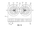
16 外側リング
20 第1の光電子装置用開口
22 第2の光電子装置用開口
24 第1の電子装置用開口
26 第2の電子装置用開口
30、32 面取りエッジ
34、36、40 直線縁取り部分
42 プリント回路基板
44 電気接点
46 導体パッド
56 第1の光電子装置
58 第2の光電子装置
Claims (22)
- 1つ以上のレンズを1つ以上の光電子装置に位置合わせするための方法であって、
ベース及び外側リングを備えたほぼ円筒形の筐体を有するアライナー装置を提供し、ここで、該ベースは、第1の光電子装置用開口と第2の光電子装置用開口とを有しており、該第1の光電子装置用開口は、ほぼ円形の形状を有し、前記外側リングと同軸であり、及び前記アライナー装置の中心軸と同軸であり、
前記第1の光電子装置用開口の中に第1の光電子装置を配置し、及び前記第2の光電子装置用開口の中に第2の光電子装置を配置し、ここで、該第1の光電子装置は、前記第1の光電子装置用開口の中においてトランジショナル嵌合を提供する寸法の周辺部を有しており、前記第1の光電子装置用開口の周辺部は、アライメント面を提供し、前記第1の光電子装置用開口の該アライメント面は、前記第1の光電子装置を前記中心軸に対して位置合わせし、且つ、前記第1の光電子装置を前記アライナー装置に対して前記中心軸から離れて動かないように保持し、及び、
前記アライナー装置の前記外側リングに光学装置を嵌合し、ここで、前記光学装置と外側リングとが嵌合アライメント面を有しており、該嵌合アライメント面は、前記光学装置を前記光電子装置に位置合わせし、且つ、前記光学装置を前記アライナー装置に対して動かないように保持する
ことを含み、
前記光学装置を嵌合することが、レンズ装置を嵌合することを含み、該レンズ装置が、第1のレンズと第2のレンズとを含み、及び、
前記レンズ装置及び前記外側リングの前記嵌合アライメント面が、前記第1のレンズを前記第1の光電子装置に位置合わせし、及び前記第2のレンズを前記第2の光電子装置に位置合わせすることからなる、方法。 - 前記第2の光電子装置用開口が、ほぼ円形の形状を有している、請求項1に記載の方法。
- 前記第2の光電子装置は、前記第2の光電子装置用開口の中においてトランジショナル嵌合を提供する寸法の周辺部を有している、請求項1又は2に記載の方法。
- 前記アライナー装置を提供することが、前記第1の光電子装置用開口の中に形成された直線縁取り部分を有するアライナー装置を提供して、前記アライナー装置に対して回転動作しないように前記第1の光電子装置を保持することを含むことからなる、請求項1に記載の方法。
- 前記アライナー装置を提供することが、
円筒形部分を有する成形型を形成し、
前記第1の光電子装置用開口及び前記外側リングに対応するモールド機構を形成するために、旋盤上において前記成形型の前記円筒形部分を回転させ、及び、
前記成形型を用いて、前記アライナー装置の前記筐体を成形する
ことを含むことからなる、請求項1に記載の方法。 - 前記旋盤上において前記円筒形部分を回転させることが、ダイヤモンドを回転させることを含むことからなる、請求項1に記載の方法。
- 前記アライナー装置を提供することが、面取りされたエッジを有した中心円形開口を有するアライナー装置を提供することを含み、及び、
前記第1の光電子装置を前記第1の光電子装置用開口の中に配置することは、前記面取りされたエッジが、前記第1の光電子装置を前記第1の光電子装置用開口内へと導くことを含むことからなる、請求項1に記載の方法。 - 前記アライナー装置を提供することが、前記筐体のベース内に第1の電子装置用開口を更に有するアライナー装置を提供することを含み、及び、
請求項1に記載の方法が、前記第1の電子装置用開口の中に第1の電子装置を配置することを更に含むことからなる、請求項1に記載の方法。 - 前記アライナー装置を提供することが、前記筐体のベース内に第2の電子装置用開口を更に有するアライナー装置を提供することを含み、及び、
請求項8に記載の方法が、前記第2の電子装置用開口の中に第2の電子装置を配置することを更に含むことからなる、請求項8に記載の方法。 - 前記アライナー装置をほぼ平面の基板に取り付け、及び、
前記第1の光電子装置を前記基板に取り付ける
ことを更に含むことからなる、請求項1に記載の方法。 - 前記基板がプリント回路基板を含む、請求項10に記載の方法。
- 前記アライナー装置を提供することが、2つ以上の直線縁取り部分を含む前記第1の光電子装置用開口を有するアライナー装置を提供することを含むことからなる、請求項2に記載の方法。
- 1つ以上のレンズを1つ以上の光電子装置に位置合わせするための方法であって、
ベース及び外側リングを備えたほぼ円筒形の筐体を有するアライナー装置を提供し、ここで、該ベースは、第1の光電子装置用開口及び第2の光電子装置用開口を有しており、該第1の光電子装置用開口は、ほぼ円形の形状を有し、前記外側リングと同軸であり、且つ、前記アライナー装置の中心軸と同軸であり、
前記第1の光電子装置用開口の中にほぼ四角形の形状を有した第1の光電子装置を配置し、ここで、該第1の光電子装置は、前記第1の光電子装置用開口の中においてトランジショナル嵌合を提供する寸法の周辺部を有しており、前記第1の光電子装置用開口の周辺部は、アライメント面を提供し、前記第1の光電子装置用開口の該アライメント面は、前記第1の光電子装置を前記中心軸に対して位置合わせし、且つ、前記第1の光電子装置を前記アライナー装置に対して前記中心軸から離れて動かないように保持し、
前記第2の光電子装置用開口の中にほぼ四角形の形状を有した第2の光電子装置を配置し、ここで、該第2の光電子装置は、前記第2の光電子装置用開口の中においてトランジショナル嵌合を提供する寸法の周辺部を有しており、前記第2の光電子装置用開口の周辺部は、アライメント面を提供し、前記第2の光電子装置用開口の該アライメント面は、前記第2の光電子装置を前記中心軸に対して位置合わせし、
前記アライナー装置の前記外側リングにレンズ装置を嵌合し、ここで、該レンズ装置は、第1のレンズ及び第2のレンズを含み、前記レンズ装置及び外側リングは、前記第1のレンズを前記第1の光電子装置に位置合わせするための、及び前記第2のレンズを前記第2の光電子装置に位置合わせするための、嵌合アライメント面を有しており、該嵌合アライメント面は、前記レンズ装置を前記アライナー装置に対して動かないように保持し、
前記アライナー装置をほぼ平面の基板に取り付け、
前記第1の光電子装置を前記基板に取り付け、及び、
前記第2の光電子装置を前記基板に取り付ける
ことを含む、方法。 - 前記アライナー装置を提供することが、前記筐体のベース内に第1の電子装置用開口を更に有するアライナー装置を提供することを含み、及び、
請求項13に記載の方法が、前記第1の電子装置用開口の中に第1の電子装置を配置することを更に含むことからなる、請求項13に記載の方法。 - 前記アライナー装置を提供することが、前記筐体のベース内に第2の電子装置用開口を更に有するアライナー装置を提供することを含み、及び、
請求項14に記載の方法が、前記第2の電子装置用開口の中に第2の電子装置を配置することを更に含むことからなる、請求項14に記載の方法。 - 1つ以上の光電子装置に位置合わせされる1つ以上のレンズを有するシステムであって、
ほぼ平面の基板と、
ベース及び外側リングを有したほぼ円筒形の筐体を有するアライナー装置であって、前記ベースは、前記基板上に実装されており、前記ベースは、第1の光電子装置用開口と第2の光電子装置用開口とを有しており、該第1の光電子装置用開口は、ほぼ円形の形状を有し、前記外側リングと同軸であり、且つ前記アライナー装置の中心軸と同軸であることからなる、アライナー装置と、
前記第1の光電子装置用開口の中の前記基板上に実装された第1の光電子装置であって、前記第1の光電子装置は、前記第1の光電子装置用開口の中においてトランジショナル嵌合を提供する寸法の周辺部を有しており、前記第1の光電子装置用開口の周辺部は、アライメント面を提供し、前記第1の光電子装置用開口の該アライメント面は、前記第1の光電子装置を前記中心軸に対して位置合わせすることからなる、第1の光電子装置と、
前記第2の光電子装置用開口の中の前記基板上に実装された第2の光電子装置と、
前記アライナー装置の前記外側リングに装着されたレンズ装置であって、該レンズ装置は、第1及び第2のレンズを含み、前記レンズ装置及び前記外側リングは、前記第1のレンズを前記第1の光電子装置に位置合わせするための、及び前記第2のレンズを前記第2の光電子装置に位置合わせするための、嵌合アライメント面を有することからなる、レンズ装置
とを備える、システム。 - 前記第2の光電子装置用開口は、ほぼ円形の形状を有しており、及び、
前記第2の光電子装置は、前記第2の光電子装置用開口の中においてトランジショナル嵌合を提供する寸法の周辺部を有していることからなる、請求項16に記載のシステム。 - 前記アライナー装置の前記第1の光電子装置用開口が、面取りされたエッジを有することからなる、請求項16に記載のシステム。
- 前記アライナー装置の前記第1の光電子装置用開口の周辺部が、1つ以上の直線縁取り部分を含むことからなる、請求項16に記載のシステム。
- 前記基板が、プリント回路基板を含む、請求項16に記載のシステム。
- 前記アライナー装置が、前記筐体のベース内に第1の電子装置用開口を有し、及び、前記基板に装着された第3の開口の中に第1の電子装置を更に含むことからなる、請求項16に記載のシステム。
- 前記アライナー装置が、前記筐体のベース内に第2の電子装置用開口を有し、及び、前記基板に装着された第4の開口の中に第2の電子装置を更に含むことからなる、請求項21に記載のシステム。
Applications Claiming Priority (2)
| Application Number | Priority Date | Filing Date | Title |
|---|---|---|---|
| US12/817,008 US8260097B2 (en) | 2010-06-16 | 2010-06-16 | Opto-electronic alignment system and method |
| US12/817,008 | 2010-06-16 |
Publications (3)
| Publication Number | Publication Date |
|---|---|
| JP2012009852A JP2012009852A (ja) | 2012-01-12 |
| JP2012009852A5 JP2012009852A5 (ja) | 2012-10-04 |
| JP5385336B2 true JP5385336B2 (ja) | 2014-01-08 |
Family
ID=45328744
Family Applications (1)
| Application Number | Title | Priority Date | Filing Date |
|---|---|---|---|
| JP2011121404A Expired - Fee Related JP5385336B2 (ja) | 2010-06-16 | 2011-05-31 | 光電子位置合わせシステム及び方法 |
Country Status (2)
| Country | Link |
|---|---|
| US (1) | US8260097B2 (ja) |
| JP (1) | JP5385336B2 (ja) |
Families Citing this family (13)
| Publication number | Priority date | Publication date | Assignee | Title |
|---|---|---|---|---|
| US9066456B2 (en) * | 2011-02-28 | 2015-06-23 | Avago Technologies General Ip (Singapore) Pte. Ltd. | Lens device attachment to printed circuit board |
| WO2013155263A1 (en) * | 2012-04-11 | 2013-10-17 | Ultra Communications, Inc. | Small form factor transceiver compatible with solder processing |
| CN103424823B (zh) * | 2012-05-22 | 2016-12-14 | 鸿富锦精密工业(深圳)有限公司 | 光电转换装置 |
| US9497860B2 (en) | 2012-11-07 | 2016-11-15 | Lattice Semiconductor Corporation | Methods and Apparatuses to provide an electro-optical alignment |
| CN103852836B (zh) * | 2012-11-29 | 2018-01-19 | 江苏地北网络工程有限公司 | 光电转换装置 |
| US9125299B2 (en) * | 2012-12-06 | 2015-09-01 | Apple Inc. | Cooling for electronic components |
| US9223167B2 (en) | 2013-06-26 | 2015-12-29 | Apple Inc. | Liquid crystal switching barrier thermal control |
| US9389029B2 (en) | 2013-09-30 | 2016-07-12 | Apple Inc. | Heat transfer structure |
| JP6576665B2 (ja) * | 2015-04-01 | 2019-09-18 | 新光電気工業株式会社 | 光素子用パッケージ及び光素子装置 |
| US9674986B2 (en) | 2015-08-03 | 2017-06-06 | Apple Inc. | Parallel heat spreader |
| US10077896B2 (en) | 2015-09-14 | 2018-09-18 | Trent Neil Butcher | Lighting devices including at least one light-emitting device and systems including at least one lighting device |
| KR101925476B1 (ko) * | 2015-11-25 | 2018-12-05 | 주식회사 옵텔라 | 광학 모듈 및 이를 포함하는 광학 엔진 |
| US20210050922A1 (en) * | 2019-08-14 | 2021-02-18 | Prime World International Holdings Ltd. | Method of bonding optical components of optical transceiver |
Family Cites Families (43)
| Publication number | Priority date | Publication date | Assignee | Title |
|---|---|---|---|---|
| JPH085872A (ja) * | 1994-06-23 | 1996-01-12 | Sumitomo Electric Ind Ltd | 光モジュール及びその製造方法 |
| JP3495821B2 (ja) * | 1995-06-08 | 2004-02-09 | キヤノン株式会社 | 光源装置 |
| JPH0990176A (ja) * | 1995-09-27 | 1997-04-04 | Nippon Telegr & Teleph Corp <Ntt> | 半導体光素子モジュール |
| US5841562A (en) * | 1995-12-28 | 1998-11-24 | Lucent Technologies, Inc. | Bidirectional modular optoelectronic transceiver assembly |
| US6550983B1 (en) * | 1996-01-18 | 2003-04-22 | Stratos Lightwave Llc | Optical package with alignment means and method of assembling an optical package |
| US6283644B1 (en) * | 1996-01-18 | 2001-09-04 | Stratos Lightwave, Inc. | Optical package with alignment means and method of assembling an optical package |
| US5812717A (en) * | 1996-01-18 | 1998-09-22 | Methode Electronics, Inc. | Optical package with alignment means and method of assembling an optical package |
| US5963684A (en) * | 1997-02-13 | 1999-10-05 | Lucent Technologies Inc. | Multiple-wavelength optical transceiver |
| US6597713B2 (en) * | 1998-07-22 | 2003-07-22 | Canon Kabushiki Kaisha | Apparatus with an optical functional device having a special wiring electrode and method for fabricating the same |
| US6845118B1 (en) * | 1999-01-25 | 2005-01-18 | Optical Communication Products, Inc. | Encapsulated optoelectronic devices with controlled properties |
| US6302596B1 (en) * | 1999-07-07 | 2001-10-16 | International Business Machines Corporation | Small form factor optoelectronic transceivers |
| US6540412B2 (en) * | 2000-02-10 | 2003-04-01 | Sumitomo Electric Industries, Ltd. | Optical transceiver |
| US6416238B1 (en) * | 2000-08-07 | 2002-07-09 | Stratos Lightwave, Inc. | Modular high density multiple optical transmitter/receiver array |
| US6892444B1 (en) | 2000-09-21 | 2005-05-17 | Axsun Technologies, Inc. | Optical system manufacturing and alignment system |
| JP4095283B2 (ja) * | 2000-12-06 | 2008-06-04 | キヤノン株式会社 | レーザ装置 |
| US6445858B1 (en) | 2000-12-11 | 2002-09-03 | Jds Uniphase Inc. | Micro-alignment of optical components |
| US6736553B1 (en) | 2001-01-12 | 2004-05-18 | Optical Communication Products, Inc. | VCSEL array optical subassembly module with alignment mechanism |
| JP2002261265A (ja) * | 2001-03-06 | 2002-09-13 | Sumitomo Electric Ind Ltd | 光通信装置 |
| JP3775480B2 (ja) * | 2001-03-13 | 2006-05-17 | セイコーエプソン株式会社 | 光モジュールの製造方法 |
| US6873799B2 (en) * | 2001-06-20 | 2005-03-29 | Jds Uniphase Corporation | Optical subassembly for optical communications |
| JP3782722B2 (ja) * | 2001-11-30 | 2006-06-07 | シャープ株式会社 | 光送受信モジュールおよび電子機器 |
| US6954592B2 (en) * | 2002-01-24 | 2005-10-11 | Jds Uniphase Corporation | Systems, methods and apparatus for bi-directional optical transceivers |
| US6939058B2 (en) * | 2002-02-12 | 2005-09-06 | Microalign Technologies, Inc. | Optical module for high-speed bidirectional transceiver |
| WO2003077002A1 (de) * | 2002-03-08 | 2003-09-18 | Infineon Technologies Ag | Aufnahme- und koppelteil für ein opto-elektronisches sende- und/oder empfangselement |
| JP3937911B2 (ja) * | 2002-05-10 | 2007-06-27 | 住友電気工業株式会社 | 光送受信モジュール及びこれを用いた光通信システム |
| JP2004086137A (ja) * | 2002-07-01 | 2004-03-18 | Seiko Epson Corp | 光トランシーバ及びその製造方法 |
| US7061949B1 (en) * | 2002-08-16 | 2006-06-13 | Jds Uniphase Corporation | Methods, apparatus, and systems with semiconductor laser packaging for high modulation bandwidth |
| JP2004095994A (ja) * | 2002-09-03 | 2004-03-25 | Canon Inc | 光源装置 |
| US6792171B2 (en) * | 2002-11-15 | 2004-09-14 | Jds Uniphase Corporation | Receiver optical sub-assembly |
| US6900509B2 (en) * | 2003-09-19 | 2005-05-31 | Agilent Technologies, Inc. | Optical receiver package |
| US6851870B1 (en) * | 2003-12-22 | 2005-02-08 | E-Pin Optical Industry Co., Ltd. | Method for measuring and assembling transceiver optical sub-assembly |
| US7056034B2 (en) * | 2003-12-30 | 2006-06-06 | Finisar Corporation | Passive alignment of laser with lens assembly |
| US7322754B2 (en) * | 2004-02-11 | 2008-01-29 | Jds Uniphase Corporation | Compact optical sub-assembly |
| US7223619B2 (en) | 2004-03-05 | 2007-05-29 | Avago Technologies Fiber Ip (Singapore) Pte. Ltd. | VCSEL with integrated lens |
| US7264408B2 (en) * | 2004-04-28 | 2007-09-04 | Finisar Corporation | Modular optical device package |
| GB2413840B (en) * | 2004-05-07 | 2006-06-14 | Savage Marine Ltd | Underwater lighting |
| US20060088255A1 (en) * | 2004-10-22 | 2006-04-27 | Enboa Wu | Multi-wavelength optical transceiver subassembly module |
| JP2007073664A (ja) * | 2005-09-06 | 2007-03-22 | Fuji Xerox Co Ltd | 光送受信モジュールおよび光通信装置 |
| JP2007078844A (ja) * | 2005-09-12 | 2007-03-29 | Fuji Xerox Co Ltd | 光送受信装置 |
| US20070051877A1 (en) * | 2005-09-06 | 2007-03-08 | Fuji Xerox Co., Ltd. | Optical transmitter-receiver, optical transmitter-receiver module, and optical communication device |
| CN101852349B (zh) * | 2005-12-22 | 2012-08-29 | 松下电器产业株式会社 | 具有led的照明器具 |
| US7344318B2 (en) | 2006-03-22 | 2008-03-18 | Intel Corporation | Optical interconnect with passive optical alignment |
| US8523458B2 (en) * | 2010-03-19 | 2013-09-03 | Corning Incorporated | Fiber optic interface device with bent optical path |
-
2010
- 2010-06-16 US US12/817,008 patent/US8260097B2/en active Active
-
2011
- 2011-05-31 JP JP2011121404A patent/JP5385336B2/ja not_active Expired - Fee Related
Also Published As
| Publication number | Publication date |
|---|---|
| US8260097B2 (en) | 2012-09-04 |
| US20110311182A1 (en) | 2011-12-22 |
| JP2012009852A (ja) | 2012-01-12 |
Similar Documents
| Publication | Publication Date | Title |
|---|---|---|
| JP5385336B2 (ja) | 光電子位置合わせシステム及び方法 | |
| JP6162114B2 (ja) | 光電子モジュール、光電子モジュールの製造方法、ならびに光電子モジュールを備える機器およびデバイス | |
| JP6328813B2 (ja) | リフロー可能な光電子モジュール | |
| JP5362003B2 (ja) | ファイバーカップリングを有するモールドオプチカルパッケージ | |
| KR101432399B1 (ko) | 발광 장치 및 그 제조 방법 | |
| US20140291703A1 (en) | Opto-Electronic Module | |
| EP2581776A1 (en) | Optical connector with alignment element, optical unit and assembly method | |
| TW202033937A (zh) | 用來產生光圖案之照明投影器模組及製造照明投影器模組之方法 | |
| JP2015161909A (ja) | 光伝送モジュール及び光伝送モジュールの製造方法 | |
| US9435966B2 (en) | Lens device attachment to printed circuit board | |
| CN108027483A (zh) | 部件对准 | |
| EP2541575B1 (en) | Method for fixing lens section in optical sensor and optical sensor | |
| JP2000241696A (ja) | 光学センサーパッケージの保持・取付け方法 | |
| US7371652B2 (en) | Alignment using fiducial features | |
| TWM470270U (zh) | 光次模組 | |
| US7093986B2 (en) | Low cost optical module | |
| KR20070113651A (ko) | 수동 정렬된 광결합 장치 및 그 제작방법 | |
| TWI475276B (zh) | 光次模組及其封裝方法 | |
| JP2005340770A (ja) | 電光変換モジュール及び光電変換モジュール | |
| JP2009134320A (ja) | 光モジュールの製造方法 | |
| JP7206860B2 (ja) | レンズユニット、対象物検出装置 | |
| JP2000322989A (ja) | 光電センサ並びにその製造方法 | |
| JP4467656B2 (ja) | 焦点検出装置及び位置調整方法 | |
| US20150372757A1 (en) | Aligning optical elements of an optical transceiver system | |
| US10281664B1 (en) | Method for determining a spatial relationship between an optoelectronic chip and an optical mount |
Legal Events
| Date | Code | Title | Description |
|---|---|---|---|
| A521 | Request for written amendment filed |
Free format text: JAPANESE INTERMEDIATE CODE: A523 Effective date: 20120816 |
|
| A621 | Written request for application examination |
Free format text: JAPANESE INTERMEDIATE CODE: A621 Effective date: 20120816 |
|
| A977 | Report on retrieval |
Free format text: JAPANESE INTERMEDIATE CODE: A971007 Effective date: 20130610 |
|
| A711 | Notification of change in applicant |
Free format text: JAPANESE INTERMEDIATE CODE: A712 Effective date: 20130718 |
|
| A131 | Notification of reasons for refusal |
Free format text: JAPANESE INTERMEDIATE CODE: A131 Effective date: 20130723 |
|
| A521 | Request for written amendment filed |
Free format text: JAPANESE INTERMEDIATE CODE: A523 Effective date: 20130902 |
|
| TRDD | Decision of grant or rejection written | ||
| A01 | Written decision to grant a patent or to grant a registration (utility model) |
Free format text: JAPANESE INTERMEDIATE CODE: A01 Effective date: 20131001 |
|
| A61 | First payment of annual fees (during grant procedure) |
Free format text: JAPANESE INTERMEDIATE CODE: A61 Effective date: 20131003 |
|
| R150 | Certificate of patent or registration of utility model |
Free format text: JAPANESE INTERMEDIATE CODE: R150 |
|
| LAPS | Cancellation because of no payment of annual fees |