JP5365173B2 - Physical quantity measuring device and electronic device - Google Patents
Physical quantity measuring device and electronic device Download PDFInfo
- Publication number
- JP5365173B2 JP5365173B2 JP2008307619A JP2008307619A JP5365173B2 JP 5365173 B2 JP5365173 B2 JP 5365173B2 JP 2008307619 A JP2008307619 A JP 2008307619A JP 2008307619 A JP2008307619 A JP 2008307619A JP 5365173 B2 JP5365173 B2 JP 5365173B2
- Authority
- JP
- Japan
- Prior art keywords
- circuit
- drive
- physical quantity
- amplitude
- signal
- Prior art date
- Legal status (The legal status is an assumption and is not a legal conclusion. Google has not performed a legal analysis and makes no representation as to the accuracy of the status listed.)
- Expired - Fee Related
Links
Images


Classifications
-
- G—PHYSICS
- G01—MEASURING; TESTING
- G01C—MEASURING DISTANCES, LEVELS OR BEARINGS; SURVEYING; NAVIGATION; GYROSCOPIC INSTRUMENTS; PHOTOGRAMMETRY OR VIDEOGRAMMETRY
- G01C19/00—Gyroscopes; Turn-sensitive devices using vibrating masses; Turn-sensitive devices without moving masses; Measuring angular rate using gyroscopic effects
- G01C19/56—Turn-sensitive devices using vibrating masses, e.g. vibratory angular rate sensors based on Coriolis forces
- G01C19/5607—Turn-sensitive devices using vibrating masses, e.g. vibratory angular rate sensors based on Coriolis forces using vibrating tuning forks
Abstract
Description
本発明は、物理量測定装置(例えば、振動子の振動運動に対するコリオリ力を検出することで角速度を検出する振動型ジャイロスコープ)および電子機器等に関する。 The present invention relates to a physical quantity measuring device (for example, a vibrating gyroscope that detects an angular velocity by detecting a Coriolis force with respect to a vibrating motion of a vibrator), an electronic device, and the like.
振動型ジャイロスコープの構成例は、例えば、特許文献1に記載されている。特許文献1では、振動子に駆動振動を励振する発振駆動回路において、駆動振動の振幅を一定とするためのAGC回路(自動利得制御回路)を設けている。
特許文献1の振動型ジャイロスコープ(以下、ジャイロスコープという場合がある)では、上述のようにAGC回路により駆動振幅が一定に保たれるよう構成されているが、AGC回路による振幅一定化が達成されていない状態では、検出感度が一定しない。特に、発振起動時は、振幅が徐々に増大するため、感度が徐々に変化する。このため、従来のジャイロスコープでは、発振起動期間において得られる検出信号は無効とするしかなく、よって、所望の検出感度を得るための起動時間が長くなる。 The vibratory gyroscope of Patent Document 1 (hereinafter sometimes referred to as a gyroscope) is configured such that the drive amplitude is kept constant by the AGC circuit as described above, but the amplitude constant by the AGC circuit is achieved. In a state where it is not performed, the detection sensitivity is not constant. In particular, when the oscillation starts, the amplitude gradually increases, so that the sensitivity gradually changes. For this reason, in the conventional gyroscope, the detection signal obtained in the oscillation start-up period can only be invalidated, and therefore the start-up time for obtaining the desired detection sensitivity becomes long.
また、駆動振動の振幅は、種々の外乱(例えば、電源電圧の変動あるいはジャイロスコープに与えられる外からの衝撃等)によって変動する。AGC回路が設けられていても、外乱によって変動した振幅が所望レベルに収束するまでの期間においては、駆動振動の振幅の乱れが継続している。よって、その期間において、検出感度が変化する。 In addition, the amplitude of the drive vibration varies due to various disturbances (for example, a variation in power supply voltage or an external impact applied to the gyroscope). Even if the AGC circuit is provided, the disturbance of the amplitude of the drive vibration continues during the period until the amplitude changed by the disturbance converges to a desired level. Therefore, the detection sensitivity changes during that period.
例えば、ジャイロスコープをカメラの手振れ補正のために使用する場合、カメラにわずかな衝撃が加わっただけでも駆動振動の振幅が変化する。より高精度のジャイロスコープを実現しようとする場合、電源電圧の変動等の電気的な外乱要因に対する対策はもちろんのこと、機械的な外乱要因(電子機器に加わる衝撃や揺れ等)に対する対策も必要である。従来技術では、このような課題を解決することができない。 For example, when a gyroscope is used for camera shake correction, the amplitude of drive vibration changes even when a slight impact is applied to the camera. When implementing a gyroscope with higher accuracy, not only measures against electrical disturbance factors such as fluctuations in power supply voltage, but also measures against mechanical disturbance factors (such as impact and vibration applied to electronic devices) are required. It is. The conventional technique cannot solve such a problem.
本発明はこのような考察に基づいてなされたものである。本発明の幾つかの実施形態によれば、例えば、駆動振動の振幅が変動したとしても、検出しようとする物理量に対する検出感度を一定に保つことができ、高精度の検出が可能である。 The present invention has been made based on such consideration. According to some embodiments of the present invention, for example, even if the amplitude of the drive vibration varies, the detection sensitivity for the physical quantity to be detected can be kept constant, and high-precision detection is possible.
(1)本発明の物理量測定装置の一態様では、物理量トランスデューサと発振ループを形成し、前記物理量トランスデューサに駆動振動を励振する発振駆動回路と、前記物理量トランスデューサから出力されるアナログの検出信号を検波回路によって検波した後、検波された信号を、A/D変換器によってデジタル信号に変換して出力する検出回路と、を含み、前記発振駆動回路は、前記駆動振動の振幅を検出する駆動振幅検出回路を有し、前記検出回路に含まれる前記A/D変換器の基準電圧の電圧レベルは、前記駆動振幅検出回路の検出出力信号に基づいて制御される。 (1) In one aspect of the physical quantity measuring device of the present invention, an oscillation loop is formed with a physical quantity transducer, and an oscillation drive circuit that excites drive vibration in the physical quantity transducer, and an analog detection signal output from the physical quantity transducer is detected. A detection circuit that detects a signal detected by the circuit, converts the detected signal into a digital signal by an A / D converter, and outputs the digital signal. The oscillation drive circuit detects the amplitude of the drive vibration. A voltage level of a reference voltage of the A / D converter included in the detection circuit is controlled based on a detection output signal of the drive amplitude detection circuit.
例えば、物理量測定装置を用いて角速度を検出する場合、回転に伴って物理量トランスデューサとしての振動子に加わるコリオリ力Fは、F=2mvΩ(mは振動子の質量、vは振動子の速度、Ωは角速度)と表すことができる。振動子の駆動振動の振幅が変化すると、速度vが変化し、コリオリ力Fが変化してしまう。そこで、本態様では、駆動振動の振幅に対応させて、検出回路の出力段に設けられるA/D変換器の基準電圧(リファレンス)の電圧レベルを可変に(適応的に)制御し、駆動振幅が変動すると、A/D変換器の基準電圧(リファレンス)も、その変動に追従して変化するようにする。これによって、A/D変換器から出力されるコード(例えば、256階調のA/D変換器の場合、出力コードはコード0〜コード255のいずれかとなる)は一定に保たれる。よって、検出しようとする物理量の検出感度は、外乱に関係なく、常に一定に保たれる。すなわち、本態様では、振動子の駆動振動に対するレシオメトリック(駆動振幅の変動によって検出感度が変化しない新規なレシオメトリック構成)が実現される。 For example, when the angular velocity is detected using a physical quantity measuring device, the Coriolis force F applied to the vibrator as the physical quantity transducer with rotation is F = 2 mvΩ (m is the mass of the vibrator, v is the speed of the vibrator, Ω Can be expressed as angular velocity). When the amplitude of the drive vibration of the vibrator changes, the speed v changes and the Coriolis force F changes. Therefore, in this aspect, the voltage level of the reference voltage (reference) of the A / D converter provided in the output stage of the detection circuit is variably (adaptively) controlled in accordance with the amplitude of the drive vibration, and the drive amplitude Is changed, the reference voltage (reference) of the A / D converter is also changed following the change. As a result, the code output from the A / D converter (for example, in the case of a 256 gradation A / D converter, the output code is one of code 0 to code 255) is kept constant. Therefore, the detection sensitivity of the physical quantity to be detected is always kept constant regardless of the disturbance. That is, in this aspect, a ratiometric (a new ratiometric configuration in which the detection sensitivity does not change due to fluctuations in drive amplitude) with respect to the drive vibration of the vibrator is realized.
(2)本発明の物理量測定装置の他の態様では、前記A/D変換器の基準電圧の電圧レベルは、前記A/D変換器の変換幅が、前記駆動振動の振幅に比例するように制御される。 (2) In another aspect of the physical quantity measuring device of the present invention, the voltage level of the reference voltage of the A / D converter is such that the conversion width of the A / D converter is proportional to the amplitude of the driving vibration. Be controlled.
例えば、A/D変換器の基準電圧(リファレンス)として、VrefHとVrefLという2つの基準電圧が使用される場合を想定する。VrefHおよびVrefLで規定されるダイナミックレンジがA/D変換器の変換幅である。また、駆動振幅が変動する前の状態における検波回路の検出出力をVdetect1とし、変動後の状態における検出出力をVdetect2とする。このとき、本態様によれば、(VrefH−Vdetect1)に対する(Vdetect1−VrefL)の比と、(VrefH−Vdetect2)に対する(Vdetect2−VrefL)の比は同じになる。よって、A/D変換器から出力されるコードは、駆動振幅が変動しても同じであり、物理量の検出感度は一定に保たれる。 For example, it is assumed that two reference voltages VrefH and VrefL are used as the reference voltage (reference) of the A / D converter. The dynamic range defined by VrefH and VrefL is the conversion width of the A / D converter. Further, the detection output of the detection circuit in the state before the drive amplitude fluctuates is Vdetect1, and the detection output in the state after the fluctuation is Vdetect2. At this time, according to this aspect, the ratio of (Vdetect1-VrefL) to (VrefH-Vdetect1) is the same as the ratio of (Vdetect2-VrefL) to (VrefH-Vdetect2). Therefore, the code output from the A / D converter is the same even if the drive amplitude varies, and the detection sensitivity of the physical quantity is kept constant.
(3)本発明の物理量測定装置の他の態様では、前記発振駆動回路は、前記駆動振動の振幅を一定にするためのAGC回路を有し、前記駆動振幅検出回路は、前記AGC回路を構成する回路の一つである。 (3) In another aspect of the physical quantity measuring device of the present invention, the oscillation drive circuit has an AGC circuit for making the amplitude of the drive vibration constant, and the drive amplitude detection circuit constitutes the AGC circuit. It is one of the circuits that do.
発振駆動回路にAGC回路が搭載される場合、AGC回路には、駆動振動の振幅(発振ループの発振振幅)を検出するための駆動振幅検出回路が必然的に設けられる。この駆動振幅検出回路の検出信号を、A/D変換器の基準電圧(リファレンス)の制御のために流用することによって、新規に駆動振幅検出回路を設ける必要がなくなる。よって、回路の占有面積の増大が生じない。 When the AGC circuit is mounted on the oscillation drive circuit, the AGC circuit is inevitably provided with a drive amplitude detection circuit for detecting the amplitude of the drive vibration (oscillation amplitude of the oscillation loop). By using the detection signal of the drive amplitude detection circuit for the control of the reference voltage (reference) of the A / D converter, there is no need to newly provide a drive amplitude detection circuit. Therefore, the area occupied by the circuit does not increase.
(4)本発明の物理量測定装置の他の態様では、前記駆動振幅検出回路の検出出力信号および前記検出出力信号の電圧レベルを反転した信号の少なくとも一方が、前記A/D変換器の前記基準電圧として使用される。 (4) In another aspect of the physical quantity measuring device of the present invention, at least one of the detection output signal of the drive amplitude detection circuit and the signal obtained by inverting the voltage level of the detection output signal is the reference of the A / D converter. Used as voltage.
駆動振幅検出回路の検出出力信号(もしくは、その電圧レベルを反転した信号)を、そのままA/D変換器の基準電圧として使用することができる。A/D変換器の基準電圧が2つあり(VrefHとVrefL)、その2つの基準電圧の各々を適応的に変化させる場合は、駆動振幅検出回路の検出出力信号と、その電圧レベルを反転した信号の各々を、基準電圧VrefHおよびVrefLとして使用することができる。A/D変換器の2つの基準電圧のうちのいずれか一方(VrefHあるいはVrefL)を適応的に変化させる場合は、駆動振幅検出回路の検出出力信号またはその電圧レベルを反転した信号のいずれかを、基準電圧VrefHまたはVrefLとして使用することができる。 The detection output signal of the drive amplitude detection circuit (or a signal obtained by inverting the voltage level) can be used as it is as the reference voltage of the A / D converter. When there are two A / D converter reference voltages (VrefH and VrefL) and each of the two reference voltages is adaptively changed, the detection output signal of the drive amplitude detection circuit and its voltage level are inverted. Each of the signals can be used as reference voltages VrefH and VrefL. When either one of the two reference voltages (VrefH or VrefL) of the A / D converter is adaptively changed, either the detection output signal of the drive amplitude detection circuit or a signal obtained by inverting the voltage level is used. , And can be used as the reference voltage VrefH or VrefL.
(5)本発明の物理量測定装置の他の態様では、前記駆動振幅検出回路の検出出力信号の電圧レベルを調整することによって得られる信号を第1の信号とし、前記第1の信号の電圧レベルを反転した信号を第2の信号とした場合、前記第1の信号および前記第2の信号の少なくとも一方が、前記A/D変換器の前記基準電圧として使用される。 (5) In another aspect of the physical quantity measuring device of the present invention, a signal obtained by adjusting the voltage level of the detection output signal of the drive amplitude detection circuit is defined as the first signal, and the voltage level of the first signal When the signal obtained by inverting is used as the second signal, at least one of the first signal and the second signal is used as the reference voltage of the A / D converter.
駆動振動に対するレシオメトリックを実現する上で、検出出力信号の電圧レベルの調整が必要となる場合がある。例えば、所定の増幅率をもつアンプ(あるいは可変ゲインアンプ)を用いて駆動振幅検出回路の検出信号を増幅し、これによって電圧レベルを調整(増減)することができる。 In order to realize the ratio metric with respect to the driving vibration, it may be necessary to adjust the voltage level of the detection output signal. For example, it is possible to amplify the detection signal of the drive amplitude detection circuit using an amplifier (or a variable gain amplifier) having a predetermined amplification factor, thereby adjusting (increasing or decreasing) the voltage level.
(6)本発明の物理量測定装置の他の態様では、前記検出回路は、前記駆動振幅検出回路の検出出力信号に重畳されるオフセット電圧を補償するためのオフセット調整回路を有する。 (6) In another aspect of the physical quantity measuring device of the present invention, the detection circuit includes an offset adjustment circuit for compensating for an offset voltage superimposed on a detection output signal of the drive amplitude detection circuit.
発振駆動回路(および検出回路)の信号経路の基準バイアス電圧AGND(アナロググランド:例えば、AGND=VDD/2)に、オフセット電圧(アンプやトランジスタの特性変動等、種々の要因によって発生する)が重畳されると、そのオフセット電圧は、振動子の駆動振動に対するレシオメトリックを実現する上での誤差の原因となる。そこで、オフセット調整回路を設けて、オフセット電圧を補償するものである。これによって、駆動振幅検出回路の検出出力にオフセットが重畳されている場合でも、検出感度の変動が生じない。 An offset voltage (generated due to various factors such as amplifier and transistor characteristic fluctuations) is superimposed on the reference bias voltage AGND (analog ground: for example, AGND = VDD / 2) of the signal path of the oscillation drive circuit (and detection circuit). Then, the offset voltage causes an error in realizing the ratiometric with respect to the driving vibration of the vibrator. Therefore, an offset adjustment circuit is provided to compensate for the offset voltage. Thereby, even when an offset is superimposed on the detection output of the drive amplitude detection circuit, the detection sensitivity does not vary.
(7)本発明の物理量測定装置の他の態様では、前記駆動振幅検出回路は、前記発振ループの発振信号を整流する整流回路と、前記整流回路の出力信号を平滑する平滑回路と、を有する。 (7) In another aspect of the physical quantity measuring device of the present invention, the drive amplitude detection circuit includes a rectifier circuit that rectifies an oscillation signal of the oscillation loop, and a smoothing circuit that smoothes an output signal of the rectifier circuit. .
この構成によって、駆動振動の振幅に対応した電圧信号を生成することができる。 With this configuration, a voltage signal corresponding to the amplitude of the drive vibration can be generated.
(8)本発明の物理量測定装置の他の態様では、前記駆動振幅検出回路は、前記発振ループの発振信号を整流する整流回路と、整流した信号を積分する積分回路とが一体化された整流・積分回路により構成される。 (8) In another aspect of the physical quantity measuring device of the present invention, the drive amplitude detection circuit is a rectifier in which a rectifier circuit that rectifies an oscillation signal of the oscillation loop and an integration circuit that integrates the rectified signal are integrated. -Consists of an integration circuit.
この構成によって、駆動振幅検出回路の回路構成を簡素化することができる。回路の占有面積の低減が可能である。 With this configuration, the circuit configuration of the drive amplitude detection circuit can be simplified. The area occupied by the circuit can be reduced.
(9)本発明の物理量測定装置の他の態様では、前記発振駆動回路は、前記駆動振動の振幅を一定にするにするためのAGC回路に代わりに設けられる、前記駆動振動の振幅の上限および下限の少なくとも一方を規制するための振幅制限回路を有する。 (9) In another aspect of the physical quantity measuring device of the present invention, the oscillation drive circuit is provided in place of an AGC circuit for making the amplitude of the drive vibration constant, and an upper limit of the amplitude of the drive vibration and It has an amplitude limiting circuit for regulating at least one of the lower limits.
上述のとおり、本発明の各態様の物理量測定装置では、駆動振幅が変動しても、A/D変換器の基準電圧(リファレンス)も、その変動に追従して変化し、物理量の検出感度は、外乱に関係なく一定に保たれる。そこで、発振駆動回路において、AGC回路に代えて、振幅制限回路(振幅リミッタ)を設けるという簡易な回路構成(つまり、駆動振動の振幅の変動幅の最大値を、所定レベル以下に抑制するだけの回路構成)を採用する。これによって、発振駆動回路の占有面積の低減ならびに消費電力の削減を図ることができる。 As described above, in the physical quantity measuring device of each aspect of the present invention, even if the drive amplitude varies, the reference voltage (reference) of the A / D converter also changes following the fluctuation, and the detection sensitivity of the physical quantity is , Kept constant regardless of disturbance. Therefore, in the oscillation drive circuit, a simple circuit configuration in which an amplitude limiting circuit (amplitude limiter) is provided in place of the AGC circuit (that is, the maximum value of the fluctuation range of the amplitude of the drive vibration is suppressed to a predetermined level or less. Circuit configuration). As a result, it is possible to reduce the area occupied by the oscillation drive circuit and the power consumption.
(10)本発明の電子機器の一態様は、上記の物理量測定装置と、前記物理量測定装置と同時に動作する可動機構と、を含む。 (10) One aspect of the electronic device of the present invention includes the physical quantity measuring device described above and a movable mechanism that operates simultaneously with the physical quantity measuring device.
本発明の物理量測定装置は、外乱に関係なく物理量の検出感度を一定に保つことができるため、発振起動期間(電源投入時点から発振定常状態に至るまでの期間)においても、有効な物理量の検出信号を得ることができ、よって、電子機器の起動待ち時間を短縮できる。また、電源電圧の変動等の電気的な外乱要因に対する対策ならびに機械的な外乱要因(電子機器に加わる衝撃や揺れ等)に対する対策も実現される。更に、電子機器が、本発明の物理量測定装置と同時に動作する可動機構を持つ場合、可動機構からの振動や衝撃の影響を排除できる。よって、電子機器の性能が向上する。 Since the physical quantity measuring device of the present invention can keep the detection sensitivity of a physical quantity constant regardless of disturbances, it can detect an effective physical quantity even during the oscillation start-up period (period from when the power is turned on to the oscillation steady state). A signal can be obtained, and thus the activation waiting time of the electronic device can be shortened. In addition, measures against electrical disturbance factors such as fluctuations in the power supply voltage and measures against mechanical disturbance factors (such as impact and vibration applied to the electronic device) can be realized. Furthermore, when the electronic apparatus has a movable mechanism that operates simultaneously with the physical quantity measuring device of the present invention, it is possible to eliminate the influence of vibration and impact from the movable mechanism. Therefore, the performance of the electronic device is improved.
このように、本発明の幾つかの実施形態によれば、例えば、駆動振動の振幅が変動したとしても、検出しようとする物理量に対する検出感度を一定に保つことができ、高精度の検出が可能である。 As described above, according to some embodiments of the present invention, for example, even when the amplitude of the drive vibration fluctuates, the detection sensitivity for the physical quantity to be detected can be kept constant, and high-precision detection is possible. It is.
(11)本発明の物理量測定装置の他の態様は、上記いずれかの物理量測定装置は振動型ジャイロスコープであり、前記物理量トランスデューサは、前記発振駆動回路によって駆動振動が励振されると共に、角速度に応じた振幅の検出信号を生成する振動型ジャイロスコープ素子である。 (11) In another aspect of the physical quantity measuring device of the present invention, any one of the above physical quantity measuring devices is a vibration type gyroscope, and the physical quantity transducer is driven by the oscillation driving circuit and driven at an angular velocity. It is a vibration type gyroscope element that generates a detection signal having a corresponding amplitude.
これによって、電源電圧の変動等の電気的な外乱要因に対する対策ならびに機械的な外乱要因(電子機器に加わる衝撃や揺れ等)に対する対策がなされた、高精度の測定が可能な振動型ジャイロスコープが実現される。 As a result, a vibratory gyroscope capable of high-accuracy measurement with measures against electrical disturbance factors such as power supply voltage fluctuations and mechanical disturbance factors (such as shocks and vibrations applied to electronic devices) has been developed. Realized.
(12)本発明の電子機器の他の態様は、上記いずれかの物理量測定装置と、可動機構と、を含み、前記物理量測定装置の動作期間と前記可動機構の動作期間が重なりを有する。 (12) Another aspect of the electronic apparatus of the present invention includes any one of the physical quantity measurement devices described above and a movable mechanism, and the operation period of the physical quantity measurement device overlaps the operation period of the movable mechanism.
電子機器に含まれる可動機構の動作期間が、物理量測定装置の動作期間と重なりを有している場合であっても、可動機構からの振動や衝撃の影響によって、物理量測定装置の測定精度が低下するという不都合が生じない。よって、電子機器の性能が向上する。 Even if the operation period of the movable mechanism included in the electronic device overlaps with the operation period of the physical quantity measurement device, the measurement accuracy of the physical quantity measurement device decreases due to the influence of vibration and impact from the movable mechanism. Inconvenience does not occur. Therefore, the performance of the electronic device is improved.
(13)本発明の電子機器の他の態様では、前記可動機構は、機械的な可動構成要素を含む。 (13) In another aspect of the electronic apparatus of the invention, the movable mechanism includes a mechanical movable component.
機械的な可動要素を含む可動機構としては、例えば、カメラに設けられる機械的シャッター、一眼レフカメラに設けられるミラー跳ね上げ機構(またはクイックリターン機構)やオートフォーカス(AF)制御機構、あるいは家庭用のゲームコントローラに設けられるバイブレータ等が挙げられる。 As a movable mechanism including a mechanical movable element, for example, a mechanical shutter provided in a camera, a mirror flip-up mechanism (or quick return mechanism) or an autofocus (AF) control mechanism provided in a single-lens reflex camera, or a home use And a vibrator provided in the game controller.
(14)本発明の電子機器の他の態様では、前記可動機構は、衝撃を発生する衝撃源である。 (14) In another aspect of the electronic apparatus of the invention, the movable mechanism is an impact source that generates an impact.
例えば、カメラに設けられる機械的シャッターは瞬時的に開閉されるため、その開閉動作に伴い、機械的な衝撃が発生する。また、例えば、一眼レフカメラに設けられるミラー跳ね上げ機構(またはクイックリターン機構)は、ミラーを瞬時的に光軸上から退避させたり、あるいは元の位置に復帰させたりする動作を行うため、その動作に伴って機械的な衝撃が発生する。また、例えば、一眼レフカメラに設けられるオートフォーカス(AF)制御機構も、AFモータの駆動や駆動停止に伴って、機械的な衝撃を発生させる場合がある。したがって、可動機構は衝撃源となり得る。 For example, since a mechanical shutter provided in the camera is opened and closed instantaneously, a mechanical shock is generated with the opening and closing operation. Further, for example, a mirror flip-up mechanism (or quick return mechanism) provided in a single-lens reflex camera performs an operation of momentarily retracting the mirror from the optical axis or returning it to the original position. A mechanical shock occurs with the movement. In addition, for example, an autofocus (AF) control mechanism provided in a single-lens reflex camera may generate a mechanical shock when the AF motor is driven or stopped. Therefore, the movable mechanism can be an impact source.
カメラ(一眼レフカメラを含む)に、例えば、本発明のジャイロスコープが、手振れ補正のためにカメラ内に設けられる場合、そのジャイロスコープは、可動機構の動作によって発生する機械的な衝撃に影響されることなく、常に、高精度の角速度等の測定を実行することができる。よって、正確な手振れ補正が実現される。 When a gyroscope of the present invention is provided in a camera (including a single-lens reflex camera), for example, in a camera for camera shake correction, the gyroscope is affected by a mechanical impact generated by the operation of a movable mechanism. Therefore, it is possible to always measure the angular velocity with high accuracy. Therefore, accurate camera shake correction is realized.
(15)本発明の電子機器の他の態様では、前記可動機構は、振動を発生する振動源である。 (15) In another aspect of the electronic apparatus of the invention, the movable mechanism is a vibration source that generates vibration.
例えば、臨場感あふれるゲームを楽しむために、家庭用ゲームコントローラにバイブレータが内蔵される場合がある。バイブレータは、機械的な振動源である。例えば、本発明のジャイロスコープが、ゲームコントローラの姿勢検出のためにゲームコントローラ内に設けられる場合、そのジャイロスコープは、可動機構の動作によって発生する機械的な衝撃に影響されることなく、常に、高精度の角速度等の測定を実行することができる。よって、正確な姿勢検出が可能である。 For example, there is a case where a vibrator is built in a home game controller in order to enjoy a realistic game. The vibrator is a mechanical vibration source. For example, when the gyroscope of the present invention is provided in the game controller for detecting the attitude of the game controller, the gyroscope is always not affected by the mechanical impact generated by the operation of the movable mechanism, A highly accurate measurement of angular velocity or the like can be performed. Therefore, accurate posture detection is possible.
次に、本発明の実施形態について、図面を参照して説明する。なお、以下に説明する本実施形態は、特許請求の範囲に記載された本発明の内容を不当に限定するものではなく、本実施形態で説明される構成のすべてが、本発明の解決手段として必須であるとは限らない。 Next, embodiments of the present invention will be described with reference to the drawings. Note that the present embodiment described below does not unduly limit the contents of the present invention described in the claims, and all the configurations described in the present embodiment are as means for solving the present invention. It is not always essential.
(第1の実施形態)
まず、振動型ジャイロスコープの動作原理を説明する。振動型ジャイロスコープは、水晶あるいはセラミックなどで作成した圧電振動子や、シリコンなどで作成した静電駆動の振動子など(物理量トランスデューサ)を利用した角速度測定装置である。振動運動(駆動振動)をしている振動子に角速度を加えると、振動の方向と直交する向きにコリオリ力が働き、結果としてコリオリ力の方向に振動(検出振動)を始める。このコリオリ力による振動は、駆動振動と同じ周波数であり、振幅は入力された角速度に比例する。コリオリ力による振動(検出振動)の強さを測定することで、振動子にかかっている角速度を測定することができる。
(First embodiment)
First, the operation principle of the vibration gyroscope will be described. The vibratory gyroscope is an angular velocity measuring device using a piezoelectric vibrator made of crystal or ceramic, an electrostatically driven vibrator made of silicon or the like (physical quantity transducer). When an angular velocity is applied to a vibrator that performs vibrational motion (drive vibration), Coriolis force acts in a direction orthogonal to the vibration direction, and as a result, vibration (detection vibration) starts in the direction of Coriolis force. The vibration due to the Coriolis force has the same frequency as the driving vibration, and the amplitude is proportional to the input angular velocity. By measuring the strength of vibration (detected vibration) due to Coriolis force, the angular velocity applied to the vibrator can be measured.
図11は、振動型ジャイロスコープの動作原理を説明するための図である。振動型ジャイロスコープの振動子1として音叉型水晶振動子を用いた場合、この振動子1の表面の所定箇所には、励振用の駆動電極2及びコリオリ力検出用の検出電極3が設けられる。駆動電極2には、交流(AC)の駆動電圧を供給するための発振回路4が接続される。また、検出電極3には、検出回路5が接続される。
FIG. 11 is a diagram for explaining the operation principle of the vibration type gyroscope. When a tuning fork crystal resonator is used as the
振動子1は質量mを有し、駆動電極2に発振回路4からAC駆動電圧が印加されると、この振動子1がX軸に沿ってB方向に所定の周波数で振動する。Y軸の回りに角速度Ωが加わると、X軸と直交するZ軸方向にコリオリ力F(=2mvΩ)が発生する。但し、vは圧電振動子1の速度である。コリオリ力Fは角速度Ωの大きさに比例して定まることから、検出電極3及び検出回路5により、コリオリ力Fを圧電振動子1の撓み変位量として検出することで、この圧電振動子1の角速度Ωの大きさを求めることができる。
The
ここで、発振回路により駆動される振動子の速度vは、駆動振動の振幅a、駆動振動の角周波数ω0、時間tとして、v=a sinω0tと表すことができる。このことから、一定の角速度入力Ωに対するコリオリ力、ひいては検出信号を一定にするためには、駆動振動の振幅aを一定に保つ必要があることがわかる。(振幅が大きくなれば検出感度が高くなり、振幅が小さくなれば検出感度が低くなる)。また、検出出力は、駆動振動と同じ周波数で、角速度入力Ωに比例した振幅を持つ、いわば振幅変調波(AM)で出力されることがわかる。 Here, the speed v of the vibrator is driven by the oscillation circuit, the amplitude a of the driving vibration, the drive oscillation of the angular frequency omega 0, as the time t, can be expressed as v = a sinω 0 t. From this, it is understood that the amplitude a of the drive vibration needs to be kept constant in order to make the Coriolis force with respect to the constant angular velocity input Ω, and thus the detection signal constant. (The detection sensitivity increases as the amplitude increases, and the detection sensitivity decreases as the amplitude decreases). It can also be seen that the detection output is output as an amplitude-modulated wave (AM) having the same frequency as the drive vibration and an amplitude proportional to the angular velocity input Ω.
このことから、一般的な振動型ジャイロスコープの駆動・検出回路では、発振回路4は、発振振幅を一定にするための自動利得制御回路(Automatic Gain Control:AGC)回路を備え、駆動振動の振幅aを一定に保つ構成が採用される。 Therefore, in the drive / detection circuit of a general vibration type gyroscope, the oscillation circuit 4 includes an automatic gain control circuit (AGC) circuit for making the oscillation amplitude constant, and the amplitude of the drive vibration. A configuration is adopted in which a is kept constant.
(振動型ジャイロスコープの回路構成の一例)
図1は、振動型ジャイロスコープの基本的な構成の一例を示す図である。図1の振動型ジャイロスコープ(以下、ジャイロスコープあるいは単にセンサという場合がある)では、ジャイロスコープ(センサ)の検出回路300の出力段にA/D変換器316を設けて、デジタル出力とする。さらに、A/D変換器316の基準電圧(リファレンス:VrefHおよびVrefL)の電圧レベルを、発振駆動回路200側のAGC回路206に含まれる駆動振幅検出回路208の出力信号(Vamptd)に基づいて、可変に(適応的に)制御する。これにより、振動子の駆動振動に対するレシオメトリック(つまり、駆動振幅の変動によって検出感度が変化しない新規なレシオメトリック構成)が実現され、駆動振幅によらず、常に、一定の感度が保たれる。
(An example of the circuit configuration of a vibrating gyroscope)
FIG. 1 is a diagram illustrating an example of a basic configuration of a vibrating gyroscope. In the vibratory gyroscope of FIG. 1 (hereinafter sometimes referred to as a gyroscope or simply a sensor), an A / D converter 316 is provided at the output stage of the detection circuit 300 of the gyroscope (sensor) to obtain a digital output. Furthermore, the voltage level of the reference voltage (reference: VrefH and VrefL) of the A / D converter 316 is determined based on the output signal (Vamptd) of the drive amplitude detection circuit 208 included in the
(全体構成)
図1に示されるように、発振駆動回路200は、I/V変換回路202と、位相調整回路204と、AGC回路206とを有する。発振駆動回路200は、物理量トランスデューサである振動子100と発振ループを形成し、振動子100に駆動振動を励振する。AGC回路206は、駆動振幅検出回路208(整流回路210と、平滑回路212とを含む)と、基準電圧回路214と、差動増幅器216と、ゲインコントロールアンプ(GCA)218と、を有する。平滑回路212は、抵抗RSおよびコンデンサC10を含む。平滑回路212は、発振ループの駆動信号(すなわち振動子の駆動振動)の振幅に対応した電圧レベルの信号(つまり、駆動振幅検出回路208の検出出力信号)Vamptdを出力する。差動増幅器216は、Vamptdと基準電圧Vref(agc)の差を増幅し、その増幅された信号がゲインコントロールアンプ(GCA)218のゲイン制御信号となる。GCA218は、発振定常状態において、発振振幅が基準電圧Vref(agc)で規定される振幅になるように発振振幅を制御する。
(overall structure)
As illustrated in FIG. 1, the oscillation drive circuit 200 includes an I / V conversion circuit 202, a
また、振動型ジャイロスコープの検出回路300は、AMP1およびAMP2を備えるQ/V変換回路(チャージアンプ)302と、差動増幅回路(差動アンプ)304と、2値化回路306と、同期検波回路308と、ローパスフィルタ(LPF)310と、ゲイン調整用の増幅器312と、反転増幅器314と、A/D変換器316と、を有する。2値化回路306は、例えば、正弦波である発振ループ内の信号VTCに対して2値化処理を行い、2値化処理により得られた同期信号(参照信号)VSを、同期検波回路308に供給する。この2値化回路306はコンパレータ等により実現できる。同期検波回路308の入力信号がVXであり、出力信号がVYであり、同期検波回路308の出力信号VYをローパスフィルタ(LPF)310で平滑することによって、検波出力(直流電圧)Vdetectが得られる。A/D変換器316は、検波出力(直流電圧)Vdetectをデジタルコードに変換し、デジタル出力(VDout)として出力する。なお、物理量トランスデューサとしての振動子(振動型ジャイロスコープ素子)100は、例えば、水晶振動子であり、例えば、図11に示すような音叉型の構成をもつ。図1では、振動子100の等価回路(つまり、3つの電気的な振動子G1〜G3をもつ回路構成)を記載している。
The detection circuit 300 of the vibration gyroscope includes a Q / V conversion circuit (charge amplifier) 302 including AMP1 and AMP2, a differential amplifier circuit (differential amplifier) 304, a
A/D変換器316の基準電圧(リファレンス:VrefHおよびVrefL)の電圧レベルは、発振駆動回路200側のAGC回路206に含まれる駆動振幅検出回路208の出力信号(Vamptd)に基づいて、可変に(適応的に)制御される。図1の場合、ゲイン調整用の増幅器312の出力信号をVrefHとし、ゲイン調整用の増幅器312の出力信号の電圧レベルを、反転増幅器314で反転した信号をVrefLとして用いている。なお、VrefHおよびVrefLの一方を固定値とし、他方のみを適応的に変化させる構成を採用することもできる。また、駆動振幅検出回路208の出力信号(Vamptd)をそのまま、A/D変換器316の基準電圧(VrefHおよびVrefL)として使用するができる場合もあり得る。この場合には、ゲイン調整用の増幅器312は不要である。
The voltage level of the reference voltage (reference: VrefH and VrefL) of the A / D converter 316 is variable based on the output signal (Vamptd) of the drive amplitude detection circuit 208 included in the
(発振駆動回路200の構成と動作)
発振駆動回路(以下、単に駆動回路と記載する場合がある)200は、振動子(振動型ジャイロスコープ素子)100を共振子とする発振回路である。振動子100から出力された電流信号は、I/V変換回路(電流/電圧変換回路)202で電圧に変換される。位相調整回路204は、発振回路が発振状態を維持するよう位相を調整する回路であり、省いても安定な発振状態を維持できる場合は省いても良い。I/V変換回路202から出力され、位相調整回路204で位相調整された信号は、ゲインコントロールアンプ(GCA)218で増幅された後、振動子100にフィードバックされ、発振ループを構成する。発振ループには、発振振幅を一定にする自動利得制御(AGC)回路206が設けられている。AGC回路206は、先に述べたGCAの他に、駆動振幅を検出する駆動振幅検出回路208と、振幅の基準を与える基準電圧回路214と、駆動振幅検出回路208から出力された振幅信号(Vamptd)と基準電圧(Vref(agc))との差を増幅する差動増幅器216とで構成されている。AGC回路206では、検出された駆動振幅が基準電圧より大きければGCA218のゲインを下げて駆動振幅を下げる働きをし、逆に、駆動振幅が基準より小さければGCA218のゲインを上げて駆動振幅を上げる働きをする。これにより、一定の駆動振幅を保つように動作する。
(Configuration and operation of oscillation drive circuit 200)
An oscillation drive circuit (hereinafter may be simply referred to as a drive circuit) 200 is an oscillation circuit having a vibrator (vibrating gyroscope element) 100 as a resonator. The current signal output from the vibrator 100 is converted into a voltage by an I / V conversion circuit (current / voltage conversion circuit) 202. The
図2(A)〜図2(D)は、発振駆動回路を構成する主要な回路の具体例を説明するための回路図である。 2A to 2D are circuit diagrams for explaining specific examples of main circuits constituting the oscillation drive circuit.
図2(A)は、I/V変換回路202の構成例を示す。I/V変換回路202では、信号周波数fsigが、帰還抵抗RF、帰還容量CFで決まる遮断周波数で決まる遮断周波数より低くなる領域で使う(fsig<1/2πRFCF)。CFは発振防止のための容量であり、回路が安定なら取り外しても良い。 FIG. 2A illustrates a configuration example of the I / V conversion circuit 202. The I / V conversion circuit 202 uses the signal frequency fsig in a region where the signal frequency fsig is lower than the cutoff frequency determined by the cutoff frequency determined by the feedback resistor RF and the feedback capacitor CF (fsig <1 / 2πRFCF). CF is a capacitor for preventing oscillation, and may be removed if the circuit is stable.
図2(B)は、GCA218の回路例(一般的なアナログ乗算回路であるギルバートセル)を示している。すなわち、GCA218は、MOSトランジスタM1〜M7と、抵抗RD1,RD2とにより構成される。図2(B)ではギルバートセルのみを示しているが、更に利得を調整する増幅器を接続しても良い。また、図2(C)は、MOSトランジスタM10を可変抵抗として使用して、利得を制御するタイプのGCAの回路例を示している。図2(C)の回路は、抵抗R10と、MOSトランジスタM10と、オペアンプOP10と、帰還抵抗R20と、により構成される。
FIG. 2B shows a circuit example of the GCA 218 (Gilbert cell which is a general analog multiplication circuit). That is, the
駆動振幅検出回路208は、駆動振幅に対応した(直流)電圧Vamptdを出力する回路であり、例えば整流回路と平滑化回路で構成される。整流回路の構成例は、図2(D)に示される(トランジスタ技術SPECIAL増刊 OPアンプによる実用回路設計、p.207など参照)。図2(D)の回路は、抵抗R1〜R5と、オペアンプOP30およびOP40と、ダイオードD1,D2により構成される。この図では、全波整流回路(絶対値回路)を示しているが、半波整流でも差し支えない(駆動振幅から駆動振幅検出回路の出力電圧Vamptdへの利得が変わるだけである)。 The drive amplitude detection circuit 208 is a circuit that outputs a (DC) voltage Vamptd corresponding to the drive amplitude, and includes, for example, a rectifier circuit and a smoothing circuit. A configuration example of the rectifier circuit is shown in FIG. 2D (transistor technology SPECIAL special issue, practical circuit design by OP amplifier, p. 207, etc.). The circuit in FIG. 2D includes resistors R1 to R5, operational amplifiers OP30 and OP40, and diodes D1 and D2. In this figure, a full-wave rectifier circuit (absolute value circuit) is shown, but half-wave rectification may be used (only the gain from the drive amplitude to the output voltage Vamptd of the drive amplitude detection circuit is changed).
自動利得制御(AGC)機能は、駆動振幅に応じた電圧Vamptdと基準電圧Vref(agc)との差分を増幅してGCAの利得を制御することで実現される。Vamptdが基準電圧より大きければ、GCA218のゲインが下がるように制御され、逆に、Vamptdが基準電圧より小さければGCA218のゲインが上がるように制御される。このようにして、駆動振幅が一定に制御される。
The automatic gain control (AGC) function is realized by amplifying the difference between the voltage Vamptd corresponding to the drive amplitude and the reference voltage Vref (agc) to control the gain of the GCA. If Vamptd is larger than the reference voltage, the gain of the
図3(A)〜図3(D)は、基準電圧回路の構成例および同期検波回路の動作を説明するための図である。基準電圧回路214は、バンドギャップリファレンス、あるいはツェナーダイオード(図3(A))などによる一定電圧でもよく、電源電圧から分圧等で発生しても良い(図3(B))。図3(B)の場合、AGCで制御される振幅が電源電圧に応じて変化するレシオメトリック構成となる。図3(A)の回路は、ツェナーダイオードD10と、抵抗R30とで構成され、ツェナーダイオードD10および抵抗R30の共通接続点から電圧が取り出される。図3(B)の回路は、高レベル電源と接地電位との間に直列に接続された抵抗R50,R40と、容量C20と、オペアンプOP50とにより構成される。
3A to 3D are diagrams for explaining a configuration example of the reference voltage circuit and the operation of the synchronous detection circuit. The
(検出回路の構成と動作)
一方、検出回路300は、コリオリ力による撓み変位によって振動子100から出力される電荷を受けて電圧に変換する電荷電圧変換回路(チャージアンプ)302、差動増幅回路304、振幅変調された信号を復調する同期検波回路308、ローパスフィルタ(LPF)310、A/D変換器(ADC)316より成っている。
(Configuration and operation of detection circuit)
On the other hand, the detection circuit 300 receives a charge output from the vibrator 100 due to a bending displacement caused by Coriolis force and converts it into a voltage, a charge voltage conversion circuit (charge amplifier) 302, a differential amplification circuit 304, and an amplitude-modulated signal. It consists of a
チャージアンプ302で受けた信号は差動増幅器304で増幅され、同期検波回路308に入力される。この時点で、信号は角速度入力Ω(と駆動振幅a)に応じたAM信号である(図3(C)参照)。これを同期検波回路308で復調すると、図3(D)に示すような波形(半波整流された波形)になり、これをローパスフィルタ(LPF)で平滑化すると角速度入力Ωに応じた電圧が得られる。さらに、LPF310の出力電圧を、A/D変換器316でデジタル値に変換することによって、角速度入力Ωに応じたデジタル出力を得る。
The signal received by the charge amplifier 302 is amplified by the differential amplifier 304 and input to the
本実施形態では、A/D変換器316の基準電圧(VrefH,VrefL)がAGC回路206の駆動振幅検出回路208の出力Vamptdに基づいて適応的に制御される。見方を変えれば、基準電圧(VrefH,VrefL)がAGC回路206の駆動振幅検出回路208の出力Vamptdに基づいて生成されている、とみることもできる。
In the present embodiment, the reference voltages (VrefH, VrefL) of the A / D converter 316 are adaptively controlled based on the output Vamptd of the drive amplitude detection circuit 208 of the
駆動振幅検出回路208の出力Vamptdは、駆動振幅をa、駆動振幅検出回路208の変換係数をkaとして、Vamptd=ka×aで表される。 The output Vamptd of the drive amplitude detection circuit 208 is expressed by Vamptd = ka × a, where a is the drive amplitude and ka is the conversion coefficient of the drive amplitude detection circuit 208.
更に、ゲイン調整用アンプの利得をkrとすれば、A/D変換器316の基準電圧は、VrefH=kr×Vamptd=kr×ka×a,VrefL=−kr×Vamptd=−kr×ka×aと表される。つまり、A/D変換器316は、2×kr×ka×aの範囲の信号を所定のビット数のデジタル値に変換する。 Further, if the gain of the gain adjusting amplifier is kr, the reference voltage of the A / D converter 316 is VrefH = kr × Vamptd = kr × ka × a, VrefL = −kr × Vamptd = −kr × ka × a It is expressed. That is, the A / D converter 316 converts a signal in a range of 2 × kr × ka × a into a digital value having a predetermined number of bits.
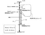
一方、角速度Ωに対するコリオリ力はF=2×m×a sinω0t×Ωであり、駆動振幅aに比例している。このことから、検出回路のLPF出力Vdetectは、Vdetect=kd×a×Ωと表すことができる。A/D変換器316に入力されるLPF310の出力Vdetectは、駆動振幅aに比例しており、これを駆動振幅aに応じた基準電圧(VrefH,VrefL)のA/D変換器316でA/D変換するため、A/D変換後のデータからは駆動振幅aに依存する項を消すことができる。
On the other hand, the Coriolis force with respect to the angular velocity Ω is F = 2 × m × a sin ω0t × Ω, which is proportional to the drive amplitude a. From this, the LPF output Vdetect of the detection circuit can be expressed as Vdetect = kd × a × Ω. The output Vdetect of the
図4は、駆動振動の振幅が異なる状態におけるA/D変換の様子を示す概念図である。A/D変換器316の基準電圧(VrefH,VrefL)が、駆動振幅aと比例していることから、角速度入力Ωに対して、駆動振幅aの如何によらず一定のデジタルコードが出力される。以下、具体的に説明する。 FIG. 4 is a conceptual diagram showing a state of A / D conversion in a state where the amplitudes of drive vibrations are different. Since the reference voltages (VrefH, VrefL) of the A / D converter 316 are proportional to the drive amplitude a, a constant digital code is output with respect to the angular velocity input Ω regardless of the drive amplitude a. . This will be specifically described below.
2つの基準電圧(VrefHおよびVrefL)で規定されるダイナミックレンジをA/D変換器316の変換幅とする。また、駆動振幅が変動する前の状態における検出出力をVdetect1とし、変動後の状態における検出出力をVdetect2とする。このとき、図4に示すように、(VrefH−Vdetect1)に対する(Vdetect1−VrefL)の比は、A1:B1となる。 A dynamic range defined by two reference voltages (VrefH and VrefL) is set as a conversion width of the A / D converter 316. Also, the detection output in the state before the drive amplitude fluctuates is Vdetect1, and the detection output in the state after the fluctuation is Vdetect2. At this time, as shown in FIG. 4, the ratio of (Vdetect1−VrefL) to (VrefH−Vdetect1) is A1: B1.
一方、(VrefH−Vdetect2)に対する(Vdetect2−VrefL)の比は、A2:B2となる。図示されるとおり、A1:B1=A2:B2であり、振幅変動の前後で比の値が変化しない。よって、A/D変換器316から出力されるデジタルコード(256階調であれば、コード0〜コード255のいずれかとなる)は、駆動振幅が変動しても同じであり、物理量の検出感度は一定に保たれる。よって、高精度な検出が可能となる。 On the other hand, the ratio of (Vdetect2-VrefL) to (VrefH-Vdetect2) is A2: B2. As shown in the figure, A1: B1 = A2: B2, and the ratio value does not change before and after the amplitude fluctuation. Therefore, the digital code output from the A / D converter 316 (if it is 256 gradations, any of code 0 to code 255) is the same even if the drive amplitude varies, and the detection sensitivity of the physical quantity is Kept constant. Therefore, highly accurate detection is possible.
図5は、並列型A/D変換器の回路例(2ビット)を示す図である。Rd1〜Rd5はラダー抵抗を構成する。50a〜50dは比較器である。60はエンコーダである。
FIG. 5 is a diagram illustrating a circuit example (2 bits) of the parallel A / D converter. Rd1 to Rd5 constitute a ladder resistor.
以上により、駆動振幅が一定化されていない条件(起動時など)でも、駆動振幅によらず一定の感度のジャイロスコープを構成することができる。しかも、アナログの乗算器を使わず、ADCの基準電圧を利用して感度を一定化しているので温度・トランジスタのパラメータ変動に対して安定である。 As described above, it is possible to configure a gyroscope having a constant sensitivity regardless of the drive amplitude even under a condition where the drive amplitude is not constant (such as when starting up). In addition, since the sensitivity is made constant by using the ADC reference voltage without using an analog multiplier, it is stable against temperature and transistor parameter variations.
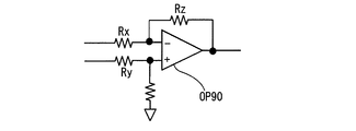
図6は、チャージアンプの回路例を示す図である。検出回路300内に設けられるチャージアンプ302では、信号周波数fsigが、帰還抵抗RF、帰還容量CFで決まる遮断周波数で決まる遮断周波数より高くなる領域で使う。つまり、fsig>1/2πRFCFに設定される。RFは、直流成分の帰還用抵抗であり、大きな抵抗値を使う。図6の回路は、オペアンプOP80と、帰還抵抗RFと、帰還容量CFと、を有する。図7は、差動アンプの回路構成の一例を示す図である。差動アンプ304は、オペアンプOP90を用いて構成することができる。なお、Rx,Ryは入力抵抗であり、Rzは帰還抵抗である。これらはごく一般的な回路であり、動作説明を省く。 FIG. 6 is a diagram illustrating a circuit example of the charge amplifier. The charge amplifier 302 provided in the detection circuit 300 is used in a region where the signal frequency fsig is higher than the cutoff frequency determined by the cutoff frequency determined by the feedback resistor RF and the feedback capacitor CF. That is, fsig> 1 / 2πRFCF is set. RF is a DC component feedback resistor and uses a large resistance value. The circuit in FIG. 6 includes an operational amplifier OP80, a feedback resistor RF, and a feedback capacitor CF. FIG. 7 is a diagram illustrating an example of a circuit configuration of the differential amplifier. The differential amplifier 304 can be configured using an operational amplifier OP90. Rx and Ry are input resistors, and Rz is a feedback resistor. These are very general circuits and will not be described.
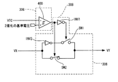
図8は、2値化回路ならびに同期検波回路の回路構成の一例を示す図である。図8では、スイッチミキサによる同期検波回路308を示しているが、ギルバートミキサなど他の構成を使っても良い。また、スイッチミキサを使う場合の2値化回路306としては、図8に示されるようにコンパレータ400でなく、シュミット・トリガ入力のインバータなどを使っても良い。図8の同期検波回路308は、反転経路と正転経路を有し、反転経路にはインバータINV2とスイッチSW1が設けられ、正転経路にはスイッチSW2が設けられる。スイッチSW1は2値化回路306の出力信号によりオン/オフ駆動され、また、スイッチSW2は、インバータINV1の出力信号によってオン/オフ駆動される。
FIG. 8 is a diagram illustrating an example of the circuit configuration of the binarization circuit and the synchronous detection circuit. Although FIG. 8 shows the
なお、A/D変換器316としては、並列型、逐次比較型、パイプライン型、ΔΣ型など、種々の回路構成を採用することができる。 Note that various circuit configurations such as a parallel type, a successive approximation type, a pipeline type, and a ΔΣ type can be employed as the A / D converter 316.
(第2の実施形態)
図9は、本発明の振動型ジャイロスコープの構成の他の例を示す図である。図9の基本的な構成は、図1と同じであるが、AGC回路206における整流動作ならびに積分動作を行う部分の回路構成が異なる。また、検出回路300において、オフセット調整回路320が設けられる点でも図1と異なっている。
(Second Embodiment)
FIG. 9 is a diagram showing another example of the configuration of the vibration gyroscope of the present invention. The basic configuration of FIG. 9 is the same as that of FIG. 1, but the circuit configuration of the
第1の実施形態では、A/D変換器316の基準電圧(リファレンス)を「駆動振幅に対応した電圧」で制御しているが、本実施形態では、A/D変換器316の基準電圧(リファレンス)を「駆動振幅に対応した電圧と、駆動振幅を決定する基準電圧との偏差を増幅した電圧」で制御している。つまり、GCAの制御回路として、駆動振幅検出回路と差動アンプではなく、整流回路と積分回路が一体になった整流・積分回路を採用している。ダイオードD100は半波整流回路を構成している。この回路は、D100に流れる平均電流I1と、D200に流れる電流I2との偏差を積分回路で増幅して出力する回路になっている。I1,I2は抵抗で決定されているので、結局は振幅電圧と基準電圧とを比較していることに他ならない(例えば、発振回路の設計と応用、稲葉保著、CQ出版社参照)。この構成によって、駆動振幅検出回路(図9の場合、整流・積分回路610がこれに相当する)の回路構成を簡素化することができる。よって、回路の占有面積の低減が可能である。 In the first embodiment, the reference voltage (reference) of the A / D converter 316 is controlled by the “voltage corresponding to the drive amplitude”, but in the present embodiment, the reference voltage (reference) of the A / D converter 316 ( Reference) is controlled by “a voltage obtained by amplifying a deviation between a voltage corresponding to the drive amplitude and a reference voltage for determining the drive amplitude”. That is, as a GCA control circuit, a rectification / integration circuit in which a rectification circuit and an integration circuit are integrated is adopted instead of a drive amplitude detection circuit and a differential amplifier. The diode D100 constitutes a half-wave rectifier circuit. This circuit is a circuit that amplifies a deviation between an average current I1 flowing through D100 and a current I2 flowing through D200 by an integrating circuit and outputs the amplified deviation. Since I1 and I2 are determined by resistances, the amplitude voltage and the reference voltage are finally compared (for example, design and application of an oscillation circuit, Yasuo Inaba, see CQ publisher). With this configuration, the circuit configuration of the drive amplitude detection circuit (in the case of FIG. 9, the rectification / integration circuit 610 corresponds to this) can be simplified. Therefore, the area occupied by the circuit can be reduced.
図9において、検出回路のA/D変換器316の基準電圧は、整流・積分回路の出力(つまり、GCAの制御電圧)から取り出されている(図1では、駆動振幅検出回路208の出力からA/D変換器の基準電圧を取り出している)。図9の回路では、発振ループの振幅を示す電圧から、AGCの振幅制御の基準電圧Vref(amptd)に相当する電圧を差し引き、得られた電圧に基づいて、A/D変換器316の基準電圧(VrefH,VrefL)が駆動振幅aと比例するように制御している。 9, the reference voltage of the A / D converter 316 of the detection circuit is extracted from the output of the rectification / integration circuit (that is, the control voltage of the GCA) (in FIG. 1, from the output of the drive amplitude detection circuit 208). The reference voltage of the A / D converter is taken out). In the circuit of FIG. 9, a voltage corresponding to the reference voltage Vref (amptd) for AGC amplitude control is subtracted from the voltage indicating the amplitude of the oscillation loop, and the reference voltage of the A / D converter 316 is calculated based on the obtained voltage. Control is performed so that (VrefH, VrefL) is proportional to the drive amplitude a.
図9において、整流・積分回路(基準振幅との差を算出する回路)610は、抵抗R100,R200と、ダイオードD100,D200と、基準電圧Vref(amptd)を発生する電圧源E1と、オペアンプOP100と、帰還抵抗R300,R400と、帰還容量(積分容量)C100,C200と、により構成される。 In FIG. 9, a rectification / integration circuit (a circuit that calculates a difference from a reference amplitude) 610 includes resistors R100 and R200, diodes D100 and D200, a voltage source E1 that generates a reference voltage Vref (amptd), and an operational amplifier OP100. And feedback resistors R300 and R400 and feedback capacitors (integral capacitors) C100 and C200.
図9において、ノードN1の電圧をVN1とし、ノードN2の電圧をVN2とする。VN1>VN2のとき、電流I1が流れる。また、VN2がVref(amptd)を超えると、電流I2が流れる。オペアンプOP100と、帰還抵抗R300,R400と、帰還容量(積分容量)C100,C200とによって積分回路が構成される。この積分回路は、電流I1と電流I2との差(I1とI2との偏差)を積分し、その差に対応する電圧を生成し、その生成された電圧が、ゲインコントロールアンプ218の制御電圧となる。また、ゲインコントールアンプ218の制御電圧は、検出回路300内の加算器332に供給される。
In FIG. 9, the voltage at the node N1 is VN1, and the voltage at the node N2 is VN2. When VN1> VN2, a current I1 flows. When VN2 exceeds Vref (amptd), a current I2 flows. The operational amplifier OP100, feedback resistors R300 and R400, and feedback capacitors (integral capacitors) C100 and C200 constitute an integration circuit. This integration circuit integrates the difference between I1 and I2 (deviation between I1 and I2), generates a voltage corresponding to the difference, and the generated voltage is the control voltage of
また、検出回路300において、検出信号Vdetectの中心電圧とA/D変換器316の基準電圧の中心電圧が異なる場合においても、オフセット調整回路320を設けることによって、DCオフセットが解消されて矛盾のない処理ができるようになる。図9では、オフセット調整回路320によって生成されるオフセット補償電圧が、加算器332によって、整流・積分回路610の出力信号VQに加算される。これによって、オフセットが補償された、駆動振幅に対応した信号Voffmが生成される。ゲイン調整用の増幅器312は、Voffmの電圧レベル(振幅)を調整する。電圧レベルが調整された信号によって、A/D変換器316の高レベルの基準電圧(VrefH)が、動的に制御される。
Further, in the detection circuit 300, even when the center voltage of the detection signal Vdetect and the center voltage of the reference voltage of the A / D converter 316 are different, by providing the offset
ここでは、電圧レベルが調整された信号そのものがVrefHとして使用される。但し、これに限定されるものではなく、VrefHを発生させる可変基準電圧回路を別途設けて、駆動振動の振幅に対応する電圧信号を制御信号として用いて、その可変基準電圧回路の出力電圧レベルを可変に制御する構成であってもよい。 Here, the signal itself with the adjusted voltage level is used as VrefH. However, the present invention is not limited to this. A variable reference voltage circuit for generating VrefH is separately provided, and a voltage signal corresponding to the amplitude of the drive vibration is used as a control signal, and the output voltage level of the variable reference voltage circuit is set. It may be configured to be variably controlled.
また、図9では、電圧レベルが調整された信号の電圧レベルを、反転増幅器314で反転した信号が、低レベルの基準電圧(VrefL)として使用される。VrefLを発生させる可変基準電圧回路を別途設けて、駆動振動の振幅に対応する信号を反転した信号によって、可変基準電圧回路の出力電圧レベルを可変に制御する構成であってもよい。 In FIG. 9, a signal obtained by inverting the voltage level of the signal whose voltage level has been adjusted by the inverting amplifier 314 is used as the low-level reference voltage (VrefL). A variable reference voltage circuit that generates VrefL may be provided separately, and the output voltage level of the variable reference voltage circuit may be variably controlled by a signal obtained by inverting a signal corresponding to the amplitude of the drive vibration.
すなわち、発振駆動回路(および検出回路)の信号経路の基準バイアス電圧AGND(例えば、AGND=VDD/2)に、オフセット電圧(アンプやトランジスタの特性変動等、種々の要因によって発生する)が重畳されると、そのオフセット電圧は、振動子の駆動振動に対するレシオメトリックを実現する上での誤差の原因となる。そこで、オフセット調整回路320を設けて、オフセット電圧を補償するものである。これによって、駆動振幅検出回路(図9の場合、整流・積分回路610がこれに相当する)の検出出力にオフセットが重畳されている場合でも、検出感度の変動が生じない。本実施形態のジャイロスコープでも、第1の実施形態と同様の効果を得ることができる。
That is, an offset voltage (generated due to various factors such as variations in the characteristics of amplifiers and transistors) is superimposed on the reference bias voltage AGND (for example, AGND = VDD / 2) in the signal path of the oscillation drive circuit (and the detection circuit). Then, the offset voltage causes an error in realizing the ratiometric with respect to the drive vibration of the vibrator. Therefore, an offset
(第3の実施形態)
図10は、本発明の振動型ジャイロスコープの構成のさらに他の例を示す図である。第1の実施形態では、駆動振幅aをAGCで一定に保つ構成を採用している。しかし、本発明を用いると、駆動振幅aによらず、角速度に対する感度を一定にできるため、AGC回路は必須ではなくなる。
(Third embodiment)
FIG. 10 is a diagram showing still another example of the configuration of the vibration gyroscope of the present invention. In the first embodiment, a configuration is adopted in which the drive amplitude a is kept constant at AGC. However, when the present invention is used, the sensitivity to the angular velocity can be made constant regardless of the drive amplitude a, and thus the AGC circuit is not essential.
そこで、本実施形態では、発振駆動回路200における駆動振幅の変動幅を、振幅制限回路500で制限している。その上で、駆動振幅検出回路208の検出信号に基づいて、A/D変換器316の基準電圧(リファレンス)を可変に(適応的に)制御する。なお、振幅制限回路500は、抵抗R100と、ダイオードD10およびD20とを有し、ダイオードD10のアノードには下限電圧V(L)が接続され、ダイオードD20のカソードには、上限電圧V(H)が接続されている。
Therefore, in the present embodiment, the fluctuation range of the drive amplitude in the oscillation drive circuit 200 is limited by the
この場合でも、前掲の実施形態と同様の効果が得られる。また、AGC回路を設けないことによって、回路構成が簡素化され、消費電流が低減され、コストを低下させることができる。 Even in this case, the same effect as the above-described embodiment can be obtained. Further, by not providing the AGC circuit, the circuit configuration is simplified, current consumption is reduced, and cost can be reduced.
図10では、駆動振幅の制限を振幅制限回路500で行っているが、発振駆動回路200内の非線形性により振幅がほぼ一定に保たれる場合には、振幅制限回路500も設ける必要がなくなる。この場合、さらなる回路の簡素化が達成される。また、振幅制限は、振動子100を駆動する増幅器502の出力振幅を制限することによって行ってもよい。
In FIG. 10, the drive amplitude is limited by the
(第4の実施形態) (Fourth embodiment)
本発明のジャイロセンサ(ジャイロスコープ)を、例えば、デジタルカメラの手ぶれ防止に用いた場合、手ぶれ防止機構の発生する振動や、ミラーやシャッターの発生する衝撃に対して影響が少ないことから、より高精度な手ぶれ防止が実現できる。よって、電子機器の性能を向上させることができる。 When the gyro sensor (gyroscope) of the present invention is used, for example, to prevent camera shake of a digital camera, it is less affected by vibration generated by a camera shake prevention mechanism and shock generated by a mirror or shutter. Accurate camera shake prevention can be realized. Therefore, the performance of the electronic device can be improved.
図12は、ジャイロセンサを搭載するカメラ(電子機器)の主要な構成を示すブロック図である。図12のカメラ30は、CPU21と、シャッターボタン22と、変位センサとしてのジャイロセンサ23と、AF(自動焦点ユニット)24と、AE(自動露出ユニット)25と、ドライバ26と、駆動機構27と、CCD(撮像部)28と、シャッター29と、を有する。
FIG. 12 is a block diagram showing a main configuration of a camera (electronic device) equipped with a gyro sensor. 12 includes a
カメラ30は、手ぶれによる撮影画像の乱れを補正するための手振れ補正手段が設けられている。すなわち、CCD28は、駆動機構27によって、例えば、X方向ならびにY方向に独立して移動させることが可能である。駆動機構27は、駆動源として、例えば、アクチュエータ、例えばプランジャ、圧電素子などを備えており、アクチュエータに印加される電圧に応じてCCD28の移動量が変化する。
The
カメラ30に設けられているシャッターボタン22がユーザによって押下されると、シャッター29が動作し、同時に、変位センサとしてのジャイロセンサ23が動作し、かつ、同時に、ドライバ26によって駆動機構27が駆動されて、CCD28の位置を瞬時的に変化させて手振れ補正を行う。
When the
カメラ30には、変位センサとしてのジャイロセンサ23(ジャイロセンサ23を含む物理量測定装置)に同期して動作する可動機構が含まれている。その可動機構は、変位センサとしてのジャイロセンサ23(物理量測定装置)と同時に動作する。すなわち、可動期間の動作期間とジャイロセンサの動作期間とが重なりを有する場合があり得る。
The
ここで、可動機構(可動部)は、例えば機械的な可動部分をもつ構成、あるいは、その位置が変位可能な機械的な構成要素を含む可動部分をもつ構成である。例えば、シャッター29や、アクチュエータ等を含む駆動機構27や、移動可能な構成をもつCCD28が、可動機構(可動部)に該当する。
Here, the movable mechanism (movable portion) has, for example, a configuration having a mechanical movable portion or a configuration having a movable portion including a mechanical component whose position can be displaced. For example, a
よって、変位センサとしてのジャイロセンサ23が動作する場合、可動機構により生じる振動や衝撃の影響を受けて、従来のジャイロセンサならば、その感度が変化する場合もあり得る。すなわち、従来のレシオメトリック構成は、「電源電圧」に対してセンサの感度を一定にしようとする構成であり、電源電圧の変動には対応できるが、上述のような機械的な振動や衝撃に対してはセンサの感度を一定に保つことはできない。
Therefore, when the
しかし、本発明のジャイロセンサ23の場合、「振動子の駆動振幅(駆動振動の振幅)」に対するレシオメトリック構成(すなわち、駆動振動の振幅の変動が生じも検出感度が変化しない新規なレシオメトリック構成)が採用されているため、可動機構からの振動や衝撃の影響を排除できる。よって、カメラ(すなわち電子機器)の撮像性能が向上する。
However, in the case of the
(第5の実施形態)
本実施形態では、本発明のジャイロセンサ(ジャイロスコープ)を、例えば、デジタル一眼レフカメラの手ぶれ防止用に使用する。
(Fifth embodiment)
In the present embodiment, the gyro sensor (gyroscope) of the present invention is used for preventing camera shake of a digital single lens reflex camera, for example.
図13は、本発明のジャイロセンサ(振動型ジャイロスコープ)を内蔵するデジタル一眼レフカメラの主要な構成の一例を示す図である。図13において、図12と共通する部分には同じ参照符号を付している。図13のデジタル一眼レフカメラ31は、図12に示される構成要素に加えて、さらに、AFモータドライバ32と、AFモータ33と、撮像レンズ34と、ミラー跳ね上げ機構36と、ミラー37と、を有する。ミラー跳ね上げ機構36の代わりに、クイックリターン機構を設けることもできる。また、AFモータドライバ32ならびにAFモータ33は、撮影レンズ34の位置を調整してオートフォーカス(自動焦点制御)を実現するためのオートフォーカス(AF)制御機構(AF制御部)を構成する。
FIG. 13 is a diagram illustrating an example of a main configuration of a digital single-lens reflex camera incorporating a gyro sensor (vibrating gyroscope) according to the present invention. In FIG. 13, parts that are the same as those in FIG. 12 are given the same reference numerals. In addition to the components shown in FIG. 12, the digital single
ミラー跳ね上げ機構36は、ミラー37を瞬時的に光軸上から退避させたり、あるいは元の位置に復帰させたりする動作を行うため、その動作に伴って機械的な衝撃が発生する。したがって、可動機構であるミラー跳ね上げ機構36は衝撃源となり得る。また、一眼レフカメラ31に設けられるオートフォーカス(AF)制御機構も、AFモータの駆動や駆動停止に伴って、機械的な衝撃を発生させる場合がある。したがって、可動機構は衝撃源となり得る。
Since the mirror flip-up mechanism 36 performs an operation of momentarily retracting the
デジタル一眼レフカメラ31に搭載される本発明のジャイロセンサ(ジャイロスコープ)23は、衝撃源としての可動機構の動作によって発生する機械的な衝撃に影響されることなく、常に、高精度の角速度等の測定を実行することができる。よって、常に正確な手振れ補正が実現される。
The gyro sensor (gyroscope) 23 of the present invention mounted on the digital single-
(第6の実施形態)
本実施形態では、本発明のジャイロセンサ(ジャイロスコープ)を、例えば、家庭用ゲームコントローラ(携帯型ゲームコントローラ)に搭載する。
(Sixth embodiment)
In this embodiment, the gyro sensor (gyroscope) of the present invention is mounted on, for example, a home game controller (portable game controller).
図14は、本発明のジャイロセンサ(振動型ジャイロスコープ)を内蔵するゲームコントローラの主要な構成の一例を示す図である。ゲームコントローラ40は、ゲーム機本体46と有線通信あるいは無線通信によって接続される。ゲームコントローラ40は、操作スイッチ41と、CPU42と、ジャイロセンサ43と、加速度センサ44と、ゲームコントローラ本体を振動させるためのバイブレータ45と、を有する。CPU42は、ゲーム機本体46に、ゲームを進行させるための制御信号(VQout)等を送信する。また、ゲーム機本体46からCPU42に、バイブレータ45の動作を制御するための指令等(VQin)が入力される。
FIG. 14 is a diagram showing an example of a main configuration of a game controller incorporating a gyro sensor (vibrating gyroscope) according to the present invention. The
バイブレータ45は、臨場感あふれるゲームを楽しむために設けられている。バイブレータ45は、機械的な振動源である。本発明のジャイロセンサ(ジャイロスコープ)43は、例えば、ゲームコントローラ40の姿勢検出のために設けられる。また、加速度センサ44は、例えば、ゲームコントローラ40の傾き検出のために設けられる。
The
本発明のジャイロセンサ(ジャイロスコープ)43は、可動機構であるバイブレータ45の動作(振動)によって発生する機械的な衝撃に影響されることなく、常に、高精度の角速度等の測定を実行することができる。よって、常に、正確な姿勢検出が可能である。
The gyro sensor (gyroscope) 43 of the present invention always performs high-accuracy measurement of angular velocity and the like without being affected by mechanical shocks generated by the operation (vibration) of the
以上説明したように、本発明の幾つかの実施形態によれば、例えば、以下の効果を得ることができる。但し、以下の効果は同時に得られるとは限らず、以下の効果の列挙が、本発明の技術的範囲を不当に制限する根拠として用いられてはならない。
(1)例えば、振動型ジャイロスコープにおいて、駆動振動の振幅を一定に保たなくても角速度に対する感度を一定に保つことができる。
(2)駆動振動の振幅を一定に保つ回路(自動利得制御回路AGC)を持つ場合でも、発振起動時などは駆動振動の振幅は一定でないが、本発明を適用すれば、駆動振動の振幅が一定でなくても、検出感度に対する影響は最小化され、よって、例えば、より安定した感度を持つジャイロスコープを構成できる。
(3)検出感度を一定化する手段として、駆動振動の振幅に応じてA/D変換器の基準電圧(リファレンス)を変化させるという手法を採用しているため、アナログ乗算器やゲインコントロールアンプを使う場合と比較して、温度特性・線形性などの点で優れており、正確な制御を、より簡易に実現することが可能である。
(4)外乱に関係なく物理量の検出感度を一定に保つことができるため、発振起動期間(電源投入時点から発振定常状態に至るまでの期間)においても、有効な、物理量の検出信号を得ることができ、よって、起動の待ち時間を短縮できる。
(5)電源電圧の変動等の電気的な外乱要因に対する対策ならびに機械的な外乱要因(電子機器に加わる衝撃や揺れ等)に対する対策も実現される。よって、電子機器の性能が向上する。
As described above, according to some embodiments of the present invention, for example, the following effects can be obtained. However, the following effects are not always obtained, and the following list of effects should not be used as a basis for unduly limiting the technical scope of the present invention.
(1) For example, in a vibratory gyroscope, sensitivity to angular velocity can be kept constant without keeping the amplitude of drive vibration constant.
(2) Even when a circuit (automatic gain control circuit AGC) that keeps the amplitude of the drive vibration constant is provided, the amplitude of the drive vibration is not constant at the time of oscillation start-up. Even if it is not constant, the influence on the detection sensitivity is minimized. Therefore, for example, a gyroscope having more stable sensitivity can be configured.
(3) Since a method of changing the reference voltage (reference) of the A / D converter according to the amplitude of the drive vibration is adopted as means for making the detection sensitivity constant, an analog multiplier or a gain control amplifier is used. Compared with the case of using, it is superior in terms of temperature characteristics, linearity, etc., and accurate control can be realized more easily.
(4) Since the detection sensitivity of the physical quantity can be kept constant regardless of the disturbance, an effective physical quantity detection signal can be obtained even during the oscillation start-up period (the period from when the power is turned on to the oscillation steady state). Therefore, the waiting time for activation can be shortened.
(5) Countermeasures against electrical disturbance factors such as fluctuations in power supply voltage and mechanical disturbance factors (such as shock and vibration applied to electronic devices) can be realized. Therefore, the performance of the electronic device is improved.
なお、本実施形態について詳述したが、本発明の新規事項および効果から逸脱しない範囲で、多くの変形が可能であることは、当業者には容易に理解できるであろう。したがって、このような変形例は、すべて本発明に含まれるものとする。 In addition, although this embodiment was explained in full detail, it will be easily understood by those skilled in the art that many modifications can be made without departing from the novel matters and effects of the present invention. Therefore, all such modifications are included in the present invention.
例えば、明細書又は図面において、少なくとも一度、より広義または同義な異なる用語と共に記載された用語は、明細書又は図面のいかなる箇所においても、その異なる用語に置き換えることができる。また本実施形態及び変形例の全ての組み合わせも、本発明の範囲に含まれる。また振動子の構造や、検出装置、駆動回路、検出回路、センサ、電子機器の構成及び動作も、本実施形態で説明したものに限定されず、種々の変形実施が可能である。 For example, a term described at least once together with a different term having a broader meaning or the same meaning in the specification or the drawings can be replaced with the different term in any part of the specification or the drawings. All combinations of the present embodiment and the modified examples are also included in the scope of the present invention. Further, the structure of the vibrator and the configurations and operations of the detection device, the drive circuit, the detection circuit, the sensor, and the electronic device are not limited to those described in this embodiment, and various modifications can be made.
上述の実施形態では、物理量トランスデューサが圧電振動子(振動ジャイロ:振動ジャイロスコープ素子)であり、センサがジャイロセンサである場合を例にとり説明したが、本発明はこれに限定されるものではない。本発明は、例えば、振動型ジャイロスコープの駆動・検出回路全般に適用可能である。水晶などの圧電駆動型の物理量トランスデューサだけでなく、シリコンMEMSのような静電駆動型でも同様の構成が可能であり、同様の効果が得られる。 In the above-described embodiment, the case where the physical quantity transducer is a piezoelectric vibrator (vibration gyro: vibration gyroscope element) and the sensor is a gyro sensor has been described as an example. However, the present invention is not limited to this. The present invention can be applied to, for example, a general drive / detection circuit of a vibration gyroscope. The same configuration is possible not only with a piezoelectric drive type physical quantity transducer such as quartz but also with an electrostatic drive type such as silicon MEMS, and the same effect can be obtained.
また、本発明の物理量測定装置は、例えば、ビデオカメラやデジタルカメラ、カーナビゲーションシステム、航空機やロボットに搭載することができる。上述のとおり、本発明の物理量測定装置は、外乱に関係なく物理量の検出感度を一定に保つことができるため、発振起動期間(電源投入時点から発振定常状態に至るまでの期間)においても、有効な物理量の検出信号を得ることができ、よって、起動の待ち時間を短縮できる。 The physical quantity measuring device of the present invention can be mounted on, for example, a video camera, a digital camera, a car navigation system, an aircraft, or a robot. As described above, the physical quantity measuring device according to the present invention can maintain the detection sensitivity of the physical quantity regardless of the disturbance, so that it is effective even during the oscillation start-up period (period from when the power is turned on until the oscillation steady state). Therefore, it is possible to obtain a detection signal with a large physical quantity, and therefore, the waiting time for activation can be shortened.
また、電源電圧の変動等の電気的な外乱要因に対する対策ならびに機械的な外乱要因(電子機器に加わる衝撃や揺れ等)に対する対策も実現される。特に、本発明のジャイロセンサを、ジャイロセンサと同時に動作する可動機構を持つ電子機器に用いた場合、可動機構の発生する振動の影響によるセンサの精度低下を防ぐことができる。例えば、本発明のジャイロセンサをデジタルカメラの手ぶれ防止に用いた場合、手ぶれ防止機構の発生する振動や、ミラーやシャッターの発生する衝撃に対して影響が少ないことから、より高精度な手ぶれ防止が実現できる。このように、電子機器の性能を向上させることができる。 In addition, measures against electrical disturbance factors such as fluctuations in the power supply voltage and measures against mechanical disturbance factors (such as impact and vibration applied to the electronic device) can be realized. In particular, when the gyro sensor of the present invention is used in an electronic device having a movable mechanism that operates simultaneously with the gyro sensor, it is possible to prevent a decrease in accuracy of the sensor due to the influence of vibration generated by the movable mechanism. For example, when the gyro sensor of the present invention is used to prevent camera shake of a digital camera, it has less influence on vibrations generated by the camera shake prevention mechanism and shocks generated by mirrors and shutters. realizable. Thus, the performance of the electronic device can be improved.
100 振動子(振動型ジャイロスコープ素子)、200 発振駆動回路(発振回路)、206 AGC回路、208 駆動振幅検出回路、210 整流回路、
212 平滑回路、214 基準電圧回路(バンドギャップ回路)、
216 差動増幅器、218 ゲインコントロールアンプ(GCA)、
300 検出回路、302 チャージアンプ(Q/V変換回路)、
304 差動増幅回路、306 2値化回路 308 同期検波回路、
310 ローパスフィルタ(LPF)、
312 ゲイン調整用増幅器(基準電圧生成のために電圧振幅を調整するための回路)、314 反転増幅器
100 vibrator (vibration gyroscope element), 200 oscillation drive circuit (oscillation circuit), 206 AGC circuit, 208 drive amplitude detection circuit, 210 rectifier circuit,
212 smoothing circuit, 214 reference voltage circuit (band gap circuit),
216 differential amplifier, 218 gain control amplifier (GCA),
300 detection circuit, 302 charge amplifier (Q / V conversion circuit),
304 differential amplifier circuit, 306
310 Low-pass filter (LPF),
312 Gain adjustment amplifier (circuit for adjusting voltage amplitude for generating reference voltage), 314 Inverting amplifier
Claims (11)
前記物理量トランスデューサから出力されるアナログの検出信号を検波回路によって検波した後、検波された信号を、A/D変換器によってデジタル信号に変換して出力する検出回路と、を含み、
前記発振駆動回路は、前記駆動振動の振幅を検出する駆動振幅検出回路を有し、
前記検出回路に含まれる前記A/D変換器の基準電圧の電圧レベルは、前記駆動振幅検出回路の検出出力信号に基づいて、前記A/D変換器の変換幅が、前記駆動振動の振幅に比例するように制御されることを特徴とする物理量測定装置。 An oscillation drive circuit that forms an oscillation loop with the physical quantity transducer, and that excites drive vibration in the physical quantity transducer;
A detection circuit that detects an analog detection signal output from the physical quantity transducer by a detection circuit, converts the detected signal into a digital signal by an A / D converter, and outputs the digital signal.
The oscillation drive circuit has a drive amplitude detection circuit for detecting the amplitude of the drive vibration,
The voltage level of the reference voltage of the A / D converter included in the detection circuit is determined based on the detection output signal of the drive amplitude detection circuit so that the conversion width of the A / D converter becomes the amplitude of the drive vibration. A physical quantity measuring device controlled to be proportional .
前記発振駆動回路は、前記駆動振動の振幅を一定にするためのAGC回路を有し、前記駆動振幅検出回路は、前記AGC回路を構成する回路の一つであることを特徴とする物理量測定装置。 The physical quantity measuring device according to claim 1 ,
The oscillation drive circuit has an AGC circuit for making the amplitude of the drive vibration constant, and the drive amplitude detection circuit is one of the circuits constituting the AGC circuit. .
前記駆動振幅検出回路の検出出力信号および前記検出出力信号の電圧レベルを反転した信号の少なくとも一方が、前記A/D変換器の前記基準電圧として使用されることを特徴とする物理量測定装置。 The physical quantity measuring device according to claim 1 or 2 ,
At least one of a detection output signal of the drive amplitude detection circuit and a signal obtained by inverting the voltage level of the detection output signal is used as the reference voltage of the A / D converter.
前記駆動振幅検出回路の検出出力信号の電圧レベルを調整することによって得られる信号を第1の信号とし、前記第1の信号の電圧レベルを反転した信号を第2の信号とした場合、前記第1の信号および前記第2の信号の少なくとも一方が、前記A/D変換器の前記基準電圧として使用されることを特徴とする物理量測定装置。 The physical quantity measuring device according to claim 1 or 2 ,
When the signal obtained by adjusting the voltage level of the detection output signal of the drive amplitude detection circuit is the first signal and the signal obtained by inverting the voltage level of the first signal is the second signal, At least one of the first signal and the second signal is used as the reference voltage of the A / D converter.
前記検出回路は、前記駆動振幅検出回路の検出出力信号に重畳されるオフセット電圧を補償するためのオフセット調整回路を有することを特徴とする物理量測定装置。 The physical quantity measuring device according to claim 3 or 4 , wherein
The physical quantity measuring device, wherein the detection circuit includes an offset adjustment circuit for compensating an offset voltage superimposed on a detection output signal of the drive amplitude detection circuit.
前記駆動振幅検出回路は、
前記発振ループの発振信号を整流する整流回路と、
前記整流回路の出力信号を平滑する平滑回路と、
を有することを特徴とする物理量測定装置。 The physical quantity measuring device according to any one of claims 1 to 5 ,
The drive amplitude detection circuit includes:
A rectifier circuit for rectifying an oscillation signal of the oscillation loop;
A smoothing circuit for smoothing the output signal of the rectifier circuit;
A physical quantity measuring device comprising:
前記駆動振幅検出回路は、
前記発振ループの発振信号を整流する整流回路と、整流した信号を積分する積分回路とが一体化された整流・積分回路により構成されることを特徴とする物理量測定装置。 The physical quantity measuring device according to any one of claims 1 to 5 ,
The drive amplitude detection circuit includes:
A physical quantity measuring device comprising a rectification / integration circuit in which a rectification circuit for rectifying an oscillation signal of the oscillation loop and an integration circuit for integrating the rectified signal are integrated.
前記発振駆動回路は、前記駆動振動の振幅の上限および下限の少なくとも一方を規制するための振幅制限回路を有することを特徴とする物理量測定装置。 The physical quantity measuring device according to claim 1 ,
The physical quantity measuring device, wherein the oscillation driving circuit includes an amplitude limiting circuit for regulating at least one of an upper limit and a lower limit of the amplitude of the driving vibration.
前記物理量測定装置はジャイロセンサであり、
前記物理量トランスデューサは、前記発振駆動回路によって駆動振動が励振されると共に、角速度に応じた振幅の検出信号を生成する振動型ジャイロスコープ素子であることを特徴とする物理量測定装置。 The physical quantity measuring device according to any one of claims 1 to 8 ,
The physical quantity measuring device is a gyro sensor,
The physical quantity measuring device is a vibration type gyroscope element that generates a detection signal having an amplitude corresponding to an angular velocity while driving vibration is excited by the oscillation drive circuit.
可動機構と、
を含むことを特徴とする電子機器。 The physical quantity measuring device according to any one of claims 1 to 9 ,
A movable mechanism;
An electronic device comprising:
前記物理量測定装置の動作期間と前記可動機構の動作期間が重なりを有することを特徴とする電子機器。 The electronic device according to claim 10 ,
An electronic apparatus, wherein an operation period of the physical quantity measuring device and an operation period of the movable mechanism overlap each other.
Priority Applications (3)
| Application Number | Priority Date | Filing Date | Title |
|---|---|---|---|
| JP2008307619A JP5365173B2 (en) | 2008-02-29 | 2008-12-02 | Physical quantity measuring device and electronic device |
| CN2009101185396A CN101520327B (en) | 2008-02-29 | 2009-02-26 | Physical quantity measuring apparatus and electronic device |
| US12/395,359 US8186218B2 (en) | 2008-02-29 | 2009-02-27 | Physical quantity measuring apparatus and electronic device |
Applications Claiming Priority (3)
| Application Number | Priority Date | Filing Date | Title |
|---|---|---|---|
| JP2008049286 | 2008-02-29 | ||
| JP2008049286 | 2008-02-29 | ||
| JP2008307619A JP5365173B2 (en) | 2008-02-29 | 2008-12-02 | Physical quantity measuring device and electronic device |
Publications (3)
| Publication Number | Publication Date |
|---|---|
| JP2009229447A JP2009229447A (en) | 2009-10-08 |
| JP2009229447A5 JP2009229447A5 (en) | 2012-01-19 |
| JP5365173B2 true JP5365173B2 (en) | 2013-12-11 |
Family
ID=41012165
Family Applications (1)
| Application Number | Title | Priority Date | Filing Date |
|---|---|---|---|
| JP2008307619A Expired - Fee Related JP5365173B2 (en) | 2008-02-29 | 2008-12-02 | Physical quantity measuring device and electronic device |
Country Status (3)
| Country | Link |
|---|---|
| US (1) | US8186218B2 (en) |
| JP (1) | JP5365173B2 (en) |
| CN (1) | CN101520327B (en) |
Families Citing this family (67)
| Publication number | Priority date | Publication date | Assignee | Title |
|---|---|---|---|---|
| JP2009244019A (en) * | 2008-03-31 | 2009-10-22 | Seiko Npc Corp | Angular velocity detection apparatus |
| JP2010169532A (en) * | 2009-01-22 | 2010-08-05 | Panasonic Corp | Drive circuit and physical quantity sensor apparatus |
| US8714012B2 (en) * | 2010-02-16 | 2014-05-06 | Stmicroelectronics S.R.L. | Microelectromechanical gyroscope with inversion of actuation forces, and method for actuating a microelectromechanical gyroscope |
| JP5362097B2 (en) * | 2010-02-17 | 2013-12-11 | 株式会社村田製作所 | Vibration type inertial force sensor |
| JP5717376B2 (en) * | 2010-03-31 | 2015-05-13 | シチズンホールディングス株式会社 | Physical quantity sensor |
| JP2011226941A (en) * | 2010-04-21 | 2011-11-10 | Seiko Epson Corp | Vibration-type force detection sensor and vibration-type force detector |
| US8378756B2 (en) * | 2010-05-18 | 2013-02-19 | Taiwan Semiconductor Manufacturing Company, Ltd. | Drive loop for MEMS oscillator |
| JP5569245B2 (en) * | 2010-08-17 | 2014-08-13 | セイコーエプソン株式会社 | Integrated circuit device and electronic apparatus |
| CN103221779B (en) | 2010-09-18 | 2017-05-31 | 快捷半导体公司 | The axle inertial sensor of micromechanics monoblock type six |
| EP2616388A4 (en) | 2010-09-18 | 2014-08-13 | Fairchild Semiconductor | Sealed packaging for microelectromechanical systems |
| US8813564B2 (en) | 2010-09-18 | 2014-08-26 | Fairchild Semiconductor Corporation | MEMS multi-axis gyroscope with central suspension and gimbal structure |
| US9352961B2 (en) | 2010-09-18 | 2016-05-31 | Fairchild Semiconductor Corporation | Flexure bearing to reduce quadrature for resonating micromachined devices |
| EP2616772B1 (en) | 2010-09-18 | 2016-06-22 | Fairchild Semiconductor Corporation | Micromachined monolithic 3-axis gyroscope with single drive |
| CN103221795B (en) | 2010-09-20 | 2015-03-11 | 快捷半导体公司 | Microelectromechanical pressure sensor including reference capacitor |
| JP5975601B2 (en) | 2011-02-25 | 2016-08-23 | セイコーエプソン株式会社 | Detection circuit, physical quantity detection device, angular velocity detection device, integrated circuit device, and electronic apparatus |
| JP5638419B2 (en) * | 2011-02-25 | 2014-12-10 | セイコーエプソン株式会社 | Signal processing circuit, physical quantity detection device, angular velocity detection device, integrated circuit device, and electronic apparatus |
| JP5559733B2 (en) * | 2011-03-31 | 2014-07-23 | シチズンホールディングス株式会社 | Physical quantity sensor |
| JP2012227762A (en) * | 2011-04-20 | 2012-11-15 | Seiko Epson Corp | Oscillation circuit |
| JP5561237B2 (en) * | 2011-04-27 | 2014-07-30 | 株式会社デンソー | Vibrator drive circuit |
| US9091539B2 (en) * | 2011-06-10 | 2015-07-28 | Honeywell International Inc. | Gyroscope dynamic motor amplitude compensation for enhanced rate estimation during startup |
| LU91839B1 (en) * | 2011-07-08 | 2013-01-09 | Iee Sarl | Impedance measurement system |
| US9488693B2 (en) | 2012-04-04 | 2016-11-08 | Fairchild Semiconductor Corporation | Self test of MEMS accelerometer with ASICS integrated capacitors |
| EP2648334B1 (en) | 2012-04-05 | 2020-06-10 | Fairchild Semiconductor Corporation | Mems device front-end charge amplifier |
| EP2647952B1 (en) | 2012-04-05 | 2017-11-15 | Fairchild Semiconductor Corporation | Mems device automatic-gain control loop for mechanical amplitude drive |
| EP2647955B8 (en) | 2012-04-05 | 2018-12-19 | Fairchild Semiconductor Corporation | MEMS device quadrature phase shift cancellation |
| US9625272B2 (en) | 2012-04-12 | 2017-04-18 | Fairchild Semiconductor Corporation | MEMS quadrature cancellation and signal demodulation |
| KR101354782B1 (en) * | 2012-05-25 | 2014-01-22 | 삼성전기주식회사 | Detecting appartus for gyro sensor signal and method thereof |
| DE102013014881B4 (en) | 2012-09-12 | 2023-05-04 | Fairchild Semiconductor Corporation | Enhanced silicon via with multi-material fill |
| ITTO20121116A1 (en) * | 2012-12-20 | 2014-06-21 | St Microelectronics Srl | CIRCUIT AND DYNAMIC COMPENSATION METHOD OF OFFSET FOR A MEMS SENSOR DEVICE |
| US9109901B2 (en) * | 2013-03-08 | 2015-08-18 | Freescale Semiconductor Inc. | System and method for monitoring a gyroscope |
| US9459274B2 (en) | 2013-03-13 | 2016-10-04 | Invensense, Inc. | Round-robin sensing device and method of use |
| US9759564B2 (en) | 2013-03-15 | 2017-09-12 | Fairchild Semiconductor Corporation | Temperature and power supply calibration |
| JP6197323B2 (en) * | 2013-03-22 | 2017-09-20 | セイコーエプソン株式会社 | Detection device, sensor, gyro sensor, electronic device, and moving object |
| JP6222423B2 (en) * | 2013-03-28 | 2017-11-01 | セイコーエプソン株式会社 | Physical quantity sensor, electronic device and moving object |
| JP6222425B2 (en) | 2013-04-24 | 2017-11-01 | セイコーエプソン株式会社 | Physical quantity detection circuit, physical quantity detection device, electronic device, and moving object |
| JP6197347B2 (en) | 2013-04-24 | 2017-09-20 | セイコーエプソン株式会社 | Electronic equipment and physical quantity detection device |
| JP6222426B2 (en) | 2013-04-24 | 2017-11-01 | セイコーエプソン株式会社 | Physical quantity detection circuit, physical quantity detection device, electronic device, and moving object |
| US9109894B2 (en) * | 2013-04-26 | 2015-08-18 | Maxim Integrated Products, Inc. | Gyroscope shock and disturbance detection circuit |
| KR20150015932A (en) * | 2013-08-02 | 2015-02-11 | 삼성전기주식회사 | Apparatus and Method for driving gyro sensor |
| US9332369B2 (en) * | 2013-10-22 | 2016-05-03 | Infineon Technologies Ag | System and method for automatic calibration of a transducer |
| JP6213165B2 (en) * | 2013-11-07 | 2017-10-18 | セイコーエプソン株式会社 | Detection device, sensor, electronic device, and moving object |
| JP6303411B2 (en) * | 2013-11-07 | 2018-04-04 | セイコーエプソン株式会社 | Detection device, sensor, electronic device, and moving object |
| JP6307840B2 (en) * | 2013-11-07 | 2018-04-11 | セイコーエプソン株式会社 | Detection device, sensor, electronic device, and moving object |
| JP6206113B2 (en) * | 2013-11-20 | 2017-10-04 | 株式会社村田製作所 | Vibrator drive circuit |
| JP6287151B2 (en) * | 2013-12-11 | 2018-03-07 | セイコーエプソン株式会社 | Detection device, sensor, electronic device, and moving object |
| JP6187305B2 (en) * | 2014-02-18 | 2017-08-30 | 株式会社デンソー | Gyro sensor |
| CN104848847B (en) * | 2014-02-19 | 2017-11-03 | 无锡华润上华科技有限公司 | A kind of gyro sensor control circuit and electronic installation |
| CN103791897B (en) * | 2014-02-20 | 2016-05-11 | 北京华力创通科技股份有限公司 | Impel the circuit of micromechanical gyro fast start-up |
| US10036652B2 (en) * | 2014-02-24 | 2018-07-31 | The Regents Of The University Of California | Utilization of mechanical quadrature in silicon MEMS vibratory gyroscope to increase and expand the long term in-run bias stability |
| US9835647B2 (en) | 2014-03-18 | 2017-12-05 | Fairchild Semiconductor Corporation | Apparatus and method for extending analog front end sense range of a high-Q MEMS sensor |
| TWI576679B (en) * | 2014-06-11 | 2017-04-01 | 宇能電科技股份有限公司 | Offset voltage automatic compensation system |
| JP5811239B2 (en) * | 2014-06-25 | 2015-11-11 | セイコーエプソン株式会社 | Integrated circuit device and electronic apparatus |
| DE102014010056B4 (en) * | 2014-07-07 | 2016-02-25 | Northrop Grumman Litef Gmbh | A control device and method for minimizing scale factor errors of a rotation rate sensor |
| JP2016171493A (en) * | 2015-03-13 | 2016-09-23 | セイコーエプソン株式会社 | Circuit device, electronic apparatus and moving body |
| US10458839B1 (en) | 2015-11-04 | 2019-10-29 | General Electric Company | Methods and systems for monitoring a dynamic system |
| CN105403220A (en) * | 2015-12-22 | 2016-03-16 | 无锡信大气象传感网科技有限公司 | Carrier based system for detecting trajectory of motion |
| CN105466427A (en) * | 2015-12-22 | 2016-04-06 | 无锡信大气象传感网科技有限公司 | Carrier movement track detection system based on amplifying and filtering circuit |
| CN105651282A (en) * | 2015-12-22 | 2016-06-08 | 无锡信大气象传感网科技有限公司 | Radio frequency identification based system for detecting trajectory of motion of carrier |
| JP6705283B2 (en) * | 2016-05-20 | 2020-06-03 | 株式会社デンソー | Gyro sensor device |
| JP6571064B2 (en) * | 2016-11-21 | 2019-09-04 | 株式会社東芝 | Detection device and sensor device |
| CN107036589B (en) * | 2017-04-20 | 2018-02-23 | 中国人民解放军国防科学技术大学 | A kind of angle measurement system and its method for MEMS gyroscope |
| IT201700103058A1 (en) * | 2017-09-14 | 2019-03-14 | St Microelectronics Srl | CIRCUIT AND DRIVING METHOD FOR A MEMS GYROSCOPE AND ITS MEMS GYROSCOPE |
| CN108332733B (en) * | 2018-01-26 | 2020-05-19 | 珠海全志科技股份有限公司 | Driving and detecting device of micro-mechanical single-vibrator three-axis gyroscope |
| CN108332732B (en) * | 2018-01-26 | 2020-05-19 | 珠海全志科技股份有限公司 | Driving and detecting device of micro-mechanical single-vibrator three-axis gyroscope |
| JP2021071382A (en) * | 2019-10-31 | 2021-05-06 | セイコーエプソン株式会社 | Physical quantity sensor, electronic apparatus, and mobile body |
| CN110946572B (en) * | 2019-12-18 | 2022-04-15 | 郑州轻工业大学 | Wireless Electrocardiogram (ECG) acquisition monitoring device |
| CN112146638B (en) * | 2020-09-11 | 2022-10-28 | 中国船舶重工集团公司第七0七研究所 | Resonant gyroscope amplitude-stabilized excitation effective value detection circuit and method thereof |
Family Cites Families (19)
| Publication number | Priority date | Publication date | Assignee | Title |
|---|---|---|---|---|
| JPS61258110A (en) * | 1985-05-13 | 1986-11-15 | Hitachi Ltd | Angular velocity sensor |
| JPH06194178A (en) * | 1992-10-12 | 1994-07-15 | Nippon Soken Inc | Angular velocity sensor |
| JPH0736613A (en) * | 1993-07-07 | 1995-02-07 | Tokin Corp | Data input device |
| JPH0875473A (en) * | 1994-09-08 | 1996-03-22 | Nissan Motor Co Ltd | Vibration gyro device |
| JPH1144540A (en) * | 1997-07-25 | 1999-02-16 | Denso Corp | Vibration-type angular velocity sensor |
| US6508122B1 (en) * | 1999-09-16 | 2003-01-21 | American Gnc Corporation | Microelectromechanical system for measuring angular rate |
| JP3520821B2 (en) * | 1999-10-29 | 2004-04-19 | 株式会社村田製作所 | Self-diagnosis circuit for vibration gyro |
| WO2001069266A1 (en) * | 2000-03-13 | 2001-09-20 | Microsensors, Inc. | Method of driving mems sensor with balanced four-phase comb drive |
| JP4668407B2 (en) | 2000-12-08 | 2011-04-13 | 京セラキンセキ株式会社 | Angular velocity sensor |
| US6564636B2 (en) * | 2001-08-22 | 2003-05-20 | Honeywell International Inc. | Wide band digital phase locked loop (PLL) with a half-frequency output |
| JP2004053396A (en) * | 2002-07-19 | 2004-02-19 | Matsushita Electric Ind Co Ltd | Angular velocity sensor and car using it |
| JP2005241625A (en) * | 2004-01-27 | 2005-09-08 | Seiko Epson Corp | Clock-generating device, vibration type gyro sensor, navigation device, imaging apparatus, and electronic device |
| JP4411529B2 (en) * | 2004-08-05 | 2010-02-10 | 株式会社デンソー | Vibration type angular velocity sensor |
| JP4258466B2 (en) * | 2004-12-16 | 2009-04-30 | セイコーエプソン株式会社 | Piezoelectric gyro element and piezoelectric gyroscope |
| JP2008089577A (en) * | 2006-09-08 | 2008-04-17 | Seiko Epson Corp | Drive unit, physical quantity measuring apparatus, and electronic apparatus |
| JP4449972B2 (en) * | 2006-11-10 | 2010-04-14 | セイコーエプソン株式会社 | Detection device, sensor and electronic device |
| JP4211840B2 (en) * | 2006-11-10 | 2009-01-21 | セイコーエプソン株式会社 | Detection device, sensor and electronic device |
| US7779688B2 (en) * | 2006-12-20 | 2010-08-24 | Epson Toyocom Corporation | Vibration gyro sensor |
| JP2008209182A (en) | 2007-02-26 | 2008-09-11 | Seiko Epson Corp | Detection apparatus, sensor, and electronic apparatus |
-
2008
- 2008-12-02 JP JP2008307619A patent/JP5365173B2/en not_active Expired - Fee Related
-
2009
- 2009-02-26 CN CN2009101185396A patent/CN101520327B/en not_active Expired - Fee Related
- 2009-02-27 US US12/395,359 patent/US8186218B2/en active Active
Also Published As
| Publication number | Publication date |
|---|---|
| JP2009229447A (en) | 2009-10-08 |
| CN101520327A (en) | 2009-09-02 |
| CN101520327B (en) | 2012-04-04 |
| US20090217757A1 (en) | 2009-09-03 |
| US8186218B2 (en) | 2012-05-29 |
Similar Documents
| Publication | Publication Date | Title |
|---|---|---|
| JP5365173B2 (en) | Physical quantity measuring device and electronic device | |
| US7069783B2 (en) | Angular velocity sensor | |
| JP4534741B2 (en) | Gyro sensor | |
| JP5360361B2 (en) | Angular velocity detector circuit, angular velocity detector, and failure determination system | |
| JP4310571B2 (en) | Capacitance detection type vibration gyro and capacitance change detection method | |
| JP6641712B2 (en) | Circuit device, electronic equipment and moving object | |
| US7849746B2 (en) | Driver device, physical quantity measuring device, and electronic instrument | |
| US8325243B2 (en) | Image stabilization control circuit for correcting vibration-caused displacement of optical axis, and image pickup apparatus provided with the same | |
| JP2009200888A (en) | Mems oscillator | |
| JP2008286597A (en) | Detection device, detection method and electronic device | |
| JP4779692B2 (en) | Oscillation circuit and physical quantity transducer | |
| JP4867385B2 (en) | Oscillation circuit and physical quantity transducer | |
| US8026949B2 (en) | Image stabilization control circuit for correcting vibration-caused displacement of optical axis, and image pickup apparatus provided with the same | |
| US7692506B2 (en) | Oscillation driver device, physical quantity measuring device, and electronic instrument | |
| JP2001116553A (en) | Vibration drive voltage automatic gain control circuit of microgyroscope | |
| JP2009168588A (en) | Detection circuit, physical quantity measuring device, gyro sensor, and electronic device | |
| JP2001099658A (en) | Circuit for compensating for angular velocity output of micro gyroscope | |
| JP5040117B2 (en) | Oscillation circuit, physical quantity transducer, and vibration gyro sensor | |
| JP2005127978A (en) | Oscillating circuit and angular velocity sensor | |
| JP2004212111A (en) | Angular velocity sensor | |
| JP2006105659A (en) | Piezoelectric vibration gyro, and sensitivity regulation method therefor | |
| JP2009244019A (en) | Angular velocity detection apparatus | |
| JP2006153715A (en) | Vibration gyroscope | |
| JP5622001B2 (en) | CIRCUIT FOR ANGLE Velocity Detection Device, Angle Detection Device, and Failure Determination System | |
| JP2010237137A (en) | Angular velocity sensor |
Legal Events
| Date | Code | Title | Description |
|---|---|---|---|
| A521 | Written amendment |
Free format text: JAPANESE INTERMEDIATE CODE: A523 Effective date: 20111129 |
|
| A621 | Written request for application examination |
Free format text: JAPANESE INTERMEDIATE CODE: A621 Effective date: 20111129 |
|
| A977 | Report on retrieval |
Free format text: JAPANESE INTERMEDIATE CODE: A971007 Effective date: 20121017 |
|
| A131 | Notification of reasons for refusal |
Free format text: JAPANESE INTERMEDIATE CODE: A131 Effective date: 20121023 |
|
| A521 | Written amendment |
Free format text: JAPANESE INTERMEDIATE CODE: A523 Effective date: 20121220 |
|
| TRDD | Decision of grant or rejection written | ||
| A01 | Written decision to grant a patent or to grant a registration (utility model) |
Free format text: JAPANESE INTERMEDIATE CODE: A01 Effective date: 20130813 |
|
| A61 | First payment of annual fees (during grant procedure) |
Free format text: JAPANESE INTERMEDIATE CODE: A61 Effective date: 20130826 |
|
| R150 | Certificate of patent or registration of utility model |
Free format text: JAPANESE INTERMEDIATE CODE: R150 |
|
| S531 | Written request for registration of change of domicile |
Free format text: JAPANESE INTERMEDIATE CODE: R313531 |
|
| R350 | Written notification of registration of transfer |
Free format text: JAPANESE INTERMEDIATE CODE: R350 |
|
| LAPS | Cancellation because of no payment of annual fees |