JP5357063B2 - 画像センサ - Google Patents
画像センサ Download PDFInfo
- Publication number
- JP5357063B2 JP5357063B2 JP2009553578A JP2009553578A JP5357063B2 JP 5357063 B2 JP5357063 B2 JP 5357063B2 JP 2009553578 A JP2009553578 A JP 2009553578A JP 2009553578 A JP2009553578 A JP 2009553578A JP 5357063 B2 JP5357063 B2 JP 5357063B2
- Authority
- JP
- Japan
- Prior art keywords
- charge
- node
- pixel
- gate
- transistor
- Prior art date
- Legal status (The legal status is an assumption and is not a legal conclusion. Google has not performed a legal analysis and makes no representation as to the accuracy of the status listed.)
- Active
Links
- 238000006243 chemical reaction Methods 0.000 claims description 19
- 230000004044 response Effects 0.000 claims description 5
- 239000000758 substrate Substances 0.000 claims description 5
- 238000003384 imaging method Methods 0.000 claims 1
- 238000009792 diffusion process Methods 0.000 description 24
- XUIMIQQOPSSXEZ-UHFFFAOYSA-N Silicon Chemical compound [Si] XUIMIQQOPSSXEZ-UHFFFAOYSA-N 0.000 description 4
- 230000000875 corresponding effect Effects 0.000 description 4
- 229910052710 silicon Inorganic materials 0.000 description 4
- 239000010703 silicon Substances 0.000 description 4
- 238000010586 diagram Methods 0.000 description 3
- 238000000034 method Methods 0.000 description 3
- 230000008569 process Effects 0.000 description 3
- 238000005070 sampling Methods 0.000 description 3
- 230000003213 activating effect Effects 0.000 description 2
- 230000002596 correlated effect Effects 0.000 description 2
- 230000007547 defect Effects 0.000 description 2
- 239000002019 doping agent Substances 0.000 description 2
- 230000000694 effects Effects 0.000 description 2
- 239000002184 metal Substances 0.000 description 2
- 230000003287 optical effect Effects 0.000 description 2
- 206010034972 Photosensitivity reaction Diseases 0.000 description 1
- 230000009286 beneficial effect Effects 0.000 description 1
- 230000008859 change Effects 0.000 description 1
- 230000000295 complement effect Effects 0.000 description 1
- 238000002955 isolation Methods 0.000 description 1
- 230000036211 photosensitivity Effects 0.000 description 1
- 229910021420 polycrystalline silicon Inorganic materials 0.000 description 1
- 229920005591 polysilicon Polymers 0.000 description 1
- 238000005549 size reduction Methods 0.000 description 1
Images


Classifications
-
- H—ELECTRICITY
- H01—ELECTRIC ELEMENTS
- H01L—SEMICONDUCTOR DEVICES NOT COVERED BY CLASS H10
- H01L27/00—Devices consisting of a plurality of semiconductor or other solid-state components formed in or on a common substrate
- H01L27/14—Devices consisting of a plurality of semiconductor or other solid-state components formed in or on a common substrate including semiconductor components sensitive to infrared radiation, light, electromagnetic radiation of shorter wavelength or corpuscular radiation and specially adapted either for the conversion of the energy of such radiation into electrical energy or for the control of electrical energy by such radiation
- H01L27/144—Devices controlled by radiation
- H01L27/146—Imager structures
- H01L27/14601—Structural or functional details thereof
- H01L27/14603—Special geometry or disposition of pixel-elements, address-lines or gate-electrodes
-
- H—ELECTRICITY
- H04—ELECTRIC COMMUNICATION TECHNIQUE
- H04N—PICTORIAL COMMUNICATION, e.g. TELEVISION
- H04N25/00—Circuitry of solid-state image sensors [SSIS]; Control thereof
- H04N25/70—SSIS architectures; Circuits associated therewith
- H04N25/76—Addressed sensors, e.g. MOS or CMOS sensors
-
- H—ELECTRICITY
- H01—ELECTRIC ELEMENTS
- H01L—SEMICONDUCTOR DEVICES NOT COVERED BY CLASS H10
- H01L27/00—Devices consisting of a plurality of semiconductor or other solid-state components formed in or on a common substrate
- H01L27/14—Devices consisting of a plurality of semiconductor or other solid-state components formed in or on a common substrate including semiconductor components sensitive to infrared radiation, light, electromagnetic radiation of shorter wavelength or corpuscular radiation and specially adapted either for the conversion of the energy of such radiation into electrical energy or for the control of electrical energy by such radiation
- H01L27/144—Devices controlled by radiation
- H01L27/146—Imager structures
- H01L27/14601—Structural or functional details thereof
- H01L27/14609—Pixel-elements with integrated switching, control, storage or amplification elements
-
- H—ELECTRICITY
- H01—ELECTRIC ELEMENTS
- H01L—SEMICONDUCTOR DEVICES NOT COVERED BY CLASS H10
- H01L27/00—Devices consisting of a plurality of semiconductor or other solid-state components formed in or on a common substrate
- H01L27/14—Devices consisting of a plurality of semiconductor or other solid-state components formed in or on a common substrate including semiconductor components sensitive to infrared radiation, light, electromagnetic radiation of shorter wavelength or corpuscular radiation and specially adapted either for the conversion of the energy of such radiation into electrical energy or for the control of electrical energy by such radiation
- H01L27/144—Devices controlled by radiation
- H01L27/146—Imager structures
- H01L27/14601—Structural or functional details thereof
- H01L27/14641—Electronic components shared by two or more pixel-elements, e.g. one amplifier shared by two pixel elements
-
- H—ELECTRICITY
- H04—ELECTRIC COMMUNICATION TECHNIQUE
- H04N—PICTORIAL COMMUNICATION, e.g. TELEVISION
- H04N25/00—Circuitry of solid-state image sensors [SSIS]; Control thereof
-
- H—ELECTRICITY
- H04—ELECTRIC COMMUNICATION TECHNIQUE
- H04N—PICTORIAL COMMUNICATION, e.g. TELEVISION
- H04N25/00—Circuitry of solid-state image sensors [SSIS]; Control thereof
- H04N25/70—SSIS architectures; Circuits associated therewith
- H04N25/71—Charge-coupled device [CCD] sensors; Charge-transfer registers specially adapted for CCD sensors
- H04N25/75—Circuitry for providing, modifying or processing image signals from the pixel array
-
- H—ELECTRICITY
- H04—ELECTRIC COMMUNICATION TECHNIQUE
- H04N—PICTORIAL COMMUNICATION, e.g. TELEVISION
- H04N25/00—Circuitry of solid-state image sensors [SSIS]; Control thereof
- H04N25/70—SSIS architectures; Circuits associated therewith
- H04N25/76—Addressed sensors, e.g. MOS or CMOS sensors
- H04N25/77—Pixel circuitry, e.g. memories, A/D converters, pixel amplifiers, shared circuits or shared components
- H04N25/778—Pixel circuitry, e.g. memories, A/D converters, pixel amplifiers, shared circuits or shared components comprising amplifiers shared between a plurality of pixels, i.e. at least one part of the amplifier must be on the sensor array itself
Landscapes
- Engineering & Computer Science (AREA)
- Physics & Mathematics (AREA)
- Power Engineering (AREA)
- Multimedia (AREA)
- Signal Processing (AREA)
- Electromagnetism (AREA)
- Condensed Matter Physics & Semiconductors (AREA)
- General Physics & Mathematics (AREA)
- Computer Hardware Design (AREA)
- Microelectronics & Electronic Packaging (AREA)
- Solid State Image Pick-Up Elements (AREA)
- Transforming Light Signals Into Electric Signals (AREA)
Description
Claims (4)
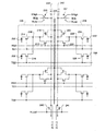
- 画像センサであって、
(a)基板上に行および列に配置された複数の画素を備えており、
各画素が、
(i)入射光に反応して電荷を収集する少なくとも一つの感光性領域と、
(ii)前記少なくとも一つの感光性領域から前記電荷を感知し、前記電荷を電圧に変換する電荷・電圧変換ノードと、
(iii)出力ノードに接続されたソースを有し、前記電荷・電圧変換ノードに接続されたゲートを有し、電源ノードの一部に接続されたドレインを有する増幅器トランジスタであって、隣接する列の画素は前記電源ノードの残りの部分に接続されたドレインを有する増幅器トランジスタを含む、増幅器トランジスタと、
(iv)前記出力ノードと前記電荷・電圧変換ノードとを接続するリセットトランジスタと、
を備え、
1つの列内の各画素に含まれる、前記電荷・電圧変換ノード、前記リセットトランジスタのリセットゲート、前記出力ノード、前記増幅器トランジスタのゲート、および前記電源ノードの一部は、
前記隣接する列に向かう方向に、前記電荷・電圧変換ノード、前記リセットトランジスタのリセットゲート、前記出力ノード、前記増幅器トランジスタのゲート、および前記電源ノードの一部、という空間的順序で配置されており、
前記隣接する列内の各画素に含まれる、前記電源ノードの残りの部分、前記増幅器トランジスタのゲート、前記出力ノード、前記リセットトランジスタのリセットゲート、および前記電荷・電圧変換ノードは、
前記1つの列から離れる方向に、前記電源ノードの残りの部分、前記増幅器トランジスタのゲート、前記出力ノード、前記リセットトランジスタのリセットゲート、および前記電荷・電圧変換ノード、という空間的順序で配置されている、
画素センサ。 - 各画素が、各感光性領域から前記電荷・電圧変換ノードへ電荷を転送する転送ゲートを含む、請求項1に記載の画像センサ。
- 前記1つの列内の各画素、および前記隣接する列内の各画素は、
隣接する二つの感光性領域を備え、
前記二つの感光性領域のそれぞれは、転送ゲートを備え、
各転送ゲートは、前記二つの感光性領域に共有される前記電荷・電圧変換ノードに接続されている、請求項1に記載の画像センサ。 - 前記画素センサは撮像装置内に設けられる、請求項1から3のいずれか1項に記載の画像センサ。
Applications Claiming Priority (3)
| Application Number | Priority Date | Filing Date | Title |
|---|---|---|---|
| US11/686,573 US7915702B2 (en) | 2007-03-15 | 2007-03-15 | Reduced pixel area image sensor |
| US11/686,573 | 2007-03-15 | ||
| PCT/US2008/002235 WO2008115331A1 (en) | 2007-03-15 | 2008-02-20 | Reduced pixel area image sensor |
Publications (3)
| Publication Number | Publication Date |
|---|---|
| JP2010521812A JP2010521812A (ja) | 2010-06-24 |
| JP2010521812A5 JP2010521812A5 (ja) | 2011-04-14 |
| JP5357063B2 true JP5357063B2 (ja) | 2013-12-04 |
Family
ID=39491702
Family Applications (1)
| Application Number | Title | Priority Date | Filing Date |
|---|---|---|---|
| JP2009553578A Active JP5357063B2 (ja) | 2007-03-15 | 2008-02-20 | 画像センサ |
Country Status (8)
| Country | Link |
|---|---|
| US (2) | US7915702B2 (ja) |
| EP (1) | EP2118930B1 (ja) |
| JP (1) | JP5357063B2 (ja) |
| KR (1) | KR101398767B1 (ja) |
| CN (2) | CN102623474B (ja) |
| HK (1) | HK1171870A1 (ja) |
| TW (2) | TWI559514B (ja) |
| WO (1) | WO2008115331A1 (ja) |
Families Citing this family (22)
| Publication number | Priority date | Publication date | Assignee | Title |
|---|---|---|---|---|
| US7924333B2 (en) * | 2007-08-17 | 2011-04-12 | Aptina Imaging Corporation | Method and apparatus providing shared pixel straight gate architecture |
| US7989749B2 (en) * | 2007-10-05 | 2011-08-02 | Aptina Imaging Corporation | Method and apparatus providing shared pixel architecture |
| JP5408954B2 (ja) * | 2008-10-17 | 2014-02-05 | キヤノン株式会社 | 撮像装置、及び撮像システム |
| GB2466213B (en) * | 2008-12-12 | 2013-03-06 | Cmosis Nv | Pixel array with shared readout circuitry |
| JP5029624B2 (ja) * | 2009-01-15 | 2012-09-19 | ソニー株式会社 | 固体撮像装置及び電子機器 |
| JP2010206172A (ja) * | 2009-02-06 | 2010-09-16 | Canon Inc | 撮像装置およびカメラ |
| JP2010206173A (ja) | 2009-02-06 | 2010-09-16 | Canon Inc | 光電変換装置およびカメラ |
| JP2010206174A (ja) | 2009-02-06 | 2010-09-16 | Canon Inc | 光電変換装置およびその製造方法ならびにカメラ |
| JP5564874B2 (ja) * | 2009-09-25 | 2014-08-06 | ソニー株式会社 | 固体撮像装置、及び電子機器 |
| JP5537172B2 (ja) * | 2010-01-28 | 2014-07-02 | ソニー株式会社 | 固体撮像装置及び電子機器 |
| JP5377549B2 (ja) * | 2011-03-03 | 2013-12-25 | 株式会社東芝 | 固体撮像装置 |
| US9766202B2 (en) | 2011-07-14 | 2017-09-19 | National University Corporation Toyohashi University Of Technology | Method for detecting chemical and physical phenomenon, and device therefor |
| DE102011120099B4 (de) | 2011-12-02 | 2024-05-29 | Arnold & Richter Cine Technik Gmbh & Co. Betriebs Kg | Bildsensor und Verfahren zum Auslesen eines Bildsensors |
| CN103208501B (zh) | 2012-01-17 | 2017-07-28 | 奥林巴斯株式会社 | 固体摄像装置及其制造方法、摄像装置、基板、半导体装置 |
| JP5953087B2 (ja) * | 2012-01-17 | 2016-07-13 | オリンパス株式会社 | 固体撮像装置、撮像装置および固体撮像装置の製造方法 |
| WO2014002366A1 (ja) * | 2012-06-27 | 2014-01-03 | パナソニック株式会社 | 固体撮像装置 |
| JP5962533B2 (ja) * | 2013-02-13 | 2016-08-03 | ソニー株式会社 | 固体撮像素子、駆動方法、および撮像装置 |
| US9319613B2 (en) * | 2013-12-05 | 2016-04-19 | Omnivision Technologies, Inc. | Image sensor having NMOS source follower with P-type doping in polysilicon gate |
| CN105100654B (zh) * | 2015-09-18 | 2018-02-23 | 中国科学院高能物理研究所 | 一种像素单元电路及像素读出芯片 |
| KR20180076845A (ko) | 2016-12-28 | 2018-07-06 | 삼성전자주식회사 | 이미지 센서 |
| KR20210114786A (ko) * | 2020-03-11 | 2021-09-24 | 에스케이하이닉스 주식회사 | 이미지 센서 |
| WO2023137680A1 (en) * | 2022-01-21 | 2023-07-27 | Huawei Technologies Co.,Ltd. | Imaging device array |
Family Cites Families (21)
| Publication number | Priority date | Publication date | Assignee | Title |
|---|---|---|---|---|
| US5625210A (en) | 1995-04-13 | 1997-04-29 | Eastman Kodak Company | Active pixel sensor integrated with a pinned photodiode |
| ES2211937T3 (es) | 1995-08-02 | 2004-07-16 | Canon Kabushiki Kaisha | Dispositivo sensor de imagenes de estado solido con linea de salida comun. |
| EP0809394B1 (en) * | 1996-05-22 | 2008-02-13 | Eastman Kodak Company | Active pixel sensor with switched supply row select |
| US5949061A (en) | 1997-02-27 | 1999-09-07 | Eastman Kodak Company | Active pixel sensor with switched supply row select |
| US5903021A (en) * | 1997-01-17 | 1999-05-11 | Eastman Kodak Company | Partially pinned photodiode for solid state image sensors |
| US6160281A (en) | 1997-02-28 | 2000-12-12 | Eastman Kodak Company | Active pixel sensor with inter-pixel function sharing |
| US6107655A (en) * | 1997-08-15 | 2000-08-22 | Eastman Kodak Company | Active pixel image sensor with shared amplifier read-out |
| JP3466886B2 (ja) * | 1997-10-06 | 2003-11-17 | キヤノン株式会社 | 固体撮像装置 |
| JP4006111B2 (ja) | 1998-09-28 | 2007-11-14 | キヤノン株式会社 | 固体撮像装置 |
| US6624850B1 (en) * | 1998-12-30 | 2003-09-23 | Eastman Kodak Company | Photogate active pixel sensor with high fill factor and correlated double sampling |
| US6218656B1 (en) * | 1998-12-30 | 2001-04-17 | Eastman Kodak Company | Photodiode active pixel sensor with shared reset signal row select |
| US6657665B1 (en) | 1998-12-31 | 2003-12-02 | Eastman Kodak Company | Active Pixel Sensor with wired floating diffusions and shared amplifier |
| US6541794B1 (en) * | 2000-08-31 | 2003-04-01 | Motorola, Inc. | Imaging device and method |
| CN100347859C (zh) * | 2001-03-05 | 2007-11-07 | 松下电器产业株式会社 | 固体摄象装置 |
| US6855937B2 (en) * | 2001-05-18 | 2005-02-15 | Canon Kabushiki Kaisha | Image pickup apparatus |
| US6720942B2 (en) * | 2002-02-12 | 2004-04-13 | Eastman Kodak Company | Flat-panel light emitting pixel with luminance feedback |
| US7183531B2 (en) * | 2004-03-31 | 2007-02-27 | Micron Technology, Inc. | Amplification with feedback capacitance for photodetector signals |
| US20060103749A1 (en) * | 2004-11-12 | 2006-05-18 | Xinping He | Image sensor and pixel that has switchable capacitance at the floating node |
| JP4340660B2 (ja) | 2005-04-14 | 2009-10-07 | シャープ株式会社 | 増幅型固体撮像装置 |
| JP4768305B2 (ja) | 2005-04-15 | 2011-09-07 | 岩手東芝エレクトロニクス株式会社 | 固体撮像装置 |
| JP5247007B2 (ja) | 2005-06-09 | 2013-07-24 | キヤノン株式会社 | 撮像装置及び撮像システム |
-
2007
- 2007-03-15 US US11/686,573 patent/US7915702B2/en active Active
-
2008
- 2008-02-20 JP JP2009553578A patent/JP5357063B2/ja active Active
- 2008-02-20 WO PCT/US2008/002235 patent/WO2008115331A1/en active Application Filing
- 2008-02-20 CN CN201210102673.9A patent/CN102623474B/zh active Active
- 2008-02-20 KR KR1020097019118A patent/KR101398767B1/ko active IP Right Grant
- 2008-02-20 CN CN2008800084283A patent/CN101647118B/zh active Active
- 2008-02-20 EP EP08725828.1A patent/EP2118930B1/en active Active
- 2008-03-14 TW TW102139161A patent/TWI559514B/zh active
- 2008-03-14 TW TW097109186A patent/TWI418021B/zh active
-
2011
- 2011-01-26 US US13/014,336 patent/US8294187B2/en active Active
-
2012
- 2012-12-07 HK HK12112671.7A patent/HK1171870A1/xx unknown
Also Published As
| Publication number | Publication date |
|---|---|
| US20080225148A1 (en) | 2008-09-18 |
| WO2008115331A1 (en) | 2008-09-25 |
| US8294187B2 (en) | 2012-10-23 |
| JP2010521812A (ja) | 2010-06-24 |
| US20110122307A1 (en) | 2011-05-26 |
| KR20090121322A (ko) | 2009-11-25 |
| US7915702B2 (en) | 2011-03-29 |
| TW201407759A (zh) | 2014-02-16 |
| CN102623474A (zh) | 2012-08-01 |
| CN101647118A (zh) | 2010-02-10 |
| TWI559514B (zh) | 2016-11-21 |
| CN102623474B (zh) | 2015-08-05 |
| TW200903789A (en) | 2009-01-16 |
| EP2118930B1 (en) | 2015-01-14 |
| KR101398767B1 (ko) | 2014-05-27 |
| EP2118930A1 (en) | 2009-11-18 |
| HK1171870A1 (en) | 2013-04-05 |
| CN101647118B (zh) | 2012-06-27 |
| TWI418021B (zh) | 2013-12-01 |
Similar Documents
| Publication | Publication Date | Title |
|---|---|---|
| JP5357063B2 (ja) | 画像センサ | |
| KR100718781B1 (ko) | 콤팩트 픽셀 레이아웃을 갖는 cmos 이미지 센서 | |
| US7307300B2 (en) | Solid-state image pick-up device and imaging system using the same | |
| JP4752447B2 (ja) | 固体撮像装置およびカメラ | |
| US7244918B2 (en) | Method and apparatus providing a two-way shared storage gate on a four-way shared pixel | |
| US20050128327A1 (en) | Device and method for image sensing | |
| EP2150038B1 (en) | Image sensor pixel with gain control | |
| US7265397B1 (en) | CCD imager constructed with CMOS fabrication techniques and back illuminated imager with improved light capture | |
| KR20090056846A (ko) | 고체 촬상 소자 및 카메라 | |
| KR100820520B1 (ko) | 고체촬상장치 | |
| TW201103340A (en) | Solid-state imaging device and electronic apparatus | |
| KR100801758B1 (ko) | 이미지 센서 및 그 제어 방법 | |
| US11011569B2 (en) | Image sensor including a plurality of transfer transistors coupled between photodiode and floating diffusion region | |
| KR100769563B1 (ko) | 누설 전류를 감소시킨 이미지 센서 | |
| US8785986B1 (en) | BCMD image sensor with junction gate for back side or front side illumination |
Legal Events
| Date | Code | Title | Description |
|---|---|---|---|
| A521 | Request for written amendment filed |
Free format text: JAPANESE INTERMEDIATE CODE: A523 Effective date: 20110217 |
|
| A621 | Written request for application examination |
Free format text: JAPANESE INTERMEDIATE CODE: A621 Effective date: 20110217 |
|
| A521 | Request for written amendment filed |
Free format text: JAPANESE INTERMEDIATE CODE: A523 Effective date: 20110719 |
|
| A711 | Notification of change in applicant |
Free format text: JAPANESE INTERMEDIATE CODE: A711 Effective date: 20110719 |
|
| A131 | Notification of reasons for refusal |
Free format text: JAPANESE INTERMEDIATE CODE: A131 Effective date: 20121030 |
|
| A977 | Report on retrieval |
Free format text: JAPANESE INTERMEDIATE CODE: A971007 Effective date: 20121031 |
|
| A521 | Request for written amendment filed |
Free format text: JAPANESE INTERMEDIATE CODE: A523 Effective date: 20130123 |
|
| TRDD | Decision of grant or rejection written | ||
| A01 | Written decision to grant a patent or to grant a registration (utility model) |
Free format text: JAPANESE INTERMEDIATE CODE: A01 Effective date: 20130820 |
|
| A61 | First payment of annual fees (during grant procedure) |
Free format text: JAPANESE INTERMEDIATE CODE: A61 Effective date: 20130829 |
|
| R150 | Certificate of patent or registration of utility model |
Ref document number: 5357063 Country of ref document: JP Free format text: JAPANESE INTERMEDIATE CODE: R150 Free format text: JAPANESE INTERMEDIATE CODE: R150 |
|
| R250 | Receipt of annual fees |
Free format text: JAPANESE INTERMEDIATE CODE: R250 |
|
| R250 | Receipt of annual fees |
Free format text: JAPANESE INTERMEDIATE CODE: R250 |
|
| R250 | Receipt of annual fees |
Free format text: JAPANESE INTERMEDIATE CODE: R250 |
|
| R250 | Receipt of annual fees |
Free format text: JAPANESE INTERMEDIATE CODE: R250 |
|
| R250 | Receipt of annual fees |
Free format text: JAPANESE INTERMEDIATE CODE: R250 |
|
| R250 | Receipt of annual fees |
Free format text: JAPANESE INTERMEDIATE CODE: R250 |
|
| R250 | Receipt of annual fees |
Free format text: JAPANESE INTERMEDIATE CODE: R250 |
|
| R250 | Receipt of annual fees |
Free format text: JAPANESE INTERMEDIATE CODE: R250 |