EP2118930B1 - Reduced pixel area image sensor - Google Patents
Reduced pixel area image sensor Download PDFInfo
- Publication number
- EP2118930B1 EP2118930B1 EP08725828.1A EP08725828A EP2118930B1 EP 2118930 B1 EP2118930 B1 EP 2118930B1 EP 08725828 A EP08725828 A EP 08725828A EP 2118930 B1 EP2118930 B1 EP 2118930B1
- Authority
- EP
- European Patent Office
- Prior art keywords
- pixel
- charge
- gate
- image sensor
- reset
- Prior art date
- Legal status (The legal status is an assumption and is not a legal conclusion. Google has not performed a legal analysis and makes no representation as to the accuracy of the status listed.)
- Active
Links
Images

Classifications
-
- H—ELECTRICITY
- H10—SEMICONDUCTOR DEVICES; ELECTRIC SOLID-STATE DEVICES NOT OTHERWISE PROVIDED FOR
- H10F—INORGANIC SEMICONDUCTOR DEVICES SENSITIVE TO INFRARED RADIATION, LIGHT, ELECTROMAGNETIC RADIATION OF SHORTER WAVELENGTH OR CORPUSCULAR RADIATION
- H10F39/00—Integrated devices, or assemblies of multiple devices, comprising at least one element covered by group H10F30/00, e.g. radiation detectors comprising photodiode arrays
- H10F39/80—Constructional details of image sensors
- H10F39/813—Electronic components shared by multiple pixels, e.g. one amplifier shared by two pixels
-
- H—ELECTRICITY
- H04—ELECTRIC COMMUNICATION TECHNIQUE
- H04N—PICTORIAL COMMUNICATION, e.g. TELEVISION
- H04N25/00—Circuitry of solid-state image sensors [SSIS]; Control thereof
-
- H—ELECTRICITY
- H04—ELECTRIC COMMUNICATION TECHNIQUE
- H04N—PICTORIAL COMMUNICATION, e.g. TELEVISION
- H04N25/00—Circuitry of solid-state image sensors [SSIS]; Control thereof
- H04N25/70—SSIS architectures; Circuits associated therewith
- H04N25/76—Addressed sensors, e.g. MOS or CMOS sensors
- H04N25/77—Pixel circuitry, e.g. memories, A/D converters, pixel amplifiers, shared circuits or shared components
- H04N25/778—Pixel circuitry, e.g. memories, A/D converters, pixel amplifiers, shared circuits or shared components comprising amplifiers shared between a plurality of pixels, i.e. at least one part of the amplifier must be on the sensor array itself
-
- H—ELECTRICITY
- H10—SEMICONDUCTOR DEVICES; ELECTRIC SOLID-STATE DEVICES NOT OTHERWISE PROVIDED FOR
- H10F—INORGANIC SEMICONDUCTOR DEVICES SENSITIVE TO INFRARED RADIATION, LIGHT, ELECTROMAGNETIC RADIATION OF SHORTER WAVELENGTH OR CORPUSCULAR RADIATION
- H10F39/00—Integrated devices, or assemblies of multiple devices, comprising at least one element covered by group H10F30/00, e.g. radiation detectors comprising photodiode arrays
- H10F39/80—Constructional details of image sensors
- H10F39/802—Geometry or disposition of elements in pixels, e.g. address-lines or gate electrodes
-
- H—ELECTRICITY
- H10—SEMICONDUCTOR DEVICES; ELECTRIC SOLID-STATE DEVICES NOT OTHERWISE PROVIDED FOR
- H10F—INORGANIC SEMICONDUCTOR DEVICES SENSITIVE TO INFRARED RADIATION, LIGHT, ELECTROMAGNETIC RADIATION OF SHORTER WAVELENGTH OR CORPUSCULAR RADIATION
- H10F39/00—Integrated devices, or assemblies of multiple devices, comprising at least one element covered by group H10F30/00, e.g. radiation detectors comprising photodiode arrays
- H10F39/80—Constructional details of image sensors
- H10F39/803—Pixels having integrated switching, control, storage or amplification elements
Definitions
- the invention relates generally to the field of CMOS active pixel image sensors and, more particularly, to reducing the size of a pixel.
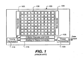
- Fig. 1 shows the typical CMOS active pixel image sensor 100.
- the basic component of the image sensor 100 is the array of photosensitive pixels 130.
- the row decoder circuitry 105 selects an entire row of pixels 130 to be sampled by the correlated double sampling (CDS) circuitry 125.
- the analog-to-digital converter 115 scans across the column decoders and digitizes the signals stored in the CDS 125.
- the analog-to-digital converter 115 may be of the type which has one converter for each column (parallel) or one high-speed converter to digitize each column serially.
- the digitized data may be directly output from the image sensor 100 or there may be integrated image processing 120 for defect correction, color filter interpolation, image scaling, and other special effects.
- the timing generator 110 controls the row and column decoders to sample the entire pixel array or only a portion of the pixel array.
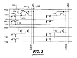
- Fig. 2 shows one of many different possible schematics for a CMOS image sensor.
- Four pixels 130 (only one is labeled for clarity) are shown of the pixel array.
- Each pixel 130 has circuitry that is shared between two photodiodes 150 and 151. This type of pixel along with other variations may be found in US Patents 5,625,210 ; 5,841,159 ; 5,949,061 ; 6,107,655 ; 6,160,281 ; 6,423,994 ; and 6,657,665 .
- the photodiodes 150 and 151 are connected to a common shared floating diffusion 155 respectively by transfer gates 152 and 153.
- the process of sampling the photodiode 150 begins by turning on the power supply (VDD) 158 and also turning on the reset transistor 154 to set the floating diffusion 155 voltage to the voltage of the power supply 158.
- the reset transistor 154 is then turned off, and the signal level sampled by the output transistor 156 is driven onto the output signal line 157.
- the transfer gate 153 is turned on to transfer photo-generated signal charge from photodiode 150 to the floating diffusion 155. Now the output transistor 156 will drive the signal level voltage onto the output signal line 157.
- the difference of the first signal just after reset minus the signal after the transfer gate 153 was pulsed is proportional to the number of electrons that was in the photodiode 150.
- the second photodiode 151 is sampled in the same manner through transfer gate 152.
- This pixel 130 is shown as a two-shared pixel because two photodiodes 150 and 151 share a common floating diffusion 155.
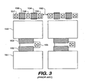
- An example of how a two-shared pixel might physically be manufactured on a silicon substrate is shown in Fig. 3 .
- the numbered components in Fig. 3 correspond to the schematic symbols in Fig. 2 .
- the polysilicon transistors transfer gates are 152 and 153; the reset transistor gate is 154 and the output transistor gate is 156.
- the floating diffusion contacts 155 are connected together by a metal wire.
- the reset 154 and output 156 transistors share a common diffusion connection 158 to the power supply line.
- the drawback with the pixel layout of Fig. 3 is how to reduce the size of the pixel.
- the gap 160 between two adjacent pixels cannot be shrunk further without risking leakage of electrons between to adjacent pixels.
- the size of the transistor gates 154 and 156 cannot shrink because the operating voltage of the power supply determines their size. Reducing the power supply voltage is not an attractive option because that also will reduce the maximum number of photoelectrons that can be collected by the photodiodes.
- the present invention will address this shortcoming and others as it discloses a way to reduce the pixel size without having to reduce the size of the reset and output transistor gates.
- the present invention is directed to overcoming one or more of the problems set forth above. Briefly summarized, the invention resides in an image sensor as defined by claim 1. Possible additional features appear in dependent claims.
- the invention allows for reducing an image sensor pixel size without reducing the size of the transistor geometry.
- CMOS complementary metal oxide silicon type electrical components such as transistors which are associated with the pixel, but typically not in the pixel, and which are formed when the source/drain of a transistor is of one dopant type (p-type for example) and its mated transistor is of the opposite dopant type (n-type).
- CMOS devices include some advantages one of which is it consumes less power.
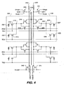
- the schematic for the pixel of the present invention is shown in Fig. 4 .
- the primary difference of this pixel 235 from the prior art is the reset transistor 212 is connected between the floating diffusion 218 and the output signal line 242.
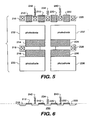
- the prior art would have connected the reset transistor to the power supply line (VDD) 234. While this schematic does not reduce the total number of transistors, it does allow the power supply line (VDD) 234 diffusions to be shared between two pixels 235 and 236. This is more clearly shown in Fig. 5 .
- Pixel 235 will be used as a representative pixel.
- pixel 235 includes two photosensitive areas or photodiodes 232 and 233 each for collecting charge in response to incident light. It is noted for clarity that pinned photodiodes could also be used as it is understood that this feature needs primarily to just collect charge in response to light.
- Transfer gate 214 transfers the charge from the photodiode 232 to the charge-to-voltage conversion node or sense node 218.
- An output transistor or amplifier 210 is connected to the sense node 218 via its gate, and the amplifier 210 senses the signal on the sense node 218 and outputs the signal on an output bus 242 via its source.
- the drain of the amplifier 210 is connected to the power supply (VDD) 234. This connection includes connecting the drain to at least a portion of the power supply node 234. This portion preferably includes one half or substantially one half of the power supply node 234.
- Amplifier 220 is connected in the same manner and is connected to the remaining portion of the power supply 234.
- Pixel 235 shares the sense node 218, amplifier 210 and reset transistor 212, but includes a separate photodiode 233 that collects charge in response to incident light and transfer gate 216 that transfers the charge to the sense node 218.
- An adjacent pixel 236 includes the same components as pixel 235, but are numbered differently for clarity.
- pixel 236 includes a photodiode 237, transfer gate 224, sense node or floating diffusion 228, amplifier 220 and reset transistor 222.
- Pixel 236 shares the floating diffusion 228, amplifier 220 and reset transistor 222, but includes a separate photodiode 238 and transfer gate 226.
- Pixel 235 (shown in Fig. 4 ) includes a sequential spatial order as follows: the charge-to-voltage conversion node 218, a reset gate of the reset transistor 212, the output node 242, a gate of the amplifier transistor 210 and at least a portion of the power supply node 234.
- the adjacent pixel 236 (also shown in Fig.
- the process of reading out charge from the row of photodiodes 232 and 237 begins by activating the floating diffusions 218 and 228. This is done by turning off the constant current sink load transistors 240 and 241 (see bottom of Fig. 4 ). With the load transistors 240 and 241 off, the switches 230 and 231 can be set to the VHigh voltage setting. Now when the reset transistors 212 and 222 are turned on, the floating diffusions 218 and 228 will be set to the VHigh voltage. Next, the reset transistors 212 and 222 are turned off and the switches 230 and 231 are set to the open setting.
- the current sink load transistors 240 and 241 are turned on so the output transistors 210 and 220 will drive the output lines 242 and 243 to a voltage representing the floating reset level corresponding to zero electrons of photo-signal.
- the transfer gates 214 and 224 are pulsed on and off to transfer the photo-generated charge from the photodiodes 232 and 237 to the floating diffusions 218 and 228.
- the output transistors 210 and 220 will drive the output lines 242 and 243 to a voltage level corresponding to the number of electrons generated in the photodiodes 232 and 237. The difference between this voltage level and the reset voltage level is proportional to the amount of charge in the photodiodes.
- the process is repeated by activating the floating diffusions 218 and 228. This is done by turning off the constant current sink load transistors 240 and 241. With the load transistors 240 and 241 off, the switches 230 and 231 can be set to the VHigh voltage setting. Now when the reset transistors 212 and 222 are turned on, the floating diffusions 218 and 228 will be set to the VHigh voltage. Next, the reset transistors 212 and 222 are turned off and the switches 230 and 231 are set to the open setting.
- the current sink load transistors 240 and 241 are turned on so the output transistors 210 and 220 will drive the output lines 242 and 243 to a voltage representing the floating reset level corresponding to zero electrons of photo-signal.
- the transfer gates 216 and 226 are pulsed on and off to transfer the photo-generated charge from the photodiodes 233 and 238 to the floating diffusions 218 and 228.
- the output transistors 210 and 220 will drive the output lines 242 and 243 to a voltage level corresponding to the number of electrons generated in the photodiodes 233 and 238. The difference between this voltage level and the reset voltage level is proportional to the amount of charge in the photodiodes.
- the transistors in pixels 235 and 236 must be de-activated before moving on to read out another row of pixels. Holding the reset transistors 212 and 222 in the on state sets the gate and source voltages equal of the output transistors 210 and 220. When the gate and source voltages are equal in a surface channel transistor the transistors will be in the off state. When the output transistors 210 and 220 are in the off state, they will not interfere with reading out photodiodes of other image sensor rows.
- Fig. 6 shows a cross section through the line of transistor gates 212, 210, 220, and 222.
- the transistors are fabricated in a silicon substrate 250.
- the pixel 235 in Fig. 4 shows two photodiodes 232 and 233 that share a common floating diffusion 218.
- CMOS image sensors will easily observe the invention can be applied to any number of photodiodes sharing or not sharing a common floating diffusion, including the case of no shared photodiodes.
- Fig. 4 also shows the VDD power supply line 234 oriented in the vertical direction.
- the power supply line 234 can also be oriented horizontally or in both directions as a square grid. Furthermore, if the VDD power supply line 234 is oriented horizontally it can be used to select or de-select rows for read out as in US Patents 5,949,061 and 6,323,476 .
- Fig. 7 shows the pixel of the present invention 330 incorporated into an image sensor 300.
- the image sensor 300 has row decoders 305 selecting and de-selecting rows for read out. It also has column decoders 325 for sampling the output lines of each column and an analog-to-digital converter 315 to digitize the signal on the output lines.
- the timing generator 310 controls the scanning of the row 305 and column 325 decoders.
- the image processor 320 is used to correct row and column gain and offsets as well as defected correction and color filter interpolation or other image processing functions.
- Fig. 8 is a digital camera 400 having the image sensor 300 of the present invention.
Landscapes
- Engineering & Computer Science (AREA)
- Multimedia (AREA)
- Signal Processing (AREA)
- Solid State Image Pick-Up Elements (AREA)
- Transforming Light Signals Into Electric Signals (AREA)
Description
- The invention relates generally to the field of CMOS active pixel image sensors and, more particularly, to reducing the size of a pixel.
-
Fig. 1 shows the typical CMOS activepixel image sensor 100. The basic component of theimage sensor 100 is the array ofphotosensitive pixels 130. Therow decoder circuitry 105 selects an entire row ofpixels 130 to be sampled by the correlated double sampling (CDS)circuitry 125. The analog-to-digital converter 115 scans across the column decoders and digitizes the signals stored in theCDS 125. The analog-to-digital converter 115 may be of the type which has one converter for each column (parallel) or one high-speed converter to digitize each column serially. The digitized data may be directly output from theimage sensor 100 or there may be integratedimage processing 120 for defect correction, color filter interpolation, image scaling, and other special effects. Thetiming generator 110 controls the row and column decoders to sample the entire pixel array or only a portion of the pixel array. -
Fig. 2 shows one of many different possible schematics for a CMOS image sensor. Four pixels 130 (only one is labeled for clarity) are shown of the pixel array. Eachpixel 130 has circuitry that is shared between twophotodiodes US Patents 5,625,210 ;5,841,159 ;5,949,061 ;6,107,655 ;6,160,281 ;6,423,994 ; and6,657,665 . - The
photodiodes diffusion 155 respectively bytransfer gates photodiode 150 begins by turning on the power supply (VDD) 158 and also turning on thereset transistor 154 to set thefloating diffusion 155 voltage to the voltage of thepower supply 158. Thereset transistor 154 is then turned off, and the signal level sampled by theoutput transistor 156 is driven onto theoutput signal line 157. Next, thetransfer gate 153 is turned on to transfer photo-generated signal charge fromphotodiode 150 to thefloating diffusion 155. Now theoutput transistor 156 will drive the signal level voltage onto theoutput signal line 157. The difference of the first signal just after reset minus the signal after thetransfer gate 153 was pulsed is proportional to the number of electrons that was in thephotodiode 150. - The
second photodiode 151 is sampled in the same manner throughtransfer gate 152. Thispixel 130 is shown as a two-shared pixel because twophotodiodes diffusion 155. An example of how a two-shared pixel might physically be manufactured on a silicon substrate is shown inFig. 3 . The numbered components inFig. 3 correspond to the schematic symbols inFig. 2 . The polysilicon transistors transfer gates are 152 and 153; the reset transistor gate is 154 and the output transistor gate is 156. Thefloating diffusion contacts 155 are connected together by a metal wire. Thereset 154 andoutput 156 transistors share acommon diffusion connection 158 to the power supply line. - The drawback with the pixel layout of
Fig. 3 is how to reduce the size of the pixel. Thegap 160 between two adjacent pixels cannot be shrunk further without risking leakage of electrons between to adjacent pixels. The size of thetransistor gates - The present invention will address this shortcoming and others as it discloses a way to reduce the pixel size without having to reduce the size of the reset and output transistor gates.
- The present invention is directed to overcoming one or more of the problems set forth above. Briefly summarized, the invention resides in an image sensor as defined by
claim 1. Possible additional features appear in dependent claims. - The invention allows for reducing an image sensor pixel size without reducing the size of the transistor geometry.
-
-
Fig. 1 is a prior art active pixel image sensor; -
Fig. 2 is a schematic diagram of a pixel ofFig. 1 ; -
Fig. 3 is a plan view (top view) ofFig. 1 ; -
Fig. 4 is a schematic diagram of a plurality of pixels of the present invention; -
Fig. 5 is a plan view (top view) ofFig. 4 ; -
Fig. 6 a horizontal cross-section through the transistors ofFig. 5 ; -
Fig. 7 is the image sensor of the present invention having the pixels ofFig. 4 ; and -
Fig. 8 is a camera having the image sensor of the present invention. - Before discussing the present invention in detail, it is instructive to note that the present invention is preferably used in, but not limited to, a CMOS active pixel sensor. Active pixel sensor refers to an active electrical element within the pixel, more specifically the amplifier, and CMOS refers to complementary metal oxide silicon type electrical components such as transistors which are associated with the pixel, but typically not in the pixel, and which are formed when the source/drain of a transistor is of one dopant type (p-type for example) and its mated transistor is of the opposite dopant type (n-type). CMOS devices include some advantages one of which is it consumes less power.
- To reduce the pixel size, it is necessary to change the operation of the transistors in the pixels. The schematic for the pixel of the present invention is shown in
Fig. 4 . The primary difference of thispixel 235 from the prior art is thereset transistor 212 is connected between thefloating diffusion 218 and theoutput signal line 242. The prior art would have connected the reset transistor to the power supply line (VDD) 234. While this schematic does not reduce the total number of transistors, it does allow the power supply line (VDD) 234 diffusions to be shared between twopixels Fig. 5 . - Referring back to
Fig. 4 , each pixel will now be described in detail.Pixel 235 will be used as a representative pixel. In this regard,pixel 235 includes two photosensitive areas orphotodiodes Transfer gate 214 transfers the charge from thephotodiode 232 to the charge-to-voltage conversion node orsense node 218. An output transistor oramplifier 210, preferably a source follower, is connected to thesense node 218 via its gate, and theamplifier 210 senses the signal on thesense node 218 and outputs the signal on anoutput bus 242 via its source. The drain of theamplifier 210 is connected to the power supply (VDD) 234. This connection includes connecting the drain to at least a portion of thepower supply node 234. This portion preferably includes one half or substantially one half of thepower supply node 234.Amplifier 220 is connected in the same manner and is connected to the remaining portion of thepower supply 234.Pixel 235 shares thesense node 218,amplifier 210 and resettransistor 212, but includes aseparate photodiode 233 that collects charge in response to incident light andtransfer gate 216 that transfers the charge to thesense node 218. - An
adjacent pixel 236 includes the same components aspixel 235, but are numbered differently for clarity. In this regard,pixel 236 includes aphotodiode 237,transfer gate 224, sense node or floatingdiffusion 228,amplifier 220 and resettransistor 222.Pixel 236 shares the floatingdiffusion 228,amplifier 220 and resettransistor 222, but includes aseparate photodiode 238 andtransfer gate 226. - In
Fig. 5 , the reference numerals correspond to the numerals inFig. 4 . TheVDD diffusion 234 is shared between the twooutput transistors reset transistor gates outputs Fig. 4 ) includes a sequential spatial order as follows: the charge-to-voltage conversion node 218, a reset gate of thereset transistor 212, theoutput node 242, a gate of theamplifier transistor 210 and at least a portion of thepower supply node 234. The adjacent pixel 236 (also shown inFig. 4 ) includes a sequential spatial order as follows: a remaining portion of thepower supply node 234, a gate of theamplifier transistor 220, theoutput node 243, a reset gate of thereset transistor 222, and a charge-to-voltage conversion node 228. - Referring back to
Fig. 4 , the process of reading out charge from the row ofphotodiodes sink load transistors 240 and 241 (see bottom ofFig. 4 ). With theload transistors switches reset transistors reset transistors switches sink load transistors output transistors output lines transfer gates photodiodes output transistors output lines photodiodes - To read out the next row of
photodiodes sink load transistors load transistors switches reset transistors reset transistors switches sink load transistors output transistors output lines transfer gates photodiodes output transistors output lines photodiodes - Next the transistors in
pixels reset transistors output transistors output transistors - By sharing a common power supply (VDD)
diffusion 234, the amount of area occupied by the transistors is reduced inFig. 5 . Compared to the prior art inFig. 3 there is one less contact and one less isolation region between transistors. This allows the overall pixel size to be reduced while maintaining the same transistor gate dimensions and maintaining reasonable sized photodiodes. -
Fig. 6 shows a cross section through the line oftransistor gates silicon substrate 250. - The
pixel 235 inFig. 4 shows twophotodiodes diffusion 218. Those skilled in the art of CMOS image sensors will easily observe the invention can be applied to any number of photodiodes sharing or not sharing a common floating diffusion, including the case of no shared photodiodes. -
Fig. 4 also shows the VDDpower supply line 234 oriented in the vertical direction. Thepower supply line 234 can also be oriented horizontally or in both directions as a square grid. Furthermore, if the VDDpower supply line 234 is oriented horizontally it can be used to select or de-select rows for read out as inUS Patents 5,949,061 and6,323,476 . -
Fig. 7 shows the pixel of thepresent invention 330 incorporated into animage sensor 300. Theimage sensor 300 hasrow decoders 305 selecting and de-selecting rows for read out. It also hascolumn decoders 325 for sampling the output lines of each column and an analog-to-digital converter 315 to digitize the signal on the output lines. Thetiming generator 310 controls the scanning of therow 305 andcolumn 325 decoders. Theimage processor 320 is used to correct row and column gain and offsets as well as defected correction and color filter interpolation or other image processing functions. -
Fig. 8 is adigital camera 400 having theimage sensor 300 of the present invention. -
- 100
- image sensor
- 105
- row decoder circuitry
- 110
- timing generator
- 115
- analog-to-digital converter
- 120
- image processing
- 125
- correlated double sampling (CDS) circuitry
- 130
- photosensitive pixel
- 150
- photodiode
- 151
- photodiode
- 152
- transfer gate
- 153
- transfer gate
- 154
- reset transistor gate
- 155
- floating diffusion
- 156
- output transistor gate
- 157
- output signal line
- 158
- power supply line (VDD)
- 160
- gap
- 210
- output transistor or amplifier
- 212
- reset transistor gate
- 214
- transfer gate
- 216
- transfer gate
- 218
- floating diffusion or sense node
- 220
- output transistor or amplifier
- 222
- reset transistor gate
- 224
- transfer gate
- 226
- transfer gate
- 228
- floating diffusion or sense node
- 230
- switches
- 231
- switches
- 232
- photodiode
- 233
- photodiode
- 234
- power supply line (VDD)
- 235
- pixel
- 236
- pixel
- 237
- photodiode
- 238
- photodiode
- 240
- sink load transistor
- 241
- sink load transistor
- 242
- output signal line
- 243
- output signal line
- 250
- silicon substrate
- 300
- image sensor
- 305
- row decoders
- 310
- timing generator
- 315
- analog-to-digital converter
- 320
- image processor
- 325
- column decoders
- 330
- photosensitive pixels
- 400
- digital camera
Claims (3)
- An image sensor (300) comprising:(a) a plurality of pixels disposed on a substrate and arranged in rows and columns, at least two adjacent pixels (235, 236) comprising only one power supply diffusion (234) and each pixel (235, 236) including:(i) at least one photosensitive region (232, 233, 237, 238) that collects charges in response to incident light;(ii) a charge-to-voltage conversion node (218, 228) for sensing the charge from the at least one photosensitive region (232, 233, 237, 238) and converting the charge to a voltage;(iii) an amplifier transistor (210, 220) having a source connected to an output node (242, 243), having a gate connected to the charge-to-voltage conversion node (218, 228) and having a drain connected to a portion of the a power supply diffusion (234); and(iv) a reset transistor (212, 222) for connecting the output node (242, 243) and the charge-to-voltage conversion node (218, 228),
characterized in that one pixel (235) of said at least two adjacent pixels includes a sequential spatial order as follows: the charge-to-voltage conversion node (218), a reset gate of the reset transistor (212), the output node (242), the gate of the amplifier transistor (210) and a portion of the power supply diffusion (234) and the adjacent pixel (236) of said at least two adjacent pixels includes a sequential spatial order as follows: a remaining portion of the power supply diffusion (234), the gate of the amplifier transistor (220), the output node (243), a reset gate of the reset transistor (222), and a charge-to-voltage conversion node (228). - The image sensor (300) as in claim 1, wherein each pixel (235, 236) includes a transfer gate (214, 216, 224, 226) for transferring charge from a respective photosensitive region (232, 233, 237, 238) to the charge-to-voltage conversion node (218, 228).
- The image sensor (300) as in claim 1, wherein the image sensor (300) is disposed in an image capture device (400).
Applications Claiming Priority (2)
| Application Number | Priority Date | Filing Date | Title |
|---|---|---|---|
| US11/686,573 US7915702B2 (en) | 2007-03-15 | 2007-03-15 | Reduced pixel area image sensor |
| PCT/US2008/002235 WO2008115331A1 (en) | 2007-03-15 | 2008-02-20 | Reduced pixel area image sensor |
Publications (2)
| Publication Number | Publication Date |
|---|---|
| EP2118930A1 EP2118930A1 (en) | 2009-11-18 |
| EP2118930B1 true EP2118930B1 (en) | 2015-01-14 |
Family
ID=39491702
Family Applications (1)
| Application Number | Title | Priority Date | Filing Date |
|---|---|---|---|
| EP08725828.1A Active EP2118930B1 (en) | 2007-03-15 | 2008-02-20 | Reduced pixel area image sensor |
Country Status (7)
| Country | Link |
|---|---|
| US (2) | US7915702B2 (en) |
| EP (1) | EP2118930B1 (en) |
| JP (1) | JP5357063B2 (en) |
| KR (1) | KR101398767B1 (en) |
| CN (2) | CN101647118B (en) |
| TW (2) | TWI559514B (en) |
| WO (1) | WO2008115331A1 (en) |
Families Citing this family (24)
| Publication number | Priority date | Publication date | Assignee | Title |
|---|---|---|---|---|
| US7924333B2 (en) * | 2007-08-17 | 2011-04-12 | Aptina Imaging Corporation | Method and apparatus providing shared pixel straight gate architecture |
| US7989749B2 (en) * | 2007-10-05 | 2011-08-02 | Aptina Imaging Corporation | Method and apparatus providing shared pixel architecture |
| JP5408954B2 (en) * | 2008-10-17 | 2014-02-05 | キヤノン株式会社 | Imaging apparatus and imaging system |
| GB2466213B (en) * | 2008-12-12 | 2013-03-06 | Cmosis Nv | Pixel array with shared readout circuitry |
| JP5029624B2 (en) * | 2009-01-15 | 2012-09-19 | ソニー株式会社 | Solid-state imaging device and electronic apparatus |
| JP2010206173A (en) | 2009-02-06 | 2010-09-16 | Canon Inc | Photoelectric conversion device and camera |
| JP2010206174A (en) | 2009-02-06 | 2010-09-16 | Canon Inc | Photoelectric converter, method of manufacturing the same, and camera |
| JP2010206172A (en) * | 2009-02-06 | 2010-09-16 | Canon Inc | Image sensing device, and camera |
| JP5564874B2 (en) * | 2009-09-25 | 2014-08-06 | ソニー株式会社 | Solid-state imaging device and electronic apparatus |
| JP5537172B2 (en) * | 2010-01-28 | 2014-07-02 | ソニー株式会社 | Solid-state imaging device and electronic apparatus |
| JP5377549B2 (en) * | 2011-03-03 | 2013-12-25 | 株式会社東芝 | Solid-state imaging device |
| WO2013008908A1 (en) * | 2011-07-14 | 2013-01-17 | 国立大学法人豊橋技術科学大学 | Method for detecting chemical and physical phenomenon, and device therefor |
| DE102011120099B4 (en) | 2011-12-02 | 2024-05-29 | Arnold & Richter Cine Technik Gmbh & Co. Betriebs Kg | Image sensor and method for reading an image sensor |
| CN103208501B (en) | 2012-01-17 | 2017-07-28 | 奥林巴斯株式会社 | Solid camera head and its manufacture method, camera device, substrate, semiconductor device |
| JP5953087B2 (en) * | 2012-01-17 | 2016-07-13 | オリンパス株式会社 | Solid-state imaging device, imaging device, and manufacturing method of solid-state imaging device |
| WO2014002366A1 (en) * | 2012-06-27 | 2014-01-03 | パナソニック株式会社 | Solid-state imaging device |
| JP5962533B2 (en) * | 2013-02-13 | 2016-08-03 | ソニー株式会社 | Solid-state imaging device, driving method, and imaging apparatus |
| US9319613B2 (en) * | 2013-12-05 | 2016-04-19 | Omnivision Technologies, Inc. | Image sensor having NMOS source follower with P-type doping in polysilicon gate |
| CN105100654B (en) * | 2015-09-18 | 2018-02-23 | 中国科学院高能物理研究所 | A kind of pixel unit circuit and pixel read chip |
| KR102701855B1 (en) | 2016-12-28 | 2024-09-02 | 삼성전자주식회사 | Image sensor |
| JP7467061B2 (en) * | 2019-10-09 | 2024-04-15 | 株式会社ジャパンディスプレイ | Detection device |
| KR102930839B1 (en) * | 2020-03-11 | 2026-02-26 | 에스케이하이닉스 주식회사 | Image Sensor |
| AU2022255719A1 (en) | 2021-04-08 | 2023-10-26 | Quantum-Si Incorporated | Integrated circuit having mirrored pixel configuration |
| CN117280470A (en) * | 2022-01-21 | 2023-12-22 | 华为技术有限公司 | Imaging device array |
Family Cites Families (21)
| Publication number | Priority date | Publication date | Assignee | Title |
|---|---|---|---|---|
| US5625210A (en) * | 1995-04-13 | 1997-04-29 | Eastman Kodak Company | Active pixel sensor integrated with a pinned photodiode |
| DE69631356T2 (en) | 1995-08-02 | 2004-07-15 | Canon K.K. | Semiconductor image sensor with common output power |
| US5949061A (en) * | 1997-02-27 | 1999-09-07 | Eastman Kodak Company | Active pixel sensor with switched supply row select |
| EP0809394B1 (en) * | 1996-05-22 | 2008-02-13 | Eastman Kodak Company | Active pixel sensor with switched supply row select |
| US5903021A (en) * | 1997-01-17 | 1999-05-11 | Eastman Kodak Company | Partially pinned photodiode for solid state image sensors |
| US6160281A (en) * | 1997-02-28 | 2000-12-12 | Eastman Kodak Company | Active pixel sensor with inter-pixel function sharing |
| US6107655A (en) * | 1997-08-15 | 2000-08-22 | Eastman Kodak Company | Active pixel image sensor with shared amplifier read-out |
| JP3466886B2 (en) * | 1997-10-06 | 2003-11-17 | キヤノン株式会社 | Solid-state imaging device |
| JP4006111B2 (en) * | 1998-09-28 | 2007-11-14 | キヤノン株式会社 | Solid-state imaging device |
| US6624850B1 (en) * | 1998-12-30 | 2003-09-23 | Eastman Kodak Company | Photogate active pixel sensor with high fill factor and correlated double sampling |
| US6218656B1 (en) * | 1998-12-30 | 2001-04-17 | Eastman Kodak Company | Photodiode active pixel sensor with shared reset signal row select |
| US6657665B1 (en) * | 1998-12-31 | 2003-12-02 | Eastman Kodak Company | Active Pixel Sensor with wired floating diffusions and shared amplifier |
| US6541794B1 (en) * | 2000-08-31 | 2003-04-01 | Motorola, Inc. | Imaging device and method |
| CN100347859C (en) * | 2001-03-05 | 2007-11-07 | 松下电器产业株式会社 | solid state imaging device |
| US6855937B2 (en) * | 2001-05-18 | 2005-02-15 | Canon Kabushiki Kaisha | Image pickup apparatus |
| US6720942B2 (en) * | 2002-02-12 | 2004-04-13 | Eastman Kodak Company | Flat-panel light emitting pixel with luminance feedback |
| US7183531B2 (en) * | 2004-03-31 | 2007-02-27 | Micron Technology, Inc. | Amplification with feedback capacitance for photodetector signals |
| US20060103749A1 (en) * | 2004-11-12 | 2006-05-18 | Xinping He | Image sensor and pixel that has switchable capacitance at the floating node |
| JP4340660B2 (en) | 2005-04-14 | 2009-10-07 | シャープ株式会社 | Amplification type solid-state imaging device |
| JP4768305B2 (en) * | 2005-04-15 | 2011-09-07 | 岩手東芝エレクトロニクス株式会社 | Solid-state imaging device |
| JP5247007B2 (en) * | 2005-06-09 | 2013-07-24 | キヤノン株式会社 | Imaging apparatus and imaging system |
-
2007
- 2007-03-15 US US11/686,573 patent/US7915702B2/en active Active
-
2008
- 2008-02-20 KR KR1020097019118A patent/KR101398767B1/en active Active
- 2008-02-20 JP JP2009553578A patent/JP5357063B2/en active Active
- 2008-02-20 CN CN2008800084283A patent/CN101647118B/en active Active
- 2008-02-20 EP EP08725828.1A patent/EP2118930B1/en active Active
- 2008-02-20 WO PCT/US2008/002235 patent/WO2008115331A1/en not_active Ceased
- 2008-02-20 CN CN201210102673.9A patent/CN102623474B/en active Active
- 2008-03-14 TW TW102139161A patent/TWI559514B/en active
- 2008-03-14 TW TW097109186A patent/TWI418021B/en active
-
2011
- 2011-01-26 US US13/014,336 patent/US8294187B2/en active Active
Also Published As
| Publication number | Publication date |
|---|---|
| US8294187B2 (en) | 2012-10-23 |
| JP2010521812A (en) | 2010-06-24 |
| US7915702B2 (en) | 2011-03-29 |
| KR101398767B1 (en) | 2014-05-27 |
| TWI418021B (en) | 2013-12-01 |
| WO2008115331A1 (en) | 2008-09-25 |
| JP5357063B2 (en) | 2013-12-04 |
| CN101647118B (en) | 2012-06-27 |
| CN102623474B (en) | 2015-08-05 |
| TWI559514B (en) | 2016-11-21 |
| CN102623474A (en) | 2012-08-01 |
| CN101647118A (en) | 2010-02-10 |
| HK1171870A1 (en) | 2013-04-05 |
| US20110122307A1 (en) | 2011-05-26 |
| EP2118930A1 (en) | 2009-11-18 |
| TW200903789A (en) | 2009-01-16 |
| TW201407759A (en) | 2014-02-16 |
| US20080225148A1 (en) | 2008-09-18 |
| KR20090121322A (en) | 2009-11-25 |
Similar Documents
| Publication | Publication Date | Title |
|---|---|---|
| EP2118930B1 (en) | Reduced pixel area image sensor | |
| US7671314B2 (en) | Image sensor including active pixel sensor array with photoelectric conversion region | |
| US7692705B2 (en) | Active pixel sensor with a diagonal active area | |
| KR100718781B1 (en) | CMOS Image Sensor with Compact Pixel Layout | |
| US7265397B1 (en) | CCD imager constructed with CMOS fabrication techniques and back illuminated imager with improved light capture | |
| US8362532B2 (en) | Small pixel for CMOS image sensors with vertically integrated set and reset diodes | |
| US20060043440A1 (en) | Imaging device and imaging system | |
| US7541628B2 (en) | Image sensors including active pixel sensor arrays | |
| KR102768888B1 (en) | Image Sensor | |
| KR102785834B1 (en) | Image sensing device | |
| JP2014131059A (en) | Cmos image sensor having floating base reading conception | |
| CN101292521A (en) | Method and device for providing two shared storage gates on four shared pixels | |
| KR100820520B1 (en) | Solid state imaging apparatus | |
| CN1893541B (en) | Image sensors including active pixel sensor arrays and system | |
| US11011569B2 (en) | Image sensor including a plurality of transfer transistors coupled between photodiode and floating diffusion region | |
| KR100801758B1 (en) | Image sensor and its control method | |
| US20140027827A1 (en) | Ground contact structure for a low dark current cmos pixel cell | |
| KR20000011819A (en) | Solid-state image sensing device | |
| HK1171870B (en) | Reduced pixel area image sensor | |
| KR100769563B1 (en) | Image Sensor Reduces Leakage Current | |
| US20070012861A1 (en) | Solid-state imaging device |
Legal Events
| Date | Code | Title | Description |
|---|---|---|---|
| PUAI | Public reference made under article 153(3) epc to a published international application that has entered the european phase |
Free format text: ORIGINAL CODE: 0009012 |
|
| 17P | Request for examination filed |
Effective date: 20090806 |
|
| AK | Designated contracting states |
Kind code of ref document: A1 Designated state(s): AT BE BG CH CY CZ DE DK EE ES FI FR GB GR HR HU IE IS IT LI LT LU LV MC MT NL NO PL PT RO SE SI SK TR |
|
| DAX | Request for extension of the european patent (deleted) | ||
| 17Q | First examination report despatched |
Effective date: 20100810 |
|
| RAP1 | Party data changed (applicant data changed or rights of an application transferred) |
Owner name: OMNIVISION TECHNOLOGIES, INC. |
|
| RIC1 | Information provided on ipc code assigned before grant |
Ipc: H04N 5/3745 20110101ALI20140602BHEP Ipc: H01L 27/146 20060101AFI20140602BHEP Ipc: H04N 5/335 20110101ALI20140602BHEP |
|
| GRAP | Despatch of communication of intention to grant a patent |
Free format text: ORIGINAL CODE: EPIDOSNIGR1 |
|
| INTG | Intention to grant announced |
Effective date: 20140813 |
|
| GRAS | Grant fee paid |
Free format text: ORIGINAL CODE: EPIDOSNIGR3 |
|
| GRAA | (expected) grant |
Free format text: ORIGINAL CODE: 0009210 |
|
| AK | Designated contracting states |
Kind code of ref document: B1 Designated state(s): AT BE BG CH CY CZ DE DK EE ES FI FR GB GR HR HU IE IS IT LI LT LU LV MC MT NL NO PL PT RO SE SI SK TR |
|
| REG | Reference to a national code |
Ref country code: GB Ref legal event code: FG4D |
|
| REG | Reference to a national code |
Ref country code: CH Ref legal event code: EP |
|
| REG | Reference to a national code |
Ref country code: IE Ref legal event code: FG4D |
|
| REG | Reference to a national code |
Ref country code: AT Ref legal event code: REF Ref document number: 707428 Country of ref document: AT Kind code of ref document: T Effective date: 20150215 |
|
| REG | Reference to a national code |
Ref country code: DE Ref legal event code: R096 Ref document number: 602008036350 Country of ref document: DE Effective date: 20150305 |
|
| REG | Reference to a national code |
Ref country code: NL Ref legal event code: VDEP Effective date: 20150114 |
|
| REG | Reference to a national code |
Ref country code: AT Ref legal event code: MK05 Ref document number: 707428 Country of ref document: AT Kind code of ref document: T Effective date: 20150114 |
|
| REG | Reference to a national code |
Ref country code: LT Ref legal event code: MG4D |
|
| PG25 | Lapsed in a contracting state [announced via postgrant information from national office to epo] |
Ref country code: BE Free format text: LAPSE BECAUSE OF NON-PAYMENT OF DUE FEES Effective date: 20150228 |
|
| PG25 | Lapsed in a contracting state [announced via postgrant information from national office to epo] |
Ref country code: BG Free format text: LAPSE BECAUSE OF FAILURE TO SUBMIT A TRANSLATION OF THE DESCRIPTION OR TO PAY THE FEE WITHIN THE PRESCRIBED TIME-LIMIT Effective date: 20150414 Ref country code: ES Free format text: LAPSE BECAUSE OF FAILURE TO SUBMIT A TRANSLATION OF THE DESCRIPTION OR TO PAY THE FEE WITHIN THE PRESCRIBED TIME-LIMIT Effective date: 20150114 Ref country code: FI Free format text: LAPSE BECAUSE OF FAILURE TO SUBMIT A TRANSLATION OF THE DESCRIPTION OR TO PAY THE FEE WITHIN THE PRESCRIBED TIME-LIMIT Effective date: 20150114 Ref country code: SE Free format text: LAPSE BECAUSE OF FAILURE TO SUBMIT A TRANSLATION OF THE DESCRIPTION OR TO PAY THE FEE WITHIN THE PRESCRIBED TIME-LIMIT Effective date: 20150114 Ref country code: LT Free format text: LAPSE BECAUSE OF FAILURE TO SUBMIT A TRANSLATION OF THE DESCRIPTION OR TO PAY THE FEE WITHIN THE PRESCRIBED TIME-LIMIT Effective date: 20150114 Ref country code: HR Free format text: LAPSE BECAUSE OF FAILURE TO SUBMIT A TRANSLATION OF THE DESCRIPTION OR TO PAY THE FEE WITHIN THE PRESCRIBED TIME-LIMIT Effective date: 20150114 Ref country code: NO Free format text: LAPSE BECAUSE OF FAILURE TO SUBMIT A TRANSLATION OF THE DESCRIPTION OR TO PAY THE FEE WITHIN THE PRESCRIBED TIME-LIMIT Effective date: 20150414 |
|
| PG25 | Lapsed in a contracting state [announced via postgrant information from national office to epo] |
Ref country code: AT Free format text: LAPSE BECAUSE OF FAILURE TO SUBMIT A TRANSLATION OF THE DESCRIPTION OR TO PAY THE FEE WITHIN THE PRESCRIBED TIME-LIMIT Effective date: 20150114 Ref country code: GR Free format text: LAPSE BECAUSE OF FAILURE TO SUBMIT A TRANSLATION OF THE DESCRIPTION OR TO PAY THE FEE WITHIN THE PRESCRIBED TIME-LIMIT Effective date: 20150415 Ref country code: NL Free format text: LAPSE BECAUSE OF FAILURE TO SUBMIT A TRANSLATION OF THE DESCRIPTION OR TO PAY THE FEE WITHIN THE PRESCRIBED TIME-LIMIT Effective date: 20150114 Ref country code: LV Free format text: LAPSE BECAUSE OF FAILURE TO SUBMIT A TRANSLATION OF THE DESCRIPTION OR TO PAY THE FEE WITHIN THE PRESCRIBED TIME-LIMIT Effective date: 20150114 Ref country code: PL Free format text: LAPSE BECAUSE OF FAILURE TO SUBMIT A TRANSLATION OF THE DESCRIPTION OR TO PAY THE FEE WITHIN THE PRESCRIBED TIME-LIMIT Effective date: 20150114 Ref country code: IS Free format text: LAPSE BECAUSE OF FAILURE TO SUBMIT A TRANSLATION OF THE DESCRIPTION OR TO PAY THE FEE WITHIN THE PRESCRIBED TIME-LIMIT Effective date: 20150514 |
|
| REG | Reference to a national code |
Ref country code: DE Ref legal event code: R097 Ref document number: 602008036350 Country of ref document: DE |
|
| PG25 | Lapsed in a contracting state [announced via postgrant information from national office to epo] |
Ref country code: EE Free format text: LAPSE BECAUSE OF FAILURE TO SUBMIT A TRANSLATION OF THE DESCRIPTION OR TO PAY THE FEE WITHIN THE PRESCRIBED TIME-LIMIT Effective date: 20150114 Ref country code: SK Free format text: LAPSE BECAUSE OF FAILURE TO SUBMIT A TRANSLATION OF THE DESCRIPTION OR TO PAY THE FEE WITHIN THE PRESCRIBED TIME-LIMIT Effective date: 20150114 Ref country code: DK Free format text: LAPSE BECAUSE OF FAILURE TO SUBMIT A TRANSLATION OF THE DESCRIPTION OR TO PAY THE FEE WITHIN THE PRESCRIBED TIME-LIMIT Effective date: 20150114 Ref country code: RO Free format text: LAPSE BECAUSE OF FAILURE TO SUBMIT A TRANSLATION OF THE DESCRIPTION OR TO PAY THE FEE WITHIN THE PRESCRIBED TIME-LIMIT Effective date: 20150114 Ref country code: CZ Free format text: LAPSE BECAUSE OF FAILURE TO SUBMIT A TRANSLATION OF THE DESCRIPTION OR TO PAY THE FEE WITHIN THE PRESCRIBED TIME-LIMIT Effective date: 20150114 Ref country code: MC Free format text: LAPSE BECAUSE OF FAILURE TO SUBMIT A TRANSLATION OF THE DESCRIPTION OR TO PAY THE FEE WITHIN THE PRESCRIBED TIME-LIMIT Effective date: 20150114 |
|
| REG | Reference to a national code |
Ref country code: IE Ref legal event code: MM4A |
|
| PLBE | No opposition filed within time limit |
Free format text: ORIGINAL CODE: 0009261 |
|
| STAA | Information on the status of an ep patent application or granted ep patent |
Free format text: STATUS: NO OPPOSITION FILED WITHIN TIME LIMIT |
|
| 26N | No opposition filed |
Effective date: 20151015 |
|
| PG25 | Lapsed in a contracting state [announced via postgrant information from national office to epo] |
Ref country code: IT Free format text: LAPSE BECAUSE OF FAILURE TO SUBMIT A TRANSLATION OF THE DESCRIPTION OR TO PAY THE FEE WITHIN THE PRESCRIBED TIME-LIMIT Effective date: 20150114 |
|
| REG | Reference to a national code |
Ref country code: FR Ref legal event code: PLFP Year of fee payment: 9 |
|
| PG25 | Lapsed in a contracting state [announced via postgrant information from national office to epo] |
Ref country code: IE Free format text: LAPSE BECAUSE OF NON-PAYMENT OF DUE FEES Effective date: 20150220 |
|
| PG25 | Lapsed in a contracting state [announced via postgrant information from national office to epo] |
Ref country code: SI Free format text: LAPSE BECAUSE OF FAILURE TO SUBMIT A TRANSLATION OF THE DESCRIPTION OR TO PAY THE FEE WITHIN THE PRESCRIBED TIME-LIMIT Effective date: 20150114 |
|
| PG25 | Lapsed in a contracting state [announced via postgrant information from national office to epo] |
Ref country code: BE Free format text: LAPSE BECAUSE OF FAILURE TO SUBMIT A TRANSLATION OF THE DESCRIPTION OR TO PAY THE FEE WITHIN THE PRESCRIBED TIME-LIMIT Effective date: 20150114 |
|
| PG25 | Lapsed in a contracting state [announced via postgrant information from national office to epo] |
Ref country code: MT Free format text: LAPSE BECAUSE OF FAILURE TO SUBMIT A TRANSLATION OF THE DESCRIPTION OR TO PAY THE FEE WITHIN THE PRESCRIBED TIME-LIMIT Effective date: 20150114 |
|
| REG | Reference to a national code |
Ref country code: FR Ref legal event code: PLFP Year of fee payment: 10 |
|
| PG25 | Lapsed in a contracting state [announced via postgrant information from national office to epo] |
Ref country code: HU Free format text: LAPSE BECAUSE OF FAILURE TO SUBMIT A TRANSLATION OF THE DESCRIPTION OR TO PAY THE FEE WITHIN THE PRESCRIBED TIME-LIMIT; INVALID AB INITIO Effective date: 20080220 |
|
| PG25 | Lapsed in a contracting state [announced via postgrant information from national office to epo] |
Ref country code: CY Free format text: LAPSE BECAUSE OF FAILURE TO SUBMIT A TRANSLATION OF THE DESCRIPTION OR TO PAY THE FEE WITHIN THE PRESCRIBED TIME-LIMIT Effective date: 20150114 |
|
| PG25 | Lapsed in a contracting state [announced via postgrant information from national office to epo] |
Ref country code: PT Free format text: LAPSE BECAUSE OF FAILURE TO SUBMIT A TRANSLATION OF THE DESCRIPTION OR TO PAY THE FEE WITHIN THE PRESCRIBED TIME-LIMIT Effective date: 20150514 |
|
| PG25 | Lapsed in a contracting state [announced via postgrant information from national office to epo] |
Ref country code: TR Free format text: LAPSE BECAUSE OF FAILURE TO SUBMIT A TRANSLATION OF THE DESCRIPTION OR TO PAY THE FEE WITHIN THE PRESCRIBED TIME-LIMIT Effective date: 20150114 |
|
| PG25 | Lapsed in a contracting state [announced via postgrant information from national office to epo] |
Ref country code: LU Free format text: LAPSE BECAUSE OF NON-PAYMENT OF DUE FEES Effective date: 20150220 |
|
| REG | Reference to a national code |
Ref country code: FR Ref legal event code: PLFP Year of fee payment: 11 |
|
| P01 | Opt-out of the competence of the unified patent court (upc) registered |
Effective date: 20230419 |
|
| REG | Reference to a national code |
Ref country code: DE Ref legal event code: R079 Ref document number: 602008036350 Country of ref document: DE Free format text: PREVIOUS MAIN CLASS: H01L0027146000 Ipc: H10F0039180000 |
|
| PGFP | Annual fee paid to national office [announced via postgrant information from national office to epo] |
Ref country code: DE Payment date: 20250109 Year of fee payment: 18 |
|
| PGFP | Annual fee paid to national office [announced via postgrant information from national office to epo] |
Ref country code: CH Payment date: 20250301 Year of fee payment: 18 |
|
| PGFP | Annual fee paid to national office [announced via postgrant information from national office to epo] |
Ref country code: FR Payment date: 20250110 Year of fee payment: 18 |
|
| PGFP | Annual fee paid to national office [announced via postgrant information from national office to epo] |
Ref country code: GB Payment date: 20250109 Year of fee payment: 18 |
|
| REG | Reference to a national code |
Ref country code: CH Ref legal event code: U11 Free format text: ST27 STATUS EVENT CODE: U-0-0-U10-U11 (AS PROVIDED BY THE NATIONAL OFFICE) Effective date: 20260301 |