JP5408954B2 - Imaging apparatus and imaging system - Google Patents
Imaging apparatus and imaging system Download PDFInfo
- Publication number
- JP5408954B2 JP5408954B2 JP2008269183A JP2008269183A JP5408954B2 JP 5408954 B2 JP5408954 B2 JP 5408954B2 JP 2008269183 A JP2008269183 A JP 2008269183A JP 2008269183 A JP2008269183 A JP 2008269183A JP 5408954 B2 JP5408954 B2 JP 5408954B2
- Authority
- JP
- Japan
- Prior art keywords
- pixel
- unit
- vertical
- photoelectric conversion
- wiring layer
- Prior art date
- Legal status (The legal status is an assumption and is not a legal conclusion. Google has not performed a legal analysis and makes no representation as to the accuracy of the status listed.)
- Expired - Fee Related
Links
- 238000003384 imaging method Methods 0.000 title claims description 101
- 238000006243 chemical reaction Methods 0.000 claims description 115
- 230000003321 amplification Effects 0.000 claims description 33
- 238000003199 nucleic acid amplification method Methods 0.000 claims description 33
- 239000003990 capacitor Substances 0.000 claims description 20
- 239000004065 semiconductor Substances 0.000 claims description 19
- 230000003287 optical effect Effects 0.000 claims description 14
- 239000000758 substrate Substances 0.000 claims description 14
- 238000000034 method Methods 0.000 claims description 9
- 230000002093 peripheral effect Effects 0.000 claims description 8
- 239000010410 layer Substances 0.000 description 121
- 230000035945 sensitivity Effects 0.000 description 13
- 229910021420 polycrystalline silicon Inorganic materials 0.000 description 12
- 238000010586 diagram Methods 0.000 description 9
- 101100194362 Schizosaccharomyces pombe (strain 972 / ATCC 24843) res1 gene Proteins 0.000 description 8
- 238000005070 sampling Methods 0.000 description 7
- 101100191136 Arabidopsis thaliana PCMP-A2 gene Proteins 0.000 description 6
- 102100021633 Cathepsin B Human genes 0.000 description 6
- 101000898449 Homo sapiens Cathepsin B Proteins 0.000 description 6
- 101001122938 Homo sapiens Lysosomal protective protein Proteins 0.000 description 6
- 102100028524 Lysosomal protective protein Human genes 0.000 description 6
- 101100048260 Saccharomyces cerevisiae (strain ATCC 204508 / S288c) UBX2 gene Proteins 0.000 description 6
- 238000002955 isolation Methods 0.000 description 4
- 230000003647 oxidation Effects 0.000 description 4
- 238000007254 oxidation reaction Methods 0.000 description 4
- 238000009792 diffusion process Methods 0.000 description 3
- 239000011229 interlayer Substances 0.000 description 3
- 229910000765 intermetallic Inorganic materials 0.000 description 3
- 229910052751 metal Inorganic materials 0.000 description 3
- 239000002184 metal Substances 0.000 description 3
- 239000000203 mixture Substances 0.000 description 3
- 229910052782 aluminium Inorganic materials 0.000 description 2
- XAGFODPZIPBFFR-UHFFFAOYSA-N aluminium Chemical group [Al] XAGFODPZIPBFFR-UHFFFAOYSA-N 0.000 description 2
- 230000000694 effects Effects 0.000 description 2
- 239000012535 impurity Substances 0.000 description 2
- 102100027769 2'-5'-oligoadenylate synthase 1 Human genes 0.000 description 1
- 102100027621 2'-5'-oligoadenylate synthase 2 Human genes 0.000 description 1
- 102100035389 2'-5'-oligoadenylate synthase 3 Human genes 0.000 description 1
- 101100330285 Arabidopsis thaliana OASA2 gene Proteins 0.000 description 1
- ZOXJGFHDIHLPTG-UHFFFAOYSA-N Boron Chemical compound [B] ZOXJGFHDIHLPTG-UHFFFAOYSA-N 0.000 description 1
- RYGMFSIKBFXOCR-UHFFFAOYSA-N Copper Chemical compound [Cu] RYGMFSIKBFXOCR-UHFFFAOYSA-N 0.000 description 1
- 101001008907 Homo sapiens 2'-5'-oligoadenylate synthase 1 Proteins 0.000 description 1
- 101001008910 Homo sapiens 2'-5'-oligoadenylate synthase 2 Proteins 0.000 description 1
- 101000597332 Homo sapiens 2'-5'-oligoadenylate synthase 3 Proteins 0.000 description 1
- 101100422768 Saccharomyces cerevisiae (strain ATCC 204508 / S288c) SUL2 gene Proteins 0.000 description 1
- 101100194363 Schizosaccharomyces pombe (strain 972 / ATCC 24843) res2 gene Proteins 0.000 description 1
- XUIMIQQOPSSXEZ-UHFFFAOYSA-N Silicon Chemical compound [Si] XUIMIQQOPSSXEZ-UHFFFAOYSA-N 0.000 description 1
- 229910052796 boron Inorganic materials 0.000 description 1
- 239000003086 colorant Substances 0.000 description 1
- 229910052802 copper Inorganic materials 0.000 description 1
- 239000010949 copper Substances 0.000 description 1
- 230000003071 parasitic effect Effects 0.000 description 1
- 239000011347 resin Substances 0.000 description 1
- 229920005989 resin Polymers 0.000 description 1
- 238000000926 separation method Methods 0.000 description 1
- 229910052710 silicon Inorganic materials 0.000 description 1
- 239000010703 silicon Substances 0.000 description 1
Images


Classifications
-
- H—ELECTRICITY
- H01—ELECTRIC ELEMENTS
- H01L—SEMICONDUCTOR DEVICES NOT COVERED BY CLASS H10
- H01L27/00—Devices consisting of a plurality of semiconductor or other solid-state components formed in or on a common substrate
- H01L27/14—Devices consisting of a plurality of semiconductor or other solid-state components formed in or on a common substrate including semiconductor components sensitive to infrared radiation, light, electromagnetic radiation of shorter wavelength or corpuscular radiation and specially adapted either for the conversion of the energy of such radiation into electrical energy or for the control of electrical energy by such radiation
- H01L27/144—Devices controlled by radiation
- H01L27/146—Imager structures
- H01L27/14601—Structural or functional details thereof
- H01L27/14603—Special geometry or disposition of pixel-elements, address-lines or gate-electrodes
-
- H—ELECTRICITY
- H04—ELECTRIC COMMUNICATION TECHNIQUE
- H04N—PICTORIAL COMMUNICATION, e.g. TELEVISION
- H04N25/00—Circuitry of solid-state image sensors [SSIS]; Control thereof
- H04N25/70—SSIS architectures; Circuits associated therewith
- H04N25/76—Addressed sensors, e.g. MOS or CMOS sensors
- H04N25/77—Pixel circuitry, e.g. memories, A/D converters, pixel amplifiers, shared circuits or shared components
- H04N25/778—Pixel circuitry, e.g. memories, A/D converters, pixel amplifiers, shared circuits or shared components comprising amplifiers shared between a plurality of pixels, i.e. at least one part of the amplifier must be on the sensor array itself
-
- H—ELECTRICITY
- H01—ELECTRIC ELEMENTS
- H01L—SEMICONDUCTOR DEVICES NOT COVERED BY CLASS H10
- H01L27/00—Devices consisting of a plurality of semiconductor or other solid-state components formed in or on a common substrate
- H01L27/14—Devices consisting of a plurality of semiconductor or other solid-state components formed in or on a common substrate including semiconductor components sensitive to infrared radiation, light, electromagnetic radiation of shorter wavelength or corpuscular radiation and specially adapted either for the conversion of the energy of such radiation into electrical energy or for the control of electrical energy by such radiation
- H01L27/144—Devices controlled by radiation
- H01L27/146—Imager structures
- H01L27/14601—Structural or functional details thereof
- H01L27/14609—Pixel-elements with integrated switching, control, storage or amplification elements
- H01L27/14612—Pixel-elements with integrated switching, control, storage or amplification elements involving a transistor
-
- H—ELECTRICITY
- H01—ELECTRIC ELEMENTS
- H01L—SEMICONDUCTOR DEVICES NOT COVERED BY CLASS H10
- H01L27/00—Devices consisting of a plurality of semiconductor or other solid-state components formed in or on a common substrate
- H01L27/14—Devices consisting of a plurality of semiconductor or other solid-state components formed in or on a common substrate including semiconductor components sensitive to infrared radiation, light, electromagnetic radiation of shorter wavelength or corpuscular radiation and specially adapted either for the conversion of the energy of such radiation into electrical energy or for the control of electrical energy by such radiation
- H01L27/144—Devices controlled by radiation
- H01L27/146—Imager structures
- H01L27/14601—Structural or functional details thereof
- H01L27/14625—Optical elements or arrangements associated with the device
- H01L27/14627—Microlenses
-
- H—ELECTRICITY
- H01—ELECTRIC ELEMENTS
- H01L—SEMICONDUCTOR DEVICES NOT COVERED BY CLASS H10
- H01L27/00—Devices consisting of a plurality of semiconductor or other solid-state components formed in or on a common substrate
- H01L27/14—Devices consisting of a plurality of semiconductor or other solid-state components formed in or on a common substrate including semiconductor components sensitive to infrared radiation, light, electromagnetic radiation of shorter wavelength or corpuscular radiation and specially adapted either for the conversion of the energy of such radiation into electrical energy or for the control of electrical energy by such radiation
- H01L27/144—Devices controlled by radiation
- H01L27/146—Imager structures
- H01L27/14601—Structural or functional details thereof
- H01L27/14636—Interconnect structures
-
- H—ELECTRICITY
- H01—ELECTRIC ELEMENTS
- H01L—SEMICONDUCTOR DEVICES NOT COVERED BY CLASS H10
- H01L27/00—Devices consisting of a plurality of semiconductor or other solid-state components formed in or on a common substrate
- H01L27/14—Devices consisting of a plurality of semiconductor or other solid-state components formed in or on a common substrate including semiconductor components sensitive to infrared radiation, light, electromagnetic radiation of shorter wavelength or corpuscular radiation and specially adapted either for the conversion of the energy of such radiation into electrical energy or for the control of electrical energy by such radiation
- H01L27/144—Devices controlled by radiation
- H01L27/146—Imager structures
- H01L27/14601—Structural or functional details thereof
- H01L27/14641—Electronic components shared by two or more pixel-elements, e.g. one amplifier shared by two pixel elements
-
- H—ELECTRICITY
- H01—ELECTRIC ELEMENTS
- H01L—SEMICONDUCTOR DEVICES NOT COVERED BY CLASS H10
- H01L27/00—Devices consisting of a plurality of semiconductor or other solid-state components formed in or on a common substrate
- H01L27/14—Devices consisting of a plurality of semiconductor or other solid-state components formed in or on a common substrate including semiconductor components sensitive to infrared radiation, light, electromagnetic radiation of shorter wavelength or corpuscular radiation and specially adapted either for the conversion of the energy of such radiation into electrical energy or for the control of electrical energy by such radiation
- H01L27/144—Devices controlled by radiation
- H01L27/146—Imager structures
- H01L27/14643—Photodiode arrays; MOS imagers
-
- H—ELECTRICITY
- H04—ELECTRIC COMMUNICATION TECHNIQUE
- H04N—PICTORIAL COMMUNICATION, e.g. TELEVISION
- H04N25/00—Circuitry of solid-state image sensors [SSIS]; Control thereof
- H04N25/10—Circuitry of solid-state image sensors [SSIS]; Control thereof for transforming different wavelengths into image signals
- H04N25/11—Arrangement of colour filter arrays [CFA]; Filter mosaics
- H04N25/13—Arrangement of colour filter arrays [CFA]; Filter mosaics characterised by the spectral characteristics of the filter elements
- H04N25/134—Arrangement of colour filter arrays [CFA]; Filter mosaics characterised by the spectral characteristics of the filter elements based on three different wavelength filter elements
-
- H—ELECTRICITY
- H01—ELECTRIC ELEMENTS
- H01L—SEMICONDUCTOR DEVICES NOT COVERED BY CLASS H10
- H01L27/00—Devices consisting of a plurality of semiconductor or other solid-state components formed in or on a common substrate
- H01L27/02—Devices consisting of a plurality of semiconductor or other solid-state components formed in or on a common substrate including semiconductor components specially adapted for rectifying, oscillating, amplifying or switching and having at least one potential-jump barrier or surface barrier; including integrated passive circuit elements with at least one potential-jump barrier or surface barrier
- H01L27/0203—Particular design considerations for integrated circuits
- H01L27/0207—Geometrical layout of the components, e.g. computer aided design; custom LSI, semi-custom LSI, standard cell technique
Landscapes
- Engineering & Computer Science (AREA)
- Physics & Mathematics (AREA)
- Power Engineering (AREA)
- Computer Hardware Design (AREA)
- General Physics & Mathematics (AREA)
- Condensed Matter Physics & Semiconductors (AREA)
- Electromagnetism (AREA)
- Microelectronics & Electronic Packaging (AREA)
- Multimedia (AREA)
- Signal Processing (AREA)
- Spectroscopy & Molecular Physics (AREA)
- Solid State Image Pick-Up Elements (AREA)
- Transforming Light Signals Into Electric Signals (AREA)
Description
本発明は、撮像装置、及び撮像システムに関する。 The present invention relates to an imaging device and an imaging system.
MOSトランジスタを利用した撮像装置であるCMOSセンサでは、特許文献1に示されるように、複数の画素が2次元的に配列されている。各画素では、特許文献1の図2に示すように、フォトダイオードの光電変換部1で光電変換により生成された電荷がフローティングディフュージョン部(FD部)21へ転送されることにより、FD部21の電位が変化する。各画素は、そのFD部21の電位の変化をソースフォロワアンプMOSトランジスタ5により増幅して垂直出力線へ信号として出力する。
In a CMOS sensor, which is an imaging device using MOS transistors, as shown in
特許文献2には、特許文献2の図1に示すように、4つのPD部2,3,6,7が1つのFD部10及び1つの画素アンプトランジスタ24を共有するため、1光電変換セル(91,92)当たりのラインの数を削減できることが記載されている。
ところで、CMOSセンサの各画素を縮小化する際に問題となるのが、フォトダイオードの開口領域を規定する配線による光の回折である。 By the way, a problem in reducing each pixel of the CMOS sensor is the diffraction of light by the wiring that defines the opening region of the photodiode.
フォトダイオードの開口領域を規定する配線は、例えば、数百nmから数μm程度の透明な層間絶縁膜を介してフォトダイオードより上方に位置している。この場合、画素ピッチが2μm以下になり、開口領域の幅が入射する波長の2〜3倍以下になると、所定の画素に入射した光は、開口領域を規定する配線で回折された後、その一部が隣の画素のフォトダイオードまで届いてしまう。これにより、光学的混色が発生する。 The wiring that defines the opening region of the photodiode is located above the photodiode via a transparent interlayer insulating film of about several hundred nm to several μm, for example. In this case, when the pixel pitch is 2 μm or less and the width of the opening region is 2 to 3 times the incident wavelength, the light incident on the predetermined pixel is diffracted by the wiring defining the opening region, A part reaches the photodiode of the adjacent pixel. As a result, optical color mixing occurs.
本発明の目的は、開口領域を規定する配線による回折に起因した光学的混色を低減することにある。 An object of the present invention is to reduce optical color mixing caused by diffraction caused by wiring defining an opening region.
本発明の1つの側面は、少なくとも、水平方向に隣接する2つの光電変換部と垂直方向に隣接する2つの光電変換部とを含む複数の光電変換部と、電荷を電圧に変換する電荷電圧変換部と、前記複数の光電変換部で発生した電荷を前記電荷電圧変換部へ転送する複数の転送トランジスタと、前記電荷電圧変換部の電圧に応じた信号を出力する増幅トランジスタと、前記電荷電圧変換部をリセットするリセットトランジスタとをそれぞれ含む複数の画素ユニットが水平方向及び垂直方向に配列された画素ユニット配列を含む撮像領域を有する半導体基板と、前記複数の画素ユニットのそれぞれにおける前記複数の光電変換部のそれぞれに対する開口領域を規定する多層配線構造と、を備え、前記多層配線構造は、前記複数の光電変換部のそれぞれに対する開口領域の水平方向の輪郭辺を規定するように、前記半導体基板の上方に配された第1の配線層と、前記複数の光電変換部のそれぞれに対する開口領域の垂直方向の輪郭辺を規定するように、前記第1の配線層の上方に配された第2の配線層と、を含み、前記第2の配線層は、前記増幅トランジスタから出力された信号を伝達するように垂直方向に延びた複数の垂直信号線と、前記増幅トランジスタ又は前記リセットトランジスタへ電源電圧を供給するように垂直方向に延びた複数の垂直電源線と、を含み、前記垂直信号線は、前記画素ユニットにおいて水平方向に隣接する前記光電変換部の間の領域の上方を垂直方向に延び、前記垂直電源線は、水平方向に隣接する前記画素ユニットの間の領域の上方を垂直方向に延びていて、前記垂直電源線は、前記垂直電源線に対して水平方向の第1の側に隣接する前記画素ユニットにおける前記リセットトランジスタへ電源電圧を供給するとともに、前記垂直電源線に対して水平方向の第2の側に隣接する前記画素ユニットにおける前記増幅トランジスタへ電源電圧を供給する。One aspect of the present invention includes a plurality of photoelectric conversion units including at least two photoelectric conversion units adjacent in the horizontal direction and two photoelectric conversion units adjacent in the vertical direction, and charge-voltage conversion for converting charge into voltage. A plurality of transfer transistors that transfer the charges generated in the plurality of photoelectric conversion units to the charge-voltage conversion unit, an amplification transistor that outputs a signal according to the voltage of the charge-voltage conversion unit, and the charge-voltage conversion A plurality of pixel units each including a reset transistor for resetting a unit, a semiconductor substrate having an imaging region including a pixel unit arrangement in which the pixel units are arranged in a horizontal direction and a vertical direction, and the plurality of photoelectric conversions in each of the plurality of pixel units A multilayer wiring structure that defines an opening region for each of the plurality of sections, wherein the multilayer wiring structure is provided for each of the plurality of photoelectric conversion sections. A vertical outline side of the opening area with respect to each of the first wiring layer disposed above the semiconductor substrate and each of the plurality of photoelectric conversion units is defined so as to define a horizontal outline side of the opening area with respect to the semiconductor substrate. A second wiring layer disposed above the first wiring layer, wherein the second wiring layer is arranged in a vertical direction so as to transmit a signal output from the amplification transistor. A plurality of vertical signal lines extending in the vertical direction so as to supply a power supply voltage to the amplifying transistor or the reset transistor, and the vertical signal lines are horizontal in the pixel unit. The vertical power supply line extends vertically above the area between the photoelectric conversion units adjacent in the direction, and the vertical power supply line extends vertically above the area between the pixel units adjacent in the horizontal direction. The vertical power supply line supplies a power supply voltage to the reset transistor in the pixel unit adjacent on the first side in the horizontal direction with respect to the vertical power supply line, and a second power supply in the horizontal direction with respect to the vertical power supply line. A power supply voltage is supplied to the amplification transistor in the pixel unit adjacent to the pixel side.
本発明の第2側面に係る撮像システムは、本発明の第1側面に係る撮像装置と、前記撮像装置の撮像面へ像を形成する光学系と、前記撮像装置から出力された信号を処理して画像データを生成する信号処理部とを備えたことを特徴とする。 An imaging system according to a second aspect of the present invention processes the imaging device according to the first aspect of the present invention, an optical system that forms an image on the imaging surface of the imaging device, and a signal output from the imaging device. And a signal processing unit for generating image data.
本発明によれば、開口領域を規定する配線による回折に起因した光学的混色を低減することができる。 According to the present invention, it is possible to reduce optical color mixing due to diffraction by the wiring defining the opening region.
まず、本発明の課題を詳細に説明する。 First, the problem of the present invention will be described in detail.
上述のように、CMOSセンサの各画素を縮小化する際に問題となるのが、フォトダイオードの開口領域を規定する配線による光の回折である。 As described above, a problem in reducing each pixel of the CMOS sensor is the diffraction of light by the wiring that defines the opening region of the photodiode.
フォトダイオードの開口領域を規定する配線は、例えば、数百nmから数μm程度の透明な層間絶縁膜を介してフォトダイオードより上方に位置している。この場合、画素ピッチが2μm以下になり、開口領域の幅が入射する波長の2〜3倍以下になると、所定の画素に入射した光は、開口領域を規定する配線で回折された後、その一部が隣の画素のフォトダイオードまで届いてしまう。これにより、光学的混色が発生する。 The wiring that defines the opening region of the photodiode is located above the photodiode via a transparent interlayer insulating film of about several hundred nm to several μm, for example. In this case, when the pixel pitch is 2 μm or less and the width of the opening region is 2 to 3 times the incident wavelength, the light incident on the predetermined pixel is diffracted by the wiring defining the opening region, A part reaches the photodiode of the adjacent pixel. As a result, optical color mixing occurs.
ここで、本発明者は、この回折による光の広がりが、回折を生じさせる配線から離れるにしたがい大きくなることに着目し、フォトダイオードから遠い配線による回折が問題になることを見出した。例えば、撮像領域の配線層を、フォトダイオードに近い第1層配線と、フォトダイオードから遠い第2層配線のみで形成したとする。この場合、本発明者は、フォトダイオードから遠い第2層配線におけるラインの本数を減らし、開口領域の幅を広げることにより、開口領域を規定する配線による回折拡がりが小さくなり、フォトダイオードに光を集められるのではないかと考えた。 The inventor of the present invention pays attention to the fact that the spread of light due to this diffraction increases as the distance from the wiring causing the diffraction increases, and finds that the diffraction due to the wiring far from the photodiode becomes a problem. For example, it is assumed that the wiring layer in the imaging region is formed by only the first layer wiring close to the photodiode and the second layer wiring far from the photodiode. In this case, the present inventor reduces the number of lines in the second layer wiring far from the photodiode and widens the opening area, thereby reducing the diffraction spread by the wiring defining the opening area, and transmitting light to the photodiode. I thought it would be collected.
また、本発明者は次のような課題も見出した。すなわち、画素ピッチの小さいCMOSセンサでは、オンチップマイクロレンズの回折限界により、光をフォトダイオード上に集めきれないことがある。例えば、フォトダイオードの受光面の法線方向から透視した場合にフォトダイオードの受光面上に配線が張り出していると、フォトダイオードへ向けて入射した配線による光のけられが大きくなるので、フォトダイオードの感度が小さくなる可能性がある。 The present inventor has also found the following problems. That is, in a CMOS sensor with a small pixel pitch, light may not be collected on the photodiode due to the diffraction limit of the on-chip microlens. For example, when a wiring is projected on the light receiving surface of the photodiode when seen through from the normal direction of the light receiving surface of the photodiode, the amount of light squeezed by the wiring incident on the photodiode increases. May be less sensitive.
さらに、本発明者は次のような課題も見出した。各画素においてフォトダイオードの上方にベイヤー配列に従ったカラーフィルタを設けた場合、隣接した同色の画素の間で感度差が起こることがある。この感度差を補正をすることは困難であり、この感度差があると再生した画像が隣接する画素間で輝度ムラを含むものとなり再現性の悪いものとなってしまう。 Furthermore, the present inventor has also found the following problems. When a color filter according to the Bayer arrangement is provided above the photodiode in each pixel, a sensitivity difference may occur between adjacent pixels of the same color. It is difficult to correct this sensitivity difference. If this sensitivity difference exists, the reproduced image includes luminance unevenness between adjacent pixels, resulting in poor reproducibility.
例えば、特許文献2の図1のように画素(PD部)を配置すると、単板式カラーCMOSエリアセンサの場合、隣接する同色の画素の間で感度差が生じる。なぜなら、カラーフィルタの配列がベイヤー配列に従っている場合、特許文献2の図1における同じ列にあるPD部5とPD部7との上方には通常同じ色(例えば赤)のカラーフィルタが配置される。すなわち、PD部5とPD部7とには同じ色の光が入射するが、PD部5とPD部7とではレイアウトが同じにならない。つまり、PD部5で発生した信号が入力される画素アンプトランジスタ23と、PD部7で発生した信号が入力される画素アンプトランジスタ24とは、それぞれ違う出力信号(VO)線38、39に接続されている。このため、PD部に対する配線のレイアウトが同色の隣接する画素(PD部)間で異なることになるので、それらの画素から出力される信号における感度差を招いてしまう。このレイアウトの違いによる感度差は、特許文献2の図17に示す撮像領域201における周辺部で大きくなるため、撮像領域で撮像された画像の再現性を悪くするという問題を発生させる。
For example, when a pixel (PD unit) is arranged as shown in FIG. 1 of
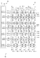
次に、本発明の第1実施形態に係る撮像装置100の回路構成を、図1及び図8を用いて説明する。図1及び図8は、本発明の第1実施形態に係る撮像装置100の回路構成を示す図である。
Next, the circuit configuration of the
撮像装置100は、画素ユニット配列10、駆動部20、及び読み出し部30を備える。
The
画素ユニット配列10は、後述の半導体基板SBにおける撮像領域IAに配される。駆動部20及び読み出し部30は、半導体基板SBにおける周辺領域PAに配される。周辺領域PAは、撮像領域IAの周辺に位置する領域である。
The
画素ユニット配列10では、複数の画素ユニットPU11〜PU33が水平方向及び垂直方向に配列されている。図1には、3行×3列の画素ユニットPU11〜PU33で構成された画素ユニット配列10が例示されている。各画素ユニットPU11〜PU33は、複数の画素が部分的に共通化された構成をしている。図1には、4画素が部分的に共通化された画素ユニットPU11〜PU33を例示している。すなわち、図1には、6行×6列の36画素の撮像領域を表しているが、実際の撮像領域には、数百万以上の画素が配される。
In the
駆動部20は、画素ユニット配列10を駆動する。駆動部20は、垂直走査回路107を含む。垂直走査回路107は、画素ユニット配列10を垂直方向に走査することにより、画素ユニット配列10における所定の画素行を選択し、選択された画素行の各画素を駆動する。
The
読み出し部30は、画素ユニット配列10における駆動部20により選択された画素行から信号を読み出す。読み出し部30は、ラインメモリLM、水平走査回路124、及び出力アンプ123を含む。ラインメモリLMは、選択された画素行から信号を読み出し一時的に保持する。水平走査回路124は、ラインメモリにより保持された画素行における各列の信号を順次に選択して出力アンプ123へ転送する。出力アンプ123は、転送された各列の信号から画像信号を生成して出力する。
The
ここで、ラインメモリLMは、主として、2つのノイズレベル保持容量CTNA、CTNBと2つの輝度レベル保持容量CTSA、CTSBとを、垂直信号線ごとに含む(図8参照)。各ノイズレベル保持容量CTNA、CTNBは、後述のノイズレベルの信号を保持する。各輝度レベル保持容量CTSA、CTSBは、後述の輝度レベルの信号を保持する。 Here, the line memory LM mainly includes two noise level holding capacitors CTNA and CTNB and two luminance level holding capacitors CTSA and CTSB for each vertical signal line (see FIG. 8). Each noise level holding capacitor CTNA, CTNB holds a signal of a noise level described later. Each luminance level holding capacitor CTSA, CTSB holds a luminance level signal described later.
次に、画素ユニット配列10の回路構成を説明する。以下では、画素ユニットPU12の構成を例示的に説明するが、他の画素ユニットPU11〜PU33の構成も、画素ユニットPU12の構成と同様である。
Next, the circuit configuration of the
画素ユニットPU12は、複数の光電変換部PD1−1〜PD1−4、電荷電圧変換部FD1、複数の転送トランジスタM1−1〜M1−4、増幅トランジスタM1−6、及びリセットトランジスタM1−7を含む。画素ユニットPU12では、4つの光電変換部PD1−1〜PD1−4と4つの転送トランジスタM1−1〜M1−4とに対して電荷電圧変換部FD1、リセットトランジスタM1−7、増幅トランジスタM1−6及び選択トランジスタM1−5が共通化されている。 The pixel unit PU12 includes a plurality of photoelectric conversion units PD1-1 to PD1-4, a charge / voltage conversion unit FD1, a plurality of transfer transistors M1-1 to M1-4, an amplification transistor M1-6, and a reset transistor M1-7. . In the pixel unit PU12, for the four photoelectric conversion units PD1-1 to PD1-4 and the four transfer transistors M1-1 to M1-4, the charge-voltage conversion unit FD1, the reset transistor M1-7, and the amplification transistor M1-6. The select transistor M1-5 is shared.
各光電変換部PD1−1〜PD1−4は、光に応じた電荷を発生させて蓄積する。光電変換部PD1−1〜PD1−4は、例えば、フォトダイオードである。 Each photoelectric conversion unit PD1-1 to PD1-4 generates and accumulates charges corresponding to light. The photoelectric conversion units PD1-1 to PD1-4 are, for example, photodiodes.
複数の転送トランジスタM1−1〜M1−4は、複数の光電変換部PD1−1〜PD1−4で発生した電荷を電荷電圧変換部FD1へ転送する。すなわち、転送トランジスタM1−1は、垂直走査回路107から転送制御線TX11_3経由でアクティブな制御信号がゲートに供給された際にオンすることにより、光電変換部PD1−1で発生した電荷を電荷電圧変換部FD1へ転送する。転送トランジスタM1−2は、垂直走査回路107から転送制御線TX12_4経由でアクティブな制御信号がゲートに供給された際にオンすることにより、光電変換部PD1−2で発生した電荷を電荷電圧変換部FD1へ転送する。転送トランジスタM1−3は、垂直走査回路107から転送制御線TX21_3経由でアクティブな制御信号がゲートに供給された際にオンすることにより、光電変換部PD1−3で発生した電荷を電荷電圧変換部FD1へ転送する。転送トランジスタM1−4は、垂直走査回路107から転送制御線TX22_4経由でアクティブな制御信号がゲートに供給された際にオンすることにより、光電変換部PD1−4で発生した電荷を電荷電圧変換部FD1へ転送する。
The plurality of transfer transistors M1-1 to M1-4 transfer the charges generated in the plurality of photoelectric conversion units PD1-1 to PD1-4 to the charge-voltage conversion unit FD1. In other words, the transfer transistor M1-1 is turned on when an active control signal is supplied from the
電荷電圧変換部FD1は、転送された電荷を電圧に変換する。電荷電圧変換部FD1は、例えば、フローティングディフュージョンである。 The charge-voltage converter FD1 converts the transferred charge into a voltage. The charge-voltage conversion unit FD1 is, for example, a floating diffusion.
リセットトランジスタM1−7は、電荷電圧変換部FD1をリセットする。すなわち、リセットトランジスタM1−7は、垂直走査回路107からリセット制御線RES1経由でアクティブな制御信号がゲートに供給された際にオンする。これにより、リセットトランジスタM1−7は、垂直電源線102−3からドレインに供給された電源電圧Vddに応じた電位に電荷電圧変換部FD1をリセットする。
The reset transistor M1-7 resets the charge-voltage conversion unit FD1. That is, the reset transistor M1-7 is turned on when an active control signal is supplied from the
増幅トランジスタM1−6は、電荷電圧変換部FD1の電圧に応じた信号を出力する。増幅トランジスタM1−6は、垂直電源線102−2からドレインに供給された電源電圧Vddに応じて垂直信号線103−2に接続された負荷電流源111とともにソースフォロワ動作を行う。これにより、増幅トランジスタM1−6は、電荷電圧変換部FD1の電圧に応じた信号を垂直信号線103−2へ出力する。増幅トランジスタM1−6は、リセットトランジスタM1−7により電荷電圧変換部FD1がリセットされた状態で、電荷電圧変換部FD1の電圧に応じたノイズレベルの信号を垂直信号線103−2へ出力する。増幅トランジスタM1−6は、光電変換部PD1−1〜PD1−4で発生した電荷が転送トランジスタM1−1〜M1−4により電荷電圧変換部FD1へ転送された状態で、電荷電圧変換部FD1の電圧に応じた輝度レベルの信号を垂直信号線103−2へ出力する。
The amplification transistor M1-6 outputs a signal corresponding to the voltage of the charge-voltage conversion unit FD1. The amplification transistor M1-6 performs a source follower operation together with the load
選択トランジスタM1−5は、画素ユニットPU12を選択状態/非選択状態にする。すなわち、選択トランジスタM1−5は、垂直走査回路107から選択制御線SEL1経由でアクティブな制御信号が供給された際にオンすることにより、画素ユニットPU12を選択状態/非選択状態にする。
The selection transistor M1-5 brings the pixel unit PU12 into a selected state / non-selected state. That is, the selection transistor M1-5 is turned on when an active control signal is supplied from the
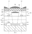
次に、撮像装置100の断面構成の概略を、図3を用いて説明する。
Next, an outline of a cross-sectional configuration of the
撮像装置100は、半導体基板SB及び多層配線構造MWSを備える。半導体基板SBは、撮像領域IAと周辺領域PAとを有する。多層配線構造MWSは、第1の絶縁層IL1、第1の配線層ML1、第2の絶縁層IL2、第2の配線層ML2、及び第3の絶縁層IL3を含む。
The
第1の絶縁層IL1は、半導体基板SBの上に配されている。第1の絶縁層IL1は、半導体基板SBと第1の配線層ML1とを絶縁する。 The first insulating layer IL1 is disposed on the semiconductor substrate SB. The first insulating layer IL1 insulates the semiconductor substrate SB from the first wiring layer ML1.
第1の配線層ML1は、複数の光電変換部のそれぞれに対する開口領域の水平方向の輪郭辺を規定するように、第1の絶縁層IL1の上すなわち半導体基板SBの上方に配されている。第1の配線層ML1は、例えば、光電変換部PD1−2に対する開口領域OAの水平方向の輪郭辺OAS1,OAS2を規定する(図5参照)。第1の配線層ML1は、例えば、アルミニウムを主成分とする金属又は金属間化合物で形成されている。 The first wiring layer ML1 is arranged on the first insulating layer IL1, that is, above the semiconductor substrate SB so as to define the horizontal contour side of the opening region for each of the plurality of photoelectric conversion units. The first wiring layer ML1 defines, for example, horizontal contour sides OAS1 and OAS2 of the opening region OA with respect to the photoelectric conversion unit PD1-2 (see FIG. 5). The first wiring layer ML1 is formed of, for example, a metal whose main component is aluminum or an intermetallic compound.
第2の絶縁層IL2は、第1の配線層ML1を覆うように第1の配線層ML1の上に配されている。第2の絶縁層IL2は、第1の配線層ML1と第2の配線層ML2とを絶縁する。 The second insulating layer IL2 is disposed on the first wiring layer ML1 so as to cover the first wiring layer ML1. The second insulating layer IL2 insulates the first wiring layer ML1 and the second wiring layer ML2.
第2の配線層ML2は、複数の光電変換部のそれぞれに対する開口領域の垂直方向の輪郭辺を規定するように、第2の絶縁層IL2の上すなわち第1の配線層ML1の上方に配されている。第2の配線層ML2は、例えば、光電変換部PD1−2に対する開口領域OAの垂直方向の輪郭辺OAS3,OAS4を規定する(図5参照)。第2の配線層ML2は、撮像領域IAにおける最上の配線層である。第2の配線層ML2は、例えば、アルミニウムを主成分とする金属又は金属間化合物で形成されている。 The second wiring layer ML2 is disposed on the second insulating layer IL2, that is, above the first wiring layer ML1, so as to define the vertical contour side of the opening region for each of the plurality of photoelectric conversion units. ing. The second wiring layer ML2 defines, for example, contour sides OAS3 and OAS4 in the vertical direction of the opening area OA with respect to the photoelectric conversion unit PD1-2 (see FIG. 5). The second wiring layer ML2 is the uppermost wiring layer in the imaging area IA. The second wiring layer ML2 is formed of, for example, a metal whose main component is aluminum or an intermetallic compound.
第3の絶縁層IL3は、第2の配線層ML2を覆うように第2の配線層ML2の上に配されている。第3の絶縁層IL3は、第2の配線層ML2と上層(層内レンズ、平坦化層など)とを絶縁する。 The third insulating layer IL3 is disposed on the second wiring layer ML2 so as to cover the second wiring layer ML2. The third insulating layer IL3 insulates the second wiring layer ML2 from the upper layer (intra-layer lens, planarization layer, etc.).
次に、画素ユニット配列10と駆動部20との間を水平方向に延びた各ライン(線)について、図1を用いて説明する。
Next, each line (line) extending in the horizontal direction between the
TX11_3、TX12_4、TX21_3、TX22_4、TX31_3、TX32_4、TX41_3、TX42_4は転送制御線である。RES1、RES2、RES3はリセット制御線である。SEL1、SEL2、SEL3は選択制御線である。これらのラインは、第1の配線層ML1(図3参照)として形成されている。 TX 1 1_3, TX 1 2_4, TX 2 1_3, TX 2 2_4, TX 3 1_3, TX 3 2_4, TX 4 1_3, and TX 4 2_4 are transfer control lines. RES1, RES2, and RES3 are reset control lines. SEL1, SEL2, and SEL3 are selection control lines. These lines are formed as the first wiring layer ML1 (see FIG. 3).
各転送制御線TX11_3〜TX42_4は、垂直方向に隣接する画素ユニットの間を延びており、垂直方向に隣接する転送トランジスタのゲートに対して共通の制御信号を供給するように構成されている。また、各転送制御線TX11_3〜TX42_4は、水平方向に隣接する画素ユニットにおける対応した転送トランジスタのゲートに対して共通の制御信号を供給するように構成されている。 Each transfer control line TX 1 1_3 to TX 4 2_4 extends between adjacent pixel units in the vertical direction, and is configured to supply a common control signal to the gates of the transfer transistors adjacent in the vertical direction. ing. The transfer control lines TX 1 1_3 to TX 4 2_4 are configured to supply a common control signal to the gates of the corresponding transfer transistors in the pixel units adjacent in the horizontal direction.
各リセット制御線RES1〜RES3は、垂直方向に隣接する画素ユニットの間を延びており、垂直方向に隣接するリセットトランジスタのゲートに対して共通の制御信号を供給するように構成されている。また、各リセット制御線RES1〜RES3は、水平方向に隣接する画素ユニットにおける対応したリセットトランジスタのゲートに対して共通の制御信号を供給するように構成されている。 Each reset control line RES1 to RES3 extends between adjacent pixel units in the vertical direction, and is configured to supply a common control signal to the gates of the reset transistors adjacent in the vertical direction. The reset control lines RES1 to RES3 are configured to supply a common control signal to the gates of the corresponding reset transistors in the pixel units adjacent in the horizontal direction.
各選択制御線SEL1〜SEL3は、垂直方向に隣接する画素ユニットの間を延びており、垂直方向に隣接する選択トランジスタのゲートに対して共通の制御信号を供給するように構成されている。また、各選択制御線RES1〜RES3は、水平方向に隣接する画素ユニットにおける対応した選択トランジスタのゲートに対して共通の制御信号を供給するように構成されている。 Each selection control line SEL1 to SEL3 extends between adjacent pixel units in the vertical direction, and is configured to supply a common control signal to the gates of the selection transistors adjacent in the vertical direction. The selection control lines RES1 to RES3 are configured to supply a common control signal to the gates of the corresponding selection transistors in the pixel units adjacent in the horizontal direction.
このように、第1の配線層ML1におけるラインが共通化されているので、第1の配線層ML1におけるラインの数が低減されている。 Thus, since the lines in the first wiring layer ML1 are shared, the number of lines in the first wiring layer ML1 is reduced.
次に、画素ユニット配列10と読み出し部30との間を垂直方向に延びた各ライン(線)について、図1を用いて説明する。
Next, each line (line) extending in the vertical direction between the
102−1,102−2,102−3は垂直電源線である。103−1,103−2,103−3は垂直信号線である。垂直電源線102−1〜102−3と垂直信号線103−1〜103−3とは、水平方向へ交互に繰り返し配列されている。これらのラインは、第2の配線層ML2(図3参照)として形成されている。 Reference numerals 102-1, 102-2, and 102-3 denote vertical power supply lines. Reference numerals 103-1, 103-2, and 103-3 denote vertical signal lines. The vertical power supply lines 102-1 to 102-3 and the vertical signal lines 103-1 to 103-3 are alternately and repeatedly arranged in the horizontal direction. These lines are formed as the second wiring layer ML2 (see FIG. 3).
各垂直電源線102−1〜102−3は、画素ユニットの増幅トランジスタ又はリセットトランジスタへ電源を供給するように、水平方向に隣接する2つの画素ユニットの間を垂直方向に延びている。各垂直電源線102−1〜102−3は、第1の側(図1における左側)の画素ユニットにおけるリセットトランジスタへ電源電圧を供給し、第2の側(図1における右側)の画素ユニットにおける増幅トランジスタへ電源電圧を供給する。すなわち、各垂直電源線102−1〜102−3は、第1の側に配されたリセットトランジスタと第2の側に配された増幅トランジスタとに対して共通の電源電圧を供給するように構成されている。これにより、画素ユニットでは、水平方向の第1の側に隣接する画素ユニットとの間を延びた第1の垂直電源線から増幅トランジスタへ電源電圧が供給される。また、画素ユニットでは、水平方向の第2の側に隣接する画素ユニットとの間を延びた第2の垂直電源線からリセットトランジスタへ電源電圧が供給される。 Each of the vertical power supply lines 102-1 to 102-3 extends in the vertical direction between two pixel units adjacent in the horizontal direction so as to supply power to the amplification transistor or the reset transistor of the pixel unit. Each vertical power supply line 102-1 to 102-3 supplies a power supply voltage to the reset transistor in the pixel unit on the first side (left side in FIG. 1), and in the pixel unit on the second side (right side in FIG. 1). A power supply voltage is supplied to the amplification transistor. That is, each vertical power supply line 102-1 to 102-3 is configured to supply a common power supply voltage to the reset transistor arranged on the first side and the amplification transistor arranged on the second side. Has been. Thereby, in the pixel unit, the power supply voltage is supplied to the amplification transistor from the first vertical power supply line extending between the pixel unit adjacent to the first side in the horizontal direction. In the pixel unit, the power supply voltage is supplied to the reset transistor from the second vertical power supply line extending between the pixel unit adjacent to the second side in the horizontal direction.
各垂直信号線103−1〜103−3は、画素ユニットの増幅トランジスタから出力された信号を伝達するように、画素ユニットにおける複数の光電変換部の間を垂直方向に延びている。各垂直信号線103−1〜103−3は、画素ユニットにおける複数の光電変換部に対して共通の信号線となっているとともに、画素ユニット配列における垂直方向に並んだ画素ユニットに対して共通の信号線となっている。 Each of the vertical signal lines 103-1 to 103-3 extends in the vertical direction between a plurality of photoelectric conversion units in the pixel unit so as to transmit a signal output from the amplification transistor of the pixel unit. Each of the vertical signal lines 103-1 to 103-3 is a common signal line for a plurality of photoelectric conversion units in the pixel unit, and is common to the pixel units arranged in the vertical direction in the pixel unit array. It is a signal line.
このように、第2の配線層ML2におけるラインが共通化されるとともに均等に(等間隔に)配されているので、第2の配線層ML2におけるラインの数が低減されている。すなわち、多層配線構造MWSでは、撮像領域IAにおける最上の配線層(図3参照)である第2の配線層ML2におけるラインの数が低減されている。これにより、光電変換部の開口領域(例えば、図5に示す開口領域OA)の幅を広く確保することができるので、開口領域を規定する配線による光の回折を抑制することができる。これにより、開口領域を規定する配線による回折に起因した光学的混色を低減することができる。 As described above, since the lines in the second wiring layer ML2 are made common and are evenly arranged (at equal intervals), the number of lines in the second wiring layer ML2 is reduced. That is, in the multilayer wiring structure MWS, the number of lines in the second wiring layer ML2 that is the uppermost wiring layer (see FIG. 3) in the imaging region IA is reduced. Thereby, since the width | variety of the opening area | region (for example, opening area OA shown in FIG. 5) of a photoelectric conversion part can be ensured widely, the diffraction of the light by the wiring which prescribes | regulates an opening area | region can be suppressed. Thereby, the optical color mixture resulting from the diffraction by the wiring which defines the opening region can be reduced.
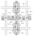
次に、画素ユニットPU12及びその周辺のレイアウト構成を、図2を用いて説明する。図2は、画素ユニットPU12及びその周辺において第2の配線層ML2、スルーホール115、第1の配線層ML1(図3参照)を取り去って見た場合の平面図である。 Next, the layout configuration of the pixel unit PU12 and its periphery will be described with reference to FIG. FIG. 2 is a plan view of the pixel unit PU12 and its periphery when the second wiring layer ML2, the through hole 115, and the first wiring layer ML1 (see FIG. 3) are removed.
図2において、149−1、149−2、149−3はシェアードコンタクトである。150−1、150−2は多結晶シリコン領域である。116−1、116−2、116−3、116−4、116−5はコンタクトである。144−1はアクティブ領域とフィールド酸化領域の境界である。142−1、142−2、142−3はフィールド酸化領域である。145−1、145−2、145−3、145−4はアクティブ領域である。 In FIG. 2, 149-1, 149-2, and 149-3 are shared contacts. Reference numerals 150-1 and 150-2 denote polycrystalline silicon regions. Reference numerals 116-1, 116-2, 116-3, 116-4, and 116-5 are contacts. 144-1 is a boundary between the active region and the field oxidation region. Reference numerals 142-1, 142-2, and 142-3 are field oxidation regions. Reference numerals 145-1, 145-2, 145-3, and 145-4 denote active areas.
アクティブ領域145−1は、それぞれ、光電変換部PD1−1〜PD1−4が形成された領域である。アクティブ領域145−2は、MOSトランジスタ(例えば、選択トランジスタM1−5、増幅トランジスタM1−6、リセットトランジスタM1−7)が形成された領域である。アクティブ領域145−3は、電荷電圧変換部FD1が形成された領域である。電荷電圧変換部FD1は、不純物を含む半導体領域として形成されている。フィールド酸化領域142は、アクティブ領域145の素子分離を行うように配されている。例えば、アクティブ領域とフィールド酸化領域との境界144−1の左側には、光電変換部PD1−2を含むアクティブ領域145−1がある。境界144−1の右側にはフィールド酸化領域142−1がある。
The active region 145-1 is a region where the photoelectric conversion units PD1-1 to PD1-4 are formed, respectively. The active region 145-2 is a region where MOS transistors (for example, the selection transistor M1-5, the amplification transistor M1-6, and the reset transistor M1-7) are formed. The active region 145-3 is a region where the charge / voltage conversion unit FD1 is formed. The charge-voltage conversion unit FD1 is formed as a semiconductor region containing impurities. The
次に、画素ユニットPU12及びその周辺の断面構成を、図3を用いて説明する。図3は、図2の平面図におけるB−B’線で切った断面図である。 Next, a cross-sectional configuration of the pixel unit PU12 and its periphery will be described with reference to FIG. 3 is a cross-sectional view taken along line B-B ′ in the plan view of FIG. 2.
図3において、118の網掛けパターンはp型領域、119の網掛けパターンはn型領域を表す。また、143−1、143−2はソース領域、147、148は共通ドレイン領域、113−7、113−8、113−9は第1の配線層におけるパターン、115−1、115−2、115−3はスルーホールである。他の符号は、図1及び図2と同様である。
In FIG. 3, the hatched
コンタクト116−3は、第1の配線層におけるパターン113−7と、リセットトランジスタM0−7(図1参照)及び選択トランジスタM1−5の共通ドレイン領域147とを電気的に接続している。
The contact 116-3 electrically connects the pattern 113-7 in the first wiring layer to the
コンタクト116−4は、第1の配線層におけるパターン113−8と、増幅トランジスタM1−6のソース領域143−1とを電気的に接続している。 The contact 116-4 electrically connects the pattern 113-8 in the first wiring layer and the source region 143-1 of the amplification transistor M1-6.
コンタクト116−5は、第1の配線層におけるパターン113−9と、リセットトランジスタM1−7及び選択トランジスタM4−5の共通ドレイン領域147とを電気的に接続している。
The contact 116-5 electrically connects the pattern 113-9 in the first wiring layer and the
スルーホール115−1は、第1の配線層におけるパターン113−7と第2の配線層におけるラインからなる垂直電源線102−2とを電気的に接続している。スルーホール115−2は、第1の配線層におけるパターン113−8と第2の配線層におけるラインからなる垂直信号線103−2とを電気的に接続している。スルーホール115−3は、第1の配線層におけるパターン113−9と第2の配線層におけるラインからなる垂直電源線102−3とを電気的に接続している。 The through hole 115-1 electrically connects the pattern 113-7 in the first wiring layer and the vertical power supply line 102-2 made up of lines in the second wiring layer. The through hole 115-2 is electrically connected to the pattern 113-8 in the first wiring layer and the vertical signal line 103-2 including the lines in the second wiring layer. The through hole 115-3 electrically connects the pattern 113-9 in the first wiring layer and the vertical power supply line 102-3 composed of lines in the second wiring layer.
すなわち、図2及び図3に示すように、増幅トランジスタとリセットトランジスタと選択トランジスタとのチャンネル長の方向は、垂直信号線と垂直電源線とが延びた方向に交差する方向、すなわち水平方向に沿っている。このように配置した結果、電源電圧Vddが、共通ドレイン領域147と148とへ、それぞれ別の垂直電源線102と102−3から供給される。この電源電圧Vddは、1〜5Vが望ましく、さらに望ましくは、2.5〜3.3Vである。
That is, as shown in FIGS. 2 and 3, the channel length directions of the amplification transistor, the reset transistor, and the selection transistor are along the direction intersecting with the direction in which the vertical signal line and the vertical power supply line extend, that is, the horizontal direction. ing. As a result of this arrangement, the power supply voltage Vdd is supplied to the
以上のように配置することによって、増幅トランジスタM1−6のソース領域143−1が、垂直電源線102−2と垂直電源線102−3とのちょうど中間付近の下に配される。このため、図3の断面図で示されるように、コンタクト116−4、第1の配線層におけるパターン113−8、スルーホール115−2介してソース領域143−1に接続される第2の配線層における垂直信号線103を、画素境界137−2上に配置できる。これにより、画素の1列につき垂直方向の配線が1本になるようにレイアウトすることができ、第2の配線層における垂直電源線と垂直信号線とを等間隔となるようにレイアウトすることができる。このことは、後で詳述するが光の回折が起こってしまう縮小化画素では、大きな効果をもたらす。
With the arrangement as described above, the source region 143-1 of the amplification transistor M1-6 is arranged just below the middle between the vertical power supply line 102-2 and the vertical power supply line 102-3. Therefore, as shown in the sectional view of FIG. 3, the second wiring connected to the source region 143-1 through the contact 116-4, the pattern 113-8 in the first wiring layer, and the through hole 115-2. The
図3の断面図で示すとおり、シェアードコンタクト149−2は、リセットトランジスタM1−7のソース領域143−2と多結晶シリコン領域150−2とを電気的に接続している。図2の平面図で示されるように、多結晶シリコン領域150−2は、多結晶シリコン領域からなる増幅トランジスタM1−6のゲート電極に多結晶シリコン配線で電気的に接続されている。 As shown in the sectional view of FIG. 3, the shared contact 149-2 electrically connects the source region 143-2 of the reset transistor M1-7 and the polycrystalline silicon region 150-2. As shown in the plan view of FIG. 2, the polycrystalline silicon region 150-2 is electrically connected to the gate electrode of the amplification transistor M1-6 made of the polycrystalline silicon region by a polycrystalline silicon wiring.
シェアードコンタクト149−1は、多結晶シリコン領域150−2と電荷電圧変換部FD1とを電気的に接続している。 Shared contact 149-1 electrically connects polycrystalline silicon region 150-2 and charge-voltage conversion unit FD1.
多結晶シリコン領域150−1は、転送トランジスタM1−3のゲート電極になっており、コンタクト116−2を介して第1の配線層におけるライン113−5(図2及び図4参照)と接続されている。 The polycrystalline silicon region 150-1 is a gate electrode of the transfer transistor M1-3, and is connected to the line 113-5 (see FIGS. 2 and 4) in the first wiring layer through the contact 116-2. ing.
本実施形態において、電気的に接続された電荷電圧変換部(フローティングディフュージョン)はひとつの電荷電圧変換部とみなす。つまり、図2において、アクティブ領域145−3とアクティブ領域145−4とは、シェアードコンタクト149−3、多結晶シリコン領域142−3、シェアードコンタクト149−1によって接続されているので、1つの電荷電圧変換部FD1とみなす。 In the present embodiment, an electrically connected charge / voltage converter (floating diffusion) is regarded as one charge / voltage converter. That is, in FIG. 2, since the active region 145-3 and the active region 145-4 are connected by the shared contact 149-3, the polycrystalline silicon region 142-3, and the shared contact 149-1, one charge voltage Considered as the conversion unit FD1.
図4は、図2の平面図に対して、スルーホール115及び第1の配線層ML1をさらに配置した場合の平面図である。 FIG. 4 is a plan view in the case where the through hole 115 and the first wiring layer ML1 are further arranged with respect to the plan view of FIG.
図4において、転送制御線TX11_3、TX12_4、TX21_3、TX22_4は、それぞれ、第1の配線層ML1におけるライン113−1、113−2、113−5、113−6から構成される。 In FIG. 4, transfer control lines TX 1 1_3, TX 1 2_4, TX 2 1_3, TX 2 2_4 are respectively connected to lines 113-1, 113-2, 113-5, and 113-6 in the first wiring layer ML1. Composed.
選択制御線SEL1、リセット制御線RES1は、それぞれ、第1の配線層ML1におけるライン113−3、113−4から構成される。 The selection control line SEL1 and the reset control line RES1 are composed of lines 113-3 and 113-4 in the first wiring layer ML1, respectively.
スルーホール115−1、115−2、115−3の下部には、第1の配線層ML1における島状のパターン113−7、113−8、113−9がある。 Below the through holes 115-1, 115-2, and 115-3, there are island-like patterns 113-7, 113-8, and 113-9 in the first wiring layer ML1.
次に、画素ユニットにおける電荷の転送を、光電変換部PD1−3に注目して説明する。 Next, charge transfer in the pixel unit will be described by paying attention to the photoelectric conversion units PD1-3.
光電変換部PD1−3における蓄積される電荷の数は、光電変換部PD1−3の受光面が照射された光量に応じて増える。転送トランジスタM1−3は、転送制御線TX21_3を介してアクティブな制御信号(パルス)がゲートに入力されたとき、オンする。これにより、光電変換部PD1−3で蓄積された電荷が、電荷電圧変換部FD1に完全転送される。電荷電圧変換部FD1は、寄生容量を有しているので、光電変換部PD1−3から転送された電荷の数に応じて、その電位が変化する。 The number of charges accumulated in the photoelectric conversion units PD1-3 increases in accordance with the amount of light irradiated on the light receiving surface of the photoelectric conversion units PD1-3. The transfer transistor M1-3 is turned on when an active control signal (pulse) is input to the gate via the transfer control line TX 2 1_3. As a result, the charges accumulated in the photoelectric conversion units PD1-3 are completely transferred to the charge-voltage conversion unit FD1. Since the charge-voltage conversion unit FD1 has a parasitic capacitance, the potential changes according to the number of charges transferred from the photoelectric conversion units PD1-3.
図5は、図4の平面図に対して、第2の配線層ML2をさらに配置した場合の平面図である。 FIG. 5 is a plan view when a second wiring layer ML2 is further arranged with respect to the plan view of FIG.
図5において、垂直電源線102−2、垂直信号線103−2、垂直電源線102−3は、第2の配線層ML2におけるラインである。 In FIG. 5, a vertical power supply line 102-2, a vertical signal line 103-2, and a vertical power supply line 102-3 are lines in the second wiring layer ML2.
垂直電源線102−2は、光電変換部PD1−1、PD1−3、PD2−1の左側に配置される。垂直電源線102−3は、光電変換部PD1−2、PD1−4、PD2−2の右側に垂直方向に配置される。また、垂直信号線103−2は、光電変換部PD1−1、PD1−3、PD2−1の右側で、光電変換部PD1−2、PD1−4、PD2−2の左側、つまり両者の間に配置される。 The vertical power supply line 102-2 is disposed on the left side of the photoelectric conversion units PD1-1, PD1-3, and PD2-1. The vertical power supply line 102-3 is arranged in the vertical direction on the right side of the photoelectric conversion units PD1-2, PD1-4, and PD2-2. The vertical signal line 103-2 is on the right side of the photoelectric conversion units PD1-1, PD1-3, and PD2-1 and on the left side of the photoelectric conversion units PD1-2, PD1-4, and PD2-2, that is, between the two. Be placed.
本実施形態では、撮像装置は、例えば単板式のカラーCMOSエリアセンサであるため、カラーフィルタを第2の配線層におけるラインの上層に配置している。このカラーフィルタについて説明する。 In the present embodiment, since the imaging device is, for example, a single-plate color CMOS area sensor, the color filter is disposed above the line in the second wiring layer. This color filter will be described.
図6は、図5の平面図に対してカラーフィルタを被せた場合の平面図である。 FIG. 6 is a plan view when a color filter is put on the plan view of FIG.
図6において、132は、ブルー(B)の光を選択的に透過するカラーフィルタカラーフィルタである。133は、レッド(R)の光を選択的に透過するカラーフィルタである。134、135は、グリーン(Gr,Gb)の光を選択的に透過するカラーフィルタである。
In FIG. 6,
図6の示されるように、カラーフィルタの配置は、ベイヤー配列を形成している。このベイヤー配列は、カラー画像の分解能を高める上で役立っており、ほとんどの単板型エリアセンサで採用されている。ここで、グリーンカラーフィルタ134が配された画素は、水平方向にブルー(B)の画素が隣接しているという意味でGb画素と呼ばれ、グリーンカラーフィルタ135が配された画素は、水平方向にレッド(R)の画素が隣接しているという意味でGr画素と呼ぶ。
As shown in FIG. 6, the arrangement of the color filters forms a Bayer array. This Bayer arrangement is useful for increasing the resolution of color images, and is used in most single-plate area sensors. Here, the pixel on which the
ここで、図1の等価回路図と、図2、図4、図5で示した撮像領域の平面図で示したように、本実施形態の画素の繰り返し周期は、2行2列の4画素周期である。図6のようにベイヤー配列も2行2列の4画素周期であるため、本実施形態の画素はベイヤー配列に適している。画素ユニット配列における各画素ユニットは、複数の光電変換部に対応した複数のカラーフィルタをさらに含んでいる。各カラーフィルタは、光電変換部に所定の色(波長)の光が入射するように、その所定の色(波長)の光を選択的に透過する。 Here, as shown in the equivalent circuit diagram of FIG. 1 and the plan view of the imaging region shown in FIGS. 2, 4, and 5, the repetition cycle of the pixel of this embodiment is 4 pixels of 2 rows and 2 columns. It is a period. As shown in FIG. 6, the Bayer array has a 4-pixel cycle of 2 rows and 2 columns, and thus the pixels of this embodiment are suitable for the Bayer array. Each pixel unit in the pixel unit array further includes a plurality of color filters corresponding to the plurality of photoelectric conversion units. Each color filter selectively transmits light of a predetermined color (wavelength) so that light of a predetermined color (wavelength) enters the photoelectric conversion unit.
具体的には、ブルーカラーフィルタ132が配された画素は、撮像領域全体にわたり、画素ユニット内における相対的な位置が同じになる、すなわち同じレイアウトになる。レッドカラーフィルタ133が配された画素は、撮像領域全体にわたり必ず同じレイアウトである。また、Gb画素も撮像領域全体にわたり必ず同じレイアウトであり、Gr画素も撮像領域全体にわたり必ず同じレイアウトである。このため、隣接する同色の画素間で感度差を招くことを抑制できる。
Specifically, the pixels provided with the
本実施形態では、光学的混色を、隣接画素間の光の混じり合いと定義している。本実施形態をモノクロのエリアセンサ、三板式などのエリアセンサに適用しても、隣接する画素間の光の混じり合いを防ぐことができるので、センサの実質解像度を高めるという効果がある。 In this embodiment, the optical color mixture is defined as a light mixture between adjacent pixels. Even if the present embodiment is applied to a monochrome area sensor, a three-plate type area sensor, or the like, it is possible to prevent light from being mixed between adjacent pixels, so that there is an effect of increasing the substantial resolution of the sensor.
図7は、図5の平面図のAA’線で切った場合の断面図である。 7 is a cross-sectional view taken along the line AA 'in the plan view of FIG.
図7において、129はシリコン基板と層間絶縁膜の境界、137は、画素境界、138は、オンチップマイクロレンズ、139は、光束、140は、平坦化樹脂層、141は層内レンズを表す。他の符号は、図1から図6と同様である。
In FIG. 7,
光電変換部PD1−2の上部の右側には、第2の配線層ML2におけるラインとして垂直電源線102−3の1本のみのが配されている。光電変換部PD1−2の上部の左側には、第2の配線層ML2におけるラインとして垂直信号線103−2の1本のみが配されている。このため、撮像装置全体では、画素1列あたり1本の第2の配線層におけるラインが配されているということになる。この結果、従来の画素1列あたり1.5本以上の第2の配線層ML2におけるラインの構造に比べて、回折による光束139の拡がり抑えられ、光学的混色が小さくなる。 On the right side of the upper part of the photoelectric conversion unit PD1-2, only one vertical power supply line 102-3 is arranged as a line in the second wiring layer ML2. On the left side of the upper portion of the photoelectric conversion unit PD1-2, only one vertical signal line 103-2 is arranged as a line in the second wiring layer ML2. For this reason, in the entire imaging apparatus, one line in the second wiring layer is arranged per pixel column. As a result, compared to the conventional line structure in the second wiring layer ML2 of 1.5 or more per pixel column, the spread of the light beam 139 due to diffraction is suppressed, and optical color mixing is reduced.
また、第1実施形態により、光電変換部の受光面の法線方向から透視した場合に、第2の配線層ML2におけるライン102−2、103−2、102−3の光電変換部の受光面上への張り出しが、従来に比べて小さくなる。このため、オンチップマイクロレンズ138や層内レンズ141の回折限界により集め切れなかった光のけられが低減できる。この結果、感度も高まる。
In addition, according to the first embodiment, when viewed from the normal direction of the light receiving surface of the photoelectric conversion unit, the light receiving surfaces of the photoelectric conversion units of the lines 102-2, 103-2, and 102-3 in the second wiring layer ML2 The overhang is smaller than before. For this reason, the vignetting of light that cannot be collected due to the diffraction limit of the on-
図3及び図7の断面図や図5の平面図に示すように、光電変換部PD1−2の列の右側の垂直電源線102−3と、左側の垂直信号線103−2は、画素境界137に配置される。また、図5の平面図に示すように光電変換部PD1−1の列の左側の垂直電源線102−2は画素境界に配置される。この構成により、光電変換部PD1−1の列とPD1−2の列とのバランスをとることができ、両画素のフォトダイオードへの入射光量を等しくすることが容易である。 As shown in the cross-sectional views of FIGS. 3 and 7 and the plan view of FIG. 5, the vertical power supply line 102-3 on the right side of the column of the photoelectric conversion unit PD1-2 and the vertical signal line 103-2 on the left side are pixel boundaries. 137. Further, as shown in the plan view of FIG. 5, the vertical power supply line 102-2 on the left side of the column of the photoelectric conversion units PD1-1 is arranged at the pixel boundary. With this configuration, it is possible to balance the columns of the photoelectric conversion units PD1-1 and the columns of PD1-2, and it is easy to make the amounts of incident light to the photodiodes of both pixels equal.
また、第1実施形態では、図3及び図7の断面図で示すように、撮像領域IAの配線層は、ライン113を含む第1の配線層ML1と、垂直電源線102−2、102−3、垂直信号線103−2を含む第2の配線層ML2との2層のみである。つまり、撮像領域IA内の配線層は、第1の配線層ML1と第2の配線層ML2とのみである。この構造は、縮小画素の光の回折を低減することに適している。 In the first embodiment, as shown in the cross-sectional views of FIGS. 3 and 7, the wiring layer of the imaging region IA includes the first wiring layer ML1 including the line 113 and the vertical power supply lines 102-2 and 102-. 3. Only two layers including the second wiring layer ML2 including the vertical signal line 103-2. That is, the wiring layers in the imaging area IA are only the first wiring layer ML1 and the second wiring layer ML2. This structure is suitable for reducing the light diffraction of the reduced pixel.
第1実施形態における撮像装置の駆動方法について、周辺領域を示す等価回路図である図8と垂直走査回路と撮像領域の等価回路図である図1で説明する。 The driving method of the image pickup apparatus according to the first embodiment will be described with reference to FIG. 8 which is an equivalent circuit diagram showing a peripheral region and FIG. 1 which is an equivalent circuit diagram of a vertical scanning circuit and an image pickup region.
図8に示す読み出し部30おいて、111は負荷電流源、121は輝度レベル用水平信号線、122はノイズレベル用水平信号線、123は出力アンプ、124は水平走査回路、125は外部信号端子を表す。151、152、153、154は信号サンプリング線を表し、φPTN_A、φPTS_A、φPTN_B、φPTS_Bは、それぞれ信号サンプリング線の電圧パルスを表す。
8, 111 is a load current source, 121 is a luminance level horizontal signal line, 122 is a noise level horizontal signal line, 123 is an output amplifier, 124 is a horizontal scanning circuit, and 125 is an external signal terminal. Represents.
また、M11〜M14はサンプリングトランジスタ、M15〜M18は水平出力トランジスタである。また、CTNA、CTNBはノイズレベル保持容量、CTSA、CTSBは輝度レベル保持容量である。155〜160は、水平走査回路124の出力線である。
M11 to M14 are sampling transistors, and M15 to M18 are horizontal output transistors. CTNA and CTNB are noise level holding capacitors, and CTSA and CTSB are luminance level holding capacitors. 155 to 160 are output lines of the
図9のタイミングチャートでタイミングについて説明する。図9は、第1実施形態における撮像装置の駆動方法を示すタイミングチャートである。以下では、垂直走査回路107から画素ユニット配列10又は読み出し部30へ供給される制御信号について説明する。
Timing will be described with reference to the timing chart of FIG. FIG. 9 is a timing chart illustrating a method for driving the imaging apparatus according to the first embodiment. Hereinafter, control signals supplied from the
まずタイミングt1で、φRes1とφRes2と(図1参照)をアクティブにする。これにより、第1行の画素ユニットPU11〜PU13及び第2行の画素ユニットPU21〜PU23において、リセットトランジスタがオンし、電荷電圧変換部が電源電位Vddに同時にリセットされる。 First, at timing t1, φRes1 and φRes2 (see FIG. 1) are activated. Thereby, in the pixel units PU11 to PU13 in the first row and the pixel units PU21 to PU23 in the second row, the reset transistors are turned on, and the charge-voltage converter is simultaneously reset to the power supply potential Vdd.
つぎにタイミングt2で、パルスφSEL1とφPTN_Aとをアクティブにする。これにより、第1行の画素ユニットPU11〜PU13が選択状態になるとともにノイズレベルの信号を垂直信号線103−1〜103−3へ出力する。サンプリングトランジスタM11がオンするので、垂直信号線103−1〜103−3へ出力された各列のノイズレベルの信号は、各列のノイズレベル保持容量CTNAに書き込まれる。 Next, at timing t2, the pulses φSEL1 and φPTN_A are activated. As a result, the pixel units PU11 to PU13 in the first row are selected, and noise level signals are output to the vertical signal lines 103-1 to 103-3. Since the sampling transistor M11 is turned on, the signal of the noise level of each column output to the vertical signal lines 103-1 to 103-3 is written to the noise level holding capacitor CTNA of each column.
つぎにタイミングt3で、φSEL2とφPTN_Bとをアクティブにする。これにより、第2行の画素ユニットPU21〜PU23が選択状態になるとともにノイズレベルの信号を垂直信号線103−1〜103−3へ出力する。サンプリングトランジスタM13がオンするので、垂直信号線103−1〜103−3へ出力された各列のノイズレベルの信号は、各列のノイズレベル保持容量CTNBに書き込まれる。 Next, at timing t3, φSEL2 and φPTN_B are activated. As a result, the pixel units PU21 to PU23 in the second row are selected, and noise level signals are output to the vertical signal lines 103-1 to 103-3. Since the sampling transistor M13 is turned on, the signal of the noise level of each column output to the vertical signal lines 103-1 to 103-3 is written to the noise level holding capacitor CTNB of each column.
つぎにタイミングt4で、φTX21_3をアクティブにする。光照射による光電変換部PD1−3に蓄積された電荷が電荷電圧変換部FD1に転送される。同時に、光照射による光電変換部PD2−1に蓄積された電荷が電荷電圧変換部FD2に転送される。 Next, at time t4, φTX 2 1_3 is activated. The charges accumulated in the photoelectric conversion units PD1-3 due to light irradiation are transferred to the charge-voltage conversion unit FD1. At the same time, the charge accumulated in the photoelectric conversion unit PD2-1 due to light irradiation is transferred to the charge-voltage conversion unit FD2.
つぎに、タイミングt5で、φSEL1とφPTS_Aとをアクティブにする。これにより、第1行の画素ユニットPU11〜PU13が選択状態になるとともに輝度レベルの信号を垂直信号線103−1〜103−3へ出力する。サンプリングトランジスタM12がオンするので、垂直信号線103−1〜103−3へ出力された各列の輝度レベルの信号は、各列の輝度レベル保持容量CTSAに書き込まれる。 Next, at time t5, φSEL1 and φPTS_A are activated. Thereby, the pixel units PU11 to PU13 in the first row are selected, and luminance level signals are output to the vertical signal lines 103-1 to 103-3. Since the sampling transistor M12 is turned on, the signal of the luminance level of each column output to the vertical signal lines 103-1 to 103-3 is written in the luminance level holding capacitor CTSA of each column.
つぎに、タイミングt6で、φSEL2とφPTN_Bとをアクティブにする。これにより、第2行の画素ユニットPU21〜PU23が選択状態になるとともに輝度レベルの信号を垂直信号線103−1〜103−3へ出力する。サンプリングトランジスタM14がオンするので、垂直信号線103−1〜103−3へ出力された各列の輝度レベルの信号は、各列の輝度レベル保持容量CTSBに書き込まれる。 Next, at time t6, φSEL2 and φPTN_B are activated. Accordingly, the pixel units PU21 to PU23 in the second row are selected, and luminance level signals are output to the vertical signal lines 103-1 to 103-3. Since the sampling transistor M14 is turned on, the signal of the luminance level of each column output to the vertical signal lines 103-1 to 103-3 is written in the luminance level holding capacitor CTSB of each column.
つぎに、タイミングt7以降で、水平走査回路124がその出力線155〜160に左から順に出力パルスを送り、水平出力トランジスタM15〜M18が順次オンする。ただし、M15とM16とがオンするタイミングは同時であり、M17とM18とがオンするタイミングも同時である。
Next, after timing t7, the
M15及びM16がオンするタイミングではノイズレベル保持容量CTNAに書き込まれたノイズレベル及び輝度レベル保持容量CTSAに書き込まれた輝度レベルがそれぞれノイズレベル用水平信号線122及び輝度レベル用水平信号線121へ出力される。
At the timing when M15 and M16 are turned on, the noise level written in the noise level holding capacitor CTNA and the luminance level written in the luminance level holding capacitor CTSA are output to the noise level
M17及びM18がオンするタイミングではノイズレベル保持容量CTNBに書き込まれたノイズレベル及び輝度レベル保持容量CTSBに書き込まれた輝度レベルがそれぞれノイズレベル用水平信号線122及び輝度レベル用水平信号線121へ出力される。
At the timing when M17 and M18 are turned on, the noise level written in the noise level holding capacitor CTNB and the luminance level written in the luminance level holding capacitor CTSB are output to the noise level
出力アンプ123は、輝度レベル用水平信号線121から入った輝度レベルから、ノイズレベル用水平信号線122からのノイズレベルを引き算し、画像信号を生成して外部信号端子125から出力する。
The
このようにして、光電変換部PD1−3を含む行とPD2−1を含む行とにおける半分の画素の走査が終わる。つまり、4画素共有の1画素ユニットPU12における左半分の光電変換部(画素)の走査が終わる。 In this way, scanning of half of the pixels in the row including the photoelectric conversion units PD1-3 and the row including the PD2-1 is completed. That is, the scanning of the left half photoelectric conversion unit (pixel) in the one-pixel unit PU12 sharing four pixels is completed.
タイミングt8〜タイミングt10における動作は、タイミングt1〜t3における動作と同様である。 The operation from timing t8 to timing t10 is the same as the operation from timing t1 to t3.
タイミングt11で、φTX22_4をアクティブにする。光照射による光電変換部PD1−4に蓄積された電荷が電荷電圧変換部FD1に転送される。同時に、光照射による光電変換部PD2−2に蓄積された電荷が電荷電圧変換部FD2に転送される。 At timing t11, φTX 2 2_4 is activated. The charges accumulated in the photoelectric conversion units PD1-4 due to light irradiation are transferred to the charge-voltage conversion unit FD1. At the same time, the charge accumulated in the photoelectric conversion unit PD2-2 due to light irradiation is transferred to the charge-voltage conversion unit FD2.
タイミングt12〜t14における動作は、タイミングt5〜t7における動作と同様である。 The operation at timings t12 to t14 is the same as the operation at timings t5 to t7.
このようにして、光電変換部PD1−3を含む行とPD2−1を含む行とにおける残り半分の画素の走査が終わる。つまり、4画素共有の1画素ユニットPU12における右半分の光電変換部(画素)の走査が終わる。 In this way, scanning of the remaining half of the pixels in the row including the photoelectric conversion units PD1-3 and the row including PD2-1 is completed. That is, the scanning of the photoelectric conversion unit (pixel) in the right half of the one-pixel unit PU12 sharing four pixels is completed.
つぎに図10のタイミングチャートに移り、図9のタイミングチャートと同様の方法で光電変換部PD2−3、PD3−1、PD2−4、PD3−1の輝度レベルが外部に読み出される。図10のタイミングt15〜28における動作は、図9のタイミングt1〜14における動作と同様である。 Next, moving to the timing chart of FIG. 10, the luminance levels of the photoelectric conversion units PD2-3, PD3-1, PD2-4, and PD3-1 are read out to the outside in the same manner as the timing chart of FIG. The operation at timings t15 to 28 in FIG. 10 is the same as the operation at timings t1 to t14 in FIG.
以降は、同様の走査により全画素の画像信号が外部に出力される。 Thereafter, the image signals of all the pixels are output to the outside by the same scanning.
本実施形態において、垂直電源線102−2、102−3を介して垂直方向から電源電圧を供給しているのは、垂直信号線103との間隔を確保してクロストークの影響を低減するためのである。これにより、垂直電源線102−2、102−3の電圧降下を防ぐことができる。
In the present embodiment, the power supply voltage is supplied from the vertical direction via the vertical power supply lines 102-2 and 102-3 in order to reduce the influence of the crosstalk by securing the distance from the
本実施形態では、図8で示されるように、1本の垂直信号線103−2に2つのノイズレベル保持容量CTNA、CTNBと、2つの輝度レベル保持容量CTSA、CTSBとが、サンプリングトランジスタM11〜M14を介して接続されている。つまり、少なくとも2つのリセットレベル保持容量と2つの輝度レベル保持容量とが、垂直信号線1本にごとに配置される。 In the present embodiment, as shown in FIG. 8, two noise level holding capacitors CTNA and CTNB and two luminance level holding capacitors CTSA and CTSB are included in one vertical signal line 103-2. It is connected via M14. That is, at least two reset level holding capacitors and two luminance level holding capacitors are arranged for each vertical signal line.
本実施形態によれば、第2の配線層におけるラインにより形成される開口領域の幅を広く確保することができるので、光の回折による光学的混色を低減できる。色再現性が高く鮮明な画質を有した画像が得られるような画像信号を生成することができる。 According to this embodiment, since the width of the opening region formed by the lines in the second wiring layer can be ensured, optical color mixing due to light diffraction can be reduced. An image signal can be generated so that an image having high color reproducibility and a clear image quality can be obtained.
また、オンチップマイクロレンズの回折限界により光電変換部の受光面に集めきれなかった光が配線でけられることを低減できるため、光電変換部の感度を高めることができる。 Moreover, since it is possible to reduce the light that cannot be collected on the light receiving surface of the photoelectric conversion unit due to the diffraction limit of the on-chip microlens, the sensitivity of the photoelectric conversion unit can be increased.
さらに、撮像領域の繰り返し周期が2行2列の4画素周期であるために隣接する同色の画素間における感度差を抑制できる。 Furthermore, since the repetition period of the imaging region is a 4-pixel period of 2 rows and 2 columns, a difference in sensitivity between adjacent pixels of the same color can be suppressed.
なお、以上では、撮像装置における各トランジスタがnチャンネルMOSトランジスタであるとして説明したが、撮像装置における各トランジスタは、pチャンネルMOSトランジスタになっても良い。ただし、この場合、撮像領域に与える各パルスの正負が逆転する。 In the above description, each transistor in the imaging device is described as an n-channel MOS transistor. However, each transistor in the imaging device may be a p-channel MOS transistor. However, in this case, the sign of each pulse applied to the imaging region is reversed.
次に、本発明の撮像装置を適用した撮像システムの一例を図11に示す。 Next, an example of an imaging system to which the imaging apparatus of the present invention is applied is shown in FIG.
撮像システム90は、図11に示すように、主として、光学系、撮像装置100及び信号処理部を備える。光学系は、主として、シャッター91、レンズ92及び絞り93を備える。撮像装置100は、撮像装置100を含む。信号処理部は、主として、撮像信号処理回路95、A/D変換器96、画像信号処理部97、メモリ部87、外部I/F部89、タイミング発生部98、全体制御・演算部99、記録媒体88及び記録媒体制御I/F部94を備える。なお、信号処理部は、記録媒体88を備えなくても良い。
As shown in FIG. 11, the
シャッター91は、光路上においてレンズ92の手前に設けられ、露出を制御する。
The
レンズ92は、入射した光を屈折させて、撮像装置100の撮像装置100の撮像面に被写体の像を形成する。
The
絞り93は、光路上においてレンズ92と撮像装置100との間に設けられ、レンズ92を通過後に撮像装置100へ導かれる光の量を調節する。
The
撮像装置100は、撮像面(撮像領域、画素ユニット配列)に形成された被写体の像を画像信号に変換する。撮像装置100は、その画像信号を画素ユニット配列から読み出して出力する。
The
撮像信号処理回路95は、撮像装置100に接続されており、撮像装置100から出力された画像信号を処理する。
The imaging
A/D変換器96は、撮像信号処理回路95に接続されており、撮像信号処理回路95から出力された処理後の画像信号(アナログ信号)を画像信号(デジタル信号)へ変換する。
The A /
画像信号処理部97は、A/D変換器96に接続されており、A/D変換器96から出力された画像信号(デジタル信号)に各種の補正等の演算処理を行い、画像データを生成する。この画像データは、メモリ部87、外部I/F部89、全体制御・演算部99及び記録媒体制御I/F部94などへ供給される。
The image
メモリ部87は、画像信号処理部97に接続されており、画像信号処理部97から出力された画像データを記憶する。
The
外部I/F部89は、画像信号処理部97に接続されている。これにより、画像信号処理部97から出力された画像データを、外部I/F部89を介して外部の機器(パソコン等)へ転送する。
The external I /
タイミング発生部98は、撮像装置100、撮像信号処理回路95、A/D変換器96及び画像信号処理部97に接続されている。これにより、撮像装置100、撮像信号処理回路95、A/D変換器96及び画像信号処理部97へタイミング信号を供給する。そして、撮像装置100、撮像信号処理回路95、A/D変換器96及び画像信号処理部97がタイミング信号に同期して動作する。
The
全体制御・演算部99は、タイミング発生部98、画像信号処理部97及び記録媒体制御I/F部94に接続されており、タイミング発生部98、画像信号処理部97及び記録媒体制御I/F部94を全体的に制御する。
The overall control /
記録媒体88は、記録媒体制御I/F部94に取り外し可能に接続されている。これにより、画像信号処理部97から出力された画像データを、記録媒体制御I/F部94を介して記録媒体88へ記録する。
The recording medium 88 is detachably connected to the recording medium control I /
以上の構成により、撮像装置100において良好な画像信号が得られれば、良好な画像(画像データ)を得ることができる。
With the above configuration, if a good image signal is obtained in the
次に、本発明の第2実施形態に係る撮像装置200を、図12〜図14を用いて説明する。図12は、本発明の第2実施形態における画素ユニットPU12及びその周辺において第2の配線層ML2、スルーホール115、第1の配線層ML1(図3参照)を取り去って見た場合の平面図である。図13は、図12の平面図に対して、スルーホール115及び第1の配線層ML1をさらに配置した場合の平面図である。図14は、図13の平面図に対して、第2の配線層ML2をさらに配置した場合の平面図である。以下では、第1実施形態と異なる部分を中心に説明する。
Next, an
共通ドレイン領域147は、シェアードコンタクト149−3、多結晶シリコン領域150−3、コンタクト116−6、第1の配線層におけるライン113−10、スルーホール115−4を介して第2の配線層における垂直電源線102−2に接続される。
The
共通ドレイン領域148は、シェアードコンタクト149−5、多結晶シリコン領域150−5、コンタクト116−6、第1の配線層におけるライン113−12、スルーホール115−6を介して第2の配線層における垂直電源線102−3に接続される。
The
増幅トランジスタM1−6のソース領域143−1は、シェアードコンタクト149−4、コンタクト116−8、第1の配線層におけるライン113−11、スルーホール115−5を介して、第2の配線層における垂直信号線103−2に接続される。 The source region 143-1 of the amplification transistor M1-6 is connected to the second wiring layer through the shared contact 149-4, the contact 116-8, the line 113-11 in the first wiring layer, and the through hole 115-5. Connected to the vertical signal line 103-2.
シェアードコンタクト149−4を延ばすことにより、リセット制御線RES1の下側で、増幅トランジスタM1−6のソース領域143−1と垂直信号線103−2とを接続している。また、シェアードコンタクト149−3と多結晶シリコン領域150−3とにより、選択制御線SEL1の上側で、共通ドレイン領域147と垂直電源線102−2とを接続している。これにより、第1の実施形態(図4参照)に比較して、図13に示されるように、選択制御線SEL1とリセット制御線RES1とを直線状に配置することができる。
By extending the shared contact 149-4, the source region 143-1 of the amplification transistor M1-6 and the vertical signal line 103-2 are connected below the reset control line RES1. Further, the
このため、第1実施形態より、開口形状の対称性を向上できるとともに、開口率を向上できる。これにより、撮像装置の感度を向上でき、撮像装置の入射光におけるF値依存性を小さくでき、画素周辺部における光量低下を防ぐことができる。 For this reason, the symmetry of the opening shape can be improved and the aperture ratio can be improved as compared with the first embodiment. Thereby, the sensitivity of the imaging device can be improved, the F value dependency of incident light of the imaging device can be reduced, and a reduction in the amount of light in the peripheral portion of the pixel can be prevented.
次に、本発明の第3実施形態に係る撮像装置300を、図15〜図18を用いて説明する。図15は、本発明の第3実施形態に係る撮像装置300の回路構成を示す図である。図16は、画素ユニットPU12及びその周辺において第2の配線層ML2、スルーホール115、第1の配線層ML1(図3参照)を取り去って見た場合の平面図である。図17は、図16の平面図に対して、スルーホール115及び第1の配線層ML1をさらに配置した場合の平面図である。図18は、図17の平面図に対して、第2の配線層ML2をさらに配置した場合の平面図である。以下では、第1実施形態と異なる部分を中心に説明する。
Next, an
図15〜図18で示すように、増幅トランジスタM1−6、M2−6のドレインが、選択トランジスタM1−5、M2−5を介さず、直接、垂直電源線102−2に接続されている。その代わり、増幅トランジスタM1−6、M2−6のソースが、それぞれ選択トランジスタM1−5、M2−5を介して、垂直信号線103−2に接続されている。 As shown in FIGS. 15 to 18, the drains of the amplification transistors M1-6 and M2-6 are directly connected to the vertical power supply line 102-2 without passing through the selection transistors M1-5 and M2-5. Instead, the sources of the amplification transistors M1-6 and M2-6 are connected to the vertical signal line 103-2 via selection transistors M1-5 and M2-5, respectively.
第1実施形態(図2参照)に比べて、図16に示されるように、選択トランジスタM1−5と増幅トランジスタM1−6との左右の相対的な位置関係すなわちレイアウトが入れ替わっている。この結果、多結晶シリコン領域150−2からなる配線と選択トランジスタM1−5との間の間隔が狭くなる。この間隔が狭くなると、光電変換部PD1−3の受光面の面積が、他の光電変換部PD1−1、PD1−2、PD1−4の受光面の面積に比べて小さくなることがある。単板式のカラーイメージセンサの画素ピッチが2um以下のような縮小画素の場合、RGB(レッド、グリーン、ブルー)の光のうち最も回折が小さいのは、他に比べて波長の短いブルーである。よって、ベイヤー配列に従ったカラーフィルタを配置する場合、図6の配置を、光電変換部PD1−3にブルーカラーフィルタ132が割り当てられるようにシフトさせることが望ましい。このように、割り当てることにより、異なる色の画素間における感度差を低減できる。
Compared to the first embodiment (see FIG. 2), as shown in FIG. 16, the left and right relative positional relationship, that is, the layout, of the selection transistor M1-5 and the amplification transistor M1-6 is switched. As a result, the interval between the wiring made of the polycrystalline silicon region 150-2 and the selection transistor M1-5 is narrowed. When this interval is narrowed, the area of the light receiving surface of the photoelectric conversion units PD1-3 may be smaller than the area of the light receiving surfaces of the other photoelectric conversion units PD1-1, PD1-2, and PD1-4. In the case of a reduced pixel whose pixel pitch of a single-plate color image sensor is 2 μm or less, the light having the smallest diffraction among RGB (red, green, blue) light is blue having a shorter wavelength than others. Therefore, when arranging color filters according to the Bayer arrangement, it is desirable to shift the arrangement of FIG. 6 so that the
このような回路を構成することによって、増幅トランジスタM1−6のドレインへ供給される電源電圧が、選択トランジスタM1−5による電圧降下の影響を受けることを低減できる。このため、増幅トランジスタM1−6のドレイン電圧を電源電圧と同じにすることができるため、選択トランジスタM1−5のばらつきの影響を受け難い。 By configuring such a circuit, it is possible to reduce the influence of the power supply voltage supplied to the drain of the amplification transistor M1-6 from the voltage drop caused by the selection transistor M1-5. For this reason, since the drain voltage of the amplification transistor M1-6 can be made the same as the power supply voltage, it is difficult to be affected by variations in the selection transistor M1-5.
次に、本発明の第4実施形態に係る撮像装置400を、図19を用いて説明する。図19は、本発明の第4実施形態における画素ユニットPU12及びその周辺において第2の配線層ML2、スルーホール115、第1の配線層ML1(図3参照)を取り去って見た場合の平面図である。以下では、第1実施形態と異なる部分を中心に説明する。
Next, an
146は、ボロンなどのp型不純物を含むp型の半導体領域である。光電変換部PD1−3から見て左側の光電変換部PD0−4と下側の光電変換部PD2−1との素子分離を、フィールド酸化領域142では無く、p型の半導体領域146で行っている。
このように、光電変換部(n型の半導体領域)の素子分離をp型の半導体領域146で行っているため、素子分離幅を小さくすることができ、光電変換部の受光面自体を大きくすることができる。これにより、撮像装置の感度を向上でき、撮像装置の入射光におけるF値依存性を小さくでき、画素周辺部における光量低下を防ぐことができる。
As described above, since the element isolation of the photoelectric conversion unit (n-type semiconductor region) is performed in the p-
次に、本発明の第5実施形態に係る撮像装置500を、図20を用いて説明する。図20は、本発明の第5実施形態に係る撮像装置500の回路構成を示す図である。以下では、第1実施形態と異なる部分を中心に説明する。
Next, an
図20において、121、221、321、421は輝度レベル用水平信号線である。122、222、322、422はノイズレベル用水平信号線である。123、223、323、423は出力アンプである。125、225、325、425は、外部信号端子である。M15〜M22は水平出力トランジスタである。
In FIG. 20,
水平走査回路124は、出力パルス毎に、8つの水平出力トランジスタM15〜M22を同時にオンにする。例えば、水平走査回路の出力線155に出力パルスを入れたときM15〜M22の水平出力トランジスタが同時にオンする。
The
この結果、4つの輝度レベルの信号と4つのノイズレベルの信号とが同時に4つの出力アンプ123、223、323、423へ転送される。そして、出力アンプ123、223、323、423は、4つの輝度レベルの信号から4つのノイズレベルの信号を引き算し、4つの画像信号を外部信号端子125、225、325、425から同時に出力する。このような多チャンネル出力は、全画素の画像信号を出力する際におけるフレームレートを高める上で有利である。
As a result, the four luminance level signals and the four noise level signals are simultaneously transferred to the four
なお、第4実施形態におけるp型の半導体領域146の素子分離は、第2実施形態又は第3実施形態に適用しても良い。
Note that element isolation of the p-
また、第5実施形態の駆動方法を第2実施形態〜第4実施形態に適用しても良い。 Further, the driving method of the fifth embodiment may be applied to the second to fourth embodiments.
また、多層配線構造における各配線層(第1の配線層、第2の配線層)は、ダマシンプロセスを用いて、配線の微細化に有利な銅を主成分とする金属又は金属間化合物により形成されていても良い。 In addition, each wiring layer (first wiring layer, second wiring layer) in the multilayer wiring structure is formed of a metal or an intermetallic compound mainly composed of copper, which is advantageous for miniaturization of wiring, using a damascene process. May be.
100、200、300、400、500 撮像装置 100, 200, 300, 400, 500 Imaging device
Claims (10)
前記複数の画素ユニットのそれぞれにおける前記複数の光電変換部のそれぞれに対する開口領域を規定する多層配線構造と、
を備え、
前記多層配線構造は、
前記複数の光電変換部のそれぞれに対する開口領域の水平方向の輪郭辺を規定するように、前記半導体基板の上方に配された第1の配線層と、
前記複数の光電変換部のそれぞれに対する開口領域の垂直方向の輪郭辺を規定するように、前記第1の配線層の上方に配された第2の配線層と、を含み、
前記第2の配線層は、
前記増幅トランジスタから出力された信号を伝達するように垂直方向に延びた複数の垂直信号線と、
前記増幅トランジスタ又は前記リセットトランジスタへ電源電圧を供給するように垂直方向に延びた複数の垂直電源線と、を含み、
前記垂直信号線は、前記画素ユニットにおいて水平方向に隣接する前記光電変換部の間の領域の上方を垂直方向に延び、前記垂直電源線は、水平方向に隣接する前記画素ユニットの間の領域の上方を垂直方向に延びていて、
前記垂直電源線は、前記垂直電源線に対して水平方向の第1の側に隣接する前記画素ユニットにおける前記リセットトランジスタへ電源電圧を供給するとともに、前記垂直電源線に対して水平方向の第2の側に隣接する前記画素ユニットにおける前記増幅トランジスタへ電源電圧を供給する
ことを特徴とする撮像装置。 A plurality of photoelectric conversion units including at least two photoelectric conversion units adjacent in the horizontal direction and two photoelectric conversion units adjacent in the vertical direction, a charge-voltage conversion unit that converts charges into voltage, and the plurality of photoelectric conversions A plurality of transfer transistors that transfer the charge generated in the unit to the charge-voltage conversion unit, an amplification transistor that outputs a signal corresponding to the voltage of the charge-voltage conversion unit, and a reset transistor that resets the charge-voltage conversion unit A semiconductor substrate having an imaging region including a pixel unit array in which a plurality of pixel units each including a pixel unit array are arranged in a horizontal direction and a vertical direction;
A multilayer wiring structure that defines an opening region for each of the plurality of photoelectric conversion units in each of the plurality of pixel units;
With
The multilayer wiring structure is
A first wiring layer disposed above the semiconductor substrate so as to define a horizontal contour side of the opening region for each of the plurality of photoelectric conversion units;
A second wiring layer disposed above the first wiring layer so as to define a vertical contour side of the opening region for each of the plurality of photoelectric conversion units,
The second wiring layer is
A plurality of vertical signal lines extending in the vertical direction so as to transmit the signal outputted from the amplifying transistor,
Anda plurality of vertical power supply lines extending in the vertical direction so as to supply a power supply voltage to said amplifying transistor and said reset transistor,
The vertical signal line extends in a vertical direction above an area between the photoelectric conversion units adjacent in the horizontal direction in the pixel unit, and the vertical power supply line extends in an area between the pixel units adjacent in the horizontal direction. The upper part extends vertically,
The vertical power supply line supplies a power supply voltage to the reset transistor in the pixel unit adjacent to the first side in the horizontal direction with respect to the vertical power supply line, and a second in the horizontal direction with respect to the vertical power supply line. A power supply voltage is supplied to the amplification transistor in the pixel unit adjacent to the pixel side.
ことを特徴とする請求項1に記載の撮像装置。 The imaging device according to claim 1, wherein the second wiring layer is an uppermost wiring layer in the imaging region.
前記撮像領域の周辺に位置し、前記画素ユニット配列から信号を読み出す読み出し部が配される周辺領域をさらに有し、
前記読み出し部は、
前記リセットトランジスタにより前記電荷電圧変換部がリセットされた状態で前記増幅トランジスタにより出力され前記垂直信号線を介して伝達されたノイズレベルをそれぞれ保持する2つのノイズレベル保持容量と、
前記光電変換部で発生した電荷が前記転送トランジスタにより前記電荷電圧変換部へ転送された状態で前記増幅トランジスタにより出力され前記垂直信号線を介して伝達された輝度レベルをそれぞれ保持する2つの輝度レベル保持容量と、を含む
ことを特徴とする請求項1又は2に記載の撮像装置。 The semiconductor substrate is
It further includes a peripheral region that is located around the imaging region and in which a readout unit that reads a signal from the pixel unit array is arranged,
The reading unit
Two noise level holding capacitors each holding a noise level output from the amplification transistor and transmitted via the vertical signal line in a state where the charge voltage conversion unit is reset by the reset transistor;
Two luminance levels each holding the luminance level output from the amplification transistor and transmitted via the vertical signal line in a state where the charge generated in the photoelectric conversion unit is transferred to the charge-voltage conversion unit by the transfer transistor The imaging apparatus according to claim 1, further comprising a storage capacitor.
前記増幅トランジスタと前記リセットトランジスタと前記選択トランジスタとのチャンネル長の方向は、水平方向に沿っている
ことを特徴とする請求項1から3のいずれか1項に記載の撮像装置。 Each of the plurality of pixel units further includes a selection transistor that causes the pixel unit to be in a selected state or a non-selected state,
4. The imaging device according to claim 1, wherein the channel length directions of the amplification transistor, the reset transistor, and the selection transistor are along a horizontal direction. 5.
前記転送トランジスタのゲートへ制御信号を供給するように、水平方向に延びた転送制御線を含み、
前記転送制御線は、水平方向に隣接する2つ以上の前記画素ユニットに対して共通に設けられている
ことを特徴とする請求項1から4のいずれか1項に記載の撮像装置。 The first wiring layer includes:
A transfer control line extending in a horizontal direction so as to supply a control signal to the gate of the transfer transistor;
5. The image pickup apparatus according to claim 1, wherein the transfer control line is provided in common to two or more pixel units adjacent in the horizontal direction. 6.
前記複数のカラーフィルタの配列は、ベイヤー配列を形成している
ことを特徴とする請求項1から5のいずれか1項に記載の撮像装置。 Each of the plurality of pixel units further includes a plurality of color filters corresponding to the plurality of photoelectric conversion units,
The imaging apparatus according to claim 1, wherein the array of the plurality of color filters forms a Bayer array.
ことを特徴とする請求項1から6のいずれか1項に記載の撮像装置。 The image pickup apparatus according to claim 1, wherein the image pickup apparatus is an image pickup apparatus.
ことを特徴とする請求項1から7のいずれか1項に記載の撮像装置。 The imaging apparatus according to claim 1, wherein
ことを特徴とする請求項1から7のいずれか1項に記載の撮像装置。 The imaging apparatus according to claim 1, wherein
前記撮像装置の撮像面へ像を形成する光学系と、
前記撮像装置から出力された信号を処理して画像データを生成する信号処理部と、
を備えたことを特徴とする撮像システム。 The imaging device according to any one of claims 1 to 9 ,
An optical system for forming an image on the imaging surface of the imaging device;
A signal processing unit that processes the signal output from the imaging device to generate image data;
An imaging system comprising:
Priority Applications (2)
| Application Number | Priority Date | Filing Date | Title |
|---|---|---|---|
| JP2008269183A JP5408954B2 (en) | 2008-10-17 | 2008-10-17 | Imaging apparatus and imaging system |
| US12/574,258 US8111311B2 (en) | 2008-10-17 | 2009-10-06 | Image sensing device and image sensing system |
Applications Claiming Priority (1)
| Application Number | Priority Date | Filing Date | Title |
|---|---|---|---|
| JP2008269183A JP5408954B2 (en) | 2008-10-17 | 2008-10-17 | Imaging apparatus and imaging system |
Publications (3)
| Publication Number | Publication Date |
|---|---|
| JP2010098193A JP2010098193A (en) | 2010-04-30 |
| JP2010098193A5 JP2010098193A5 (en) | 2011-11-04 |
| JP5408954B2 true JP5408954B2 (en) | 2014-02-05 |
Family
ID=42108345
Family Applications (1)
| Application Number | Title | Priority Date | Filing Date |
|---|---|---|---|
| JP2008269183A Expired - Fee Related JP5408954B2 (en) | 2008-10-17 | 2008-10-17 | Imaging apparatus and imaging system |
Country Status (2)
| Country | Link |
|---|---|
| US (1) | US8111311B2 (en) |
| JP (1) | JP5408954B2 (en) |
Families Citing this family (19)
| Publication number | Priority date | Publication date | Assignee | Title |
|---|---|---|---|---|
| JP5029624B2 (en) * | 2009-01-15 | 2012-09-19 | ソニー株式会社 | Solid-state imaging device and electronic apparatus |
| JP5422455B2 (en) * | 2010-03-23 | 2014-02-19 | パナソニック株式会社 | Solid-state imaging device |
| JP5856392B2 (en) | 2011-06-06 | 2016-02-09 | キヤノン株式会社 | Solid-state imaging device and camera |
| JP5963450B2 (en) * | 2012-01-18 | 2016-08-03 | キヤノン株式会社 | Imaging apparatus and imaging system |
| JP6023437B2 (en) | 2012-02-29 | 2016-11-09 | キヤノン株式会社 | Solid-state imaging device and camera |
| WO2014002366A1 (en) * | 2012-06-27 | 2014-01-03 | パナソニック株式会社 | Solid-state imaging device |
| JP6174901B2 (en) | 2013-05-10 | 2017-08-02 | キヤノン株式会社 | Solid-state imaging device and camera |
| JP2014222863A (en) * | 2013-05-14 | 2014-11-27 | キヤノン株式会社 | Imaging apparatus |
| JP2015012127A (en) * | 2013-06-28 | 2015-01-19 | ソニー株式会社 | Solid state image sensor and electronic apparatus |
| JP2015029012A (en) * | 2013-07-30 | 2015-02-12 | ソニー株式会社 | Imaging element and electronic apparatus |
| JP6109125B2 (en) | 2014-08-20 | 2017-04-05 | キヤノン株式会社 | Semiconductor device, solid-state imaging device, and imaging system |
| JP6415187B2 (en) | 2014-08-29 | 2018-10-31 | キヤノン株式会社 | Solid-state imaging device and imaging system |
| FR3030884B1 (en) * | 2014-12-19 | 2016-12-30 | Stmicroelectronics (Grenoble 2) Sas | PIXEL STRUCTURE WITH MULTIPLE PHOTOSITES |
| JP6727771B2 (en) | 2015-08-13 | 2020-07-22 | キヤノン株式会社 | Imaging device |
| CN108702474B (en) * | 2016-03-10 | 2021-01-12 | 株式会社理光 | Photoelectric conversion apparatus |
| JP7005125B2 (en) | 2016-04-22 | 2022-01-21 | キヤノン株式会社 | Image sensor, image sensor, and method for manufacturing the image sensor |
| JP7171170B2 (en) * | 2017-06-29 | 2022-11-15 | キヤノン株式会社 | IMAGING DEVICE, IMAGING SYSTEM, MOVING OBJECT, METHOD FOR MANUFACTURING IMAGING DEVICE |
| JP7298373B2 (en) * | 2019-07-31 | 2023-06-27 | 株式会社リコー | Photoelectric conversion device, image reading device, and image forming device |
| JP7421532B2 (en) | 2021-11-12 | 2024-01-24 | キヤノン株式会社 | Photoelectric conversion device and light emitting device |
Family Cites Families (16)
| Publication number | Priority date | Publication date | Assignee | Title |
|---|---|---|---|---|
| JP3031606B2 (en) | 1995-08-02 | 2000-04-10 | キヤノン株式会社 | Solid-state imaging device and image imaging device |
| JP3559714B2 (en) * | 1998-09-02 | 2004-09-02 | キヤノン株式会社 | Imaging device and imaging system using the same |
| JP3854729B2 (en) * | 1998-09-02 | 2006-12-06 | キヤノン株式会社 | Imaging apparatus and imaging system using the same |
| US7005310B2 (en) * | 2002-08-14 | 2006-02-28 | Renesas Technology Corporation | Manufacturing method of solid-state image sensing device |
| JP3916612B2 (en) | 2003-02-13 | 2007-05-16 | 松下電器産業株式会社 | Solid-state imaging device, driving method thereof, and camera using the same |
| US7436010B2 (en) | 2003-02-13 | 2008-10-14 | Matsushita Electric Industrial Co., Ltd. | Solid state imaging apparatus, method for driving the same and camera using the same |
| JP4553612B2 (en) * | 2004-03-18 | 2010-09-29 | ルネサスエレクトロニクス株式会社 | Image pickup device and image pickup apparatus including the same |
| KR100652379B1 (en) * | 2004-09-11 | 2006-12-01 | 삼성전자주식회사 | CMOS image sensor and manufacturing method thereof |
| US7732330B2 (en) * | 2005-06-30 | 2010-06-08 | Semiconductor Energy Laboratory Co., Ltd. | Semiconductor device and manufacturing method using an ink-jet method of the same |
| JP4695967B2 (en) * | 2005-11-17 | 2011-06-08 | パナソニック株式会社 | Solid-state imaging device and camera |
| JP2007201009A (en) * | 2006-01-24 | 2007-08-09 | Fujifilm Corp | Solid-state imaging device |
| JP2007243100A (en) * | 2006-03-13 | 2007-09-20 | Iwate Toshiba Electronics Co Ltd | Solid-state imaging device and its manufacturing method |
| JP5132102B2 (en) | 2006-08-01 | 2013-01-30 | キヤノン株式会社 | Photoelectric conversion device and imaging system using photoelectric conversion device |
| US7973271B2 (en) * | 2006-12-08 | 2011-07-05 | Sony Corporation | Solid-state image pickup device, method for manufacturing solid-state image pickup device, and camera |
| US7915702B2 (en) * | 2007-03-15 | 2011-03-29 | Eastman Kodak Company | Reduced pixel area image sensor |
| JP2010016056A (en) | 2008-07-01 | 2010-01-21 | Canon Inc | Photoelectric conversion device |
-
2008
- 2008-10-17 JP JP2008269183A patent/JP5408954B2/en not_active Expired - Fee Related
-
2009
- 2009-10-06 US US12/574,258 patent/US8111311B2/en not_active Expired - Fee Related
Also Published As
| Publication number | Publication date |
|---|---|
| JP2010098193A (en) | 2010-04-30 |
| US8111311B2 (en) | 2012-02-07 |
| US20100097486A1 (en) | 2010-04-22 |
Similar Documents
| Publication | Publication Date | Title |
|---|---|---|
| JP5408954B2 (en) | Imaging apparatus and imaging system | |
| JP5282543B2 (en) | Solid-state imaging device, driving method of solid-state imaging device, and imaging device | |
| JP4455435B2 (en) | Solid-state imaging device and camera using the solid-state imaging device | |
| JP4818018B2 (en) | Photoelectric conversion device and imaging system using the same | |
| JP4553612B2 (en) | Image pickup device and image pickup apparatus including the same | |
| US8139133B2 (en) | Photoelectric conversion device | |
| US8023025B2 (en) | Photoelectric conversion apparatus and image pickup system using the same | |
| US9838636B2 (en) | Image pickup apparatus, image pickup system, and method of driving image pickup apparatus | |
| JP2010010896A (en) | Solid-state imaging apparatus | |
| JP5423125B2 (en) | Solid-state imaging device, driving method thereof, and camera system | |
| JP2010098516A (en) | Imaging element and control method thereof, and camera | |
| JP2011193041A (en) | Solid-state imaging device | |
| JP5219555B2 (en) | IMAGING DEVICE AND IMAGING SYSTEM USING IMAGING DEVICE | |
| US20160005788A1 (en) | Solid-state imaging apparatus and imaging system | |
| WO2019069532A1 (en) | Solid-state imaging element and solid-state imaging device | |
| JP4746962B2 (en) | Solid-state imaging device and imaging system | |
| JP2016195186A (en) | Solid state image sensor | |
| JP2005167958A (en) | Solid state image pickup apparatus, method for driving same, and camera using same | |
| JP2013243781A (en) | Image sensor and control method thereof and camera | |
| JP6769349B2 (en) | Solid-state image sensor and image sensor | |
| JP2006210468A (en) | Solid state imaging device | |
| JP7059338B2 (en) | An image pickup device, an image pickup system, and a method for driving the image pickup device. | |
| JP2007027558A (en) | Optical/electrical converter and multi-chip image sensor | |
| JP2020005131A (en) | Solid state image pickup device and imaging system | |
| JP4553969B2 (en) | Imaging device |
Legal Events
| Date | Code | Title | Description |
|---|---|---|---|
| A521 | Request for written amendment filed |
Free format text: JAPANESE INTERMEDIATE CODE: A523 Effective date: 20110913 |
|
| A621 | Written request for application examination |
Free format text: JAPANESE INTERMEDIATE CODE: A621 Effective date: 20110913 |
|
| A977 | Report on retrieval |
Free format text: JAPANESE INTERMEDIATE CODE: A971007 Effective date: 20130510 |
|
| A131 | Notification of reasons for refusal |
Free format text: JAPANESE INTERMEDIATE CODE: A131 Effective date: 20130520 |
|
| A521 | Request for written amendment filed |
Free format text: JAPANESE INTERMEDIATE CODE: A523 Effective date: 20130702 |
|
| TRDD | Decision of grant or rejection written | ||
| A01 | Written decision to grant a patent or to grant a registration (utility model) |
Free format text: JAPANESE INTERMEDIATE CODE: A01 Effective date: 20131007 |
|
| A61 | First payment of annual fees (during grant procedure) |
Free format text: JAPANESE INTERMEDIATE CODE: A61 Effective date: 20131105 |
|
| R151 | Written notification of patent or utility model registration |
Ref document number: 5408954 Country of ref document: JP Free format text: JAPANESE INTERMEDIATE CODE: R151 |
|
| LAPS | Cancellation because of no payment of annual fees |