JP5355261B2 - Proximity exposure apparatus, exposure light forming method for proximity exposure apparatus, and display panel substrate manufacturing method - Google Patents
Proximity exposure apparatus, exposure light forming method for proximity exposure apparatus, and display panel substrate manufacturing method Download PDFInfo
- Publication number
- JP5355261B2 JP5355261B2 JP2009160727A JP2009160727A JP5355261B2 JP 5355261 B2 JP5355261 B2 JP 5355261B2 JP 2009160727 A JP2009160727 A JP 2009160727A JP 2009160727 A JP2009160727 A JP 2009160727A JP 5355261 B2 JP5355261 B2 JP 5355261B2
- Authority
- JP
- Japan
- Prior art keywords
- fly
- eye lens
- light emitting
- semiconductor light
- lens
- Prior art date
- Legal status (The legal status is an assumption and is not a legal conclusion. Google has not performed a legal analysis and makes no representation as to the accuracy of the status listed.)
- Expired - Fee Related
Links
Images


Classifications
-
- H—ELECTRICITY
- H01—ELECTRIC ELEMENTS
- H01L—SEMICONDUCTOR DEVICES NOT COVERED BY CLASS H10
- H01L21/00—Processes or apparatus adapted for the manufacture or treatment of semiconductor or solid state devices or of parts thereof
- H01L21/02—Manufacture or treatment of semiconductor devices or of parts thereof
- H01L21/027—Making masks on semiconductor bodies for further photolithographic processing not provided for in group H01L21/18 or H01L21/34
- H01L21/0271—Making masks on semiconductor bodies for further photolithographic processing not provided for in group H01L21/18 or H01L21/34 comprising organic layers
- H01L21/0273—Making masks on semiconductor bodies for further photolithographic processing not provided for in group H01L21/18 or H01L21/34 comprising organic layers characterised by the treatment of photoresist layers
- H01L21/0274—Photolithographic processes
-
- G—PHYSICS
- G03—PHOTOGRAPHY; CINEMATOGRAPHY; ANALOGOUS TECHNIQUES USING WAVES OTHER THAN OPTICAL WAVES; ELECTROGRAPHY; HOLOGRAPHY
- G03F—PHOTOMECHANICAL PRODUCTION OF TEXTURED OR PATTERNED SURFACES, e.g. FOR PRINTING, FOR PROCESSING OF SEMICONDUCTOR DEVICES; MATERIALS THEREFOR; ORIGINALS THEREFOR; APPARATUS SPECIALLY ADAPTED THEREFOR
- G03F7/00—Photomechanical, e.g. photolithographic, production of textured or patterned surfaces, e.g. printing surfaces; Materials therefor, e.g. comprising photoresists; Apparatus specially adapted therefor
- G03F7/20—Exposure; Apparatus therefor
- G03F7/2002—Exposure; Apparatus therefor with visible light or UV light, through an original having an opaque pattern on a transparent support, e.g. film printing, projection printing; by reflection of visible or UV light from an original such as a printed image
- G03F7/2004—Exposure; Apparatus therefor with visible light or UV light, through an original having an opaque pattern on a transparent support, e.g. film printing, projection printing; by reflection of visible or UV light from an original such as a printed image characterised by the use of a particular light source, e.g. fluorescent lamps or deep UV light
- G03F7/2006—Exposure; Apparatus therefor with visible light or UV light, through an original having an opaque pattern on a transparent support, e.g. film printing, projection printing; by reflection of visible or UV light from an original such as a printed image characterised by the use of a particular light source, e.g. fluorescent lamps or deep UV light using coherent light; using polarised light
-
- G—PHYSICS
- G03—PHOTOGRAPHY; CINEMATOGRAPHY; ANALOGOUS TECHNIQUES USING WAVES OTHER THAN OPTICAL WAVES; ELECTROGRAPHY; HOLOGRAPHY
- G03F—PHOTOMECHANICAL PRODUCTION OF TEXTURED OR PATTERNED SURFACES, e.g. FOR PRINTING, FOR PROCESSING OF SEMICONDUCTOR DEVICES; MATERIALS THEREFOR; ORIGINALS THEREFOR; APPARATUS SPECIALLY ADAPTED THEREFOR
- G03F7/00—Photomechanical, e.g. photolithographic, production of textured or patterned surfaces, e.g. printing surfaces; Materials therefor, e.g. comprising photoresists; Apparatus specially adapted therefor
- G03F7/70—Microphotolithographic exposure; Apparatus therefor
- G03F7/70216—Mask projection systems
- G03F7/70275—Multiple projection paths, e.g. array of projection systems, microlens projection systems or tandem projection systems
-
- H—ELECTRICITY
- H01—ELECTRIC ELEMENTS
- H01L—SEMICONDUCTOR DEVICES NOT COVERED BY CLASS H10
- H01L21/00—Processes or apparatus adapted for the manufacture or treatment of semiconductor or solid state devices or of parts thereof
- H01L21/02—Manufacture or treatment of semiconductor devices or of parts thereof
- H01L21/027—Making masks on semiconductor bodies for further photolithographic processing not provided for in group H01L21/18 or H01L21/34
- H01L21/0271—Making masks on semiconductor bodies for further photolithographic processing not provided for in group H01L21/18 or H01L21/34 comprising organic layers
- H01L21/0273—Making masks on semiconductor bodies for further photolithographic processing not provided for in group H01L21/18 or H01L21/34 comprising organic layers characterised by the treatment of photoresist layers
- H01L21/0274—Photolithographic processes
- H01L21/0275—Photolithographic processes using lasers
Description
本発明は、液晶ディスプレイ装置等の表示用パネル基板の製造において、露光光を発生する光源に複数の半導体発光素子を用い、オプティカルインテグレータとしてフライアイレンズを用いたプロキシミティ露光装置、プロキシミティ露光装置の露光光形成方法、及びそれらを用いた表示用パネル基板の製造方法に関する。 The present invention relates to a proximity exposure apparatus and a proximity exposure apparatus using a plurality of semiconductor light emitting elements as a light source for generating exposure light and using a fly-eye lens as an optical integrator in manufacturing a display panel substrate such as a liquid crystal display device. The present invention relates to a method for forming exposure light and a method for manufacturing a display panel substrate using them.
表示用パネルとして用いられる液晶ディスプレイ装置のTFT(Thin Film Transistor)基板やカラーフィルタ基板、プラズマディスプレイパネル用基板、有機EL(Electroluminescence)表示パネル用基板等の製造は、露光装置を用いて、フォトリソグラフィー技術により基板上にパターンを形成して行われる。露光装置としては、レンズ又は鏡を用いてマスクのパターンを基板上に投影するプロジェクション方式と、マスクと基板との間に微小な間隙(プロキシミティギャップ)を設けてマスクのパターンを基板へ転写するプロキシミティ方式とがある。プロキシミティ方式は、プロジェクション方式に比べてパターン解像性能は劣るが、照射光学系の構成が簡単で、かつ処理能力が高く量産用に適している。 Manufacturing of TFT (Thin Film Transistor) substrates, color filter substrates, plasma display panel substrates, organic EL (Electroluminescence) display panel substrates, and the like of liquid crystal display devices used as display panels is performed using photolithography using an exposure apparatus. This is performed by forming a pattern on the substrate by a technique. As an exposure apparatus, a projection method in which a mask pattern is projected onto a substrate using a lens or a mirror, and a minute gap (proximity gap) is provided between the mask and the substrate to transfer the mask pattern to the substrate. There is a proximity method. The proximity method is inferior in pattern resolution performance to the projection method, but the configuration of the irradiation optical system is simple, the processing capability is high, and it is suitable for mass production.
従来、プロキシミティ露光装置の露光光を発生する光源には、水銀ランプ、ハロゲンランプ、キセノンランプ等の様に、高圧ガスをバルブ内に封入したランプが使用されていた。これらのランプは寿命が短く、所定の使用時間が過ぎるとランプを交換しなければならない。例えば、ランプの寿命が750時間の場合、連続して点灯すると、約1ヶ月に1回の交換が必要となる。ランプの交換時は、露光処理が中断されるため、生産性が低下する。 Conventionally, a lamp in which high pressure gas is enclosed in a bulb, such as a mercury lamp, a halogen lamp, or a xenon lamp, has been used as a light source for generating exposure light of a proximity exposure apparatus. These lamps have a short life and must be replaced after a predetermined usage time. For example, if the lamp has a lifetime of 750 hours and it is lit continuously, it needs to be replaced about once a month. When the lamp is replaced, the exposure process is interrupted, resulting in a decrease in productivity.
一方、特許文献1には、プロジェクション方式の露光装置において、露光光の光源として、発光ダイオード等の固体光源素子を用いる技術が開示されている。発光ダイオード等の半導体発光素子は、寿命が数千時間とランプに比べて長く、露光処理が中断されることが少ないので、生産性の向上が期待される。 On the other hand, Patent Document 1 discloses a technique of using a solid light source element such as a light emitting diode as a light source of exposure light in a projection type exposure apparatus. Semiconductor light-emitting elements such as light-emitting diodes have a lifetime of several thousand hours, which is longer than that of a lamp, and exposure processing is not interrupted. Therefore, improvement in productivity is expected.
露光光を発生する光源に複数の半導体発光素子を用いる場合、特許文献1に記載されている様に、オプティカルインテグレータとしてフライアイレンズが使用される。フライアイレンズは、複数の単レンズを縦横に配列したレンズアレイである。図10は、フライアイレンズの動作を説明する図である。複数の半導体発光素子42から発生した光を、拡大レンズ43によりそれぞれ拡大して、フライアイレンズ45へ照射する。フライアイレンズ45は、複数の拡大レンズ43により拡大された光を、同じ照射面へ投影して重ね合わせ、照度分布を均一化する。このとき、フライアイレンズ45へ入射する光は、入射角度βが所定の角度より大きいと、フライアイレンズ45の照射面から外れてしまう。
When a plurality of semiconductor light emitting elements are used as a light source for generating exposure light, a fly-eye lens is used as an optical integrator as described in Patent Document 1. The fly-eye lens is a lens array in which a plurality of single lenses are arranged vertically and horizontally. FIG. 10 is a diagram for explaining the operation of the fly-eye lens. The light generated from the plurality of semiconductor
近年、表示用パネルの大画面化に伴い基板が大型化する程、露光光の光源には、より照度の高いものが要求される様になってきた。主に大型の基板の露光に使用されるプロキシミティ露光装置において、露光光を発生する光源に複数の半導体発光素子を用いる場合、半導体発光素子の出力が従来のランプに比べてはるかに小さいので、数百〜数千個程度の半導体発光素子を並べて使用しなければならない。その場合、外側の半導体発光素子から発生して拡大レンズにより拡大された光の一部は、フライアイレンズへの入射角度が大きくなり、フライアイレンズの照射面から外れて、露光光の形成に利用されないという問題があった。 In recent years, as the size of the substrate is increased with the increase in the screen size of the display panel, a light source with higher illuminance has been required for the exposure light source. In proximity exposure equipment mainly used for exposure of large substrates, when using multiple semiconductor light emitting elements as a light source that generates exposure light, the output of the semiconductor light emitting elements is much smaller than conventional lamps, Several hundred to several thousand semiconductor light emitting elements must be used side by side. In that case, a part of the light generated from the outer semiconductor light emitting element and magnified by the magnifying lens has a larger incident angle to the fly-eye lens, and deviates from the irradiation surface of the fly-eye lens to form exposure light. There was a problem that it was not used.
本発明の課題は、複数の半導体発光素子から発生して拡大レンズにより拡大された光をフライアイレンズで重ね合わせる際、各半導体発光素子の光を効率良く利用して、照度の高い露光光を形成することである。また、本発明の課題は、表示用パネル基板の生産性を向上させることである。 The problem of the present invention is that when light generated from a plurality of semiconductor light emitting elements and magnified by a magnifying lens is overlapped by a fly-eye lens, the light of each semiconductor light emitting element is efficiently used to generate exposure light with high illuminance. Is to form. Another object of the present invention is to improve the productivity of a display panel substrate.
本発明のプロキシミティ露光装置は、露光光を形成する光を発生する複数の半導体発光素子と、複数の半導体発光素子を搭載するベース基板と、各半導体発光素子に対応して設けられ、各半導体発光素子から発生した光を拡大する複数の拡大レンズと、複数の拡大レンズにより拡大された光が照射されるフライアイレンズとを備え、複数の拡大レンズにより拡大された光をフライアイレンズで重ね合わせて露光光を形成するプロキシミティ露光装置であって、複数の拡大レンズからフライアイレンズまでの光路を囲んで設けられた反射部材を備え、ベース基板の外周部に搭載された半導体発光素子及びそれらに対応する拡大レンズは、当該半導体発光素子から発生して対応する拡大レンズにより拡大された光の一方の端が、フライアイレンズの照射面から外れない所定の角度以内でフライアイレンズへ入射する様に配置され、反射部材は、ベース基板の外周部に搭載された半導体発光素子から発生して対応する拡大レンズにより拡大された光の他方の端が、当該反射部材により反射されて、フライアイレンズの照射面から外れない所定の角度以内でフライアイレンズへ入射する様に配置されたものである。 The proximity exposure apparatus of the present invention is provided corresponding to each semiconductor light emitting element, a plurality of semiconductor light emitting elements that generate light forming exposure light, a base substrate on which the plurality of semiconductor light emitting elements are mounted, and each semiconductor light emitting element. A plurality of magnifying lenses that magnify the light generated from the light emitting element and a fly-eye lens that is irradiated with the light magnified by the magnifying lenses, and the light magnified by the magnifying lenses is superimposed on the fly-eye lens A proximity exposure apparatus that forms exposure light together, comprising a reflective member provided surrounding an optical path from a plurality of magnifying lenses to a fly-eye lens, and a semiconductor light-emitting element mounted on an outer peripheral portion of a base substrate, and The magnifying lens corresponding to them has a fly-eye lens in which one end of the light generated from the semiconductor light emitting element and magnified by the corresponding magnifying lens is Light that is disposed so as to be incident on the fly-eye lens within a predetermined angle that does not deviate from the irradiation surface, and the reflecting member is generated from a semiconductor light emitting element mounted on the outer periphery of the base substrate and is expanded by a corresponding magnifying lens The other end of the lens is arranged so as to be reflected by the reflecting member and enter the fly-eye lens within a predetermined angle that does not deviate from the irradiation surface of the fly-eye lens.
また、本発明のプロキシミティ露光装置の露光光形成方法は、複数の半導体発光素子をベース基板に搭載して、各半導体発光素子から露光光を形成する光を発生し、各半導体発光素子に対応して複数の拡大レンズを設け、各半導体発光素子から発生した光を対応する拡大レンズにより拡大して、フライアイレンズへ照射し、複数の拡大レンズにより拡大した光をフライアイレンズで重ね合わせて露光光を形成するプロキシミティ露光装置の露光光形成方法であって、複数の拡大レンズからフライアイレンズまでの光路を囲んで反射部材を設け、ベース基板の外周部に搭載した半導体発光素子及びそれらに対応する拡大レンズを、当該半導体発光素子から発生して対応する拡大レンズにより拡大された光の一方の端が、フライアイレンズの照射面から外れない所定の角度以内でフライアイレンズへ入射する様に配置し、反射部材を、ベース基板の外周部に搭載した半導体発光素子から発生して対応する拡大レンズにより拡大された光の他方の端が、当該反射部材により反射されて、フライアイレンズの照射面から外れない所定の角度以内でフライアイレンズへ入射する様に配置するものである。 Further, the exposure light forming method of the proximity exposure apparatus of the present invention mounts a plurality of semiconductor light emitting elements on a base substrate, generates light for forming exposure light from each semiconductor light emitting element, and corresponds to each semiconductor light emitting element. A plurality of magnifying lenses are provided, the light generated from each semiconductor light emitting element is magnified by the corresponding magnifying lens, irradiated to the fly-eye lens, and the light magnified by the plurality of magnifying lenses is superimposed on the fly-eye lens. An exposure light forming method for a proximity exposure apparatus for forming exposure light, comprising: a semiconductor light-emitting element mounted on an outer peripheral portion of a base substrate by providing a reflecting member surrounding an optical path from a plurality of magnifying lenses to a fly-eye lens; One end of the light generated from the semiconductor light emitting element and magnified by the corresponding magnifying lens is irradiated with the fly-eye lens. The reflection member is disposed so as to be incident on the fly-eye lens within a predetermined angle that is not deviated from the other, and the other member of the light generated from the semiconductor light emitting element mounted on the outer peripheral portion of the base substrate and expanded by the corresponding magnifying lens is used. The end is reflected by the reflecting member and is arranged so as to enter the fly-eye lens within a predetermined angle that does not deviate from the irradiation surface of the fly-eye lens.
ベース基板の外周部に搭載した半導体発光素子から発生して対応する拡大レンズにより拡大された光の内、フライアイレンズの外周から当該光の一方の端までの間のフライアイレンズへ直接照射される光は、フライアイレンズの照射面から外れない所定の角度以内でフライアイレンズへ入射して、露光光の形成に利用される。また、当該半導体発光素子から発生して対応する拡大レンズにより拡大された光の内、フライアイレンズの外周から当該光の他方の端までの間のフライアイレンズへ直接照射されない光は、反射部材により反射されて、フライアイレンズの照射面から外れない所定の角度以内でフライアイレンズへ入射して、露光光の形成に利用される。従って、複数の半導体発光素子から発生して拡大レンズにより拡大された光をフライアイレンズで重ね合わせる際、各半導体発光素子の光が効率良く利用されて、照度の高い露光光が形成される。 Of the light generated from the semiconductor light emitting element mounted on the outer periphery of the base substrate and enlarged by the corresponding magnifying lens, the light is directly applied to the fly eye lens between the outer periphery of the fly eye lens and one end of the light. The incident light enters the fly-eye lens within a predetermined angle that does not deviate from the irradiation surface of the fly-eye lens, and is used for forming exposure light. The light generated from the semiconductor light emitting element and enlarged by the corresponding magnifying lens is not directly irradiated to the fly-eye lens between the outer periphery of the fly-eye lens and the other end of the light. And is incident on the fly-eye lens within a predetermined angle that does not deviate from the irradiation surface of the fly-eye lens, and is used for forming exposure light. Therefore, when the light generated from the plurality of semiconductor light emitting elements and magnified by the magnifying lens is superposed by the fly-eye lens, the light of each semiconductor light emitting element is efficiently used to form exposure light with high illuminance.
さらに、本発明のプロキシミティ露光装置は、ベース基板の最外周に搭載された半導体発光素子及びそれらに対応する拡大レンズの光軸が、フライアイレンズの外周へ向けて配置され、反射部材が、当該光軸とほぼ平行に配置されたものである。また、本発明のプロキシミティ露光装置の露光光形成方法は、ベース基板の最外周に搭載した半導体発光素子及びそれらに対応する拡大レンズの光軸を、フライアイレンズの外周へ向けて配置し、反射部材を、当該光軸とほぼ平行に配置するものである。ベース基板の最外周に搭載した半導体発光素子及びそれらに対応する拡大レンズの光軸を、フライアイレンズの外周へ向けて配置するので、当該半導体発光素子から発生して対応する拡大レンズにより拡大された光の一方の端を、所定の角度以内でフライアイレンズへ入射させるために必要な、フライアイレンズから当該半導体発光素子までの距離が小さくなる。 Furthermore, in the proximity exposure apparatus of the present invention, the optical axis of the semiconductor light-emitting element mounted on the outermost periphery of the base substrate and the magnifying lens corresponding to them is arranged toward the outer periphery of the fly-eye lens, and the reflecting member is It is arranged substantially parallel to the optical axis. Further, in the exposure light forming method of the proximity exposure apparatus of the present invention, the optical axis of the semiconductor light emitting element mounted on the outermost periphery of the base substrate and the magnifying lens corresponding to them is arranged toward the outer periphery of the fly-eye lens, The reflecting member is disposed substantially parallel to the optical axis. Since the optical axis of the semiconductor light emitting element mounted on the outermost periphery of the base substrate and the magnifying lens corresponding thereto are arranged toward the outer periphery of the fly-eye lens, it is enlarged by the corresponding magnifying lens generated from the semiconductor light emitting element. The distance from the fly-eye lens to the semiconductor light-emitting element, which is necessary for making one end of the light incident on the fly-eye lens within a predetermined angle, is reduced.
さらに、本発明のプロキシミティ露光装置は、ベース基板が複数の平らな基板を組み合わせて構成され、複数の拡大レンズが当該基板毎にアレイ状に構成されたものである。また、本発明のプロキシミティ露光装置の露光光形成方法は複数の平らな基板を組み合わせてベース基板を構成し、複数の拡大レンズを当該基板毎にアレイ状に構成するものである。半導体発光素子のベース基板への実装が容易になり、かつ拡大レンズの光軸の調整が容易になる。 Further, in the proximity exposure apparatus of the present invention, the base substrate is configured by combining a plurality of flat substrates, and the plurality of magnifying lenses are configured in an array for each of the substrates. Further, the exposure light forming method of the proximity exposure apparatus of the present invention forms a base substrate by combining a plurality of flat substrates, and forms a plurality of magnifying lenses in an array for each substrate. The semiconductor light emitting element can be easily mounted on the base substrate, and the optical axis of the magnifying lens can be easily adjusted.
本発明の表示用パネル基板の製造方法は、上記のいずれかのプロキシミティ露光装置を用いて基板の露光を行い、あるいは、上記のいずれかのプロキシミティ露光装置の露光光形成方法を用いて形成した露光光をマスクを介して基板へ照射し、基板の露光を行うものである。上記のプロキシミティ露光装置又はプロキシミティ露光装置の露光光形成方法を用いることにより、露光光の照度が増加して露光時間が短縮され、また露光光の光源の寿命が長くなるので、表示用パネル基板の生産性が向上する。 The method for producing a display panel substrate of the present invention exposes the substrate using any one of the above-described proximity exposure apparatuses, or forms using the exposure light forming method of any one of the above-described proximity exposure apparatuses. The substrate is exposed by irradiating the substrate with the exposed exposure light through a mask. By using the above-described proximity exposure apparatus or the exposure light forming method of the proximity exposure apparatus, the illuminance of the exposure light is increased, the exposure time is shortened, and the life of the exposure light source is increased. Substrate productivity is improved.
本発明のプロキシミティ露光装置及びプロキシミティ露光装置の露光光形成方法によれば、複数の拡大レンズからフライアイレンズまでの光路を囲んで反射部材を設け、ベース基板の外周部に搭載した半導体発光素子及びそれらに対応する拡大レンズを、当該半導体発光素子から発生して対応する拡大レンズにより拡大された光の一方の端が、フライアイレンズの照射面から外れない所定の角度以内でフライアイレンズへ入射する様に配置し、反射部材を、ベース基板の外周部に搭載した半導体発光素子から発生して対応する拡大レンズにより拡大された光の他方の端が、当該反射部材により反射されて、フライアイレンズの照射面から外れない所定の角度以内でフライアイレンズへ入射する様に配置することにより、複数の半導体発光素子から発生して拡大レンズにより拡大された光をフライアイレンズで重ね合わせる際、各半導体発光素子の光を効率良く利用して、照度の高い露光光を形成することができる。 According to the proximity exposure apparatus and the exposure light forming method of the proximity exposure apparatus of the present invention, the semiconductor light emitting device is provided on the outer peripheral portion of the base substrate by providing the reflecting member so as to surround the optical path from the plurality of magnifying lenses to the fly-eye lens. The fly-eye lens within the predetermined angle where one end of the light generated from the semiconductor light-emitting element and magnified by the corresponding magnifier lens is not deviated from the irradiation surface of the fly-eye lens. The other end of the light generated from the semiconductor light emitting element mounted on the outer periphery of the base substrate and expanded by the corresponding magnifying lens is reflected by the reflecting member, A plurality of semiconductor light emitting elements are arranged so as to be incident on the fly eye lens within a predetermined angle that does not deviate from the irradiation surface of the fly eye lens. When superimposing the al generated light is magnified by the magnifying lens and fly's eye lens, the light of the semiconductor light-emitting elements efficiently utilized, it is possible to form a high exposure light illuminance.
さらに、本発明のプロキシミティ露光装置及びプロキシミティ露光装置の露光光形成方法によれば、ベース基板の最外周に搭載した半導体発光素子及びそれらに対応する拡大レンズの光軸を、フライアイレンズの外周へ向けて配置し、反射部材を、当該光軸とほぼ平行に配置することにより、当該半導体発光素子から発生して対応する拡大レンズにより拡大された光の一方の端を、所定の角度以内でフライアイレンズへ入射させるために必要な、フライアイレンズから当該半導体発光素子までの距離を小さくすることができる。 Further, according to the proximity exposure apparatus and the exposure light forming method of the proximity exposure apparatus of the present invention, the optical axis of the semiconductor light emitting element mounted on the outermost periphery of the base substrate and the magnifying lens corresponding to them is used for the fly-eye lens. By disposing toward the outer periphery and disposing the reflecting member substantially parallel to the optical axis, one end of the light generated from the semiconductor light emitting element and magnified by the corresponding magnifying lens is within a predetermined angle. Thus, the distance from the fly-eye lens to the semiconductor light-emitting element, which is necessary for entering the fly-eye lens, can be reduced.
さらに、本発明のプロキシミティ露光装置及びプロキシミティ露光装置の露光光形成方法によれば、複数の平らな基板を組み合わせてベース基板を構成し、複数の拡大レンズを当該基板毎にアレイ状に構成することにより、半導体発光素子をベース基板に容易に実装することができ、かつ拡大レンズの光軸を容易に調整することができる。 Furthermore, according to the proximity exposure apparatus and the exposure light forming method of the proximity exposure apparatus of the present invention, a plurality of flat substrates are combined to form a base substrate, and a plurality of magnifying lenses are configured in an array for each substrate. Thus, the semiconductor light emitting element can be easily mounted on the base substrate, and the optical axis of the magnifying lens can be easily adjusted.
本発明の表示用パネル基板の製造方法によれば、露光光の照度が増加して露光時間が短縮され、また露光光の光源の寿命が長くなるので、表示用パネル基板の生産性を向上させることができる。 According to the method for manufacturing a display panel substrate of the present invention, the illuminance of the exposure light is increased, the exposure time is shortened, and the life of the light source of the exposure light is increased, thereby improving the productivity of the display panel substrate. be able to.
図1は、本発明の一実施の形態によるプロキシミティ露光装置の概略構成を示す図である。プロキシミティ露光装置は、ベース3、Xガイド4、Xステージ5、Yガイド6、Yステージ7、θステージ8、チャック支持台9、チャック10、マスクホルダ20、及び露光光照射装置30を含んで構成されている。プロキシミティ露光装置は、これらの他に、基板1をチャック10へ搬入し、また基板1をチャック10から搬出する基板搬送ロボット、装置内の温度管理を行う温度制御ユニット等を備えている。
FIG. 1 is a diagram showing a schematic configuration of a proximity exposure apparatus according to an embodiment of the present invention. The proximity exposure apparatus includes a base 3, an X guide 4, an
なお、以下に説明する実施の形態におけるXY方向は例示であって、X方向とY方向とを入れ替えてもよい。 Note that the XY directions in the embodiments described below are examples, and the X direction and the Y direction may be interchanged.
図1において、チャック10は、基板1の露光を行う露光位置にある。露光位置の上空には、マスク2を保持するマスクホルダ20が設置されている。マスクホルダ20は、マスク2の周辺部を真空吸着して保持する。マスクホルダ20に保持されたマスク2の上空には、露光光照射装置30が配置されている。露光時、露光光照射装置30からの露光光がマスク2を透過して基板1へ照射されることにより、マスク2のパターンが基板1の表面に転写され、基板1上にパターンが形成される。
In FIG. 1, the
チャック10は、Xステージ5により、露光位置から離れたロード/アンロード位置へ移動される。ロード/アンロード位置において、図示しない基板搬送ロボットにより、基板1がチャック10へ搬入され、また基板1がチャック10から搬出される。チャック10への基板1のロード及びチャック10からの基板1のアンロードは、チャック10に設けた複数の突き上げピンを用いて行われる。突き上げピンは、チャック10の内部に収納されており、チャック10の内部から上昇して、基板1をチャック10にロードする際、基板搬送ロボットから基板1を受け取り、基板1をチャック10からアンロードする際、基板搬送ロボットへ基板1を受け渡す。
The
チャック10は、チャック支持台9を介してθステージ8に搭載されており、θステージ8の下にはYステージ7及びXステージ5が設けられている。Xステージ5は、ベース3に設けられたXガイド4に搭載され、Xガイド4に沿ってX方向(図1の図面横方向)へ移動する。Yステージ7は、Xステージ5に設けられたYガイド6に搭載され、Yガイド6に沿ってY方向(図1の図面奥行き方向)へ移動する。θステージ8は、Yステージ7に搭載され、θ方向へ回転する。チャック支持台9は、θステージ8に搭載され、チャック10を複数箇所で支持する。
The
Xステージ5のX方向への移動及びYステージ7のY方向への移動により、チャック10は、ロード/アンロード位置と露光位置との間を移動される。ロード/アンロード位置において、Xステージ5のX方向への移動、Yステージ7のY方向への移動、及びθステージ8のθ方向への回転により、チャック10に搭載された基板1のプリアライメントが行われる。露光位置において、Xステージ5のX方向への移動及びYステージ7のY方向への移動により、チャック10に搭載された基板1のXY方向へのステップ移動が行われる。そして、Xステージ5のX方向への移動、Yステージ7のY方向への移動、及びθステージ8のθ方向への回転により、基板1のアライメントが行われる。また、図示しないZ−チルト機構により、マスクホルダ20をZ方向(図1の図面上下方向)へ移動及びチルトすることによって、マスク2と基板1とのギャップ合わせが行われる。
The
なお、本実施の形態では、マスクホルダ20をZ方向へ移動及びチルトすることにより、マスク2と基板1とのギャップ合わせを行っているが、チャック支持台9にZ−チルト機構を設けて、チャック10をZ方向へ移動及びチルトすることにより、マスク2と基板1とのギャップ合わせを行ってもよい。
In the present embodiment, the gap between the mask 2 and the substrate 1 is adjusted by moving and tilting the
露光光照射装置30は、コリメーションレンズ群32、平面鏡33、照度センサー35、及び光源ユニット40を含んで構成されている。後述する光源ユニット40は、基板1の露光を行う時に露光光を発生し、基板1の露光を行わない時は露光光を発生しない。光源ユニット40から発生した露光光は、コリメーションレンズ群32を透過して平行光線束となり、平面鏡33で反射して、マスク2へ照射される。マスク2へ照射された露光光により、マスク2のパターンが基板1へ転写され、基板1の露光が行われる。
The exposure
平面鏡33の裏側近傍には、照度センサー35が配置されている。平面鏡33には、露光光の一部を通過させる小さな開口が設けられている。照度センサー35は、平面鏡33の開口を通過した光を受光して、露光光の照度を測定する。照度センサー35の測定結果は、光源ユニット40へ入力される。
An
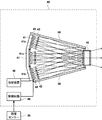
図2は、光源ユニットの一例を示す図である。光源ユニット40は、ベース基板41、半導体発光素子42、拡大レンズ43、フライアイレンズ45、制御回路46、冷却部材47、冷却装置48、及びミラー50を含んで構成されている。ベース基板41には、複数の半導体発光素子42が搭載されている。ベース基板41は、制御回路46の制御により、各半導体発光素子42を駆動する。各半導体発光素子42は、発光ダイオードやレーザーダイオード等から成り、露光光を形成する光を発生する。制御回路46は、照度センサー35の測定結果に基づき、各半導体発光素子42の駆動を制御する。
FIG. 2 is a diagram illustrating an example of a light source unit. The
なお、図2では、9個の半導体発光素子42が示されているが、実際の光源ユニットには、数百〜数千個程度の半導体発光素子が使用されている。
In FIG. 2, nine semiconductor
各半導体発光素子42に対応して、拡大レンズ43が設けられており、各拡大レンズ43は、各半導体発光素子42から発生した光を拡大して、フライアイレンズ45へ照射する。図3は、図2に示した光源ユニットの半導体発光素子及び拡大レンズの光軸の方向を示す図である。図3(a)の矢印は、ベース基板41を横から見たときの半導体発光素子42及び拡大レンズ43の光軸の方向を示している。また、図3(b)の矢印は、ベース基板41を正面から見たときの半導体発光素子42及び拡大レンズ43の光軸の方向を示している。
A magnifying
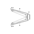
図3(b)に示す様に、ベース基板41は、複数の基板41a,41b,41cを組み合わせて構成されている。本例では、中央部の基板41aの上下及び左右に配置された基板41bが、図3(a)に示す様に、円筒の側面の一部を切り取った形状をしている。そして、中央部の基板41aの表面が、上下の基板41bの表面と左右の基板41bの表面とを組み合わせた形状をしている。基板41cは、平らであり、複数の半導体発光素子42が熱伝導部材47aを介して斜めに搭載されている。基板41a,41bに搭載された半導体発光素子42及びそれらに対応する拡大レンズ43の光軸は、図3(a),(b)に示す様に、フライアイレンズ45の中央へ向けて配置されている。基板41cに搭載された半導体発光素子42及びそれらに対応する拡大レンズ43の光軸は、図3(a),(b)に示す様に、フライアイレンズ45へ向けて互いに平行に配置されている。
As shown in FIG. 3B, the
図4は、光源ユニットの他の例を示す図である。また、図5は、図4に示した光源ユニットの半導体発光素子及び拡大レンズの光軸の方向を示す図である。図5(a)の矢印は、図5(b)に示したベース基板41のA−A部断面を見たときの半導体発光素子42及び拡大レンズ43の光軸の方向を示している。また、図5(b)の矢印は、ベース基板41を正面から見たときの半導体発光素子42及び拡大レンズ43の光軸の方向を示している。
FIG. 4 is a diagram illustrating another example of the light source unit. FIG. 5 is a diagram showing the directions of the optical axes of the semiconductor light emitting element and the magnifying lens of the light source unit shown in FIG. The arrows in FIG. 5A indicate the directions of the optical axes of the semiconductor
本例では、ベース基板41が、複数の平らな基板41a,41b,41cを組み合わせて構成されている。ベース基板41の外周部に位置する基板41b,41cは、フライアイレンズ45へ向けて傾斜して設置されている。拡大レンズ43は、基板41a,41b,41c毎にアレイ状に構成されている。各基板41a,41b,41cに搭載された半導体発光素子42及びそれらに対応する拡大レンズ43の光軸は、図5(a),(b)に示す様に、フライアイレンズ45へ向けて互いに平行に配置されている。複数の平らな基板41a,41b,41cを組み合わせてベース基板41を構成し、複数の拡大レンズ43を基板41a,41b,41c毎にアレイ状に構成するので、半導体発光素子42のベース基板41への実装が容易になり、かつ拡大レンズ43の光軸の調整が容易になる。
In this example, the
図2及び図4において、複数の拡大レンズ43からフライアイレンズ45までの光路を囲んで、ミラー50が設けられている。図2及び図4に示した例では、ベース基板41及びフライアイレンズ45が四角形であり、ベース基板41がフライアイレンズ45より大きいので、ミラー50は、四角錐の上部を切り取った形状をしている。ミラー50は、ベース基板41の外周部の基板41b、41cに搭載された半導体発光素子42から発生して対応する拡大レンズ43により拡大された光の一部を反射して、フライアイレンズ45へ照射する。
2 and 4, a
フライアイレンズ45は、複数の拡大レンズ43により拡大された光を重ね合わせて、照度分布が均一な露光光を形成する。このとき、フライアイレンズ45は、拡大レンズ43から直接入射した光と、ミラー50により反射されて入射した光とを合わせて、露光光を形成する。拡大レンズ43又はミラー50からフライアイレンズ45へ所定の角度αより大きな入射角度で入射した光は、フライアイレンズ45の照射面から外れ、露光光の形成に利用されない。
The fly-
ベース基板41の裏面には、冷却部材47が取り付けられている。冷却部材47は、内部に冷却水が流れる冷却水通路を有し、冷却装置48から冷却水通路へ供給される冷却水により、各半導体発光素子42を冷却する。なお、冷却部材47及び冷却装置48はこれに限らず、放熱板及び冷却ファンを含む空冷式としてもよい。
A cooling
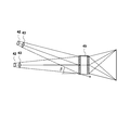
以下、本発明の一実施の形態によるプロキシミティ露光装置の露光光形成方法について説明する。図6は、本発明の一実施の形態によるプロキシミティ露光装置の露光光形成方法を説明する図である。本発明では、図6に示す様に、ベース基板41の外周部に搭載した半導体発光素子42及びそれらに対応する拡大レンズ43を、当該半導体発光素子42から発生して対応する拡大レンズ43により拡大された光の一方の端が、フライアイレンズ45の照射面から外れない所定の角度α以内でフライアイレンズ45へ入射する様に配置する。そして、ミラー50を、ベース基板41の外周部に搭載した半導体発光素子42から発生して対応する拡大レンズ43により拡大された光の他方の端が、当該ミラー50により反射されて、フライアイレンズ45の照射面から外れない所定の角度α以内でフライアイレンズ45へ入射する様に配置する。
Hereinafter, an exposure light forming method of a proximity exposure apparatus according to an embodiment of the present invention will be described. FIG. 6 is a view for explaining an exposure light forming method of the proximity exposure apparatus according to the embodiment of the present invention. In the present invention, as shown in FIG. 6, the semiconductor
ベース基板41の外周部に搭載した半導体発光素子42から発生して対応する拡大レンズ43により拡大された光の内、フライアイレンズ45の外周から当該光の一方の端までの間のフライアイレンズ45へ直接照射される光は、フライアイレンズ45の照射面から外れない所定の角度α以内でフライアイレンズ45へ入射して、露光光の形成に利用される。また、当該半導体発光素子42から発生して対応する拡大レンズ43により拡大された光の内、フライアイレンズ45の外周から当該光の他方の端までの間のフライアイレンズ45へ直接照射されない光は、ミラー50により反射されて、フライアイレンズ45の照射面から外れない所定の角度α以内でフライアイレンズ45へ入射して、露光光の形成に利用される。従って、複数の半導体発光素子42から発生して拡大レンズ43により拡大された光をフライアイレンズ45で重ね合わせる際、各半導体発光素子42の光が効率良く利用されて、照度の高い露光光が形成される。
Of the light generated from the semiconductor
さらに、本実施の形態では、図6に示す様に、ベース基板41の最外周に搭載した半導体発光素子42及びそれらに対応する拡大レンズ43の光軸を、フライアイレンズ45の外周へ向けて配置し、ミラー50を、当該光軸とほぼ平行に配置する。
Furthermore, in the present embodiment, as shown in FIG. 6, the optical axis of the semiconductor
図7は、ベース基板の最外周に搭載した半導体発光素子及びそれらに対応する拡大レンズの光軸を、フライアイレンズの外周よりも内側へ向けて配置した例を示す図である。ベース基板41の最外周に搭載した半導体発光素子42及びそれらに対応する拡大レンズ43の光軸を、フライアイレンズ45の外周よりも内側へ向けて配置した場合、当該半導体発光素子42から発生して対応する拡大レンズ43により拡大された光の一方の端を、所定の角度α以内でフライアイレンズ45へ入射させるためには、フライアイレンズ45から当該半導体発光素子42までの距離を長くする必要がある。
FIG. 7 is a diagram showing an example in which the optical axes of the semiconductor light emitting elements mounted on the outermost periphery of the base substrate and the magnifying lenses corresponding thereto are arranged inward from the outer periphery of the fly-eye lens. When the optical axis of the semiconductor
図6に示した実施の形態では、ベース基板41の最外周に搭載した半導体発光素子42及びそれらに対応する拡大レンズ43の光軸を、フライアイレンズ45の外周へ向けて配置するので、図7に示した例に比べ、当該半導体発光素子42から発生して対応する拡大レンズ43により拡大された光の一方の端を、所定の角度α以内でフライアイレンズ45へ入射させるために必要な、フライアイレンズ45から当該半導体発光素子42までの距離を小さくすることができる。
In the embodiment shown in FIG. 6, the optical axis of the semiconductor
以上説明した実施の形態によれば、複数の拡大レンズ43からフライアイレンズ45までの光路を囲んでミラー50を設け、ベース基板41の外周部に搭載した半導体発光素子42及びそれらに対応する拡大レンズ43を、当該半導体発光素子42から発生して対応する拡大レンズ43により拡大された光の一方の端が、フライアイレンズ45の照射面から外れない所定の角度α以内でフライアイレンズ45へ入射する様に配置し、ミラー50を、ベース基板41の外周部に搭載した半導体発光素子42から発生して対応する拡大レンズ43により拡大された光の他方の端が、当該ミラー50により反射されて、フライアイレンズ45の照射面から外れない所定の角度α以内でフライアイレンズ45へ入射する様に配置することにより、複数の半導体発光素子42から発生して拡大レンズ43により拡大された光をフライアイレンズ45で重ね合わせる際、各半導体発光素子42の光を効率良く利用して、照度の高い露光光を形成することができる。
According to the embodiment described above, the
さらに、ベース基板41の最外周に搭載した半導体発光素子42及びそれらに対応する拡大レンズ43の光軸を、フライアイレンズ45の外周へ向けて配置し、ミラー50を、当該光軸とほぼ平行に配置することにより、当該半導体発光素子42から発生して対応する拡大レンズ43により拡大された光の一方の端を、所定の角度α以内でフライアイレンズ45へ入射させるために必要な、フライアイレンズ45から当該半導体発光素子42までの距離を小さくすることができる。
Further, the optical axes of the semiconductor
さらに、図4に示した例によれば、複数の平らな基板41a,41b,41cを組み合わせてベース基板41を構成し、複数の拡大レンズを当該基板41a,41b,41c毎にアレイ状に構成することにより、半導体発光素子42をベース基板41に容易に実装することができ、かつ拡大レンズ43の光軸を容易に調整することができる。
Further, according to the example shown in FIG. 4, a plurality of
本発明のプロキシミティ露光装置を用いて露光を行い、あるいは、本発明のプロキシミティ露光装置の露光光形成方法を用いて形成した露光光をマスクを介して基板へ照射し、基板の露光を行うことにより、露光光の照度が増加して露光時間が短縮され、また露光光の光源の寿命が長くなるので、表示用パネル基板の生産性を向上させることができる。 The exposure is performed using the proximity exposure apparatus of the present invention, or the substrate is exposed by irradiating the substrate with exposure light formed using the exposure light forming method of the proximity exposure apparatus of the present invention through a mask. As a result, the illuminance of the exposure light is increased, the exposure time is shortened, and the life of the light source of the exposure light is increased, so that the productivity of the display panel substrate can be improved.
例えば、図8は、液晶ディスプレイ装置のTFT基板の製造工程の一例を示すフローチャートである。薄膜形成工程(ステップ101)では、スパッタ法やプラズマ化学気相成長(CVD)法等により、基板上に液晶駆動用の透明電極となる導電体膜や絶縁体膜等の薄膜を形成する。レジスト塗布工程(ステップ102)では、ロール塗布法等により感光樹脂材料(フォトレジスト)を塗布して、薄膜形成工程(ステップ101)で形成した薄膜上にフォトレジスト膜を形成する。露光工程(ステップ103)では、プロキシミティ露光装置や投影露光装置等を用いて、マスクのパターンをフォトレジスト膜に転写する。現像工程(ステップ104)では、シャワー現像法等により現像液をフォトレジスト膜上に供給して、フォトレジスト膜の不要部分を除去する。エッチング工程(ステップ105)では、ウエットエッチングにより、薄膜形成工程(ステップ101)で形成した薄膜の内、フォトレジスト膜でマスクされていない部分を除去する。剥離工程(ステップ106)では、エッチング工程(ステップ105)でのマスクの役目を終えたフォトレジスト膜を、剥離液によって剥離する。これらの各工程の前又は後には、必要に応じて、基板の洗浄/乾燥工程が実施される。これらの工程を数回繰り返して、基板上にTFTアレイが形成される。 For example, FIG. 8 is a flowchart showing an example of the manufacturing process of the TFT substrate of the liquid crystal display device. In the thin film formation step (step 101), a thin film such as a conductor film or an insulator film, which becomes a transparent electrode for driving liquid crystal, is formed on the substrate by sputtering, plasma chemical vapor deposition (CVD), or the like. In the resist coating process (step 102), a photosensitive resin material (photoresist) is applied by a roll coating method or the like to form a photoresist film on the thin film formed in the thin film forming process (step 101). In the exposure step (step 103), the mask pattern is transferred to the photoresist film using a proximity exposure apparatus, a projection exposure apparatus, or the like. In the development step (step 104), a developer is supplied onto the photoresist film by a shower development method or the like to remove unnecessary portions of the photoresist film. In the etching process (step 105), a portion of the thin film formed in the thin film formation process (step 101) that is not masked by the photoresist film is removed by wet etching. In the peeling step (step 106), the photoresist film that has finished the role of the mask in the etching step (step 105) is peeled off with a peeling solution. Before or after each of these steps, a substrate cleaning / drying step is performed as necessary. These steps are repeated several times to form a TFT array on the substrate.
また、図9は、液晶ディスプレイ装置のカラーフィルタ基板の製造工程の一例を示すフローチャートである。ブラックマトリクス形成工程(ステップ201)では、レジスト塗布、露光、現像、エッチング、剥離等の処理により、基板上にブラックマトリクスを形成する。着色パターン形成工程(ステップ202)では、染色法、顔料分散法、印刷法、電着法等により、基板上に着色パターンを形成する。この工程を、R、G、Bの着色パターンについて繰り返す。保護膜形成工程(ステップ203)では、着色パターンの上に保護膜を形成し、透明電極膜形成工程(ステップ204)では、保護膜の上に透明電極膜を形成する。これらの各工程の前、途中又は後には、必要に応じて、基板の洗浄/乾燥工程が実施される。 FIG. 9 is a flowchart showing an example of the manufacturing process of the color filter substrate of the liquid crystal display device. In the black matrix forming step (step 201), a black matrix is formed on the substrate by processing such as resist coating, exposure, development, etching, and peeling. In the colored pattern forming step (step 202), a colored pattern is formed on the substrate by a dyeing method, a pigment dispersion method, a printing method, an electrodeposition method, or the like. This process is repeated for the R, G, and B coloring patterns. In the protective film forming step (step 203), a protective film is formed on the colored pattern, and in the transparent electrode film forming step (step 204), a transparent electrode film is formed on the protective film. Before, during or after each of these steps, a substrate cleaning / drying step is performed as necessary.
図8に示したTFT基板の製造工程では、露光工程(ステップ103)において、図9に示したカラーフィルタ基板の製造工程では、ブラックマトリクス形成工程(ステップ201)及び着色パターン形成工程(ステップ202)の露光処理において、本発明のプロキシミティ露光装置又はプロキシミティ露光装置の露光光形成方法を適用することができる。 In the TFT substrate manufacturing process shown in FIG. 8, in the exposure process (step 103), in the color filter substrate manufacturing process shown in FIG. 9, in the black matrix forming process (step 201) and the colored pattern forming process (step 202). In this exposure process, the proximity exposure apparatus or the exposure light forming method of the proximity exposure apparatus of the present invention can be applied.
1 基板
2 マスク
3 ベース
4 Xガイド
5 Xステージ
6 Yガイド
7 Yステージ
8 θステージ
9 チャック支持台
10 チャック
20 マスクホルダ
30 露光光照射装置
32 コリメーションレンズ群
33 平面鏡
35 照度センサー
40 光源ユニット
41 ベース基板
41a,41b,41c 基板
42 半導体発光素子
43 拡大レンズ
45 フライアイレンズ
46 制御回路
47 冷却部材
47a 熱伝導部材
48 冷却装置
50 ミラー
DESCRIPTION OF SYMBOLS 1 Substrate 2 Mask 3 Base 4 X guide 5 X stage 6 Y guide 7
Claims (6)
前記複数の半導体発光素子を搭載するベース基板と、
各半導体発光素子に対応して設けられ、各半導体発光素子から発生した光を拡大する複数の拡大レンズと、
前記複数の拡大レンズにより拡大された光が照射されるフライアイレンズとを備え、
前記複数の拡大レンズにより拡大された光を前記フライアイレンズで重ね合わせて露光光を形成するプロキシミティ露光装置であって、
前記複数の拡大レンズから前記フライアイレンズまでの光路を囲んで設けられた反射部材を備え、
前記ベース基板の外周部に搭載された半導体発光素子及びそれらに対応する拡大レンズは、当該半導体発光素子から発生して対応する拡大レンズにより拡大された光の一方の端が、前記フライアイレンズの照射面から外れない所定の角度以内で前記フライアイレンズへ入射する様に配置され、
前記反射部材は、前記ベース基板の外周部に搭載された半導体発光素子から発生して対応する拡大レンズにより拡大された光の他方の端が、当該反射部材により反射されて、前記フライアイレンズの照射面から外れない所定の角度以内で前記フライアイレンズへ入射する様に配置され、かつ、
前記ベース基板の最外周に搭載された半導体発光素子及びそれらに対応する拡大レンズは、光軸が前記フライアイレンズの外周へ向けて配置され、
前記反射部材は、当該光軸とほぼ平行に配置されたことを特徴とするプロキシミティ露光装置。 A plurality of semiconductor light emitting elements that generate light that forms exposure light; and
A base substrate on which the plurality of semiconductor light emitting elements are mounted;
A plurality of magnifying lenses that are provided corresponding to each semiconductor light emitting element and that magnify light generated from each semiconductor light emitting element,
A fly-eye lens irradiated with light enlarged by the plurality of magnifying lenses,
A proximity exposure apparatus that forms exposure light by superimposing light expanded by the plurality of magnifying lenses on the fly-eye lens,
A reflective member provided around an optical path from the plurality of magnifying lenses to the fly-eye lens;
The semiconductor light emitting elements mounted on the outer periphery of the base substrate and the magnifying lenses corresponding thereto have one end of light generated from the semiconductor light emitting elements and enlarged by the corresponding magnifying lens, of the fly eye lens. Arranged to enter the fly-eye lens within a predetermined angle that does not deviate from the irradiation surface,
The reflection member is configured such that the other end of the light generated from the semiconductor light emitting element mounted on the outer peripheral portion of the base substrate and magnified by the corresponding magnification lens is reflected by the reflection member, and the fly-eye lens Arranged to enter the fly-eye lens within a predetermined angle that does not deviate from the irradiation surface , and
The semiconductor light emitting elements mounted on the outermost periphery of the base substrate and the magnifying lenses corresponding to them are arranged with the optical axis facing the outer periphery of the fly-eye lens,
The proximity exposure apparatus , wherein the reflecting member is disposed substantially parallel to the optical axis .
各半導体発光素子に対応して複数の拡大レンズを設け、各半導体発光素子から発生した光を対応する拡大レンズにより拡大して、フライアイレンズへ照射し、
複数の拡大レンズにより拡大した光をフライアイレンズで重ね合わせて露光光を形成するプロキシミティ露光装置の露光光形成方法であって、
複数の拡大レンズからフライアイレンズまでの光路を囲んで反射部材を設け、
ベース基板の外周部に搭載した半導体発光素子及びそれらに対応する拡大レンズを、当該半導体発光素子から発生して対応する拡大レンズにより拡大された光の一方の端が、フライアイレンズの照射面から外れない所定の角度以内でフライアイレンズへ入射する様に配置し、
反射部材を、ベース基板の外周部に搭載した半導体発光素子から発生して対応する拡大レンズにより拡大された光の他方の端が、当該反射部材により反射されて、フライアイレンズの照射面から外れない所定の角度以内でフライアイレンズへ入射する様に配置し、かつ、
ベース基板の最外周に搭載した半導体発光素子及びそれらに対応する拡大レンズの光軸を、フライアイレンズの外周へ向けて配置し、
反射部材を、当該光軸とほぼ平行に配置することを特徴とするプロキシミティ露光装置の露光光形成方法。 A plurality of semiconductor light emitting elements are mounted on a base substrate, and light forming exposure light is generated from each semiconductor light emitting element,
A plurality of magnifying lenses are provided corresponding to each semiconductor light emitting element, the light generated from each semiconductor light emitting element is magnified by the corresponding magnifying lens, and irradiated to the fly-eye lens,
An exposure light forming method of a proximity exposure apparatus that forms exposure light by overlapping light expanded by a plurality of magnifying lenses with a fly-eye lens,
A reflecting member is provided around the optical path from the plurality of magnifying lenses to the fly-eye lens,
One end of light generated from the semiconductor light emitting element and magnified by the corresponding magnifying lens from the semiconductor light emitting element mounted on the outer periphery of the base substrate and the corresponding magnifying lens from the irradiation surface of the fly-eye lens Place it so that it enters the fly-eye lens within a predetermined angle that does not come off,
The other end of the light generated from the semiconductor light emitting element mounted on the outer peripheral portion of the base substrate and enlarged by the corresponding magnifying lens is reflected by the reflecting member and deviates from the irradiation surface of the fly-eye lens. Arranged to enter the fly-eye lens within a predetermined angle , and
The optical axis of the semiconductor light emitting element mounted on the outermost periphery of the base substrate and the magnifying lens corresponding to them is arranged toward the outer periphery of the fly-eye lens,
An exposure light forming method for a proximity exposure apparatus , wherein a reflecting member is disposed substantially parallel to the optical axis .
Priority Applications (4)
| Application Number | Priority Date | Filing Date | Title |
|---|---|---|---|
| JP2009160727A JP5355261B2 (en) | 2009-07-07 | 2009-07-07 | Proximity exposure apparatus, exposure light forming method for proximity exposure apparatus, and display panel substrate manufacturing method |
| KR1020100058848A KR101133371B1 (en) | 2009-07-07 | 2010-06-22 | Proximity exposure apparatus, method of forming exposure light in the proximity exposure apparatus and method of manufacturing a display panel substrate |
| CN2010102153535A CN101943867B (en) | 2009-07-07 | 2010-06-25 | Adjacent exposure device, forming method of exposure beam and manufacturing method of panel substrate |
| TW099121055A TWI414903B (en) | 2009-07-07 | 2010-06-28 | Proximity exposure device, its exposure beam forming method and manufacturing method of a display panel substrate |
Applications Claiming Priority (1)
| Application Number | Priority Date | Filing Date | Title |
|---|---|---|---|
| JP2009160727A JP5355261B2 (en) | 2009-07-07 | 2009-07-07 | Proximity exposure apparatus, exposure light forming method for proximity exposure apparatus, and display panel substrate manufacturing method |
Publications (2)
| Publication Number | Publication Date |
|---|---|
| JP2011017770A JP2011017770A (en) | 2011-01-27 |
| JP5355261B2 true JP5355261B2 (en) | 2013-11-27 |
Family
ID=43435914
Family Applications (1)
| Application Number | Title | Priority Date | Filing Date |
|---|---|---|---|
| JP2009160727A Expired - Fee Related JP5355261B2 (en) | 2009-07-07 | 2009-07-07 | Proximity exposure apparatus, exposure light forming method for proximity exposure apparatus, and display panel substrate manufacturing method |
Country Status (4)
| Country | Link |
|---|---|
| JP (1) | JP5355261B2 (en) |
| KR (1) | KR101133371B1 (en) |
| CN (1) | CN101943867B (en) |
| TW (1) | TWI414903B (en) |
Families Citing this family (4)
| Publication number | Priority date | Publication date | Assignee | Title |
|---|---|---|---|---|
| JP2013171088A (en) * | 2012-02-17 | 2013-09-02 | Hitachi High-Technologies Corp | Proximity exposure apparatus, method for forming exposure light of proximity exposure apparatus, and method for manufacturing display panel substrate |
| KR101649129B1 (en) * | 2015-08-21 | 2016-08-18 | (주)블루코어 | UV LED light source module unit for exposure photolithography process and exposure photolithography apparatus used the same |
| DE102017217345B4 (en) | 2017-09-28 | 2019-12-24 | Fraunhofer-Gesellschaft zur Förderung der angewandten Forschung e.V. | Optical beam former |
| CN110196517B (en) * | 2019-05-16 | 2021-09-03 | Tcl华星光电技术有限公司 | Ultraviolet irradiation machine |
Family Cites Families (18)
| Publication number | Priority date | Publication date | Assignee | Title |
|---|---|---|---|---|
| JPH07301800A (en) * | 1994-05-10 | 1995-11-14 | Fujitsu General Ltd | Light source device for liquid crystal projector |
| JPH10261577A (en) * | 1997-03-21 | 1998-09-29 | Nikon Corp | Method for controlling amount of exposure and scanning-type aligner using it |
| KR20010043176A (en) * | 1999-03-02 | 2001-05-25 | 모리시타 요이찌 | Illuminating device and display device provided with the device |
| TW418343B (en) * | 1999-11-16 | 2001-01-11 | Nippon Kogaku Kk | The method of projection exposure and device thereof and projection optics system |
| JP2001343706A (en) * | 2000-05-31 | 2001-12-14 | Sony Corp | Video display device |
| JP2005533365A (en) * | 2001-11-07 | 2005-11-04 | アプライド マテリアルズ インコーポレイテッド | Maskless photon-electron spot grating array printing device |
| JP2003330109A (en) * | 2002-05-09 | 2003-11-19 | Seiko Epson Corp | Illuminator and projection type display device |
| TWI242690B (en) * | 2002-08-15 | 2005-11-01 | Asml Netherlands Bv | Reflector assembly, lithographic projection apparatus, radiation system with the reflector assembly, and method of manufacturing an integrated structure by a lithographic process |
| JP2004133127A (en) * | 2002-10-09 | 2004-04-30 | Sharp Corp | Exposure device |
| JP2009009144A (en) * | 2003-04-11 | 2009-01-15 | Ricoh Co Ltd | Document reading device and image forming apparatus |
| JP4328320B2 (en) * | 2004-09-03 | 2009-09-09 | サンエー技研株式会社 | Light source for exposure |
| JP2007072371A (en) * | 2005-09-09 | 2007-03-22 | V Technology Co Ltd | Exposure apparatus |
| JP2008070769A (en) * | 2006-09-15 | 2008-03-27 | Ricoh Co Ltd | Light source unit, illumination device and projector device |
| JP4749299B2 (en) * | 2006-09-28 | 2011-08-17 | 株式会社日立ハイテクノロジーズ | Exposure apparatus, exposure method, and manufacturing method of display panel substrate |
| JP5282368B2 (en) * | 2007-01-31 | 2013-09-04 | 株式会社リコー | Image reading apparatus and image forming apparatus |
| KR20090115712A (en) * | 2007-02-20 | 2009-11-05 | 칼 짜이스 에스엠테 아게 | Optical element with multiple primary light sources |
| JP4937808B2 (en) * | 2007-03-26 | 2012-05-23 | フェニックス電機株式会社 | Light source device and exposure apparatus using the same |
| JP5345443B2 (en) * | 2009-04-21 | 2013-11-20 | 株式会社日立ハイテクノロジーズ | Exposure apparatus, exposure light irradiation method, and display panel substrate manufacturing method |
-
2009
- 2009-07-07 JP JP2009160727A patent/JP5355261B2/en not_active Expired - Fee Related
-
2010
- 2010-06-22 KR KR1020100058848A patent/KR101133371B1/en not_active IP Right Cessation
- 2010-06-25 CN CN2010102153535A patent/CN101943867B/en not_active Expired - Fee Related
- 2010-06-28 TW TW099121055A patent/TWI414903B/en not_active IP Right Cessation
Also Published As
| Publication number | Publication date |
|---|---|
| TWI414903B (en) | 2013-11-11 |
| TW201102767A (en) | 2011-01-16 |
| JP2011017770A (en) | 2011-01-27 |
| CN101943867A (en) | 2011-01-12 |
| CN101943867B (en) | 2012-11-07 |
| KR20110004276A (en) | 2011-01-13 |
| KR101133371B1 (en) | 2012-04-06 |
Similar Documents
| Publication | Publication Date | Title |
|---|---|---|
| JP5345443B2 (en) | Exposure apparatus, exposure light irradiation method, and display panel substrate manufacturing method | |
| US8797510B2 (en) | Gradient refractive index lens array projection exposure | |
| JP4863948B2 (en) | Exposure apparatus, exposure method, and manufacturing method of display panel substrate | |
| JP4749299B2 (en) | Exposure apparatus, exposure method, and manufacturing method of display panel substrate | |
| TWI608309B (en) | Uv led light source module unit for exposure photolithography process and exposure photolithography apparatus used the same | |
| JP2007033882A (en) | Exposure device and exposure method, and manufacturing method for wiring board | |
| JP2006351586A (en) | Lighting device, projection aligner, and method of manufacturing microdevice | |
| TW200937141A (en) | Exposure apparatus, exposure method and device manufacturing method | |
| JP5355261B2 (en) | Proximity exposure apparatus, exposure light forming method for proximity exposure apparatus, and display panel substrate manufacturing method | |
| JP2013171088A (en) | Proximity exposure apparatus, method for forming exposure light of proximity exposure apparatus, and method for manufacturing display panel substrate | |
| JP2011134932A (en) | Light source unit, exposure light irradiating device, exposure device, method of manufacturing display panel substrate, device and method of inspecting semiconductor light emitting element section | |
| JP5394320B2 (en) | Light source unit, optical axis adjustment method of light source unit, proximity exposure apparatus, exposure light irradiation method of proximity exposure apparatus, and manufacturing method of display panel substrate | |
| JP2011242563A (en) | Exposure apparatus, method for positioning lamp of exposure apparatus, and method of manufacturing display panel substrate | |
| JP5456620B2 (en) | Proximity exposure apparatus, exposure light irradiation method for proximity exposure apparatus, and method for manufacturing display panel substrate | |
| JP2012220619A (en) | Exposure apparatus, exposure method, and method for manufacturing display panel substrate | |
| JPWO2009150913A1 (en) | Illumination apparatus, exposure apparatus, and device manufacturing method | |
| JP5306020B2 (en) | Proximity exposure apparatus, substrate moving method of proximity exposure apparatus, and display panel substrate manufacturing method | |
| JP2011237596A (en) | Exposure apparatus, exposure method, and manufacturing method of display panel substrate | |
| JP2012252296A (en) | Proximity exposure apparatus, method for applying exposure light of proximity exposure apparatus, and method for manufacturing display panel substrate | |
| JP2013200529A (en) | Proximity exposure device, exposure light irradiation method of the same, and manufacturing method of display panel substrate | |
| JP2003076030A (en) | Light irradiation device for exposure device | |
| JP2014149391A (en) | Pattern forming apparatus and pattern forming method |
Legal Events
| Date | Code | Title | Description |
|---|---|---|---|
| A621 | Written request for application examination |
Free format text: JAPANESE INTERMEDIATE CODE: A621 Effective date: 20111005 |
|
| A977 | Report on retrieval |
Free format text: JAPANESE INTERMEDIATE CODE: A971007 Effective date: 20130628 |
|
| A131 | Notification of reasons for refusal |
Free format text: JAPANESE INTERMEDIATE CODE: A131 Effective date: 20130702 |
|
| A521 | Written amendment |
Free format text: JAPANESE INTERMEDIATE CODE: A523 Effective date: 20130812 |
|
| TRDD | Decision of grant or rejection written | ||
| A01 | Written decision to grant a patent or to grant a registration (utility model) |
Free format text: JAPANESE INTERMEDIATE CODE: A01 Effective date: 20130827 |
|
| A61 | First payment of annual fees (during grant procedure) |
Free format text: JAPANESE INTERMEDIATE CODE: A61 Effective date: 20130827 |
|
| R150 | Certificate of patent or registration of utility model |
Free format text: JAPANESE INTERMEDIATE CODE: R150 |
|
| LAPS | Cancellation because of no payment of annual fees |