JP5342111B2 - 有機el表示装置 - Google Patents
有機el表示装置 Download PDFInfo
- Publication number
- JP5342111B2 JP5342111B2 JP2007060395A JP2007060395A JP5342111B2 JP 5342111 B2 JP5342111 B2 JP 5342111B2 JP 2007060395 A JP2007060395 A JP 2007060395A JP 2007060395 A JP2007060395 A JP 2007060395A JP 5342111 B2 JP5342111 B2 JP 5342111B2
- Authority
- JP
- Japan
- Prior art keywords
- tft
- organic
- switch
- precharge
- voltage
- Prior art date
- Legal status (The legal status is an assumption and is not a legal conclusion. Google has not performed a legal analysis and makes no representation as to the accuracy of the status listed.)
- Active
Links
- 239000003990 capacitor Substances 0.000 claims description 19
- 238000001514 detection method Methods 0.000 claims description 16
- 239000000758 substrate Substances 0.000 claims description 6
- 239000011159 matrix material Substances 0.000 claims description 4
- 235000019557 luminance Nutrition 0.000 description 51
- 230000005669 field effect Effects 0.000 description 14
- 238000010586 diagram Methods 0.000 description 8
- 238000005259 measurement Methods 0.000 description 7
- 230000006866 deterioration Effects 0.000 description 6
- 238000000034 method Methods 0.000 description 4
- 238000007796 conventional method Methods 0.000 description 2
- 238000007689 inspection Methods 0.000 description 2
- 239000004973 liquid crystal related substance Substances 0.000 description 2
- 238000005401 electroluminescence Methods 0.000 description 1
- 230000006870 function Effects 0.000 description 1
- 230000002250 progressing effect Effects 0.000 description 1
- 238000005215 recombination Methods 0.000 description 1
- 230000006798 recombination Effects 0.000 description 1
- 230000004044 response Effects 0.000 description 1
- 238000004904 shortening Methods 0.000 description 1
- 239000010409 thin film Substances 0.000 description 1
- 239000013585 weight reducing agent Substances 0.000 description 1
Images


Classifications
-
- G—PHYSICS
- G09—EDUCATION; CRYPTOGRAPHY; DISPLAY; ADVERTISING; SEALS
- G09G—ARRANGEMENTS OR CIRCUITS FOR CONTROL OF INDICATING DEVICES USING STATIC MEANS TO PRESENT VARIABLE INFORMATION
- G09G3/00—Control arrangements or circuits, of interest only in connection with visual indicators other than cathode-ray tubes
- G09G3/20—Control arrangements or circuits, of interest only in connection with visual indicators other than cathode-ray tubes for presentation of an assembly of a number of characters, e.g. a page, by composing the assembly by combination of individual elements arranged in a matrix no fixed position being assigned to or needed to be assigned to the individual characters or partial characters
- G09G3/22—Control arrangements or circuits, of interest only in connection with visual indicators other than cathode-ray tubes for presentation of an assembly of a number of characters, e.g. a page, by composing the assembly by combination of individual elements arranged in a matrix no fixed position being assigned to or needed to be assigned to the individual characters or partial characters using controlled light sources
- G09G3/30—Control arrangements or circuits, of interest only in connection with visual indicators other than cathode-ray tubes for presentation of an assembly of a number of characters, e.g. a page, by composing the assembly by combination of individual elements arranged in a matrix no fixed position being assigned to or needed to be assigned to the individual characters or partial characters using controlled light sources using electroluminescent panels
- G09G3/32—Control arrangements or circuits, of interest only in connection with visual indicators other than cathode-ray tubes for presentation of an assembly of a number of characters, e.g. a page, by composing the assembly by combination of individual elements arranged in a matrix no fixed position being assigned to or needed to be assigned to the individual characters or partial characters using controlled light sources using electroluminescent panels semiconductive, e.g. using light-emitting diodes [LED]
- G09G3/3208—Control arrangements or circuits, of interest only in connection with visual indicators other than cathode-ray tubes for presentation of an assembly of a number of characters, e.g. a page, by composing the assembly by combination of individual elements arranged in a matrix no fixed position being assigned to or needed to be assigned to the individual characters or partial characters using controlled light sources using electroluminescent panels semiconductive, e.g. using light-emitting diodes [LED] organic, e.g. using organic light-emitting diodes [OLED]
- G09G3/3225—Control arrangements or circuits, of interest only in connection with visual indicators other than cathode-ray tubes for presentation of an assembly of a number of characters, e.g. a page, by composing the assembly by combination of individual elements arranged in a matrix no fixed position being assigned to or needed to be assigned to the individual characters or partial characters using controlled light sources using electroluminescent panels semiconductive, e.g. using light-emitting diodes [LED] organic, e.g. using organic light-emitting diodes [OLED] using an active matrix
- G09G3/3233—Control arrangements or circuits, of interest only in connection with visual indicators other than cathode-ray tubes for presentation of an assembly of a number of characters, e.g. a page, by composing the assembly by combination of individual elements arranged in a matrix no fixed position being assigned to or needed to be assigned to the individual characters or partial characters using controlled light sources using electroluminescent panels semiconductive, e.g. using light-emitting diodes [LED] organic, e.g. using organic light-emitting diodes [OLED] using an active matrix with pixel circuitry controlling the current through the light-emitting element
-
- G—PHYSICS
- G09—EDUCATION; CRYPTOGRAPHY; DISPLAY; ADVERTISING; SEALS
- G09G—ARRANGEMENTS OR CIRCUITS FOR CONTROL OF INDICATING DEVICES USING STATIC MEANS TO PRESENT VARIABLE INFORMATION
- G09G2300/00—Aspects of the constitution of display devices
- G09G2300/08—Active matrix structure, i.e. with use of active elements, inclusive of non-linear two terminal elements, in the pixels together with light emitting or modulating elements
- G09G2300/0809—Several active elements per pixel in active matrix panels
- G09G2300/0819—Several active elements per pixel in active matrix panels used for counteracting undesired variations, e.g. feedback or autozeroing
-
- G—PHYSICS
- G09—EDUCATION; CRYPTOGRAPHY; DISPLAY; ADVERTISING; SEALS
- G09G—ARRANGEMENTS OR CIRCUITS FOR CONTROL OF INDICATING DEVICES USING STATIC MEANS TO PRESENT VARIABLE INFORMATION
- G09G2300/00—Aspects of the constitution of display devices
- G09G2300/08—Active matrix structure, i.e. with use of active elements, inclusive of non-linear two terminal elements, in the pixels together with light emitting or modulating elements
- G09G2300/0809—Several active elements per pixel in active matrix panels
- G09G2300/0842—Several active elements per pixel in active matrix panels forming a memory circuit, e.g. a dynamic memory with one capacitor
- G09G2300/0852—Several active elements per pixel in active matrix panels forming a memory circuit, e.g. a dynamic memory with one capacitor being a dynamic memory with more than one capacitor
-
- G—PHYSICS
- G09—EDUCATION; CRYPTOGRAPHY; DISPLAY; ADVERTISING; SEALS
- G09G—ARRANGEMENTS OR CIRCUITS FOR CONTROL OF INDICATING DEVICES USING STATIC MEANS TO PRESENT VARIABLE INFORMATION
- G09G2310/00—Command of the display device
- G09G2310/02—Addressing, scanning or driving the display screen or processing steps related thereto
- G09G2310/0243—Details of the generation of driving signals
- G09G2310/0251—Precharge or discharge of pixel before applying new pixel voltage
-
- G—PHYSICS
- G09—EDUCATION; CRYPTOGRAPHY; DISPLAY; ADVERTISING; SEALS
- G09G—ARRANGEMENTS OR CIRCUITS FOR CONTROL OF INDICATING DEVICES USING STATIC MEANS TO PRESENT VARIABLE INFORMATION
- G09G2320/00—Control of display operating conditions
- G09G2320/02—Improving the quality of display appearance
- G09G2320/0223—Compensation for problems related to R-C delay and attenuation in electrodes of matrix panels, e.g. in gate electrodes or on-substrate video signal electrodes
-
- G—PHYSICS
- G09—EDUCATION; CRYPTOGRAPHY; DISPLAY; ADVERTISING; SEALS
- G09G—ARRANGEMENTS OR CIRCUITS FOR CONTROL OF INDICATING DEVICES USING STATIC MEANS TO PRESENT VARIABLE INFORMATION
- G09G2320/00—Control of display operating conditions
- G09G2320/06—Adjustment of display parameters
- G09G2320/0626—Adjustment of display parameters for control of overall brightness
-
- G—PHYSICS
- G09—EDUCATION; CRYPTOGRAPHY; DISPLAY; ADVERTISING; SEALS
- G09G—ARRANGEMENTS OR CIRCUITS FOR CONTROL OF INDICATING DEVICES USING STATIC MEANS TO PRESENT VARIABLE INFORMATION
- G09G3/00—Control arrangements or circuits, of interest only in connection with visual indicators other than cathode-ray tubes
- G09G3/20—Control arrangements or circuits, of interest only in connection with visual indicators other than cathode-ray tubes for presentation of an assembly of a number of characters, e.g. a page, by composing the assembly by combination of individual elements arranged in a matrix no fixed position being assigned to or needed to be assigned to the individual characters or partial characters
- G09G3/22—Control arrangements or circuits, of interest only in connection with visual indicators other than cathode-ray tubes for presentation of an assembly of a number of characters, e.g. a page, by composing the assembly by combination of individual elements arranged in a matrix no fixed position being assigned to or needed to be assigned to the individual characters or partial characters using controlled light sources
- G09G3/30—Control arrangements or circuits, of interest only in connection with visual indicators other than cathode-ray tubes for presentation of an assembly of a number of characters, e.g. a page, by composing the assembly by combination of individual elements arranged in a matrix no fixed position being assigned to or needed to be assigned to the individual characters or partial characters using controlled light sources using electroluminescent panels
- G09G3/32—Control arrangements or circuits, of interest only in connection with visual indicators other than cathode-ray tubes for presentation of an assembly of a number of characters, e.g. a page, by composing the assembly by combination of individual elements arranged in a matrix no fixed position being assigned to or needed to be assigned to the individual characters or partial characters using controlled light sources using electroluminescent panels semiconductive, e.g. using light-emitting diodes [LED]
- G09G3/3208—Control arrangements or circuits, of interest only in connection with visual indicators other than cathode-ray tubes for presentation of an assembly of a number of characters, e.g. a page, by composing the assembly by combination of individual elements arranged in a matrix no fixed position being assigned to or needed to be assigned to the individual characters or partial characters using controlled light sources using electroluminescent panels semiconductive, e.g. using light-emitting diodes [LED] organic, e.g. using organic light-emitting diodes [OLED]
- G09G3/3275—Details of drivers for data electrodes
- G09G3/3283—Details of drivers for data electrodes in which the data driver supplies a variable data current for setting the current through, or the voltage across, the light-emitting elements
Description
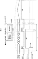
ことを特徴とする画像表示装置。
多結晶Si-TFT(Thin-Film-Transistor)を用いて透明基板上に設けられている
ことを特徴とする画像表示装置。
前記画素領域に表示信号を入力する信号線と、
表示信号電圧を駆動する表示信号駆動部と、
前記、画素領域に駆動制御信号を入力するため制御線と、
前記、駆動制御信号を駆動するための制御信号駆動部と
前記信号線を介して前記画素に入力された画像データ信号を基に、前期自発光素子を駆動するための電界効果トランジスタを有する画像表示装置であって、
前記電界効果トランジスタのソース電極には、基準電位が印加され、ゲート電極には、前記電界効果トランジスタのゲートとドレインを接続するための第1のスイッチ手段と、容量が接続され、ドレイン電極には、自発光素子への画像データ信号に基づく電流の供給を制御する第3のスイッチ手段が接続され、
前記自発光素子は陽極と陰極を有し、前記陽極には前記第3のスイッチ手段と、外部からの所定の電圧を印加するための第2のスイッチ手段が接続されている表示装置において、
前記、制御信号駆動部は、複数の発光輝度に関わる電圧や信号に応じて、駆動制御信号を可変する手段を有することを特徴とする画像表示装置。
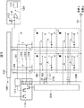
多結晶Si-TFT(Thin-Film-Transistor)を用いて透明基板上に設けられている
ことを特徴とする画像表示装置。
前記画素領域に表示信号を入力する信号線と、
表示信号電圧を駆動する表示信号駆動部と、
前記、画素領域に駆動制御信号を入力するため制御線と、
前記、駆動制御信号を駆動するための制御信号駆動部と
前記信号線を介して前記画素に入力された画像データ信号を基に、前期自発光素子を駆動するための電界効果トランジスタを有する画像表示装置であって、
前記電界効果トランジスタのソース電極には、基準電位が印加され、ゲート電極には、前記電界効果トランジスタのゲートとドレインを接続するためのリセットスイッチと、容量が接続され、ドレイン電極には、自発光素子への画像データ信号に基づく電流の供給を制御する第3のスイッチ手段が接続され、
前記自発光素子は陽極と陰極を有し、前記陰極には前記第3のスイッチ手段と、外部からの所定の電圧を印加するための第2のスイッチ手段が接続されている表示装置において、
前記、制御信号駆動部は、複数の発光輝度に関わる電圧や信号に応じて、駆動制御信号を可変する手段を有することを特徴とする画像表示装置。
多結晶Si-TFT(Thin-Film-Transistor)を用いて透明基板上に設けられている
ことを特徴とする画像表示装置。
Claims (6)
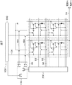
- 有機EL発光素子を有する複数の画素がマトリクス状に形成されている表示部と、
前記表示部に表示信号電圧を入力するための信号線と、
前記信号線に前記表示信号電圧を供給する表示信号駆動回路と、
前記有機EL発光素子に電源線を介して電流を供給する電源を有し、
前記電源の電圧を切り替えることによって、前記表示部を第1の最高輝度を有する標準モードと、前記第1の最高輝度よりも輝度の大きい第2の最高輝度を有する高輝度モードに切り替えることが出来る切り替え手段を有する有機EL表示装置であって、
前記画素は、前記有機EL発光素子と点灯TFTスイッチと前記有機EL発光素子を駆動する駆動TFTとが直列に接続され、前記点灯TFTスイッチは前記駆動TFTのドレイン電極と接続し、
前記電源の電圧は前記有機EL発光素子の陽極に接続し、前記駆動TFTのソース電極は基準電圧と接続し、
前記駆動TFTのドレイン電極とゲート電極の間にリセットTFTスイッチが接続され、前記有機EL発光素子と前記点灯TFTスイッチの接続部と、前記信号線の間にプリチャージTFTスイッチが接続され、
前記駆動TFTのゲートと前記リセットTFTスイッチの接続部と前記信号線との間に保持容量が接続され、
ゲート駆動回路からは前記リセットTFTスイッチのゲート電極と接続するリセット線と、前記プリチャージTFTスイッチのゲート電極と接続するプリチャージ接続線が延在し、
前記ゲート駆動回路は、前記切り替え手段からの信号を受けて、前記標準モードの場合は、前記リセットTFTスイッチをONすることにより、前記表示部の前記画素に前記表示信号電圧を入力する初期において、プリチャージ線を介して前記プリチャージTFTスイッチをONしてプリチャージを行って前記駆動TFTのゲート電極に前記基準電圧を印加し、
前記高輝度モードの場合は、前記プリチャージを行わない、手段を有することを特徴とする有機EL表示装置。 - 請求項1において、
前記駆動TFTは、多結晶Si-TFTを用いて透明基板上に設けられていることを特徴とする有機EL表示装置。 - 請求項1において、
前記プリチャージTFTスイッチを制御することによって、有機EL発光素子の電流電圧特性を測定することができる検出回路との接続をすることを特徴とする有機EL表示装置。 - 有機EL発光素子を有する複数の画素がマトリクス状に形成されている表示部と、
前記表示部に表示信号電圧を入力するための信号線と、
前記信号線に前記表示信号電圧を供給する表示信号駆動回路と、
前記画素に電源線を介して電流を供給する電源を有し、
前記電源の電圧を切り替えることによって、前記表示部を第1の最高輝度を有する標準モードと、前記第1の最高輝度よりも輝度の大きい第2の最高輝度を有する高輝度モードに切り替えることが出来る切り替え手段を有する有機EL表示装置であって、
前記画素は、前記電源線から順に、前記有機EL発光素子を駆動する駆動TFTと点灯TFTスイッチと前記有機EL発光素子とが直列に接続され、
前記駆動TFTのソース電極には電源電圧が印加され、前記駆動TFTのゲート電極と前記信号線との間には前記画素を選択するセレクトスイッチと容量が直列に接続し、
前記駆動TFTのゲート電極とドレイン電極の間にはリセットTFTスイッチが接続し、
前記駆動TFTのドレイン電極と前記有機EL発光素子の陽極の間には有機EL発光素子への電流の供給を制御する点灯TFTスイッチが接続し、
前記有機EL発光素子の前記陽極と前記信号線の間にはプリチャージTFTスイッチが接続され、
ゲート駆動回路からは前記リセットTFTスイッチのゲート電極と接続するリセット線と、前記プリチャージTFTスイッチのゲート電極と接続するプリチャージ接続線が延在し、
前記ゲート駆動回路は、前記切り替え手段からの信号を受けて、前記標準モードの場合は、前記リセットTFTスイッチをONすることにより、前記表示部の前記画素に前記表示信号電圧を入力する初期において、プリチャージ線を介して前記プリチャージTFTスイッチをONしてプリチャージを行って前記駆動TFTのゲート電極に基準電圧を印加し、
前記高輝度モードの場合は、前記プリチャージを行わない手段を有することを特徴とする有機EL表示装置。 - 請求項4において、
前記プリチャージTFTスイッチを制御することによって、有機EL発光素子の電流電圧特性を測定することができる検出回路との接続をすることを特徴とする有機EL表示装置。 - 請求項4において、
前記駆動TFTは、多結晶Si-TFTを用いて透明基板上に設けられていることを特徴とする有機EL表示装置。
Priority Applications (3)
| Application Number | Priority Date | Filing Date | Title |
|---|---|---|---|
| JP2007060395A JP5342111B2 (ja) | 2007-03-09 | 2007-03-09 | 有機el表示装置 |
| US12/003,373 US8063857B2 (en) | 2007-03-09 | 2007-12-21 | Image display apparatus |
| CN2008100020527A CN101261804B (zh) | 2007-03-09 | 2008-01-09 | 图像显示装置 |
Applications Claiming Priority (1)
| Application Number | Priority Date | Filing Date | Title |
|---|---|---|---|
| JP2007060395A JP5342111B2 (ja) | 2007-03-09 | 2007-03-09 | 有機el表示装置 |
Publications (2)
| Publication Number | Publication Date |
|---|---|
| JP2008224864A JP2008224864A (ja) | 2008-09-25 |
| JP5342111B2 true JP5342111B2 (ja) | 2013-11-13 |
Family
ID=39741133
Family Applications (1)
| Application Number | Title | Priority Date | Filing Date |
|---|---|---|---|
| JP2007060395A Active JP5342111B2 (ja) | 2007-03-09 | 2007-03-09 | 有機el表示装置 |
Country Status (3)
| Country | Link |
|---|---|
| US (1) | US8063857B2 (ja) |
| JP (1) | JP5342111B2 (ja) |
| CN (1) | CN101261804B (ja) |
Families Citing this family (21)
| Publication number | Priority date | Publication date | Assignee | Title |
|---|---|---|---|---|
| US8179343B2 (en) * | 2007-06-29 | 2012-05-15 | Canon Kabushiki Kaisha | Display apparatus and driving method of display apparatus |
| KR100894606B1 (ko) | 2007-10-29 | 2009-04-24 | 삼성모바일디스플레이주식회사 | 유기 전계 발광 표시 장치 및 그의 전원 공급 방법 |
| CN101903933B (zh) | 2008-01-07 | 2013-03-27 | 松下电器产业株式会社 | 显示装置、电子装置及驱动方法 |
| JP4816744B2 (ja) * | 2008-03-31 | 2011-11-16 | カシオ計算機株式会社 | 発光装置、表示装置、及び発光装置の駆動制御方法 |
| JP5260230B2 (ja) * | 2008-10-16 | 2013-08-14 | グローバル・オーエルイーディー・テクノロジー・リミテッド・ライアビリティ・カンパニー | 表示装置 |
| JP2010097059A (ja) * | 2008-10-17 | 2010-04-30 | Hitachi Displays Ltd | 表示装置 |
| JP2010145709A (ja) * | 2008-12-18 | 2010-07-01 | Hitachi Displays Ltd | 画像表示装置 |
| KR101732041B1 (ko) | 2010-11-19 | 2017-05-04 | 삼성디스플레이 주식회사 | 입체 영상 표시 장치 |
| CN103236237B (zh) * | 2013-04-26 | 2015-04-08 | 京东方科技集团股份有限公司 | 一种像素单元电路及其补偿方法、以及显示装置 |
| US9584046B2 (en) * | 2013-07-04 | 2017-02-28 | Nxp Usa, Inc. | Gate drive circuit and a method for controlling a power transistor |
| KR102170556B1 (ko) * | 2014-10-23 | 2020-10-28 | 엘지디스플레이 주식회사 | 표시장치 및 그 구동방법 |
| CN104464616B (zh) | 2014-10-28 | 2017-10-03 | 上海天马有机发光显示技术有限公司 | 像素电路及其驱动方法、显示面板 |
| TWI566219B (zh) * | 2016-02-04 | 2017-01-11 | 友達光電股份有限公司 | 顯示裝置及其驅動方法 |
| US10916218B2 (en) * | 2016-06-30 | 2021-02-09 | Lg Display Co., Ltd. | Organic light emitting diode display |
| KR102326166B1 (ko) * | 2017-06-30 | 2021-11-16 | 엘지디스플레이 주식회사 | 전계 발광 표시장치와 그 구동방법 |
| CN107424570B (zh) * | 2017-08-11 | 2022-07-01 | 京东方科技集团股份有限公司 | 像素单元电路、像素电路、驱动方法和显示装置 |
| WO2020071826A1 (ko) * | 2018-10-04 | 2020-04-09 | 삼성전자주식회사 | 정전류 설정 구성을 갖는 표시 장치 및 그 구동 방법 |
| CN111754933A (zh) * | 2019-03-28 | 2020-10-09 | 云谷(固安)科技有限公司 | 一种像素数字驱动电路、显示装置以及驱动方法 |
| CN113936586B (zh) * | 2019-08-30 | 2022-11-22 | 成都辰显光电有限公司 | 一种像素驱动电路和显示面板 |
| CN111696483B (zh) * | 2020-07-10 | 2022-04-08 | 京东方科技集团股份有限公司 | 显示面板及其驱动方法、显示装置 |
| CN113643661B (zh) * | 2021-08-12 | 2022-11-15 | 武汉天马微电子有限公司 | 一种显示面板及显示装置 |
Family Cites Families (22)
| Publication number | Priority date | Publication date | Assignee | Title |
|---|---|---|---|---|
| JP3629939B2 (ja) * | 1998-03-18 | 2005-03-16 | セイコーエプソン株式会社 | トランジスタ回路、表示パネル及び電子機器 |
| JP4092857B2 (ja) * | 1999-06-17 | 2008-05-28 | ソニー株式会社 | 画像表示装置 |
| JP4982014B2 (ja) | 2001-06-21 | 2012-07-25 | 株式会社日立製作所 | 画像表示装置 |
| US7209101B2 (en) * | 2001-08-29 | 2007-04-24 | Nec Corporation | Current load device and method for driving the same |
| US20050057580A1 (en) * | 2001-09-25 | 2005-03-17 | Atsuhiro Yamano | El display panel and el display apparatus comprising it |
| JP3899886B2 (ja) * | 2001-10-10 | 2007-03-28 | 株式会社日立製作所 | 画像表示装置 |
| TWI360098B (en) * | 2002-05-17 | 2012-03-11 | Semiconductor Energy Lab | Display apparatus and driving method thereof |
| US6995519B2 (en) * | 2003-11-25 | 2006-02-07 | Eastman Kodak Company | OLED display with aging compensation |
| JP5051565B2 (ja) * | 2003-12-10 | 2012-10-17 | 奇美電子股▲ふん▼有限公司 | 画像表示装置 |
| GB2411758A (en) * | 2004-03-04 | 2005-09-07 | Seiko Epson Corp | Pixel circuit |
| JP4855652B2 (ja) * | 2004-05-17 | 2012-01-18 | グローバル・オーエルイーディー・テクノロジー・リミテッド・ライアビリティ・カンパニー | 表示装置 |
| US8115705B2 (en) * | 2004-05-17 | 2012-02-14 | Global Oled Technology Llc | Display device |
| TWI237913B (en) * | 2004-10-13 | 2005-08-11 | Chi Mei Optoelectronics Corp | Circuit and method for OLED with voltage compensation abstract of the invention |
| JP4846999B2 (ja) * | 2004-10-20 | 2011-12-28 | 株式会社 日立ディスプレイズ | 画像表示装置 |
| JP2006259573A (ja) * | 2005-03-18 | 2006-09-28 | Seiko Epson Corp | 有機el装置及びその駆動方法並びに電子機器 |
| KR100653846B1 (ko) * | 2005-04-11 | 2006-12-05 | 실리콘 디스플레이 (주) | 유기 발광 다이오드의 구동 회로 및 구동 방법 |
| CN101283393B (zh) * | 2005-10-12 | 2013-12-18 | 皇家飞利浦电子股份有限公司 | 晶体管控制电路和控制方法、以及使用该电路的有源矩阵显示设备 |
| TWI321768B (en) * | 2006-01-19 | 2010-03-11 | Chi Mei El Corp | Display and driving method for pixel thereof |
| JP2007232902A (ja) * | 2006-02-28 | 2007-09-13 | Optrex Corp | 有機elディスプレイ装置の駆動装置 |
| US20080048951A1 (en) * | 2006-04-13 | 2008-02-28 | Naugler Walter E Jr | Method and apparatus for managing and uniformly maintaining pixel circuitry in a flat panel display |
| KR20080000294A (ko) * | 2006-06-27 | 2008-01-02 | 엘지.필립스 엘시디 주식회사 | 유기전계 발광 디스플레이 장치 및 그 구동방법 |
| JP5502266B2 (ja) * | 2007-07-23 | 2014-05-28 | 株式会社ジャパンディスプレイ | 表示装置 |
-
2007
- 2007-03-09 JP JP2007060395A patent/JP5342111B2/ja active Active
- 2007-12-21 US US12/003,373 patent/US8063857B2/en active Active
-
2008
- 2008-01-09 CN CN2008100020527A patent/CN101261804B/zh active Active
Also Published As
| Publication number | Publication date |
|---|---|
| US20080218452A1 (en) | 2008-09-11 |
| JP2008224864A (ja) | 2008-09-25 |
| US8063857B2 (en) | 2011-11-22 |
| CN101261804A (zh) | 2008-09-10 |
| CN101261804B (zh) | 2011-11-09 |
Similar Documents
| Publication | Publication Date | Title |
|---|---|---|
| JP5342111B2 (ja) | 有機el表示装置 | |
| US10847086B2 (en) | Organic light-emitting diode display device | |
| US9489895B2 (en) | Organic light-emitting display device with signal lines for carrying both data signal and sensing signal | |
| US8749454B2 (en) | Image display device and method of controlling the same | |
| US8049701B2 (en) | Pixel and organic light emitting display device using the same | |
| US8698854B2 (en) | Organic light emitting diode display device and low power driving method thereof | |
| JP6080286B2 (ja) | 有機発光表示装置及びその駆動方法 | |
| US8085225B2 (en) | Image display apparatus | |
| US8519921B2 (en) | Organic light emitting diode (OLED) display adjusting for ambient illuminance and a method of driving the same | |
| JP5230806B2 (ja) | 画像表示装置およびその駆動方法 | |
| US8054259B2 (en) | Pixel and organic light emitting display device using the same | |
| US8896636B2 (en) | Test device for display panel and method of testing the same | |
| KR101765778B1 (ko) | 유기전계발광 표시장치 | |
| KR20170132016A (ko) | Oled 표시 장치 및 그의 구동 방법 | |
| US20110025676A1 (en) | Organic light emitting display device and driving voltage setting method thereof | |
| WO2010001594A1 (ja) | 表示装置及びその制御方法 | |
| WO2011061800A1 (ja) | 表示パネル装置、表示装置及びその制御方法 | |
| US20090079727A1 (en) | Display device and display driving method | |
| JP6175718B2 (ja) | 駆動方法および表示装置 | |
| US9330595B2 (en) | Organic light emitting display device and driving method thereof | |
| CN110634442A (zh) | Oled显示装置及其驱动方法 | |
| AU2015263831A1 (en) | High resolution OLED display operation circuit | |
| CN108470541B (zh) | 像素电路及其驱动方法、显示面板及显示装置 | |
| US8928642B2 (en) | Pixel and organic light emitting display device using the same | |
| WO2012032562A1 (ja) | 表示装置およびその駆動方法 |
Legal Events
| Date | Code | Title | Description |
|---|---|---|---|
| A621 | Written request for application examination |
Free format text: JAPANESE INTERMEDIATE CODE: A621 Effective date: 20090625 |
|
| A711 | Notification of change in applicant |
Free format text: JAPANESE INTERMEDIATE CODE: A712 Effective date: 20110218 |
|
| RD03 | Notification of appointment of power of attorney |
Free format text: JAPANESE INTERMEDIATE CODE: A7423 Effective date: 20110218 |
|
| A131 | Notification of reasons for refusal |
Free format text: JAPANESE INTERMEDIATE CODE: A131 Effective date: 20111122 |
|
| A521 | Request for written amendment filed |
Free format text: JAPANESE INTERMEDIATE CODE: A523 Effective date: 20120117 |
|
| A131 | Notification of reasons for refusal |
Free format text: JAPANESE INTERMEDIATE CODE: A131 Effective date: 20121009 |
|
| A521 | Request for written amendment filed |
Free format text: JAPANESE INTERMEDIATE CODE: A523 Effective date: 20121121 |
|
| A131 | Notification of reasons for refusal |
Free format text: JAPANESE INTERMEDIATE CODE: A131 Effective date: 20130507 |
|
| A521 | Request for written amendment filed |
Free format text: JAPANESE INTERMEDIATE CODE: A523 Effective date: 20130705 |
|
| TRDD | Decision of grant or rejection written | ||
| A01 | Written decision to grant a patent or to grant a registration (utility model) |
Free format text: JAPANESE INTERMEDIATE CODE: A01 Effective date: 20130723 |
|
| A61 | First payment of annual fees (during grant procedure) |
Free format text: JAPANESE INTERMEDIATE CODE: A61 Effective date: 20130809 |
|
| R150 | Certificate of patent or registration of utility model |
Ref document number: 5342111 Country of ref document: JP Free format text: JAPANESE INTERMEDIATE CODE: R150 Free format text: JAPANESE INTERMEDIATE CODE: R150 |
|
| R250 | Receipt of annual fees |
Free format text: JAPANESE INTERMEDIATE CODE: R250 |
|
| R250 | Receipt of annual fees |
Free format text: JAPANESE INTERMEDIATE CODE: R250 |
|
| R250 | Receipt of annual fees |
Free format text: JAPANESE INTERMEDIATE CODE: R250 |
|
| S111 | Request for change of ownership or part of ownership |
Free format text: JAPANESE INTERMEDIATE CODE: R313113 |
|
| R350 | Written notification of registration of transfer |
Free format text: JAPANESE INTERMEDIATE CODE: R350 |
|
| R250 | Receipt of annual fees |
Free format text: JAPANESE INTERMEDIATE CODE: R250 |
|
| R250 | Receipt of annual fees |
Free format text: JAPANESE INTERMEDIATE CODE: R250 |
|
| R250 | Receipt of annual fees |
Free format text: JAPANESE INTERMEDIATE CODE: R250 |
|
| R250 | Receipt of annual fees |
Free format text: JAPANESE INTERMEDIATE CODE: R250 |
|
| R250 | Receipt of annual fees |
Free format text: JAPANESE INTERMEDIATE CODE: R250 |