JP5270833B2 - Liquid resin composition, semiconductor device and manufacturing method thereof - Google Patents
Liquid resin composition, semiconductor device and manufacturing method thereof Download PDFInfo
- Publication number
- JP5270833B2 JP5270833B2 JP2006343323A JP2006343323A JP5270833B2 JP 5270833 B2 JP5270833 B2 JP 5270833B2 JP 2006343323 A JP2006343323 A JP 2006343323A JP 2006343323 A JP2006343323 A JP 2006343323A JP 5270833 B2 JP5270833 B2 JP 5270833B2
- Authority
- JP
- Japan
- Prior art keywords
- resin composition
- liquid resin
- filler
- liquid
- composition according
- Prior art date
- Legal status (The legal status is an assumption and is not a legal conclusion. Google has not performed a legal analysis and makes no representation as to the accuracy of the status listed.)
- Active
Links
Images

Classifications
-
- H—ELECTRICITY
- H01—ELECTRIC ELEMENTS
- H01L—SEMICONDUCTOR DEVICES NOT COVERED BY CLASS H10
- H01L23/00—Details of semiconductor or other solid state devices
- H01L23/28—Encapsulations, e.g. encapsulating layers, coatings, e.g. for protection
- H01L23/29—Encapsulations, e.g. encapsulating layers, coatings, e.g. for protection characterised by the material, e.g. carbon
- H01L23/293—Organic, e.g. plastic
- H01L23/295—Organic, e.g. plastic containing a filler
-
- C—CHEMISTRY; METALLURGY
- C08—ORGANIC MACROMOLECULAR COMPOUNDS; THEIR PREPARATION OR CHEMICAL WORKING-UP; COMPOSITIONS BASED THEREON
- C08K—Use of inorganic or non-macromolecular organic substances as compounding ingredients
- C08K3/00—Use of inorganic substances as compounding ingredients
- C08K3/01—Use of inorganic substances as compounding ingredients characterized by their specific function
- C08K3/013—Fillers, pigments or reinforcing additives
-
- C—CHEMISTRY; METALLURGY
- C08—ORGANIC MACROMOLECULAR COMPOUNDS; THEIR PREPARATION OR CHEMICAL WORKING-UP; COMPOSITIONS BASED THEREON
- C08K—Use of inorganic or non-macromolecular organic substances as compounding ingredients
- C08K3/00—Use of inorganic substances as compounding ingredients
- C08K3/34—Silicon-containing compounds
- C08K3/36—Silica
-
- C—CHEMISTRY; METALLURGY
- C08—ORGANIC MACROMOLECULAR COMPOUNDS; THEIR PREPARATION OR CHEMICAL WORKING-UP; COMPOSITIONS BASED THEREON
- C08K—Use of inorganic or non-macromolecular organic substances as compounding ingredients
- C08K7/00—Use of ingredients characterised by shape
- C08K7/22—Expanded, porous or hollow particles
- C08K7/24—Expanded, porous or hollow particles inorganic
- C08K7/26—Silicon- containing compounds
-
- H—ELECTRICITY
- H01—ELECTRIC ELEMENTS
- H01L—SEMICONDUCTOR DEVICES NOT COVERED BY CLASS H10
- H01L23/00—Details of semiconductor or other solid state devices
- H01L23/28—Encapsulations, e.g. encapsulating layers, coatings, e.g. for protection
- H01L23/31—Encapsulations, e.g. encapsulating layers, coatings, e.g. for protection characterised by the arrangement or shape
- H01L23/3107—Encapsulations, e.g. encapsulating layers, coatings, e.g. for protection characterised by the arrangement or shape the device being completely enclosed
- H01L23/3114—Encapsulations, e.g. encapsulating layers, coatings, e.g. for protection characterised by the arrangement or shape the device being completely enclosed the device being a chip scale package, e.g. CSP
-
- H—ELECTRICITY
- H01—ELECTRIC ELEMENTS
- H01L—SEMICONDUCTOR DEVICES NOT COVERED BY CLASS H10
- H01L2924/00—Indexing scheme for arrangements or methods for connecting or disconnecting semiconductor or solid-state bodies as covered by H01L24/00
- H01L2924/0001—Technical content checked by a classifier
- H01L2924/0002—Not covered by any one of groups H01L24/00, H01L24/00 and H01L2224/00
Landscapes
- Chemical & Material Sciences (AREA)
- Health & Medical Sciences (AREA)
- Chemical Kinetics & Catalysis (AREA)
- Medicinal Chemistry (AREA)
- Polymers & Plastics (AREA)
- Organic Chemistry (AREA)
- Physics & Mathematics (AREA)
- Condensed Matter Physics & Semiconductors (AREA)
- General Physics & Mathematics (AREA)
- Engineering & Computer Science (AREA)
- Computer Hardware Design (AREA)
- Microelectronics & Electronic Packaging (AREA)
- Power Engineering (AREA)
- Compositions Of Macromolecular Compounds (AREA)
- Structures Or Materials For Encapsulating Or Coating Semiconductor Devices Or Solid State Devices (AREA)
Description
本発明は、電子機器の実装体積を極小化するための実装システムで、液状樹脂組成物を封止材として用いる分野において、封止材の硬化後の封止物品の反りを低く抑えるために線膨張率の低い無機充填材を多量に含有することが必須であるため、個片化や研削などの加工時の設備磨耗を低減することが必要とされる用途に関する発明である。具体的には、ウェハー全体を封止し硬化するプロセスを含むウェハーレベルCSPや、アンダーフィルしたフリップチップ接続の特殊な半導体装置や、プリンタの熱転写あるいは感熱のためのヘッド部分など、反りを極小化する必要がある分野などに適用される液状樹脂組成物、この液状樹脂組成物を用いて形成される半導体装置及びその製造方法に関するものである。 The present invention is a mounting system for minimizing the mounting volume of an electronic device. In the field where a liquid resin composition is used as a sealing material, a wire is used to keep warpage of a sealed article after curing of the sealing material low. Since it is essential to contain a large amount of an inorganic filler having a low expansion coefficient, it is an invention relating to an application in which it is necessary to reduce equipment wear during processing such as singulation or grinding. Specifically, minimizing warpage such as wafer level CSP including the process of sealing and curing the entire wafer, special semiconductor devices with underfilled flip chip connection, and head portions for thermal transfer or thermal sensitivity of printers. The present invention relates to a liquid resin composition applied to a field that needs to be performed, a semiconductor device formed using the liquid resin composition, and a manufacturing method thereof.
従来より、電子部品や半導体装置を構成する半導体チップや基板等の部材を電気絶縁性を有する封止材で封止することが行われている。このような封止材としてはエポキシ樹脂を配合した液状エポキシ樹脂組成物が汎用されており、封止材を上記部材の表面に塗布した後、加熱硬化させることにより部材を封止するようにしている。しかしながら、従来では、封止材の硬化後に封止物品(電子部品や半導体装置)に反りが発生することがあった。この反りを低減するためには封止材とこれが塗布された部材との間の応力を極小化することが必要であり、封止材と部材との線膨張率の差を極小化するか、線膨張率差があっても応力とならないように弾性率を低く抑えるかのいずれかである(例えば、特許文献1、2参照。)。硬化後の封止材の低線膨張率化は、シリカやアルミナなどの金属酸化物フィラーの含有量をできるだけ高めるというのが唯一の方法である。これは、液状の封止材の流動性を低下させて作業性を悪くするが、溶剤など硬化物中に残らない液体成分を適切に含有させることができる場合には流動性との両立は可能となる。
しかしながら、多量の無機充填材を含有した樹脂硬化物は研削、個片化等のその後の工程でダイシングブレード(ダイサー)や砥石の磨耗量が増大する場合が多い。そして、樹脂基板、セラミック基板、ウェハー等に一括樹脂封止されたパッケージの個片化や樹脂表面研削の工程においてブレードや砥石の磨耗はランニングコストを増加させたり、製造タクトの低下を招くといった問題があった。 However, a resin cured product containing a large amount of an inorganic filler often increases the wear amount of a dicing blade (dicer) or a grindstone in subsequent processes such as grinding and singulation. The problem is that the wear of blades and grindstones increases the running cost and decreases the manufacturing tact in the process of singulation of the resin-encapsulated package on resin substrate, ceramic substrate, wafer, etc. and resin surface grinding. was there.
本発明は上記の点に鑑みてなされたものであり、個片化や研削時のブレードや砥石の磨耗を低減することができる液状樹脂組成物、半導体装置及びその製造方法を提供することを目的とするものである。 The present invention has been made in view of the above points, and an object of the present invention is to provide a liquid resin composition, a semiconductor device, and a method for manufacturing the same that can reduce wear of blades and grindstones during singulation and grinding. It is what.
本発明に係る液状樹脂組成物は、充填材及びシリコーンゴムエラストマーを必須成分として含有し、電子部品や半導体装置を構成する部材の表面に塗布し、加熱することにより封止材として使用される室温で液状の樹脂組成物において、前記充填材として、多孔質シリカからなり、かつ、焼成処理することにより粒子表面が密封されたものが用いられていると共に、前記シリコーンゴムエラストマーの含有量が前記液状樹脂組成物全量に対して2〜5質量%であることを特徴とするものである。 The liquid resin composition according to the present invention contains a filler and a silicone rubber elastomer as essential components, and is applied to the surface of a member constituting an electronic component or a semiconductor device and heated as a sealing material at room temperature. In the liquid resin composition, the filler is made of porous silica and the particle surface is sealed by firing, and the content of the silicone rubber elastomer is the liquid. It is characterized by being 2 to 5% by mass with respect to the total amount of the resin composition.
前記液状樹脂組成物において、前記充填材の空隙体積率が10〜70%であることが好ましい。 In the liquid resin composition, it is preferred void volume fraction of the filler is 10 to 70%.
前記液状樹脂組成物において、前記充填材の最大粒径が1〜40μmであることが好ましい。 In the liquid resin composition, the maximum particle size of the filler is preferably 1 to 40 [mu] m.
前記液状樹脂組成物において、前記充填材として、球状非晶質シリカが用いられていることが好ましい。 In the liquid resin composition, it is preferable that spherical amorphous silica is used as the filler.
前記液状樹脂組成物において、前記充填材の含有量が前記液状樹脂組成物全量に対して60〜90質量%であることが好ましい。 In the liquid resin composition, the content of the filler is preferably 60 to 90% by mass with respect to the total amount of the liquid resin composition.
前記液状樹脂組成物において、前記多孔質シリカの含有量が前記充填材全量に対して40質量%以上であることが好ましい。 The said liquid resin composition WHEREIN: It is preferable that content of the said porous silica is 40 mass% or more with respect to the said filler whole quantity.
前記液状樹脂組成物において、エポキシ樹脂を含有して成ることが好ましい。 The liquid resin composition preferably contains an epoxy resin.
前記液状樹脂組成物において、前記エポキシ樹脂として、ビスフェノールA型エポキシ樹脂、ビスフェノールF型エポキシ樹脂、ビフェニル型エポキシ樹脂、ナフタレン環含有エポキシ樹脂及びこれらの水素添加型エポキシ樹脂、脂環式エポキシ樹脂、ポリアルキレングリコール骨格含有エポキシ樹脂のうち少なくとも1種のものが用いられていることが好ましい。 In the liquid resin composition, as the epoxy resin, bisphenol A type epoxy resin, bisphenol F type epoxy resin, biphenyl type epoxy resin, naphthalene ring-containing epoxy resin and their hydrogenated epoxy resins, alicyclic epoxy resins, poly It is preferable that at least one of the alkylene glycol skeleton-containing epoxy resins is used.
前記液状樹脂組成物において、硬化剤として、フェノール性水酸基を1分子中に複数個有する化合物を含有して成ることが好ましい。 The liquid resin composition preferably contains a compound having a plurality of phenolic hydroxyl groups in one molecule as a curing agent.
本発明に係る半導体装置の製造方法は、前記液状樹脂組成物を減圧印刷機を用いて、樹脂基板、セラミック基板又はウェハーの表面に塗布し、これを加熱した後、個片化することを特徴とするものである。 The method of manufacturing a semiconductor device according to the present onset Ming, using a vacuum press the liquid resin composition, a resin substrate, is applied to the surface of the ceramic substrate or wafer, after heating it, that singulation It is a feature.
本発明に係る半導体装置は、半導体チップの半導体回路側の面に樹脂層が配置され、かつ前記半導体チップに接続された多数の電極が前記樹脂層を貫通して配置される半導体装置において、前記液状樹脂組成物の硬化物により前記樹脂層を形成して成ることを特徴とするものである。 The semiconductor device according to the present onset Ming, semiconductors resin layer is disposed on a surface of the semiconductor circuit side of the semiconductor chip, and the plurality of electrodes connected to the semiconductor chip is disposed through the resin layer in the apparatus and is characterized by comprising forming said resin layer with a cured product of the liquid resin composition.
本発明によれば、充填材が均質な粒子ではなく、多孔質シリカであることによって、個片化や研削時のブレードや砥石の磨耗を低減することができるものである。また、充填材の表面が焼成処理で密閉されていることによって、比表面積が抑えられ、樹脂粘度、チクソ指数の上昇や吸湿量の増加を抑えることができるものである。
According to the present invention, since the filler is not uniform particles but porous silica , wear of the blade and the grindstone during singulation and grinding can be reduced. Further, since the surface of the filler is hermetically sealed by the baking treatment, the specific surface area can be suppressed, and an increase in resin viscosity and thixo index and an increase in moisture absorption can be suppressed.
以下、本発明の実施の形態を説明する。 Embodiments of the present invention will be described below.
本発明において液状樹脂組成物は、充填材を必須成分とし、電子部品や半導体装置を構成する部材の表面に塗布し、加熱することにより封止材として使用される室温で液状の樹脂組成物である。そして、上記充填材としては、多孔質と中空の少なくともいずれか一方の粒子からなるものを用いるものである。このように、充填材は均質な粒子ではなく、多孔質あるいは中空の粒子であることによって、個片化や研削時のブレードや砥石の磨耗を低減することができるものである。 In the present invention, the liquid resin composition is a resin composition that is liquid at room temperature and is used as a sealing material by applying it to the surface of a member constituting an electronic component or a semiconductor device, with a filler as an essential component. is there. And as said filler, what consists of at least any one of a porous and hollow particle | grains is used. As described above, the filler is not homogeneous particles but porous or hollow particles, so that wear of the blade and the grindstone during singulation and grinding can be reduced.
ここで、充填材としては、例えば、シリカ、アルミナ、窒化アルミニウム、ボロンナイトライド、窒化珪素、シリコンカーバイド、炭酸カルシウム等の各種無機フィラーを用いることができる。線膨張率を下げる目的で充填材を配合する場合には、非晶質シリカが無機充填材の中では最も線膨張率が低いため、これを用いるのが効果的である。 Here, as the filler, for example, various inorganic fillers such as silica, alumina, aluminum nitride, boron nitride, silicon nitride, silicon carbide, and calcium carbonate can be used. When blending a filler for the purpose of lowering the linear expansion coefficient, it is effective to use amorphous silica because amorphous silica has the lowest linear expansion coefficient among inorganic fillers.
また、充填材としては、球状非晶質シリカを用いるのが好ましい。このように、充填材が球状であることによって、粘度の上昇をさらに抑えることができると共に、回路が形成されたウェハーの表面(ウェハー回路面)に対するダメージを小さくすることができるものであり、また、充填材が熱膨張率が小さい非晶質シリカであることによって、硬化物の線膨張係数をより低下させることができるものである。 Moreover, it is preferable to use spherical amorphous silica as the filler. As described above, since the filler is spherical, an increase in viscosity can be further suppressed, and damage to the wafer surface (wafer circuit surface) on which the circuit is formed can be reduced. Since the filler is amorphous silica having a small coefficient of thermal expansion, the linear expansion coefficient of the cured product can be further reduced.
また、充填材を構成する各粒子の表面には微細な孔が形成されているおそれがあるので、焼成処理することにより粒子表面を密封しておくのが好ましい。このような充填材を用いると、充填材の表面が焼成処理で密閉されていることによって、比表面積が抑えられ、樹脂粘度、チクソ指数の上昇や吸湿量の増加を抑えることができるものである。このように表面積が押さえられるため粘度の上昇や吸湿の影響を抑えることができるほか、GPC(Gel Permeation Chromatography)のように細孔に配合成分がトラップされて反応性に影響を与えたりする心配がなくなるものである。また、焼成温度を高くすると、充填材を形成するシェルの硬度が高くなるため、中空率を高めても材料化の配合時における混合工程等でのワレ(割れ)を低減することができるものである。そのためには焼成温度を1500〜2000℃に設定しておくのが好ましい。 In addition, since fine pores may be formed on the surface of each particle constituting the filler, it is preferable to seal the particle surface by firing treatment. When such a filler is used, the specific surface area can be suppressed by sealing the surface of the filler by a baking treatment, and an increase in resin viscosity, thixo index and an increase in moisture absorption can be suppressed. . Since the surface area is suppressed in this way, the increase in viscosity and the effect of moisture absorption can be suppressed, and there is a concern that the compounding ingredients are trapped in the pores and the reactivity is affected like GPC (Gel Permeation Chromatography). It will disappear. In addition, since the hardness of the shell forming the filler increases when the firing temperature is increased, cracks in the mixing step, etc. at the time of compounding can be reduced even if the hollowness is increased. is there. For this purpose, it is preferable to set the firing temperature at 1500 to 2000 ° C.
また、充填材の空隙体積率は10〜70%であることが好ましい。これにより、充填材の強度を保持しつつ、ブレード等の磨耗を低減する効果をより高く得ることができるものである。しかし、充填材の空隙体積率が10%を下回ると、上記の磨耗低減効果が十分ではないおそれがあり、逆に、充填材の空隙堆積率が70%を上回ると、充填材の強度が低下するおそれがある。なお、空隙体積率が50%を超える場合には、配合混合時のワレを抑える目的で、充填材の表面をエポキシシランやアミノシランなどで処理して樹脂成分との馴染みを良くし、より緩やかな攪拌により分散させる手法をとることも可能である。 The void volume ratio of the filler is preferably 10 to 70%. Thereby, it is possible to obtain a higher effect of reducing the wear of the blade and the like while maintaining the strength of the filler. However, if the void volume ratio of the filler is less than 10%, the above-described wear reduction effect may not be sufficient, and conversely, if the void deposition rate of the filler exceeds 70%, the strength of the filler is reduced. There is a risk. If the void volume ratio exceeds 50%, the surface of the filler is treated with epoxy silane or amino silane to improve the familiarity with the resin component for the purpose of suppressing cracking during compounding and mixing. It is also possible to take a method of dispersing by stirring.
また、充填材の最大粒径は1〜40μmであることが好ましい。これにより、樹脂粘度及びチクソ性を低減しつつ、50μm程度の厚みの封止樹脂層を問題なく形成することができるものである。そして、このように充填材の最大粒径が1〜40μmであれば、この範囲内で分布を適宜に調整することで流動性を制御することが可能である。しかし、充填材の最大粒径が1μmを下回ると、比表面積が極めて大きくなり、液状樹脂組成物の粘度及びチクソ性を著しく高めてしまうおそれがあり、逆に、充填材の最大粒径が40μmを上回ると、50μm程度の厚みの封止樹脂層を形成した場合に充填材がこの封止樹脂層を貫通してしまい、封止効果が損なわれるおそれがある。 The maximum particle size of the filler is preferably 1 to 40 μm. Thereby, the sealing resin layer having a thickness of about 50 μm can be formed without any problem while reducing the resin viscosity and the thixotropy. And if the maximum particle diameter of a filler is 1-40 micrometers in this way, it is possible to control fluidity | liquidity by adjusting distribution appropriately in this range. However, when the maximum particle size of the filler is less than 1 μm, the specific surface area becomes extremely large, which may significantly increase the viscosity and thixotropy of the liquid resin composition. Conversely, the maximum particle size of the filler is 40 μm. In the case where the thickness of the sealing resin layer exceeds 50 μm, the filler penetrates through the sealing resin layer when a sealing resin layer having a thickness of about 50 μm is formed, which may impair the sealing effect.
また、充填材の含有量は液状樹脂組成物全量に対して60〜90質量%であることが好ましい。このように、充填材の含有量が60質量%以上であることによって、硬化物の線膨張係数をより低下させることができるものであり、また、充填材の含有量が90質量%以下であることによって、成形時における液状樹脂組成物の流動性を十分に確保することができるものである。しかし、充填材の含有量が60質量%を下回ると、硬化物の線膨張係数を低下させる効果を十分に得ることができないおそれがあり、逆に、充填材の含有量が90質量%を上回ると、液状樹脂組成物の流動性が損なわれるおそれがある。なお、充填材の含有量が90%を超えて流動性を持たせるためには溶剤成分を増やすほかないが、この場合チクソ性が増大する方向で作業性の低下が著しい。また、加熱硬化後に充填材が余り(樹脂成分が不足し)、硬化物表面に充填材が露出し、充填効果が損なわれるおそれがある。 Moreover, it is preferable that content of a filler is 60-90 mass% with respect to liquid resin composition whole quantity. Thus, when the filler content is 60% by mass or more, the linear expansion coefficient of the cured product can be further reduced, and the filler content is 90% by mass or less. By this, the fluidity | liquidity of the liquid resin composition at the time of shaping | molding can fully be ensured. However, if the content of the filler is less than 60% by mass, the effect of reducing the linear expansion coefficient of the cured product may not be sufficiently obtained. Conversely, the content of the filler exceeds 90% by mass. And there exists a possibility that the fluidity | liquidity of a liquid resin composition may be impaired. In order to provide fluidity with the filler content exceeding 90%, the solvent component must be increased. In this case, the workability is remarkably reduced in the direction of increasing thixotropy. In addition, the filler may be excessive after heat curing (the resin component is insufficient), and the filler may be exposed on the surface of the cured product, which may impair the filling effect.
また、多孔質と中空の粒子からなる充填材の含有量は充填材全量に対して40質量%以上(上限は100質量%)であることが好ましい。これにより、個片化や研削時のブレードや砥石の磨耗を低減する効果をより高く得ることができるものである。しかし、多孔質と中空の粒子からなる充填材の含有量が40質量%を下回ると、上記のような効果を十分に得ることができないおそれがある。特に、充填材の空隙体積率が10〜70%の範囲では、このような充填材の含有量が40質量%を下回ると、十分な磨耗低減効果が得られなくなるおそれがある。これは高空隙体積率の充填材を全充填材中に低比率で充填してもワレ等の破壊が著しく、磨耗低減効果が発揮されないためであると推察される。 Moreover, it is preferable that content of the filler which consists of a porous and hollow particle | grain is 40 mass% or more (an upper limit is 100 mass%) with respect to the filler whole quantity. Thereby, the effect of reducing wear of the blade and the grindstone at the time of singulation and grinding can be obtained higher. However, if the content of the filler composed of porous and hollow particles is less than 40% by mass, the above effects may not be sufficiently obtained. In particular, when the void volume ratio of the filler is in the range of 10 to 70%, if the content of such filler is less than 40% by mass, a sufficient wear reduction effect may not be obtained. It is presumed that this is because cracking or the like is remarkably broken and the effect of reducing wear is not exhibited even when a filler with a high void volume ratio is filled at a low ratio in the whole filler.
また、エポキシ樹脂を樹脂の主剤として含有するのが好ましい。このようにエポキシ樹脂を用いることによって、熱可塑性樹脂を用いる場合に比べて、リフロー耐熱性などの信頼性を高く得ることができるものである。すなわち、アクリル系の熱可塑性樹脂やビスマレイミドなどを溶剤に溶解させて流動化させ、硬化後に溶剤を気化させることで樹脂層を形成するような手法では硬化収縮が小さくなる一方で添加する溶剤量が増大するため好ましくない。これに対して、エポキシ樹脂を用いることで封止材としての高い信頼性を実現することができるものである。 Moreover, it is preferable to contain an epoxy resin as a main ingredient of resin. Thus, by using an epoxy resin, reliability, such as reflow heat resistance, can be obtained high compared with the case where a thermoplastic resin is used. That is, in the method of forming a resin layer by dissolving an acrylic thermoplastic resin or bismaleimide in a solvent and fluidizing it, and then evaporating the solvent after curing, the amount of solvent added is reduced while curing shrinkage is reduced. Is unfavorable because of an increase. On the other hand, high reliability as a sealing material can be realized by using an epoxy resin.
特に、エポキシ樹脂としては、ビスフェノールA型エポキシ樹脂、ビスフェノールF型エポキシ樹脂、ビフェニル型エポキシ樹脂、ナフタレン環含有エポキシ樹脂及びこれらの水素添加型エポキシ樹脂、脂環式エポキシ樹脂、ポリアルキレングリコール骨格含有エポキシ樹脂(例えばポリプロピレン骨格含有エポキシ樹脂など)のうち少なくとも1種のものを用いるのが好ましい。このように列挙したエポキシ樹脂のうち少なくとも1種のものを用いることによって、リフロー耐熱性などの信頼性をより高く得ることができるものであり、また、少なくとも2種以上のエポキシ樹脂を適宜に組み合わせて用いることによって、作業性に影響する粘度や硬化後の反りに影響するガラス転移温度(Tg)を適切に調整することができるものである。なお、低粘度化の可能な脂環式エポキシ樹脂では後述するフェノール系硬化剤との反応性が低いため、180℃の高い反応温度と十分な硬化時間(3時間)が必要である。また、ポリプロピレングリコール骨格を有するエポキシ樹脂ではTgが低くなってしまう傾向があるため必要に応じて適量配合する必要がある。 In particular, as epoxy resins, bisphenol A type epoxy resins, bisphenol F type epoxy resins, biphenyl type epoxy resins, naphthalene ring-containing epoxy resins and their hydrogenated epoxy resins, alicyclic epoxy resins, polyalkylene glycol skeleton-containing epoxies It is preferable to use at least one of resins (for example, a polypropylene skeleton-containing epoxy resin). By using at least one of the enumerated epoxy resins as described above, it is possible to obtain higher reliability such as reflow heat resistance, and appropriately combine at least two or more epoxy resins. The glass transition temperature (Tg) affecting the viscosity affecting the workability and the warping after curing can be appropriately adjusted. In addition, since the low-viscosity alicyclic epoxy resin has low reactivity with a phenol-based curing agent described later, a high reaction temperature of 180 ° C. and a sufficient curing time (3 hours) are required. Moreover, since an epoxy resin having a polypropylene glycol skeleton tends to have a low Tg, it is necessary to add an appropriate amount if necessary.
また、硬化剤として、フェノール性水酸基を1分子中に複数個有する化合物(フェノール系硬化剤)を含有するのが好ましい。これにより、Tgを低く設定しても、加水分解が起こりにくく、耐湿信頼性を高めることができるものである。すなわち、フェノール系硬化剤を用いることにより硬化物の加水分解が起こらないため耐湿性が向上し、例えば、ウェハー表面から突き出したポスト電極の補強効果を維持しやすく好ましい。また、液状樹脂組成物が薄く塗り広げられた状態で硬化するような場合には硬化剤成分が揮発し、硬化不良を起こすおそれがあるが、この点においてもフェノール系硬化剤では気化しにくく、本プロセスにマッチしやすい。 Moreover, it is preferable to contain the compound (phenolic hardening | curing agent) which has multiple phenolic hydroxyl groups in 1 molecule as a hardening | curing agent. Thereby, even if Tg is set low, hydrolysis is unlikely to occur and moisture resistance reliability can be improved. That is, the use of a phenol-based curing agent is preferable because hydrolysis of the cured product does not occur, and thus the moisture resistance is improved. For example, it is easy to maintain the reinforcing effect of the post electrode protruding from the wafer surface. In addition, when the liquid resin composition is cured in a thinly spread state, the curing agent component volatilizes and may cause poor curing, but also in this respect, it is difficult to vaporize with a phenolic curing agent, Easy to match this process.
また、液状樹脂組成物には、硬化物の反りを押さえる目的でシリコーンゴムなどのエラストマー成分を含有するのが好ましい。反りを低減する手法としては塗布対象物と樹脂の線膨張率差を極小化するか、樹脂の弾性率を低くして線膨張率と弾性率の積分で表される応力を極小化するか、のいずれかである。ガラス転移温度(Tg)より高い温度では樹脂硬化物はゴム状領域にあって低弾性率体であるため、このTgを室温に近づけることは低弾性率化の極めて有効な手法である(例えば特開2006−232950号公報参照)。ただし、この方法によるとTgを境に2桁以上低下するなど弾性率の低下が著しく、制御が難しい。室温での硬化樹脂の弾性率が1GPaを下回ると、本来の封止目的である機械的な強度が十分でなく好ましくない場合がある。 The liquid resin composition preferably contains an elastomer component such as silicone rubber for the purpose of suppressing warpage of the cured product. As a technique to reduce the warp, minimize the difference in linear expansion coefficient between the application object and the resin, or lower the elastic modulus of the resin to minimize the stress expressed by the integral of the linear expansion coefficient and the elastic modulus, One of them. At a temperature higher than the glass transition temperature (Tg), the cured resin is in a rubber-like region and has a low elastic modulus, so bringing Tg close to room temperature is an extremely effective technique for reducing the elastic modulus (for example, special (See Kaikai 2006-232950). However, according to this method, the elastic modulus is remarkably lowered, such as being reduced by two orders of magnitude or more at the boundary of Tg, and control is difficult. If the elastic modulus of the curable resin at room temperature is less than 1 GPa, the mechanical strength that is the original sealing purpose may not be sufficient, which may be undesirable.
シリコーンゴムエラストマーを用いる場合には、このシリコーンゴムエラストマーの含有量は液状樹脂組成物全量に対して2〜5質量%であることが好ましい。シリコーンゴムエラストマーの含有量が2%を下回ると、エラストマーの添加による効果が十分ではないおそれがあり、逆に、シリコーンゴムエラストマーの含有量が5%を上回ると、硬化樹脂の硬度が発現しにくいおそれがある。 When the silicone rubber elastomer is used, the content of the silicone rubber elastomer is preferably 2 to 5% by mass with respect to the total amount of the liquid resin composition. If the content of the silicone rubber elastomer is less than 2%, the effect due to the addition of the elastomer may not be sufficient. Conversely, if the content of the silicone rubber elastomer is more than 5%, the hardness of the cured resin is hardly exhibited. There is a fear.
他方、線膨張率を低く抑える効果的な方法としては唯一、無機充填材を添加する以外にはない。無機充填材の添加量に応じて線膨張率を低く抑えることは可能であるが、粘度が上昇するため溶剤を加えることにより適宜に調整する必要がある。この場合、溶剤の添加量は液状樹脂組成物全量に対して10質量%を超えない範囲でなければならない。また、多孔質でも中空でもない均質な非晶質球状シリカの場合、その充填量が液状樹脂組成物全量に対して85質量%を超えると、個片化や研削時のブレードや砥石の磨耗が著しくなるので、低線膨張率化と低磨耗の両立を図る点で多孔質や中空の充填材を用いる効果は著しく大きい。 On the other hand, the only effective method for keeping the coefficient of linear expansion low is to add an inorganic filler. Although it is possible to keep the linear expansion coefficient low depending on the amount of inorganic filler added, it is necessary to adjust it appropriately by adding a solvent because the viscosity increases. In this case, the addition amount of the solvent must be within a range not exceeding 10% by mass with respect to the total amount of the liquid resin composition. In addition, in the case of homogeneous amorphous spherical silica that is neither porous nor hollow, if the filling amount exceeds 85% by mass with respect to the total amount of the liquid resin composition, the blade and the grindstone are worn during singulation and grinding. Since it becomes remarkable, the effect of using a porous or hollow filler is remarkably large in terms of achieving both a low linear expansion coefficient and low wear.
さらに、本発明ではその目的を損なわない限り、必要に応じて他の物質を配合することもできる。このような物質としては、分散安定剤、難燃剤、密着性付与剤、チクソ性付与剤、着色剤、希釈剤、消泡剤、カップリング剤等を例示することができる。 Furthermore, in this invention, unless the objective is impaired, another substance can also be mix | blended as needed. Examples of such substances include dispersion stabilizers, flame retardants, adhesion promoters, thixotropic agents, colorants, diluents, antifoaming agents, coupling agents, and the like.
そして、均一な液状樹脂組成物を調製するにあたっては、各成分を撹拌型の分散機で混合したり、ビーズミルで分散混合したり、3本ロールで分散混合したりすることによって行うことができるものであるが、これらの方法に限定されるものではない。 In preparing a uniform liquid resin composition, each component can be mixed by a stirrer-type disperser, dispersed and mixed by a bead mill, or dispersed and mixed by three rolls. However, it is not limited to these methods.
上記のようにして調製される液状樹脂組成物は、硬化後に封止物品の反りが少ないことを必要とする用途、具体的には、ウェハー全体を封止し硬化するプロセスを含むウェハーレベルCSPや、アンダーフィルしたフリップチップ接続の特殊な半導体装置や、プリンタの熱転写あるいは感熱のためのヘッド部分など、反りを極小化する必要がある分野に好適に使用することができる。 The liquid resin composition prepared as described above is used for applications that require less warping of the sealed article after curing, specifically, a wafer level CSP including a process for sealing and curing the entire wafer. It can be suitably used in fields where warpage needs to be minimized, such as underfilled flip-chip connected special semiconductor devices and head portions for thermal transfer or thermal sensitivity of printers.
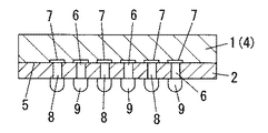
また、半導体装置は、上記のようにして調製した液状樹脂組成物を樹脂基板、セラミック基板又はウェハー等の各種部材1の表面に減圧印刷機を用いて塗布し、これを加熱硬化して樹脂層2を形成した後、図1に示すように、ダイシングソー3を用いてダイシング等により個片化する方法によって、製造することができる。このような製造方法によれば、反りが小さく、封止信頼性の高い半導体装置を安価な製造コストと短い製造タクトで得ることができ、液状樹脂組成物で形成される樹脂層2の内部にボイドを残存させないことができるものである。しかも、樹脂層2の内部には、多孔質あるいは中空の粒子からなる充填材が含有されていることによって、ダイシングソー3のブレードの磨耗を低減することができるものである。
Further, in the semiconductor device, the liquid resin composition prepared as described above is applied to the surface of
各種部材の表面に液状樹脂組成物を塗布する方法としては、真空印刷のほか、大気圧スクリーン印刷、スピンコーターによる塗布、あるいはディスペンスによる方法や、金型による成形法などを用いることができる。ただし、スピンコート法では粘度は溶剤の添加量を増やすなどして10Pa・s以下に押さえることが好ましく、金型による成形法では逆に溶剤を添加すると硬化物中にボイドが残る原因ともなるため溶剤を含まずに粘度を200Pa・s程度に押さえることが好ましい。樹脂層にボイドを内包しないための最良の方法は減圧印刷機を用いた方法であるが、この場合は溶剤の沸点を高沸点側にシフトするなどして連続印刷性を確保する必要がある。 As a method for applying the liquid resin composition to the surfaces of various members, vacuum printing, atmospheric pressure screen printing, application by a spin coater, dispensing method, molding method using a mold, or the like can be used. However, in the spin coating method, the viscosity is preferably suppressed to 10 Pa · s or less by increasing the amount of the solvent added. In the molding method using a mold, if a solvent is added on the contrary, voids may remain in the cured product. It is preferable to suppress the viscosity to about 200 Pa · s without containing a solvent. The best method for avoiding inclusion of voids in the resin layer is a method using a vacuum printer. In this case, it is necessary to ensure continuous printability by shifting the boiling point of the solvent to the high boiling point side.
また、印刷を用いた方法による場合は液状樹脂組成物の粘度は200Pa・s以下であることが好ましい。200Pa・sを超えると印刷対象への樹脂の転写が十分にされず、スキージングを繰り返す必要が生じるおそれがあるなどして好ましくない。また、溶剤を添加することで200Pa・s以下に抑えることができても添加量が10質量%を超える場合は硬化後に溶剤が残存して硬化物が脆くなってしまったり、多量の溶剤の揮発により硬化物中にボイドが生じたりするおそれがあるため好ましくない。硬化時の溶剤の揮発によるこのボイドを低減するには沸点の異なる溶剤を複数種添加して低沸点溶剤から順に緩やかに揮発させるのが一般的であるが特に真空印刷による方法ではこの限りではない。印刷時に低沸点溶剤が揮発して印刷中に粘度が上昇して連続して印刷する際に品質バラツキが発生しやすい。また硬化温度上限より溶剤の沸点が50〜100℃高ければ急激な揮発が押さえられ、徐々に溶剤が揮発するためボイドとなりにくく、硬化に要する時間に変更を加える必要もない。 In the case of a method using printing, the viscosity of the liquid resin composition is preferably 200 Pa · s or less. If it exceeds 200 Pa · s, the transfer of the resin to the printing object is not sufficient, and it may be necessary to repeat squeezing. Moreover, even if it can be suppressed to 200 Pa · s or less by adding a solvent, if the addition amount exceeds 10% by mass, the solvent remains after curing and the cured product becomes brittle, or a large amount of solvent volatilizes. This is not preferable because voids may occur in the cured product. In order to reduce this void due to solvent volatilization during curing, it is common to add multiple types of solvents with different boiling points and gradually evaporate in order from the low boiling point solvent, but this is not particularly the case with methods using vacuum printing. . The low boiling point solvent volatilizes during printing, and the viscosity increases during printing, so that quality variations are likely to occur when printing is performed continuously. Further, if the boiling point of the solvent is 50 to 100 ° C. higher than the upper limit of the curing temperature, rapid volatilization is suppressed, and since the solvent is gradually volatilized, it is difficult to form voids, and there is no need to change the time required for curing.
また、図2に示すように、シリコンチップ等の半導体チップ4の半導体回路側の面5には樹脂層2が配置され、かつ半導体チップ4に接続された多数の電極6がその樹脂層2を貫通して配置された型式の半導体装置において、半導体チップ4の半導体回路側の面5に配置されている樹脂層2を形成するために、液状樹脂組成物を好適に使用することができる。この形態の半導体装置は、一般にはCSP(チップスケールパッケージあるいはチップサイズパッケージ)と呼ばれる範疇のものであり、半導体チップ4を個片化する以前のシリコンウェハーの段階でCSPへの加工を行うことからWL(ウェハーレベル)あるいはWS(ウェハースケール)のCSPと呼ばれ、WL−CSP、WS−CSPと略されているものである。
As shown in FIG. 2, the
液状樹脂組成物を使用して、WL−CSPを製造するには、まず、CSPとなったときにバンプが形成される位置にあるウェハー上のパッド部7に、樹脂層2を貫通することになるポスト8としての金属を形成する。ポスト8を形成する方法としては、具体的には、パッド部7にフラックスを印刷し、その上にメタルマスクを利用して半田ボールを載せてリフローする方法や、パッド部7にハンダペーストを印刷してリフローする方法、あるいはパッド部7に銅などの金属をメッキ法により成長させる方法などがある。次に、ポスト8としての金属が形成されたウェハーに、液状樹脂組成物を印刷し、加熱硬化させる。印刷は減圧印刷によることが好ましい。常圧印刷の場合は、印刷後に減圧下に置いて、組成物中のボイドを除く処理を行うのが好ましい。加熱硬化は、常圧でも加圧下でも良いが、加圧下の方が硬化物中のボイドをより少なくすることができる。また硬化条件は、80〜140℃で30分〜2時間の1段目硬化を行った後に、150〜210℃で1〜6時間の2段目硬化を行うという2ステップ硬化を例示できる。フェノール性水酸基を有する化合物を硬化剤として使用した場合は、このような2ステップ硬化以外にも、100〜210℃で30分〜6時間の1ステップ硬化を採用することもできる。
In order to manufacture WL-CSP using a liquid resin composition, first, the
次に、液状樹脂組成物の硬化後のウェハーを樹脂層2側から研磨し、ポスト8と樹脂層2の高さを揃える。必要に応じて、その後にウェハーの背面を研磨し、総厚みを小さくする工程を採ることもある。
Next, the wafer after curing of the liquid resin composition is polished from the
研磨後のウェハーは、液状樹脂組成物の硬化物が適切なTgや弾性率、線膨張係数を有していることにより、例えば、8インチ径250μm厚のウェハーに50μm厚の樹脂層2を有する場合で1mm以下の反りとなるような小さな反りを実現でき、またリフロー後の反り量についても1mm以下に抑えることが可能となる。
The polished wafer has a
また、半導体チップ4の背面保護やマーキング性向上のため、ウェハーの背面に液状樹脂組成物あるいは、他の樹脂を塗布、硬化しても良い。
Further, in order to protect the back surface of the
次に、半田等を用いてCSPのバンプの形成を行う。具体的には、樹脂層2の表面に露出するポスト8の端面にフラックスを印刷し、その上にメタルマスクを利用して半田ボールを載せてリフローする方法や、ポスト8にハンダペーストを印刷してリフローする方法などがある。
Next, CSP bumps are formed using solder or the like. Specifically, a flux is printed on the end face of the
このようにして得られたウェハーをダイシングにより個片化すると、ポスト8とバンプ9からなる金属製の電極6を備えたCSPを得ることができる。このCSPは、密着性が良く、線膨張係数も適切なエポキシ樹脂組成物が使用されているので、また反りが小さいため内部応力が低いので、温度サイクル性や耐湿信頼性に優れているものである。
When the wafer thus obtained is separated into pieces by dicing, a CSP provided with
すなわち、上記のようにして形成された半導体装置にあっては、上述した液状樹脂組成物の硬化物により樹脂層が形成されているので、半導体装置としての反りを小さくすることができ、内部応力が低くなって優れた温度サイクル性や耐湿信頼性を実現することができると共に、リフロー時の熱履歴による反り量を低減することができるものである。 That is, in the semiconductor device formed as described above, since the resin layer is formed by the cured product of the liquid resin composition described above, warpage as a semiconductor device can be reduced, and internal stress can be reduced. As a result, the temperature cycle performance and moisture resistance reliability can be reduced, and the amount of warpage due to the heat history during reflow can be reduced.
以下、本発明を実施例によって具体的に説明する。 Hereinafter, the present invention will be specifically described by way of examples.
(実施例1〜5及び比較例1〜3)
下記[表1]に示す原材料の配合量(単位は質量部)及び製造法で、実施例1〜5及び比較例1〜3の液状樹脂組成物を調製した。
(Examples 1-5 and Comparative Examples 1-3)
The liquid resin compositions of Examples 1 to 5 and Comparative Examples 1 to 3 were prepared using the blending amounts of raw materials shown in [Table 1] below (unit: parts by mass) and production methods.
ここで、下記[表1]において使用した原材料は次のものである。 Here, the raw materials used in the following [Table 1] are as follows.
(充填材)
非晶質シリカ(MRCユニテック株式会社製、品番「QS9」、平均粒径9μm、最大粒径35μm)
非晶質シリカ(株式会社アドマテック製、品番「SO25H」、平均粒径0.6μm、最大粒径3.5μm)
中空シリカ(球状非晶質シリカ、平均粒径3μm、最大粒径25μm、空隙体積率50%)
多孔質シリカ(球状非晶質シリカ、焼成処理により表面密閉、平均粒径10μm、最大粒径30μm、空隙体積率20%)
多孔質シリカ(球状非晶質シリカ、焼成処理により表面密閉、平均粒径2μm、最大粒径25μm、空隙体積率17%)
多孔質シリカ(球状非晶質シリカ、平均粒径6μm、最大粒径30μm、空隙体積率33%)
(エポキシ樹脂)
ビスフェノールF型エポキシ樹脂(東都化成工業株式会社製、品番「YDF8170」、エポキシ当量160)
ビスフェノールA型エポキシ樹脂(東都化成工業株式会社製、品番「YD8125」、エポキシ当量175)
脂環式エポキシ樹脂(ダイセル化学工業株式会社製、品番「CEL2021」、エポキシ当量135)
ナフタレン環含有エポキシ樹脂(大日本インキ化学工業株式会社製、品番「HP4032D」、エポキシ当量141)
ポリプロピレン骨格含有エポキシ樹脂(東都化成株式会社製、品番「PG207GS」、エポキシ当量319)
(硬化剤)
アリル化フェノール(明和化成株式会社製、品番「MEH8000H」、水酸基当量141)
酸無水物(大日本インキ化学工業株式会社製、品番「B650」、酸無水物当量168)
(低弾性化剤)
シリコーンゴム
(溶剤)
ジエチレングリコールジエチルエーテル(沸点180℃)
ジメチルプロピレンジグリコール(沸点170℃)
ジブチルジグリコール(沸点250℃)
(硬化促進剤)
マイクロカプセル型潜在性硬化促進剤(旭化成工業株式会社製、品番「HXA3792」)
(着色剤)
カーボンブラック(三菱化学株式会社製、品番「MA100」)
その他にカップリング剤と分散剤を用いた。
(Filler)
Amorphous silica (MRC Unitech Co., Ltd., product number “QS9”,
Amorphous silica (manufactured by Admatech Co., Ltd., product number “SO25H”, average particle size 0.6 μm, maximum particle size 3.5 μm)
Hollow silica (spherical amorphous silica,
Porous silica (spherical amorphous silica, sealed by firing,
Porous silica (spherical amorphous silica, sealed by firing,
Porous silica (spherical amorphous silica,
(Epoxy resin)
Bisphenol F type epoxy resin (manufactured by Tohto Kasei Kogyo Co., Ltd., product number “YDF8170”, epoxy equivalent 160)
Bisphenol A type epoxy resin (manufactured by Toto Kasei Kogyo Co., Ltd., product number “YD8125”, epoxy equivalent 175)
Alicyclic epoxy resin (manufactured by Daicel Chemical Industries, product number “CEL2021”, epoxy equivalent 135)
Naphthalene ring-containing epoxy resin (Dainippon Ink Chemical Co., Ltd., product number “HP4032D”, epoxy equivalent 141)
Polypropylene skeleton-containing epoxy resin (manufactured by Toto Kasei Co., Ltd., product number “PG207GS”, epoxy equivalent 319)
(Curing agent)
Allylated phenol (Maywa Kasei Co., Ltd., product number “MEH8000H”, hydroxyl group equivalent 141)
Acid anhydride (manufactured by Dainippon Ink and Chemicals, product number “B650”, acid anhydride equivalent 168)
(Low elasticity agent)
Silicone rubber (solvent)
Diethylene glycol diethyl ether (boiling point 180 ° C)
Dimethylpropylene diglycol (boiling point 170 ° C)
Dibutyl diglycol (boiling point 250 ° C)
(Curing accelerator)
Microcapsule type latent curing accelerator (manufactured by Asahi Kasei Corporation, product number “HXA3792”)
(Coloring agent)
Carbon black (Mitsubishi Chemical Corporation, part number “MA100”)
In addition, a coupling agent and a dispersant were used.
また、下記[表1]において採用した製造方法は次の通りである。 Moreover, the manufacturing method employ | adopted in the following [Table 1] is as follows.
(製造方法A)
液状樹脂組成物の構成成分である充填材、エポキシ樹脂、硬化剤、その他の成分を下記[表1]に示す配合量で配合し、これをホモディスパー(特殊機化工業製)にて300〜500rpmの条件で分散・混合することによって、液状樹脂組成物を調製した。
(Production method A)
The filler, epoxy resin, curing agent, and other components that are constituents of the liquid resin composition are blended in the blending amounts shown in [Table 1] below, and this is 300 to 300 by homodisper (made by Tokushu Kika Kogyo Co., Ltd.). A liquid resin composition was prepared by dispersing and mixing at 500 rpm.
(製造方法B)
液状樹脂組成物の構成成分である充填材、エポキシ樹脂、硬化剤、その他の成分を下記[表1]に示す配合量で配合し、これをプラネタリーミキサーで混合し、さらに3本ロールにて分散することによって、液状樹脂組成物を調製した。
(Production method B)
The filler, epoxy resin, curing agent, and other components that are constituents of the liquid resin composition are blended in the blending amounts shown in [Table 1] below, mixed with a planetary mixer, and further mixed with three rolls. A liquid resin composition was prepared by dispersing.
(製造方法C)
液状樹脂組成物の構成成分であるエポキシ樹脂、硬化剤、その他の成分(多孔質・中空の充填材を除く)を下記[表1]に示す配合量で配合し、これをプラネタリーミキサーで混合し、さらに3本ロールにて分散した後に多孔質・中空の充填材を添加してプラネタリーミキサーによって再度攪拌することによって、液状樹脂組成物を調製した。
(Manufacturing method C)
The epoxy resin, curing agent, and other components (excluding porous and hollow fillers), which are constituents of the liquid resin composition, are blended in the blending amounts shown in [Table 1] below, and mixed with a planetary mixer. Further, after being dispersed by three rolls, a porous / hollow filler was added and stirred again by a planetary mixer to prepare a liquid resin composition.
実施例1〜5及び比較例1〜3で得られた液状樹脂組成物の特性を次の方法で測定した。測定結果を下記[表1]に示す。 The characteristics of the liquid resin compositions obtained in Examples 1 to 5 and Comparative Examples 1 to 3 were measured by the following method. The measurement results are shown in [Table 1] below.
(1)加工条件
図1に示すように、部材1(200μm厚ウェハー)の表面に液状樹脂組成物を塗布・加熱して200μm厚の樹脂層2を形成し、ダイシングソー3を用いて個片化する際のブレードの磨耗量及びスピンドル電流値を測定した。使用装置、使用ブレード、加工条件は次の通りである。
(1) Processing conditions As shown in FIG. 1, a liquid resin composition is applied to the surface of a member 1 (200 μm thick wafer) and heated to form a 200 μm
使用装置
ディスコ社製「DFD6340 FULLY AUTOMATIC DICING SAW」
使用ブレード
「NBC−ZH2050」
加工条件
スピンドル回転数:35000rpm、送り速度:50mm/s、切削水:純粋、加工距離:9.8m
(2)液状樹脂組成物の粘度
室温(25℃)にてB型粘度計を用いて測定した。
Equipment used "DFD6340 FULL AUTOMATIC DICING SAW" manufactured by DISCO
Used blade "NBC-ZH2050"
Processing conditions Spindle rotation speed: 35000 rpm, feed rate: 50 mm / s, cutting water: pure, processing distance: 9.8 m
(2) Viscosity of liquid resin composition Measured using a B-type viscometer at room temperature (25 ° C).
(3)ガラス転移温度(Tg)
粘弾性スペクトロメータ(DMA)の曲げモード10Hzにて評価した。試験片は、液状樹脂組成物を130℃で1時間加熱した後、180℃で3時間加熱して形成したものであって、5mm幅×50mm長×0.2mm厚に切り出したものを用いた。昇温は2℃/分により−60℃〜260℃まで測定した。
(3) Glass transition temperature (Tg)
Evaluation was made at a bending mode of 10 Hz of a viscoelastic spectrometer (DMA). The test piece was formed by heating the liquid resin composition at 130 ° C. for 1 hour and then heating at 180 ° C. for 3 hours, and was cut into 5 mm width × 50 mm length × 0.2 mm thickness. . The temperature rise was measured from −60 ° C. to 260 ° C. at 2 ° C./min.
(4)線膨張率
熱分析計TMAにより評価した。液状樹脂組成物を硬化させて、70mm以上長×10mm幅×1〜3mm厚の試験片を形成し、この試験片を用いて昇温速度5℃/分により−60℃〜260℃まで測定した。液状樹脂組成物の硬化は130℃で1時間加熱した後、180℃で3時間加熱して行った。
( 4 ) Linear expansion coefficient It evaluated by the thermal analyzer TMA. The liquid resin composition was cured to form a test piece having a length of 70 mm or longer, a width of 10 mm, and a thickness of 1 to 3 mm, and the test piece was measured from −60 ° C. to 260 ° C. at a heating rate of 5 ° C./min. . The liquid resin composition was cured by heating at 130 ° C. for 1 hour and then heating at 180 ° C. for 3 hours.
(5)反り
5インチで200μm厚のウェハーの表面に液状樹脂組成物を直径110mmで0.2μm厚に塗布し、130℃で1時間加熱した後、180℃で3時間加熱することによって、硬化させた。液状樹脂組成物の硬化後、円周端部の一点を押さえ垂直方向(Z軸方向)に反り上がった最大値を測定することにより反り量を評価した。
( 5 ) Warpage Cured by applying a liquid resin composition to a surface of a 5-inch wafer having a thickness of 200 μm to a thickness of 110 μm and a thickness of 0.2 μm, heating at 130 ° C. for 1 hour, and then heating at 180 ° C. for 3 hours. I let you. After the liquid resin composition was cured, the amount of warpage was evaluated by measuring a maximum value obtained by warping in the vertical direction (Z-axis direction) while pressing one point on the circumferential edge.
(6)樹脂硬度
JISK5600に基づいて引掻き硬度試験機による鉛筆法にて評価した。試験片は、液状樹脂組成物を硬化させて、70mm以上長×10mm幅×3mm厚に形成したものを用い、引掻き硬度試験機により鉛筆を押し付けて塗膜硬度を測定した。
( 6 ) Resin hardness Based on JISK5600, it evaluated by the pencil method by a scratch hardness tester. The test piece was prepared by curing the liquid resin composition and forming a length of 70 mm or more, length x 10 mm width x 3 mm, and measuring the coating film hardness by pressing a pencil with a scratch hardness tester.
(7)PCT
図1に示すように、部材1(ウェハー)の表面に液状樹脂組成物を塗布・加熱して樹脂層2を形成し、ダイシングソー3を用いて個片化することによって、樹脂付きウェハーチップ(大きさ:5mm×5mm、樹脂層2の厚み:200μm厚、部材1(ウェハー)の厚み:200μm厚)を作製した。なお、使用装置、使用ブレード、加工条件は(1)と同じである。
( 7 ) PCT
As shown in FIG. 1, a
上記のようにして個片化した樹脂付きウェハーチップを121℃、2atm(0.20MPa)のPCT条件にて300時間処理した。その後、樹脂硬度を鉛筆法による引掻きモードで評価した。 The resin-coated wafer chip singulated as described above was treated for 300 hours under PCT conditions of 121 ° C. and 2 atm (0.20 MPa). Thereafter, the resin hardness was evaluated in a scratch mode by a pencil method.
(8)TS信頼性
温度サイクル性を評価するためのサンプルとして、(7)で用いたのと同じ樹脂付きウェハーチップを10個ずつ用いた。これらのサンプルに−65℃で5分間、150℃で5分間を1サイクルとする液相の温度サイクルを与え、1000サイクルまで100サイクルごとに樹脂層の剥離確認を行い、良否を判定した。10個のサンプルのうち不良の数が5個に達したときのサイクル数を求めた。
( 8 ) TS reliability Ten samples of resin-coated wafer chips used in ( 7 ) were used as samples for evaluating temperature cycle performance. These samples were given a liquid phase temperature cycle of 1 cycle of -65 ° C. for 5 minutes and 150 ° C. for 5 minutes, and peeling of the resin layer was confirmed every 100 cycles up to 1000 cycles to determine pass / fail. The number of cycles when the number of defects reached 5 out of 10 samples was determined.
(9)耐リフロー性評価
(7)で用いたのと同じ樹脂付きウェハーチップ10個について、85℃、85%RHにて吸湿処理後、ピーク温度263℃のリフロー炉により2回処理し、樹脂層の剥離状態を超音波検査装置にて確認した。
( 9 ) Evaluation of reflow resistance Ten resin-coated wafer chips used in ( 7 ) were subjected to moisture absorption treatment at 85 ° C. and 85% RH, and then treated twice in a reflow furnace having a peak temperature of 263 ° C. The peeling state of the layer was confirmed with an ultrasonic inspection apparatus.

上記[表1]にみられるように、実施例1では中空シリカにより優れた低磨耗特性と低反り、各種信頼性が実現されていることが確認される。 As seen in [Table 1] above, in Example 1, it is confirmed that the hollow silica has excellent low wear characteristics, low warpage, and various reliability.
また、実施例2においては、実施例1の中空シリカの一部を多孔質シリカに置き替えているが、同様に低磨耗性と低反り、高信頼性を実現しながら粘度及びチクソ性を低く抑える効果が確認できる。 Further, in Example 2, a part of the hollow silica of Example 1 is replaced with porous silica. Similarly, the low viscosity and thixotropy are achieved while realizing low wear and warpage, and high reliability. The suppression effect can be confirmed.
また、実施例3においてはエラストマー量を最小限に抑えることで樹脂硬度が向上している。 In Example 3, the resin hardness is improved by minimizing the amount of elastomer.
また、実施例4では多孔質・中空ではないシリカを用いずにすべて多孔質シリカを用いることによりブレードの磨耗量を極小化する効果がみられる。 In Example 4, the effect of minimizing the amount of wear of the blade can be seen by using all porous silica without using porous or non-hollow silica.
また、実施例5ではブレードの磨耗量は少ないものの、多孔質シリカの表面が密閉されていないため樹脂の粘度やチクソ指数が上昇し、他の実施例に比べてあまり好ましくない。また、硬度や反りの点でも他の実施例に比べて劣っている。 Further, in Example 5, although the blade wear amount is small, the viscosity of the resin and the thixo index increase because the surface of the porous silica is not sealed, which is not preferable compared to other examples. Also, the hardness and warpage are inferior to those of the other examples.
一方、比較例1では樹脂のTgが比較的低く、反りは低いが樹脂硬度が十分ではない。また、比較例2では充填材の充填量が少ないため、線膨張率が大きく、反りの増大が著しい。また、比較例3では硬化剤として酸無水物を使用しているためPCT後の樹脂硬度の低下が著しい。 On the other hand, in Comparative Example 1, the resin has a relatively low Tg and low warpage, but the resin hardness is not sufficient. In Comparative Example 2, since the filling amount of the filler is small, the linear expansion coefficient is large, and the warpage is remarkably increased. Moreover, since the acid anhydride is used as a hardening | curing agent in the comparative example 3, the fall of the resin hardness after PCT is remarkable.
2 樹脂層
4 半導体チップ
5 半導体回路側の面
6 電極
2
Claims (11)
Priority Applications (2)
| Application Number | Priority Date | Filing Date | Title |
|---|---|---|---|
| JP2006343323A JP5270833B2 (en) | 2006-12-20 | 2006-12-20 | Liquid resin composition, semiconductor device and manufacturing method thereof |
| US12/435,639 US8106523B2 (en) | 2006-12-20 | 2009-05-05 | Liquid resin composition, semi-conductor device, and process of fabricating the same |
Applications Claiming Priority (1)
| Application Number | Priority Date | Filing Date | Title |
|---|---|---|---|
| JP2006343323A JP5270833B2 (en) | 2006-12-20 | 2006-12-20 | Liquid resin composition, semiconductor device and manufacturing method thereof |
Publications (3)
| Publication Number | Publication Date |
|---|---|
| JP2008156383A JP2008156383A (en) | 2008-07-10 |
| JP2008156383A5 JP2008156383A5 (en) | 2009-07-23 |
| JP5270833B2 true JP5270833B2 (en) | 2013-08-21 |
Family
ID=39657680
Family Applications (1)
| Application Number | Title | Priority Date | Filing Date |
|---|---|---|---|
| JP2006343323A Active JP5270833B2 (en) | 2006-12-20 | 2006-12-20 | Liquid resin composition, semiconductor device and manufacturing method thereof |
Country Status (2)
| Country | Link |
|---|---|
| US (1) | US8106523B2 (en) |
| JP (1) | JP5270833B2 (en) |
Families Citing this family (15)
| Publication number | Priority date | Publication date | Assignee | Title |
|---|---|---|---|---|
| JP5574237B2 (en) * | 2008-05-21 | 2014-08-20 | ナガセケムテックス株式会社 | Epoxy resin composition for sealing electronic parts |
| JP5259500B2 (en) * | 2009-06-10 | 2013-08-07 | 電気化学工業株式会社 | Amorphous siliceous powder and its production method and application |
| JP5672589B2 (en) * | 2009-06-25 | 2015-02-18 | パナソニックIpマネジメント株式会社 | Liquid epoxy resin composition |
| EP2825605B1 (en) * | 2012-04-24 | 2017-03-15 | Dow Global Technologies LLC | Epoxy resin composition for marine maintenance and repair coatings with improved overcoat ability |
| WO2013159277A1 (en) | 2012-04-24 | 2013-10-31 | Dow Global Technologies Llc | Epoxy resin composition for marine maintenance and repair coatings with improved overcoatability |
| US8980026B2 (en) | 2012-09-28 | 2015-03-17 | Apple Inc. | Gap seals for electronic device structures |
| JP6185342B2 (en) * | 2013-09-05 | 2017-08-23 | 信越化学工業株式会社 | Encapsulant laminated composite, post-sealing semiconductor element mounting substrate or post-sealing semiconductor element forming wafer, and method for manufacturing semiconductor device |
| CN106133054B (en) * | 2014-03-25 | 2017-07-28 | 松下知识产权经营株式会社 | Liquid resin composition, solidfied material, wiring structural body and the assembly using the wiring structural body |
| WO2016044179A2 (en) * | 2014-09-15 | 2016-03-24 | Invensas Corporation | Electronic structures strengthened by porous and non-porous layers, and methods of fabrication |
| WO2016125664A1 (en) * | 2015-02-05 | 2016-08-11 | 味の素株式会社 | Resin composition |
| KR20170053416A (en) * | 2015-11-06 | 2017-05-16 | 주식회사 엘지화학 | Semiconductor device and manufacturing method of the same |
| JP6901327B2 (en) * | 2017-06-12 | 2021-07-14 | 株式会社フジミインコーポレーテッド | Fillers, moldings, and heat dissipation materials |
| WO2019003600A1 (en) * | 2017-06-28 | 2019-01-03 | 京セラ株式会社 | Sealing resin composition, electronic component, and electronic component manufacturing method |
| WO2020133494A1 (en) * | 2018-12-29 | 2020-07-02 | 广东生益科技股份有限公司 | Resin composition, prepreg, laminated board, metal foil-clad laminated board, and printed circuit board |
| CN118159606A (en) * | 2021-11-17 | 2024-06-07 | 三键有限公司 | Microcapsule-type curable resin composition |
Family Cites Families (16)
| Publication number | Priority date | Publication date | Assignee | Title |
|---|---|---|---|---|
| US4111713A (en) * | 1975-01-29 | 1978-09-05 | Minnesota Mining And Manufacturing Company | Hollow spheres |
| JPS58138728A (en) * | 1982-02-15 | 1983-08-17 | Matsushita Electric Works Ltd | Epoxy resin composition |
| CA2087911C (en) * | 1992-01-24 | 1999-06-29 | Kiyoshi Abe | Spherical granules of porous silica or silicate, process for the production thereof, and applications thereof |
| JP3143220B2 (en) * | 1992-07-07 | 2001-03-07 | 電気化学工業株式会社 | Filler and resin composition for semiconductor encapsulation using the same |
| JP3454554B2 (en) * | 1993-12-28 | 2003-10-06 | 水澤化学工業株式会社 | Amorphous silica granules and production method thereof |
| JPH0885719A (en) * | 1994-07-19 | 1996-04-02 | Matsushita Electric Works Ltd | Liquid epoxy resin composition and its production |
| JPH0841173A (en) * | 1994-07-27 | 1996-02-13 | Matsushita Electric Works Ltd | Liquid epoxy resin composition, its production and method of curing same |
| JP3119104B2 (en) * | 1994-12-09 | 2000-12-18 | 信越化学工業株式会社 | Epoxy resin composition |
| JP4614214B2 (en) * | 1999-12-02 | 2011-01-19 | 信越化学工業株式会社 | Hollow package for semiconductor device elements |
| JP2001181479A (en) * | 1999-12-27 | 2001-07-03 | Matsushita Electric Works Ltd | Epoxy resin composition for sealing and semiconductor devices |
| JP2002338230A (en) * | 2001-05-22 | 2002-11-27 | Toagosei Co Ltd | Silica particles and resin composition |
| JP3794349B2 (en) * | 2002-06-25 | 2006-07-05 | 松下電工株式会社 | Liquid epoxy resin composition for sealing and semiconductor device |
| JP2005264037A (en) * | 2004-03-19 | 2005-09-29 | Kyocera Chemical Corp | Epoxy resin composition for sealing and resin-sealed semiconductor device |
| JP4112540B2 (en) * | 2004-08-26 | 2008-07-02 | 電気化学工業株式会社 | Manufacturing method of spherical inorganic hollow powder. |
| JP2006232950A (en) | 2005-02-23 | 2006-09-07 | Matsushita Electric Works Ltd | Sealing liquid epoxy resin composition, semiconductor device, and method for producing the same |
| JP2006233016A (en) * | 2005-02-24 | 2006-09-07 | Sumitomo Bakelite Co Ltd | Epoxy resin composition and semiconductor device |
-
2006
- 2006-12-20 JP JP2006343323A patent/JP5270833B2/en active Active
-
2009
- 2009-05-05 US US12/435,639 patent/US8106523B2/en active Active
Also Published As
| Publication number | Publication date |
|---|---|
| US8106523B2 (en) | 2012-01-31 |
| JP2008156383A (en) | 2008-07-10 |
| US20090261484A1 (en) | 2009-10-22 |
Similar Documents
| Publication | Publication Date | Title |
|---|---|---|
| JP5270833B2 (en) | Liquid resin composition, semiconductor device and manufacturing method thereof | |
| JP5354753B2 (en) | Underfill material and semiconductor device | |
| JP2006232950A (en) | Sealing liquid epoxy resin composition, semiconductor device, and method for producing the same | |
| JP7513074B2 (en) | Encapsulating resin composition, electronic component device, and method for producing electronic component device | |
| KR20120092505A (en) | Semiconductor-encapsulating liquid epoxy resin composition and semiconductor device | |
| JP3794349B2 (en) | Liquid epoxy resin composition for sealing and semiconductor device | |
| JP5672589B2 (en) | Liquid epoxy resin composition | |
| JP7210031B2 (en) | Film semiconductor sealing material | |
| KR102399157B1 (en) | Film adhesive and semiconductor device using same | |
| WO2011129272A1 (en) | Attachment material for semiconductor chip bonding, attachment film for semiconductor chip bonding, semiconductor device manufacturing method, and semiconductor device | |
| TWI480326B (en) | Curable resin compositions useful as underfill sealants for low-k dielectric-containing semiconductor devices | |
| WO2015104917A1 (en) | Liquid epoxy resin composition for semiconductor sealing and resin-sealed semiconductor device | |
| KR101245414B1 (en) | Liquid epoxy resin composition | |
| JP7167912B2 (en) | Liquid encapsulating resin composition, electronic component device, and method for manufacturing electronic component device | |
| JP6115929B2 (en) | Epoxy resin composition | |
| JP2003128874A (en) | Liquid resin composition, manufacturing method of semiconductor device and semiconductor device | |
| JP2019151713A (en) | Film-like semiconductor encapsulation material | |
| JP2006016431A (en) | Liquid epoxy resin composition for semiconductor sealing and flip chip type semiconductor | |
| JP2003192767A (en) | Liquid resin composition, method for manufacturing semiconductor device and semiconductor device | |
| JP7509192B2 (en) | Encapsulating resin composition, electronic component device, and method for producing electronic component device | |
| JP2013107993A (en) | Liquid resin composition for semiconductor sealing and semiconductor device using the same | |
| JP6920723B2 (en) | NCF for pressure mounting | |
| JP5532582B2 (en) | Method for sealing flip-chip type semiconductor device, method for selecting chip-on-chip underfill material, and flip-chip type semiconductor device | |
| TWI811215B (en) | Sealing resin composition, electronic component apparatus and manufacturing method for electronic component apparatus | |
| JP2004067930A (en) | Liquid encapsulation resin composition, semiconductor device using same and manufacturing process of the semiconductor device |
Legal Events
| Date | Code | Title | Description |
|---|---|---|---|
| A621 | Written request for application examination |
Free format text: JAPANESE INTERMEDIATE CODE: A621 Effective date: 20081028 |
|
| A521 | Written amendment |
Free format text: JAPANESE INTERMEDIATE CODE: A523 Effective date: 20090609 |
|
| RD04 | Notification of resignation of power of attorney |
Free format text: JAPANESE INTERMEDIATE CODE: A7424 Effective date: 20100902 |
|
| A977 | Report on retrieval |
Free format text: JAPANESE INTERMEDIATE CODE: A971007 Effective date: 20110603 |
|
| A131 | Notification of reasons for refusal |
Free format text: JAPANESE INTERMEDIATE CODE: A131 Effective date: 20110607 |
|
| A521 | Written amendment |
Free format text: JAPANESE INTERMEDIATE CODE: A523 Effective date: 20110808 |
|
| A02 | Decision of refusal |
Free format text: JAPANESE INTERMEDIATE CODE: A02 Effective date: 20110920 |
|
| A521 | Written amendment |
Free format text: JAPANESE INTERMEDIATE CODE: A523 Effective date: 20111205 |
|
| A911 | Transfer to examiner for re-examination before appeal (zenchi) |
Free format text: JAPANESE INTERMEDIATE CODE: A911 Effective date: 20111219 |
|
| A711 | Notification of change in applicant |
Free format text: JAPANESE INTERMEDIATE CODE: A712 Effective date: 20120111 |
|
| A131 | Notification of reasons for refusal |
Free format text: JAPANESE INTERMEDIATE CODE: A131 Effective date: 20120306 |
|
| A521 | Written amendment |
Free format text: JAPANESE INTERMEDIATE CODE: A523 Effective date: 20120507 |
|
| A912 | Re-examination (zenchi) completed and case transferred to appeal board |
Free format text: JAPANESE INTERMEDIATE CODE: A912 Effective date: 20120831 |
|
| A61 | First payment of annual fees (during grant procedure) |
Free format text: JAPANESE INTERMEDIATE CODE: A61 Effective date: 20130510 |
|
| R150 | Certificate of patent or registration of utility model |
Free format text: JAPANESE INTERMEDIATE CODE: R150 Ref document number: 5270833 Country of ref document: JP Free format text: JAPANESE INTERMEDIATE CODE: R150 |