JP5207451B2 - 放射線画像検出器 - Google Patents
放射線画像検出器 Download PDFInfo
- Publication number
- JP5207451B2 JP5207451B2 JP2008070925A JP2008070925A JP5207451B2 JP 5207451 B2 JP5207451 B2 JP 5207451B2 JP 2008070925 A JP2008070925 A JP 2008070925A JP 2008070925 A JP2008070925 A JP 2008070925A JP 5207451 B2 JP5207451 B2 JP 5207451B2
- Authority
- JP
- Japan
- Prior art keywords
- layer
- radiation
- image detector
- electrode
- hole injection
- Prior art date
- Legal status (The legal status is an assumption and is not a legal conclusion. Google has not performed a legal analysis and makes no representation as to the accuracy of the status listed.)
- Active
Links
- 230000005855 radiation Effects 0.000 title claims description 132
- 238000002347 injection Methods 0.000 claims description 77
- 239000007924 injection Substances 0.000 claims description 77
- 230000000903 blocking effect Effects 0.000 claims description 57
- 239000004065 semiconductor Substances 0.000 claims description 39
- 238000002425 crystallisation Methods 0.000 claims description 26
- 230000008025 crystallization Effects 0.000 claims description 22
- 229910052711 selenium Inorganic materials 0.000 claims description 17
- 229910052785 arsenic Inorganic materials 0.000 claims description 9
- 239000000956 alloy Substances 0.000 claims description 8
- 229910045601 alloy Inorganic materials 0.000 claims description 8
- 239000011669 selenium Substances 0.000 description 34
- 238000003860 storage Methods 0.000 description 20
- 239000000758 substrate Substances 0.000 description 17
- 206010047571 Visual impairment Diseases 0.000 description 12
- 239000011159 matrix material Substances 0.000 description 12
- 239000000203 mixture Substances 0.000 description 11
- 239000003990 capacitor Substances 0.000 description 10
- 230000000694 effects Effects 0.000 description 9
- 239000000463 material Substances 0.000 description 8
- 230000002265 prevention Effects 0.000 description 8
- BUGBHKTXTAQXES-UHFFFAOYSA-N Selenium Chemical compound [Se] BUGBHKTXTAQXES-UHFFFAOYSA-N 0.000 description 7
- 239000013078 crystal Substances 0.000 description 6
- 230000007547 defect Effects 0.000 description 6
- 238000000151 deposition Methods 0.000 description 6
- 239000002994 raw material Substances 0.000 description 6
- 239000004020 conductor Substances 0.000 description 5
- 230000003287 optical effect Effects 0.000 description 5
- 238000006243 chemical reaction Methods 0.000 description 4
- 230000008021 deposition Effects 0.000 description 4
- OAICVXFJPJFONN-UHFFFAOYSA-N Phosphorus Chemical compound [P] OAICVXFJPJFONN-UHFFFAOYSA-N 0.000 description 3
- 229910052782 aluminium Inorganic materials 0.000 description 3
- 238000001514 detection method Methods 0.000 description 3
- 239000011521 glass Substances 0.000 description 3
- 238000010438 heat treatment Methods 0.000 description 3
- 229920003227 poly(N-vinyl carbazole) Polymers 0.000 description 3
- 229910021417 amorphous silicon Inorganic materials 0.000 description 2
- 229910052787 antimony Inorganic materials 0.000 description 2
- 230000015572 biosynthetic process Effects 0.000 description 2
- 229910052804 chromium Inorganic materials 0.000 description 2
- 229910052737 gold Inorganic materials 0.000 description 2
- 239000012212 insulator Substances 0.000 description 2
- 238000004519 manufacturing process Methods 0.000 description 2
- 229910052751 metal Inorganic materials 0.000 description 2
- 239000002184 metal Substances 0.000 description 2
- 238000000034 method Methods 0.000 description 2
- 230000004048 modification Effects 0.000 description 2
- 238000012986 modification Methods 0.000 description 2
- IEQIEDJGQAUEQZ-UHFFFAOYSA-N phthalocyanine Chemical compound N1C(N=C2C3=CC=CC=C3C(N=C3C4=CC=CC=C4C(=N4)N3)=N2)=C(C=CC=C2)C2=C1N=C1C2=CC=CC=C2C4=N1 IEQIEDJGQAUEQZ-UHFFFAOYSA-N 0.000 description 2
- 229910052717 sulfur Inorganic materials 0.000 description 2
- 238000007740 vapor deposition Methods 0.000 description 2
- OGGKVJMNFFSDEV-UHFFFAOYSA-N 3-methyl-n-[4-[4-(n-(3-methylphenyl)anilino)phenyl]phenyl]-n-phenylaniline Chemical compound CC1=CC=CC(N(C=2C=CC=CC=2)C=2C=CC(=CC=2)C=2C=CC(=CC=2)N(C=2C=CC=CC=2)C=2C=C(C)C=CC=2)=C1 OGGKVJMNFFSDEV-UHFFFAOYSA-N 0.000 description 1
- RZVAJINKPMORJF-UHFFFAOYSA-N Acetaminophen Chemical compound CC(=O)NC1=CC=C(O)C=C1 RZVAJINKPMORJF-UHFFFAOYSA-N 0.000 description 1
- 239000004985 Discotic Liquid Crystal Substance Substances 0.000 description 1
- FYYHWMGAXLPEAU-UHFFFAOYSA-N Magnesium Chemical compound [Mg] FYYHWMGAXLPEAU-UHFFFAOYSA-N 0.000 description 1
- 239000004793 Polystyrene Substances 0.000 description 1
- 229910018110 Se—Te Inorganic materials 0.000 description 1
- 229910006404 SnO 2 Inorganic materials 0.000 description 1
- 230000005540 biological transmission Effects 0.000 description 1
- 238000010549 co-Evaporation Methods 0.000 description 1
- XCJYREBRNVKWGJ-UHFFFAOYSA-N copper(II) phthalocyanine Chemical compound [Cu+2].C12=CC=CC=C2C(N=C2[N-]C(C3=CC=CC=C32)=N2)=NC1=NC([C]1C=CC=CC1=1)=NC=1N=C1[C]3C=CC=CC3=C2[N-]1 XCJYREBRNVKWGJ-UHFFFAOYSA-N 0.000 description 1
- 230000007423 decrease Effects 0.000 description 1
- 230000002950 deficient Effects 0.000 description 1
- 238000010586 diagram Methods 0.000 description 1
- 239000006185 dispersion Substances 0.000 description 1
- 238000011156 evaluation Methods 0.000 description 1
- 230000008020 evaporation Effects 0.000 description 1
- 238000001704 evaporation Methods 0.000 description 1
- 238000002474 experimental method Methods 0.000 description 1
- 229910052738 indium Inorganic materials 0.000 description 1
- APFVFJFRJDLVQX-UHFFFAOYSA-N indium atom Chemical compound [In] APFVFJFRJDLVQX-UHFFFAOYSA-N 0.000 description 1
- AMGQUBHHOARCQH-UHFFFAOYSA-N indium;oxotin Chemical compound [In].[Sn]=O AMGQUBHHOARCQH-UHFFFAOYSA-N 0.000 description 1
- 229910052749 magnesium Inorganic materials 0.000 description 1
- 239000011777 magnesium Substances 0.000 description 1
- 238000009607 mammography Methods 0.000 description 1
- 229910044991 metal oxide Inorganic materials 0.000 description 1
- 229910052750 molybdenum Inorganic materials 0.000 description 1
- 150000002894 organic compounds Chemical class 0.000 description 1
- YRZZLAGRKZIJJI-UHFFFAOYSA-N oxyvanadium phthalocyanine Chemical compound [V+2]=O.C12=CC=CC=C2C(N=C2[N-]C(C3=CC=CC=C32)=N2)=NC1=NC([C]1C=CC=CC1=1)=NC=1N=C1[C]3C=CC=CC3=C2[N-]1 YRZZLAGRKZIJJI-UHFFFAOYSA-N 0.000 description 1
- 239000012466 permeate Substances 0.000 description 1
- 239000004417 polycarbonate Substances 0.000 description 1
- 229920000515 polycarbonate Polymers 0.000 description 1
- 229920000642 polymer Polymers 0.000 description 1
- 229920002223 polystyrene Polymers 0.000 description 1
- 239000005297 pyrex Substances 0.000 description 1
- 239000000126 substance Substances 0.000 description 1
- 238000002207 thermal evaporation Methods 0.000 description 1
- 229910052721 tungsten Inorganic materials 0.000 description 1
- 238000001771 vacuum deposition Methods 0.000 description 1
- YVTHLONGBIQYBO-UHFFFAOYSA-N zinc indium(3+) oxygen(2-) Chemical compound [O--].[Zn++].[In+3] YVTHLONGBIQYBO-UHFFFAOYSA-N 0.000 description 1
Images


Description

2%〜15%であることが望ましい。
−Se層を薄くし、光透過型の第1の電極層を設けるとともに、第1の電極層の上方に蛍光体を設け、その蛍光体からの光を電荷に変換するものである。なお、上記のように構成された放射線画像検出器においては、記録用光導電層や半導体層の厚さは1〜30μm程度となり、TFT読取方式の放射線画像検出器の場合には、蓄積容量はなくてもよい。
2 正孔注入阻止層
3 記録用光導電層(半導体層)
4 電荷輸送層
5 読取用光導電層
6 蓄電部
7 第2の電極層
8 透明線状電極
9 遮光線状電極
10 放射線画像検出器
11 結晶化防止層
20 高圧電源
30 チャージアンプ
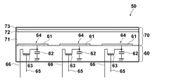
50 放射線画像検出器
55 電圧源
60 アクティブマトリクス基板
61 収集電極
62 蓄積容量
63 TFTスイッチ
64 画素
65 走査配線
66 データ配線
70 放射線検出部
71 半導体層
72 正孔注入阻止層
73 上部電極(電圧印加電極)
74 結晶化防止層
80 読出回路
90 ゲートドライバ
101 第1の電極層
102 記録用光導電層
103 電荷輸送層
104 読取用光導電層
105 蓄電部
106 透明線状電極
107 遮光線状電極
Claims (6)
- 電圧が印加される電圧印加電極と、放射線の照射を受けて電荷を発生する半導体層と、放射線量に応じた電気信号を検出する電極とが積層され、前記半導体層において発生した電荷に応じた画像信号が読み出される放射線画像検出器において、
前記電圧印加電極と前記半導体層との間に、前記電圧印加電極から前記半導体層への正孔の注入を阻止する正孔注入阻止層が設けられ、
該正孔注入阻止層がSbxS100−xの合金からなり、前記xが41≦x≦60を満たすものであることを特徴とする放射線画像検出器。 - 前記正孔注入阻止層の厚さが、0.25μm以上3μm以下であることを特徴とする請求項1記載の放射線画像検出器。
- 前記正孔注入阻止層と前記半導体層との間に、SeとAsとを主成分とする結晶化防止層が設けられていることを特徴とする請求項1または2記載の放射線画像検出器。
- 前記結晶化防止層におけるAsの成分が2%〜15%であることを特徴とする請求項3記載の放射線画像検出器。
- 前記電圧印加電極が、前記放射線の照射時には負電圧が印加され、前記画像信号の読出し時には接地されるものであることを特徴とする請求項1から4いずれか1項記載の放射線画像検出器。
- 前記電圧印加電極が、前記放射線の照射時には正の電圧が印加されるものであることを特徴とする請求項1から4いずれか1項記載の放射線画像検出器。
Priority Applications (2)
| Application Number | Priority Date | Filing Date | Title |
|---|---|---|---|
| JP2008070925A JP5207451B2 (ja) | 2007-09-28 | 2008-03-19 | 放射線画像検出器 |
| US12/240,299 US7608833B2 (en) | 2007-09-28 | 2008-09-29 | Radiation image detector |
Applications Claiming Priority (3)
| Application Number | Priority Date | Filing Date | Title |
|---|---|---|---|
| JP2007254604 | 2007-09-28 | ||
| JP2007254604 | 2007-09-28 | ||
| JP2008070925A JP5207451B2 (ja) | 2007-09-28 | 2008-03-19 | 放射線画像検出器 |
Publications (2)
| Publication Number | Publication Date |
|---|---|
| JP2009099933A JP2009099933A (ja) | 2009-05-07 |
| JP5207451B2 true JP5207451B2 (ja) | 2013-06-12 |
Family
ID=40702607
Family Applications (1)
| Application Number | Title | Priority Date | Filing Date |
|---|---|---|---|
| JP2008070925A Active JP5207451B2 (ja) | 2007-09-28 | 2008-03-19 | 放射線画像検出器 |
Country Status (1)
| Country | Link |
|---|---|
| JP (1) | JP5207451B2 (ja) |
Family Cites Families (8)
| Publication number | Priority date | Publication date | Assignee | Title |
|---|---|---|---|---|
| JPS5534979B1 (ja) * | 1969-10-27 | 1980-09-10 | ||
| JPS552699B2 (ja) * | 1974-05-13 | 1980-01-22 | ||
| JPS5946738A (ja) * | 1982-09-09 | 1984-03-16 | Matsushita Electronics Corp | 光電変換タ−ゲツトおよびその製造方法 |
| JPS61120586A (ja) * | 1984-11-15 | 1986-06-07 | Toshiba Corp | 固体撮像装置 |
| JPH065223A (ja) * | 1992-06-19 | 1994-01-14 | Nippon Hoso Kyokai <Nhk> | 撮像装置およびその製造方法 |
| JP4054168B2 (ja) * | 2000-08-10 | 2008-02-27 | 日本放送協会 | 撮像デバイス及びその動作方法 |
| JP3678162B2 (ja) * | 2001-04-12 | 2005-08-03 | 株式会社島津製作所 | 放射線検出装置 |
| JP2007150278A (ja) * | 2005-11-01 | 2007-06-14 | Fujifilm Corp | 放射線撮像パネルを構成する光導電層および放射線撮像パネル |
-
2008
- 2008-03-19 JP JP2008070925A patent/JP5207451B2/ja active Active
Also Published As
| Publication number | Publication date |
|---|---|
| JP2009099933A (ja) | 2009-05-07 |
Similar Documents
| Publication | Publication Date | Title |
|---|---|---|
| US7786446B2 (en) | Radiation detector | |
| JP2010210590A (ja) | 放射線検出器 | |
| US6774385B2 (en) | Image recording medium and method of manufacturing the same | |
| JP2008210906A (ja) | 放射線画像検出器 | |
| JP2009088154A (ja) | 放射線検出器 | |
| JP4739298B2 (ja) | 放射線画像検出器 | |
| JP2007324470A (ja) | 放射線画像検出器 | |
| US7939814B2 (en) | Radiographic image detector | |
| EP1780800A2 (en) | Photoconductive layer forming radiation image taking panel and radiation image taking panel | |
| JP5235119B2 (ja) | 放射線画像検出器 | |
| JP5207451B2 (ja) | 放射線画像検出器 | |
| US7728300B2 (en) | Radiation image detector | |
| US7608833B2 (en) | Radiation image detector | |
| JP2010027834A (ja) | 放射線検出器の記録用光導電層の製造方法 | |
| JP4694556B2 (ja) | 放射線画像検出装置 | |
| JP2004186604A (ja) | 画像記録媒体 | |
| JP2004342691A (ja) | 放射線画像検出器 | |
| JP5270121B2 (ja) | 画像撮像装置 | |
| JP4787227B2 (ja) | 放射線検出器および放射線検出器の記録用光導電層の製造方法 | |
| JP5077921B2 (ja) | 放射線固体センサーおよびその製造方法 | |
| JP2007150277A (ja) | 放射線撮像パネルを構成する光導電層および放射線撮像パネル | |
| JP2007080927A (ja) | 放射線画像検出器 | |
| JP2010098102A (ja) | 放射線画像検出器 | |
| JP2007150278A (ja) | 放射線撮像パネルを構成する光導電層および放射線撮像パネル | |
| JP2008128725A (ja) | 放射線画像読方法および放射線画像検出器 |
Legal Events
| Date | Code | Title | Description |
|---|---|---|---|
| A621 | Written request for application examination |
Free format text: JAPANESE INTERMEDIATE CODE: A621 Effective date: 20100707 |
|
| RD15 | Notification of revocation of power of sub attorney |
Free format text: JAPANESE INTERMEDIATE CODE: A7435 Effective date: 20110511 |
|
| A711 | Notification of change in applicant |
Free format text: JAPANESE INTERMEDIATE CODE: A711 Effective date: 20110908 |
|
| A521 | Request for written amendment filed |
Free format text: JAPANESE INTERMEDIATE CODE: A821 Effective date: 20110908 |
|
| A977 | Report on retrieval |
Free format text: JAPANESE INTERMEDIATE CODE: A971007 Effective date: 20120803 |
|
| A131 | Notification of reasons for refusal |
Free format text: JAPANESE INTERMEDIATE CODE: A131 Effective date: 20120814 |
|
| A521 | Request for written amendment filed |
Free format text: JAPANESE INTERMEDIATE CODE: A523 Effective date: 20121015 |
|
| TRDD | Decision of grant or rejection written | ||
| A01 | Written decision to grant a patent or to grant a registration (utility model) |
Free format text: JAPANESE INTERMEDIATE CODE: A01 Effective date: 20130205 |
|
| A61 | First payment of annual fees (during grant procedure) |
Free format text: JAPANESE INTERMEDIATE CODE: A61 Effective date: 20130215 |
|
| FPAY | Renewal fee payment (event date is renewal date of database) |
Free format text: PAYMENT UNTIL: 20160301 Year of fee payment: 3 |
|
| R150 | Certificate of patent or registration of utility model |
Ref document number: 5207451 Country of ref document: JP Free format text: JAPANESE INTERMEDIATE CODE: R150 Free format text: JAPANESE INTERMEDIATE CODE: R150 |
|
| R250 | Receipt of annual fees |
Free format text: JAPANESE INTERMEDIATE CODE: R250 |
|
| R250 | Receipt of annual fees |
Free format text: JAPANESE INTERMEDIATE CODE: R250 |
|
| R250 | Receipt of annual fees |
Free format text: JAPANESE INTERMEDIATE CODE: R250 |
|
| R250 | Receipt of annual fees |
Free format text: JAPANESE INTERMEDIATE CODE: R250 |
|
| R250 | Receipt of annual fees |
Free format text: JAPANESE INTERMEDIATE CODE: R250 |
|
| R250 | Receipt of annual fees |
Free format text: JAPANESE INTERMEDIATE CODE: R250 |
|
| R250 | Receipt of annual fees |
Free format text: JAPANESE INTERMEDIATE CODE: R250 |
|
| R250 | Receipt of annual fees |
Free format text: JAPANESE INTERMEDIATE CODE: R250 |
|
| R250 | Receipt of annual fees |
Free format text: JAPANESE INTERMEDIATE CODE: R250 |