JP5207451B2 - Radiation image detector - Google Patents
Radiation image detector Download PDFInfo
- Publication number
- JP5207451B2 JP5207451B2 JP2008070925A JP2008070925A JP5207451B2 JP 5207451 B2 JP5207451 B2 JP 5207451B2 JP 2008070925 A JP2008070925 A JP 2008070925A JP 2008070925 A JP2008070925 A JP 2008070925A JP 5207451 B2 JP5207451 B2 JP 5207451B2
- Authority
- JP
- Japan
- Prior art keywords
- layer
- radiation
- image detector
- electrode
- hole injection
- Prior art date
- Legal status (The legal status is an assumption and is not a legal conclusion. Google has not performed a legal analysis and makes no representation as to the accuracy of the status listed.)
- Active
Links
- 230000005855 radiation Effects 0.000 title claims description 132
- 238000002347 injection Methods 0.000 claims description 77
- 239000007924 injection Substances 0.000 claims description 77
- 230000000903 blocking effect Effects 0.000 claims description 57
- 239000004065 semiconductor Substances 0.000 claims description 39
- 238000002425 crystallisation Methods 0.000 claims description 26
- 230000008025 crystallization Effects 0.000 claims description 22
- 229910052711 selenium Inorganic materials 0.000 claims description 17
- 229910052785 arsenic Inorganic materials 0.000 claims description 9
- 239000000956 alloy Substances 0.000 claims description 8
- 229910045601 alloy Inorganic materials 0.000 claims description 8
- 239000011669 selenium Substances 0.000 description 34
- 238000003860 storage Methods 0.000 description 20
- 239000000758 substrate Substances 0.000 description 17
- 206010047571 Visual impairment Diseases 0.000 description 12
- 239000011159 matrix material Substances 0.000 description 12
- 239000000203 mixture Substances 0.000 description 11
- 239000003990 capacitor Substances 0.000 description 10
- 230000000694 effects Effects 0.000 description 9
- 239000000463 material Substances 0.000 description 8
- 230000002265 prevention Effects 0.000 description 8
- BUGBHKTXTAQXES-UHFFFAOYSA-N Selenium Chemical compound [Se] BUGBHKTXTAQXES-UHFFFAOYSA-N 0.000 description 7
- 239000013078 crystal Substances 0.000 description 6
- 230000007547 defect Effects 0.000 description 6
- 238000000151 deposition Methods 0.000 description 6
- 239000002994 raw material Substances 0.000 description 6
- 239000004020 conductor Substances 0.000 description 5
- 230000003287 optical effect Effects 0.000 description 5
- 238000006243 chemical reaction Methods 0.000 description 4
- 230000008021 deposition Effects 0.000 description 4
- OAICVXFJPJFONN-UHFFFAOYSA-N Phosphorus Chemical compound [P] OAICVXFJPJFONN-UHFFFAOYSA-N 0.000 description 3
- 229910052782 aluminium Inorganic materials 0.000 description 3
- 238000001514 detection method Methods 0.000 description 3
- 239000011521 glass Substances 0.000 description 3
- 238000010438 heat treatment Methods 0.000 description 3
- 229920003227 poly(N-vinyl carbazole) Polymers 0.000 description 3
- 229910021417 amorphous silicon Inorganic materials 0.000 description 2
- 229910052787 antimony Inorganic materials 0.000 description 2
- 230000015572 biosynthetic process Effects 0.000 description 2
- 229910052804 chromium Inorganic materials 0.000 description 2
- 229910052737 gold Inorganic materials 0.000 description 2
- 239000012212 insulator Substances 0.000 description 2
- 238000004519 manufacturing process Methods 0.000 description 2
- 229910052751 metal Inorganic materials 0.000 description 2
- 239000002184 metal Substances 0.000 description 2
- 238000000034 method Methods 0.000 description 2
- 230000004048 modification Effects 0.000 description 2
- 238000012986 modification Methods 0.000 description 2
- IEQIEDJGQAUEQZ-UHFFFAOYSA-N phthalocyanine Chemical compound N1C(N=C2C3=CC=CC=C3C(N=C3C4=CC=CC=C4C(=N4)N3)=N2)=C(C=CC=C2)C2=C1N=C1C2=CC=CC=C2C4=N1 IEQIEDJGQAUEQZ-UHFFFAOYSA-N 0.000 description 2
- 229910052717 sulfur Inorganic materials 0.000 description 2
- 238000007740 vapor deposition Methods 0.000 description 2
- OGGKVJMNFFSDEV-UHFFFAOYSA-N 3-methyl-n-[4-[4-(n-(3-methylphenyl)anilino)phenyl]phenyl]-n-phenylaniline Chemical compound CC1=CC=CC(N(C=2C=CC=CC=2)C=2C=CC(=CC=2)C=2C=CC(=CC=2)N(C=2C=CC=CC=2)C=2C=C(C)C=CC=2)=C1 OGGKVJMNFFSDEV-UHFFFAOYSA-N 0.000 description 1
- RZVAJINKPMORJF-UHFFFAOYSA-N Acetaminophen Chemical compound CC(=O)NC1=CC=C(O)C=C1 RZVAJINKPMORJF-UHFFFAOYSA-N 0.000 description 1
- 239000004985 Discotic Liquid Crystal Substance Substances 0.000 description 1
- FYYHWMGAXLPEAU-UHFFFAOYSA-N Magnesium Chemical compound [Mg] FYYHWMGAXLPEAU-UHFFFAOYSA-N 0.000 description 1
- 239000004793 Polystyrene Substances 0.000 description 1
- 229910018110 Se—Te Inorganic materials 0.000 description 1
- 229910006404 SnO 2 Inorganic materials 0.000 description 1
- 230000005540 biological transmission Effects 0.000 description 1
- 238000010549 co-Evaporation Methods 0.000 description 1
- XCJYREBRNVKWGJ-UHFFFAOYSA-N copper(II) phthalocyanine Chemical compound [Cu+2].C12=CC=CC=C2C(N=C2[N-]C(C3=CC=CC=C32)=N2)=NC1=NC([C]1C=CC=CC1=1)=NC=1N=C1[C]3C=CC=CC3=C2[N-]1 XCJYREBRNVKWGJ-UHFFFAOYSA-N 0.000 description 1
- 230000007423 decrease Effects 0.000 description 1
- 230000002950 deficient Effects 0.000 description 1
- 238000010586 diagram Methods 0.000 description 1
- 239000006185 dispersion Substances 0.000 description 1
- 238000011156 evaluation Methods 0.000 description 1
- 230000008020 evaporation Effects 0.000 description 1
- 238000001704 evaporation Methods 0.000 description 1
- 238000002474 experimental method Methods 0.000 description 1
- 229910052738 indium Inorganic materials 0.000 description 1
- APFVFJFRJDLVQX-UHFFFAOYSA-N indium atom Chemical compound [In] APFVFJFRJDLVQX-UHFFFAOYSA-N 0.000 description 1
- AMGQUBHHOARCQH-UHFFFAOYSA-N indium;oxotin Chemical compound [In].[Sn]=O AMGQUBHHOARCQH-UHFFFAOYSA-N 0.000 description 1
- 229910052749 magnesium Inorganic materials 0.000 description 1
- 239000011777 magnesium Substances 0.000 description 1
- 238000009607 mammography Methods 0.000 description 1
- 229910044991 metal oxide Inorganic materials 0.000 description 1
- 229910052750 molybdenum Inorganic materials 0.000 description 1
- 150000002894 organic compounds Chemical class 0.000 description 1
- YRZZLAGRKZIJJI-UHFFFAOYSA-N oxyvanadium phthalocyanine Chemical compound [V+2]=O.C12=CC=CC=C2C(N=C2[N-]C(C3=CC=CC=C32)=N2)=NC1=NC([C]1C=CC=CC1=1)=NC=1N=C1[C]3C=CC=CC3=C2[N-]1 YRZZLAGRKZIJJI-UHFFFAOYSA-N 0.000 description 1
- 239000012466 permeate Substances 0.000 description 1
- 239000004417 polycarbonate Substances 0.000 description 1
- 229920000515 polycarbonate Polymers 0.000 description 1
- 229920000642 polymer Polymers 0.000 description 1
- 229920002223 polystyrene Polymers 0.000 description 1
- 239000005297 pyrex Substances 0.000 description 1
- 239000000126 substance Substances 0.000 description 1
- 238000002207 thermal evaporation Methods 0.000 description 1
- 229910052721 tungsten Inorganic materials 0.000 description 1
- 238000001771 vacuum deposition Methods 0.000 description 1
- YVTHLONGBIQYBO-UHFFFAOYSA-N zinc indium(3+) oxygen(2-) Chemical compound [O--].[Zn++].[In+3] YVTHLONGBIQYBO-UHFFFAOYSA-N 0.000 description 1
Images


Description
本発明は、放射線の照射を受けて電荷を発生し、その電荷を蓄積することにより放射線画像を記録する放射線画像検出器に関するものである。 The present invention relates to a radiological image detector that records a radiographic image by generating electric charge upon irradiation with radiation and accumulating the electric charge.
従来、医療分野などにおいて、被写体を透過した放射線の照射により被写体に関する放射線画像を記録する放射線画像検出器が各種提案、実用化されている。 2. Description of the Related Art Conventionally, in the medical field and the like, various radiological image detectors that record a radiographic image related to a subject by irradiation with radiation that has passed through the subject have been proposed and put into practical use.
上記放射線画像検出器としては、たとえば、放射線の照射により電荷を発生するアモルファスセレンを利用した放射線画像検出器があり、そのような放射線画像検出器として、いわゆる光読取方式のものやTFT読取方式のものが提案されている。 As the radiation image detector, for example, there is a radiation image detector using amorphous selenium that generates an electric charge when irradiated with radiation. As such a radiation image detector, a so-called optical reading type or TFT reading type is available. Things have been proposed.
光読取方式の放射線画像検出器としては、たとえば、図13に示すように、放射線画像を担持した放射線を透過する第1の電極層101、第1の電極層101を透過した放射線の照射を受けることにより電荷を発生する記録用光導電層102、記録用光導電層102において発生した電荷のうち一方の極性の電荷に対しては絶縁体として作用し、且つ他方の極性の電荷に対しては導電体として作用する電荷輸送層103、読取光の照射を受けることにより電荷を発生する読取用光導電層104、および読取光を透過する透明線状電極106と読取光を遮光する遮光線状電極107とからなる第2の電極層をこの順に積層してなるものが提案されている。
As an optical reading type radiographic image detector, for example, as shown in FIG. 13, the
上記のような光読取方式の放射線画像検出器に放射線画像を記録する際には、まず、高圧電源によって放射線画像検出器の第1の電極層101に負の電圧を印加した状態において、被写体を透過して被写体の放射線画像を担持した放射線が放射線画像検出器の第1の電極層101側から照射される。
When a radiographic image is recorded on the above-described optical reading type radiographic image detector, first, in a state where a negative voltage is applied to the
そして、放射線画像検出器に照射された放射線は、第1の電極層101を透過し、記録用光導電層102に照射される。そして、その放射線の照射によって記録用光導電層102において電荷対が発生し、そのうち正の電荷は第1の電極層101に帯電した負の電荷と結合して消滅し、負の電荷は潜像電荷として記録用光導電層102と電荷輸送層103との界面に形成される蓄電部105に蓄積されて放射線画像が記録される(図13参照)。
The radiation applied to the radiation image detector passes through the
そして、次に、第1の電極層101が接地された状態において、第2の電極層側から読取光が照射され、読取光は透明線状電極106を透過して読取用光導電層104に照射される。読取光の照射により読取用光導電層104において発生した正の電荷が蓄電部105における潜像電荷と結合するとともに、負の電荷が透明線状電極106および遮光線状電極107に帯電した正の電荷と結合する際に流れる電流が遮光線状電極に接続されたチャージアンプにより検出されて放射線画像に応じた画像信号の読取りが行われる。
Next, in a state where the
しかしながら、上記のようにして放射線画像検出器に放射線画像を記録した後、画像信号の読出しのために第1の電極層101を接地すると、蓄電部105に蓄積された電子の影響によって第1の電極層101から記録用光導電層102に正孔が注入され、この正孔注入によって、読み出された画像信号にノイズが混入し、読み出された放射線画像の画質が劣化してしまう(図13参照)。
However, when the
一方、TFT読取方式の放射線画像検出器としては、たとえば、電圧が印加される上部電極と、放射線の照射を受けて電荷を発生する半導体層と、半導体層において発生した電荷を収集する収集電極と収集電極によって収集された電荷を蓄積する蓄積容量と蓄積容量に蓄積された電荷を読み出すためのTFTスイッチとを有する画素が2次元状に多数配列されたアクティブマトリクス基板とが積層されたものが提案されている。 On the other hand, as a TFT reading type radiographic image detector, for example, an upper electrode to which a voltage is applied, a semiconductor layer that generates charges when irradiated with radiation, and a collecting electrode that collects charges generated in the semiconductor layer, A proposal is proposed in which an active matrix substrate in which a plurality of pixels each having a storage capacitor for storing the charge collected by the collecting electrode and a TFT switch for reading out the charge stored in the storage capacitor is two-dimensionally arranged is stacked. Has been.
そして、上記のようなTFT読取方式の放射線画像検出器に放射線画像を記録する際には、まず、電圧源によって放射線画像検出器の上部電極に正の電圧を印加した状態において、被写体を透過して被写体の放射線画像を担持した放射線が放射線画像検出器の上部電極側から照射される。 When a radiographic image is recorded on the above-described TFT reading type radiographic image detector, first, a positive voltage is applied to the upper electrode of the radiographic image detector by a voltage source, and the object is transmitted. The radiation carrying the radiographic image of the subject is emitted from the upper electrode side of the radiographic image detector.
そして、放射線画像検出器に照射された放射線は、上部電極を透過し、半導体層に照射される。そして、その放射線の照射によって半導体層において電荷対が発生し、そのうち負の電荷は上部電極に帯電した正の電荷と結合して消滅し、正の電荷は潜像電荷としてアクティブマトリクス基板の各画素の各収集電極に収集され、各蓄積容量に蓄積されて放射線画像が記録される。 And the radiation irradiated to the radiographic image detector permeate | transmits an upper electrode, and is irradiated to a semiconductor layer. Then, a charge pair is generated in the semiconductor layer by irradiation of the radiation, and the negative charge is combined with the positive charge charged on the upper electrode and disappears, and the positive charge is latent image charge as each pixel of the active matrix substrate. Are collected in each collecting electrode and accumulated in each accumulating capacity to record a radiographic image.
そして、アクティブマトリクス基板のTFTスイッチがゲートドライバから出力された制御信号に応じてONされ、蓄積容量に蓄積された電荷が読み出され、その電荷信号がチャージアンプによって検出されることによって放射線画像に応じた画像信号の読取りが行われる。 Then, the TFT switch of the active matrix substrate is turned on in response to the control signal output from the gate driver, the charge stored in the storage capacitor is read out, and the charge signal is detected by the charge amplifier to produce a radiographic image. The corresponding image signal is read.
しかしながら、TFT読取方式の放射線画像検出器においても、上記のようにして上部電極に正の電圧を印加すると、この電圧印加により上部電極から半導体層に正孔が注入される。そうすると、図9に示すように、放射線の照射を停止した後も、上部電極から正孔が注入され、この正孔が残像電流(図9の斜線部)として検出され、読み出された画像信号にノイズが混入し、読み出された放射線画像の画質が劣化してしまう。 However, even in a TFT reading type radiographic image detector, when a positive voltage is applied to the upper electrode as described above, holes are injected from the upper electrode into the semiconductor layer by this voltage application. Then, as shown in FIG. 9, even after the radiation irradiation is stopped, holes are injected from the upper electrode, and these holes are detected as an afterimage current (hatched portion in FIG. 9) and read out image signal. Noise is mixed in, and the image quality of the read radiation image is deteriorated.
また、特許文献1および特許文献2にもアモルファスセレンを利用した放射線画像検出器が提案されており、これらの文献に記載されている放射線画像検出器においては、電圧が印加される電極からアモルファスセレン層に電荷が注入されるのを阻止するためにSb2S3から形成される層を電極とアモルファスセレン層との間に設けることが提案されている。
しかしながら、Sb2S3からなる層は、その厚さによっては電荷の注入を阻止する効果が得られるが、その効果は十分ではなく、やはり放射線画像の画質の劣化を招くことがわかった。 However, the layer made of Sb 2 S 3 has an effect of preventing charge injection depending on its thickness, but the effect is not sufficient, and it has been found that the image quality of the radiation image is also deteriorated.
本発明は、上記の事情に鑑み、電極から半導体層への電荷の注入を十分の抑制することができ、読み出される放射線画像の画質の向上を図ることができる放射線画像検出器を提供することを目的とする。 In view of the above circumstances, the present invention provides a radiation image detector that can sufficiently suppress the injection of charges from an electrode to a semiconductor layer and can improve the image quality of a read radiation image. Objective.
本発明の放射線画像検出器は、電圧が印加される電圧印加電極と、放射線の照射を受けて電荷を発生する半導体層と放射線量に応じた電気信号を検出する電極とが積層され、半導体層において発生した電荷に応じた画像信号が読み出される放射線画像検出器において、電圧印加電極と半導体層との間に、正孔注入阻止層が設けられ、その正孔注入阻止層がSbxS100−xの合金からなり、xが41≦x≦60を満たすものであることを特徴とする。
The radiation image detector of the present invention includes a voltage application electrode to which a voltage is applied, a semiconductor layer that generates a charge when irradiated with radiation, and an electrode that detects an electrical signal corresponding to the radiation dose, and the semiconductor layer In the radiographic image detector from which an image signal corresponding to the electric charge generated in
また、上記本発明の放射線画像検出器においては、正孔注入阻止層の厚さを、0.25μm以上3μm以下とすることができる。 In the radiation image detector of the present invention, the thickness of the hole injection blocking layer can be 0.25 μm or more and 3 μm or less.
また、正孔注入阻止層と半導体層との間に、SeとAsとを主成分とする結晶化防止層を設けるようにすることができる。 Further, a crystallization preventing layer mainly composed of Se and As can be provided between the hole injection blocking layer and the semiconductor layer.
また、結晶化防止層におけるAsの成分を2%〜15%とすることができる。 Further, the As component in the anti-crystallization layer can be 2% to 15%.
また、電圧印加電極を、放射線の照射時には負電圧が印加され、画像信号の読出し時には接地されるものとすることができる。 In addition, the voltage application electrode can be applied with a negative voltage when irradiated with radiation and grounded when reading an image signal.
また、電圧印加電極を、放射線の照射時には正の電圧が印加されるものとすることができる。 Moreover, a positive voltage can be applied to the voltage application electrode during radiation irradiation.
本発明の放射線画像検出器によれば、電圧印加電極と半導体層との間に、SbxS100−x、41≦x≦60の合金から形成された正孔注入阻止層を設けるようにしたので、後述するように電圧印加電極から半導体層への正孔の注入を十分に抑制することができ、読み出される放射線画像の画質の向上を図ることができる。 According to the radiation image detector of the present invention, a hole injection blocking layer made of an alloy of Sb x S 100-x and 41 ≦ x ≦ 60 is provided between the voltage application electrode and the semiconductor layer. Therefore, as will be described later, the injection of holes from the voltage application electrode to the semiconductor layer can be sufficiently suppressed, and the image quality of the read radiation image can be improved.
また、上記本発明の放射線画像検出器において、正孔注入阻止層と半導体層との間に、SeとAsとを主成分とする結晶化防止層を設けるようにした場合には、正孔注入阻止層を形成する際に半導体層に結晶核が生成されてしまうのを抑制することができる。 In the radiographic image detector of the present invention, when a crystallization prevention layer mainly composed of Se and As is provided between the hole injection blocking layer and the semiconductor layer, hole injection is performed. When the blocking layer is formed, generation of crystal nuclei in the semiconductor layer can be suppressed.
また、結晶化防止層におけるAsの成分を2%〜15%とした場合には、正孔注入阻止層の正孔注入阻止効果を維持するとともに、半導体層における結晶核の生成を抑制することができる。 Further, when the As component in the crystallization preventing layer is 2% to 15%, the hole injection blocking effect of the hole injection blocking layer is maintained and the generation of crystal nuclei in the semiconductor layer is suppressed. it can.
以下、図面を参照して本発明の放射線画像検出器の第1の実施形態について説明する。第1の実施形態の放射線画像検出器は、いわゆる光読取方式の放射線画像検出器である。図1は放射線画像検出器の斜視図、図2は図1に示す放射線画像検出器の2−2線断面図である。 Hereinafter, a first embodiment of a radiation image detector of the present invention will be described with reference to the drawings. The radiation image detector of the first embodiment is a so-called optical reading radiation image detector. FIG. 1 is a perspective view of the radiation image detector, and FIG. 2 is a cross-sectional view of the radiation image detector shown in FIG.
第1の実施形態の放射線画像検出器10は、図1および図2に示すように、放射線画像を担持した放射線を透過する第1の電極層1、正孔注入阻止層2、第1の電極層1を透過した放射線の照射を受けることにより電荷を発生する記録用光導電層3、記録用光導電層3において発生した電荷のうち一方の極性の電荷に対しては絶縁体として作用し、且つ他方の極性の電荷に対しては導電体として作用する電荷輸送層4、読取光の照射を受けることにより電荷を発生する読取用光導電層5、および第2の電極層6をこの順に積層してなるものである。記録用光導電層3と電荷輸送層4との界面近傍には、記録用光導電層3内で発生した電荷を蓄積する蓄電部7が形成される。なお、上記各層は、ガラス基板上に第2の電極層6から順に形成されるものであるが、図1および図2においては、ガラス基板を省略している。
As shown in FIGS. 1 and 2, the
第1の電極層1としては、放射線を透過するものであればよく、たとえば、ネサ皮膜(SnO2)、ITO(Indium Tin Oxide)、IZO(Indium Zinc Oxide)、アモルファス状光透過性酸化膜であるIDIXO(Idemitsu Indium X-metal Oxide ;出光興産(株))などを50〜200nm厚にして用いることができ、また、100nm厚のAlやAuなども用いることもできる。
The
第2の電極層6は、読取光を透過する複数の透明線状電極8と読取光を遮光する複数の遮光線状電極9とを有するものである。そして、透明線状電極8と遮光線状電極9とは、図1に示すように、所定の間隔を空けて交互に平行に配列されている。
The
透明線状電極8は読取光を透過するとともに、導電性を有する材料から形成されている。上記のような材料であれば如何なるものでもよいが、たとえば、第1の電極層1と同様に、ITO、IZOやIDIXOを用いることができる。また、Al、Crなどの金属を用いて読取光を透過する程度の厚さ(たとえば、10nm程度)で形成するようにしてもよい。
The transparent
遮光線状電極9は読取光を遮光するとともに、導電性を有する材料から形成されている。上記のような材料であれば如何なるものでもよいが、たとえば、100−300nm厚のCr、Mo、Wがある。または、予めレジスト材料からなる遮光層をストライプ状にパターニングし、その上に上記透明線状電極と同じ材料をストライプ状にパターニングし、遮光された電極として機能させてもよい。
The light shielding
記録用光導電層3は、放射線の照射を受けることにより電荷を発生するものであればよく、放射線に対して比較的量子効率が高く、また暗抵抗が高いなどの点で優れているa−Seを主成分とするものを使用する。厚さは100μm以上2000μm以下が適切である。また、特にマンモグラフィ用途である場合には、150μm以上250μm以下であることが好ましく、一般撮影用途である場合には、500μm以上1200μm以下であることが好ましい。
The
電荷輸送層4としては、たとえば、放射線画像の記録の際に第1の電極層1に帯電する電荷の移動度と、その逆極性となる電荷の移動度の差が大きい程良く(例えば102以上、望ましくは103以上)、たとえば、ポリN−ビニルカルバゾール(PVK)、N,N'−ジフェニル−N,N'−ビス(3−メチルフェニル)−〔1,1'−ビフェニル〕−4,4'−ジアミン(TPD)やディスコティック液晶等の有機系化合物、或いはTPDのポリマー(ポリカーボネート、ポリスチレン、PVK)分散物,Clを10〜200ppmドープしたa−Se、As2Se3等の半導体物質が適当である。厚さは0.2〜2μm程度が適切である。
As the
読取用光導電層5としては、読取光および消去光の照射を受けることにより導電性を呈するものであればよく、たとえば、a−Se、Se−Te、Se−As−Te、無金属フタロシアニン、金属フタロシアニン、MgPc(Magnesium phtalocyanine),VoPc(phaseII of Vanadyl phthalocyanine)、CuPc(Cupper phtalocyanine)などのうち少なくとも1つを主成分とする光導電性物質が好適である。厚さは5〜20μm程度が適切である。
The reading
ここで、従来の光読取方式の放射線画像検出器においては、上述したように放射線画像を記録した後、画像信号の読出しのために第1の電極層を接地すると、蓄電部に蓄積された電子の影響によって第1の電極層から記録用光導電層に正孔が注入され、この正孔注入によって読み出された画像信号にノイズが混入し、読み出された放射線画像の画質が劣化してしまう。 Here, in the conventional optical reading type radiographic image detector, after recording the radiographic image as described above, when the first electrode layer is grounded for reading the image signal, the electrons accumulated in the power storage unit are stored. As a result, holes are injected into the recording photoconductive layer from the first electrode layer, noise is mixed into the image signal read out by the hole injection, and the image quality of the read out radiation image is deteriorated. End up.
そこで、本実施形態の放射線画像検出器10においては、第1の電極層1からの正孔の注入を阻止するために第1の電極層1と記録用光導電層3との間に、正孔注入阻止層2を設けるようにしている。
Therefore, in the
そして、正孔注入阻止層2の正孔注入阻止の効果を十分に得るため、正孔注入阻止層2を、SbxS100−xの合金から形成し、SbxS100−xを41≦x≦60を満たすような組成比としている。
Then, to obtain the effect of the hole injection blocking of the hole
ここで、図3に、SbxS100−xの組成比を、Sb35S65、Sb40S60、Sb42S58、Sb45S55、Sb60S40とした場合において、第1の電極層からの正孔注入によって生じた電流値を測定した結果を示す。また、図3に示す1R、2R、3.2Rはそれぞれ放射線画像検出器に照射された放射線の線量を示している。図3に示すように、電流値は、組成比が41≦x≦60の範囲において劇的に減少し、全ての放射線量について点線で示す範囲(たとえば±5pA/mm2)内に収まっているのがわかる。なお、正孔注入阻止層2の厚さは0.5μmとしている。正孔注入阻止層2の厚さは、本実施形態のように0.5μmに限らず、0.25μm程度から均一な膜が得られ正孔注入阻止性能の向上を示し、また、厚くした場合には更には注入阻止性能が向上する。しかし、厚くすると製膜後にアモルファスセレン膜が得られにくくなり、結晶化部分から局所的な電荷注入が生じることから、0.25μm以上3μm以下とすることが望ましい。
Here, in FIG. 3, when the composition ratio of Sb x S 100-x is Sb 35 S 65 , Sb 40 S 60 , Sb 42 S 58 , Sb 45 S 55 , Sb 60 S 40 , the first The result of having measured the electric current value produced by the hole injection from an electrode layer is shown. Moreover, 1R, 2R, and 3.2R shown in FIG. 3 indicate the doses of radiation irradiated to the radiation image detector, respectively. As shown in FIG. 3, the current value decreases dramatically in the range where the composition ratio is 41 ≦ x ≦ 60, and is within the range indicated by the dotted line (for example, ± 5 pA / mm 2 ) for all radiation doses. I understand. The thickness of the hole
なお、SbxS100−xの合金であって、41≦x≦60の範囲の組成比の正孔注入阻止層を製造する方法としては、たとえば、まず、原子比が上記範囲の組成比となるようなSbとSの分量を計測し、その分量のSbとSとを混合してパイレックス(登録商標)ガラス管中に充填する。そして、真空封入し、高温で反応させ、SbxS100−xの合金を作製する。そして、このSbxS100−xの合金を、ステンレスルツボにつめて、抵抗加熱蒸着によって成膜するようにすればよい。 As a method for manufacturing a hole injection blocking layer which is an alloy of Sb x S 100-x and has a composition ratio in the range of 41 ≦ x ≦ 60, for example, first, the atomic ratio is a composition ratio in the above range. The amount of Sb and S is measured, and the amount of Sb and S is mixed and filled into a Pyrex (registered trademark) glass tube. Then, vacuum-sealed, and reacted at elevated temperature, to produce an alloy of Sb x S 100-x. Then, this Sb x S 100-x alloy may be packed in a stainless crucible and deposited by resistance heating vapor deposition.
次に、上記第1の実施形態の放射線画像検出器への放射線画像の記録および読取りの作用について説明する。 Next, the operation of recording and reading a radiation image on the radiation image detector of the first embodiment will be described.
まず、図4(A)に示すように、高圧電源20によって放射線画像検出器10の第1の電極層1に負の電圧を印加した状態において、被写体を透過して被写体の放射線画像を担持した放射線が放射線画像検出器10の第1の電極層1側から照射される。
First, as shown in FIG. 4A, in the state where a negative voltage is applied to the
そして、放射線画像検出器10に照射された放射線は、第1の電極層1を透過し、記録用光導電層3に照射される。そして、その放射線の照射によって記録用光導電層3において電荷対が発生し、そのうち正の電荷は第1の電極層1に帯電した負の電荷と結合して消滅し、負の電荷は潜像電荷として記録用光導電層3と電荷輸送層4との界面に形成される蓄電部7に蓄積されて放射線画像が記録される(図4(B)参照)。
The radiation applied to the
そして、次に、図5に示すように、第1の電極層1が接地された状態において、第2の電極層6側から読取光L1が照射され、読取光L1は透明線状電極8を透過して読取用光導電層5に照射される。読取光L1の照射により読取用光導電層5において発生した正の電荷が蓄電部7における潜像電荷と結合するとともに、負の電荷が、遮光線状電極9に接続されたチャージアンプ30を介して遮光線状電極9に帯電した正の電荷と結合する。
Next, as shown in FIG. 5, in the state where the
そして、読取用光導電層5において発生した負の電荷と遮光線状電極9に帯電した正の電荷との結合によって、チャージアンプ30に電流が流れ、この電流が積分されて画像信号として検出され、放射線画像に応じた画像信号の読取りが行われる。
Then, a current flows through the
本実施形態の放射線画像検出器10によれば、第1の電極層1と記録用光導電層3との間に、上述した正孔注入阻止層2を設けるようにしたので、図5に示すように、第1の電極層1を接地した際、第1の電極層1から記録用光導電層3への正孔注入を十分に阻止することができ、上記正孔注入による画像信号中のノイズを軽減し、読み出される放射線画像の画質の向上を図ることができる。なお、上記実施形態の放射線画像検出器10のような正孔注入阻止効果が得られる理由としては、詳細は不明であるが、化学量論比的な通常状態に比べ、Sbの方が多いため、原子配列中のS欠陥が多くなり、これが正孔のブロックに寄与していることが考えられる。
According to the
また、上記第1の実施形態の放射線画像検出器においては、記録用光導電層3上に直接正孔注入阻止層2を設けるようにしたが、上記のように正孔注入阻止層2を抵抗加熱蒸着によって設けるようにした場合、記録用光導電層3が555度程度に加熱された坩堝からの輻射にさらされるが、a−Seは44度程度で結晶化してしまうため、記録用光導電層3に結晶核が生成してしまう。この結晶核は放射線画像検出器の使用を繰り返すと拡大化するので読み出した放射線画像に欠陥を生じてしまう。
In the radiation image detector according to the first embodiment, the hole
そこで、図6に示すように、正孔注入阻止層2と記録用光導電層3との間に、SeとAsを主成分とする結晶化防止層11を設けるようにしてもよい。SeとAsを主成分とする結晶化防止層11は、結晶化する温度がa−Seを主成分とする記録用光導電層2よりも高いので、正孔注入阻止層2を設ける際に結晶核が生成されるのを抑制することができる。
Therefore, as shown in FIG. 6, a crystallization preventing layer 11 mainly composed of Se and As may be provided between the hole
ここで、結晶化防止層11は、上述したようにSeとAsを主成分として形成されるが、As成分が多すぎると結晶化防止層11が正孔を引き込んでしまい正孔注入阻止層2の正孔注入阻止効果が低下してしまうことがわかった。
Here, the crystallization prevention layer 11 is formed with Se and As as the main components as described above. However, if there are too many As components, the crystallization prevention layer 11 draws holes and the hole
そこで、正孔注入阻止層2の正孔注入阻止効果を維持するとともに、結晶化防止効果を得ることができるAsの割合を実験により確認した。その結果を下表1に示す。なお、正孔注入阻止効果については、上記で説明したように、第1の電極層1からの正孔注入によって生じた電流値を測定することによって評価した。測定した電流値が5pA/mm2(絶対値)の範囲に収まる場合を○、逸脱した場合を×とした。また、結晶化防止効果については、作成した放射線画像検出器を40度の恒温槽で二ヶ月間保存した後、放射線画像の記録と読出しを行い、その読み出された放射線画像の画像欠陥の程度をみることによって評価した。記録用光導電層または結晶化防止層が結晶化した場合には、結晶化した箇所より電荷が注入され画像上で黒い欠陥となる。結晶化によるこのような黒い画像欠陥が画像全面に300個以上現れた場合を×、300個未満しか現れなかった場合を○とした。

なお、結晶化防止層11ついては、共蒸着により、Asの成分の割合が0%、2.5%、5%、12%、14%および16%で、厚さが0.5±0.2μmのものを形成して評価を行なった。 Note that the crystallization prevention layer 11 was co-evaporated and had an As component ratio of 0%, 2.5%, 5%, 12%, 14%, and 16%, and a thickness of 0.5 ± 0.2 μm. Was formed and evaluated.
具体的には、Se原料と、As2Se3原料とをそれぞれ別個の坩堝に入れ、その2つの坩堝と、第2の電極層6から記録用光導電層3までを形成した基板とを蒸着装置内に配置し、装置内を真空とした。
Specifically, Se raw material and As 2 Se 3 raw material are put in separate crucibles, and the two crucibles and the substrate on which the layers from the
そして、Se原料が入れられた坩堝とAs2Se3原料が入れられた坩堝とを抵抗加熱器によって同時に加熱することにより共蒸着を行い結晶化防止層11を形成した。Asの成分の割合の調整については、Se原料が入れられた坩堝を275℃に加熱し蒸着レートが一定とすると同時に、As2Se3原料が入れられた坩堝も所定のAs濃度とするために所定の温度に加熱し一定の蒸着レートとし、基板側のシャッタを開けて蒸着した。低As濃度とする場合にはAs2Se3入り坩堝を低温に、高As濃度とする場合には高温にすれば良く、例えば、350℃とした場合には2.5%となり、400℃の場合には12%となった。表1のAs濃度範囲とするための温度範囲は350℃から440℃の間で良く、いずれの場合でもSbxS100−xを蒸着する際の温度555℃よりも100℃以上低い。したがって坩堝からの輻射熱も少なく結晶化防止層蒸着時にa−Se表面において結晶核が生成される可能性も低くなる。 Then, the crucible containing the Se raw material and the crucible containing the As 2 Se 3 raw material were simultaneously heated by a resistance heater to perform co-evaporation to form the crystallization preventing layer 11. Regarding the adjustment of the ratio of the component of As, the crucible containing the Se raw material was heated to 275 ° C. to keep the vapor deposition rate constant, and at the same time, the crucible containing the As 2 Se 3 raw material was adjusted to a predetermined As concentration. The substrate was heated to a predetermined temperature to obtain a constant deposition rate, and deposition was performed by opening the shutter on the substrate side. The crucible containing As 2 Se 3 may be set to a low temperature for a low As concentration, or to a high temperature for a high As concentration. In that case, it was 12%. The temperature range for setting the As concentration range in Table 1 may be between 350 ° C. and 440 ° C., and in any case, it is 100 ° C. or more lower than the temperature 555 ° C. when depositing Sb x S 100-x . Therefore, there is little radiation heat from the crucible, and the possibility that crystal nuclei are generated on the a-Se surface during deposition of the anti-crystallization layer is reduced.
なお、記録用光導電層3のa−Se蒸着の最終段階においてAs2Se3入り坩堝を加熱しAs2Se3入り坩堝のシャッタを開けて、a−SeとAs2Se3の共蒸着を行い結晶化防止層とした場合でも、同じ効果が得られた。
Incidentally, by opening the shutter of heating the As 2 Se 3 containing crucible in the final step of the a-Se deposition of the
表1に示すように、As成分の割合が16%以上になると正孔注入阻止効果が低下してしまうことがわかった。また、As成分の割合が2.5%でも結晶化防止効果を十分に得られることがわかった。表1の評価結果から、結晶化防止層11のAs成分の割合は、2%〜15%であることが望ましい。 As shown in Table 1, it was found that the hole injection blocking effect was reduced when the As component ratio was 16% or more. It was also found that the effect of preventing crystallization can be sufficiently obtained even when the proportion of the As component is 2.5%. From the evaluation results in Table 1, the ratio of the As component of the crystallization prevention layer 11 is desirably 2% to 15%.
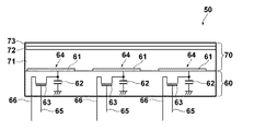
次に、本発明の放射線画像検出器の第2の実施形態について説明する。第2の実施形態の放射線画像検出器は、いわゆるTFT読取方式の放射線画像検出器である。図7は第2の実施形態の放射線画像検出器の一部断面図である。 Next, a second embodiment of the radiation image detector of the present invention will be described. The radiation image detector according to the second embodiment is a so-called TFT reading radiation image detector. FIG. 7 is a partial cross-sectional view of the radiation image detector according to the second embodiment.
第2の実施形態の放射線画像検出器50は、図7に示すように、アクティブマトリクス基板60と、このアクティブマトリクス基板60上に積層された放射線検出部70とから構成されている。
As shown in FIG. 7, the
放射線検出部70は、アクティブマトリクス基板60上の略全面に形成された半導体層71と、半導体層71上に設けられた正孔注入阻止層72と、正孔注入阻止層72上に設けられた上部電極73とを備えている。
The
半導体層71は、電磁波導電性を有するものであり、X線が照射されると膜の内部に電荷を発生するものである。半導体層71としては、たとえば、セレンを主成分とする膜厚100〜1000μmの非晶質a−Se膜を用いることができる。上記半導体層71は、アクティブマトリクス基板60上に真空蒸着法によって形成される。
The
上部電極73は、Au、Alなどの低抵抗の導電材料で形成されている。
The
アクティブマトリクス基板60は、半導体層71において発生した電荷を収集する収集電極61、収集電極61によって収集された電荷を蓄積する蓄積容量62および蓄積容量62に蓄積された電荷を読み出すためのTFTスイッチ63を有する多数の画素64とTFTスイッチ63をON/OFFするための多数の走査配線65と蓄積容量62に蓄積された電荷が読み出される多数のデータ配線66とを備えている。
The
TFTスイッチ63としては、一般的には、アモルファスシリコンを活性層に用いたa−SiTFTが用いられる。
As the
図8に、アクティブマトリクス基板60の平面図を示す。アクティブマトリクス基板60には、図8に示すように、蓄積容量62とTFTスイッチ63とを有する画素64が2次元状に多数設けられており、走査配線65とデータ配線66とが、格子状に配置されている。そして、データ配線66の終端には、データ配線66に流れ出した信号電荷を検出するアンプからなる読出回路80が接続され、走査配線65には、TFTスイッチ63をON/OFFするための制御信号を出力するゲートドライバ90が接続されている。
FIG. 8 shows a plan view of the
ここで、従来のTFT方式の放射線画像検出器においては、放射線画像の記録および読取りの際、上部電極に正の電圧が印加されるが、この正の電圧の印加により上部電極から半導体層に正孔が注入される。そうすると、図9に示すように、放射線の照射を停止した後も、上部電極から正孔が注入され、この正孔が残像電流(図9の斜線部)として検出され、読み出された画像信号にノイズが混入し、読み出された放射線画像の画質が劣化してしまう。 Here, in the conventional TFT type radiographic image detector, a positive voltage is applied to the upper electrode during recording and reading of the radiographic image. By applying this positive voltage, a positive voltage is applied from the upper electrode to the semiconductor layer. Holes are injected. Then, as shown in FIG. 9, even after the radiation irradiation is stopped, holes are injected from the upper electrode, and these holes are detected as an afterimage current (hatched portion in FIG. 9) and read out image signal. Noise is mixed in, and the image quality of the read radiation image is deteriorated.
そこで、本実施形態の放射線画像検出器50においては、上部電極73からの正孔の注入を阻止するために上部電極73と半導体層71との間に、正孔注入阻止層72を設けるようにしている。
Therefore, in the
上記第1の実施形態の放射線画像検出器と同様に、正孔注入阻止層72の正孔注入阻止の効果を十分に得るため、正孔注入阻止層72を、SbxS100−xの合金から形成し、SbxS100−xを41≦x≦60を満たすような組成比としている。なお、正孔注入阻止層72の製造方法については、上記第第1の実施形態の放射線画像検出器における正孔注入阻止層72と同様である。
Similarly to the radiation image detector of the first embodiment, in order to sufficiently obtain the hole injection blocking effect of the hole
ここで、図10に、正孔注入阻止層72のSbxS100−xの組成比を、Sb40S60とした場合における正孔注入の影響を示す。図10に示すように、最初の放射線照射時は、放射線照射時の信号電流に対する残像電流の比が桁で示すと3.5桁であったが、繰り返し放射線の照射を繰り返すと、放射線照射時の信号電流に対する残像電流の比が桁で示すと3桁まで増加し、ノイズとして無視できない量になることがわかった。
Here, FIG. 10 shows the influence of hole injection when the composition ratio of Sb x S 100-x of the hole
これに対し、正孔注入阻止層72のSbxS100−xの組成比を、Sb42S58とした場合には、最初の放射線照射時は、放射線照射時の信号電流に対する残像電流の比を桁で示すと4.5桁となり、さらにその後、放射線照射を繰り返しても正孔注入による残像電流は増加しなかった。また、正孔注入阻止層72のSbxS100−xの組成比を、Sb45S55とした場合には、正孔注入による信号電荷は、最初の放射線照射時は、最初の放射線照射時は、放射線照射時の信号電流に対する残像電流の比が桁で示すと4桁となり、さらにその後、放射線照射を繰り返しても正孔注入による残像電流は増加しなかった。
On the other hand, when the composition ratio of Sb x S 100-x of the hole
つまり、SbxS100−xを、41≦x≦60を満たすような組成比とすることによって、正孔注入による残像電流を減少させることができ、さらに放射線照射を繰り返しても正孔注入による残像電流を増加させないようにすることができる。 That is, by setting Sb x S 100-x to a composition ratio that satisfies 41 ≦ x ≦ 60, it is possible to reduce the afterimage current due to hole injection, and further, due to hole injection even if radiation irradiation is repeated. The afterimage current can be prevented from increasing.
なお、正孔注入阻止層72の厚さは0.5μmとしている。正孔注入阻止層72の厚さは、本実施形態のように0.5μmに限らず、0.25μm程度から均一な膜が得られ正孔注入阻止性能の向上を示し、また、厚くした場合には更には注入阻止性能が向上する。しかし、厚くすると製膜後にアモルファスセレン膜が得られにくくなり、結晶化部分から局所的な電荷注入が生じることから、0.25μm以上3μm以下とすることが望ましい。
The thickness of the hole
次に、上記第2の実施形態の放射線画像検出器への放射線画像の記録および読取りの作用について説明する。 Next, the operation of recording and reading a radiation image on the radiation image detector of the second embodiment will be described.
まず、図11に示すように、電圧源55によって放射線画像検出器50の上部電極に正の電圧を印加した状態において、被写体を透過して被写体の放射線画像を担持した放射線が放射線画像検出器50の上部電極73側から照射される。
First, as shown in FIG. 11, in a state where a positive voltage is applied to the upper electrode of the
そして、放射線画像検出器50に照射された放射線は、上部電極73を透過し、半導体層71に照射される。そして、その放射線の照射によって半導体層71において電荷対が発生し、そのうち負の電荷は上部電極73に帯電した正の電荷と結合して消滅し、正の電荷は潜像電荷として各画素64の各収集電極61に収集され、各蓄積容量62に蓄積されて放射線画像が記録される。
The radiation applied to the
そして、次に、図8に示すゲートドライバ90から各走査配線65にTFTスイッチ63をONするための制御信号が順次出力される。そして、各走査配線65に接続されたTFTスイッチ63がゲートドライバ90から出力された制御信号に応じてONし、各画素64の蓄積容量62からデータ配線66に蓄積電荷が読み出される。そして、データ配線66に流れ出した電荷信号は読出回路80のチャージアンプにより画像信号として検出され、放射線画像に応じた画像信号の読取りが行われる。
Next, a control signal for turning on the
本実施形態の放射線画像検出器50によれば、上部電極73と半導体層71との間に、上述した正孔注入阻止層72を設けるようにしたので、上部電極73から半導体層72への正孔注入を十分に阻止することができ、上記正孔注入による画像信号中のノイズを軽減し、読み出される放射線画像の画質の向上を図ることができる。
According to the
また、上記第2の実施形態の放射線画像検出器においては、半導体層71上に直接正孔注入阻止層72を設けるようにしたが、上記のように正孔注入阻止層72を抵抗加熱蒸着によって設けるようにした場合、上記第1の実施形態の放射線画像検出器と同様に、半導体層71に結晶核が生成し、放射線画像に欠陥を生じてしまう。
In the radiation image detector of the second embodiment, the hole
そこで、図12に示すように、正孔注入阻止層72と半導体層71との間に、SeとAsを主成分とする結晶化防止層74を設けるようにしてもよい。結晶化防止層74におけるAsの成分の割合については、上記第1の実施形態の放射線画像検出器の場合と同様に、
2%〜15%であることが望ましい。
Therefore, as shown in FIG. 12, a
It is desirable to be 2% to 15%.
また、上記実施形態においては、放射線を直接電荷に変換する、いわゆる直接変換型の放射線画像検出器について説明したが、これに限らず、放射線を蛍光体により一旦光に変換し、その光を電荷に変換する、いわゆる間接変換型の放射線画像検出器に類似する構成の放射線画像検出器にも本発明は適用することができる。なお、間接変換型の放射線画像検出器に類似する構成の放射線画像検出器とは、直接変換型の放射線画像検出器よりもa
−Se層を薄くし、光透過型の第1の電極層を設けるとともに、第1の電極層の上方に蛍光体を設け、その蛍光体からの光を電荷に変換するものである。なお、上記のように構成された放射線画像検出器においては、記録用光導電層や半導体層の厚さは1〜30μm程度となり、TFT読取方式の放射線画像検出器の場合には、蓄積容量はなくてもよい。
In the above-described embodiment, a so-called direct conversion type radiation image detector that directly converts radiation into electric charges has been described. However, the present invention is not limited thereto, and radiation is once converted into light by a phosphor and the light is charged. The present invention can also be applied to a radiation image detector having a configuration similar to a so-called indirect conversion type radiation image detector. Note that a radiation image detector having a configuration similar to the indirect conversion type radiation image detector is more than a direct conversion type radiation image detector.
The Se layer is thinned, a light transmission type first electrode layer is provided, a phosphor is provided above the first electrode layer, and light from the phosphor is converted into electric charges. In the radiation image detector configured as described above, the thickness of the recording photoconductive layer and the semiconductor layer is about 1 to 30 μm. In the case of a TFT reading type radiation image detector, the storage capacity is It does not have to be.
1 第1の電極層(電圧印加電極)
2 正孔注入阻止層
3 記録用光導電層(半導体層)
4 電荷輸送層
5 読取用光導電層
6 蓄電部
7 第2の電極層
8 透明線状電極
9 遮光線状電極
10 放射線画像検出器
11 結晶化防止層
20 高圧電源
30 チャージアンプ
50 放射線画像検出器
55 電圧源
60 アクティブマトリクス基板
61 収集電極
62 蓄積容量
63 TFTスイッチ
64 画素
65 走査配線
66 データ配線
70 放射線検出部
71 半導体層
72 正孔注入阻止層
73 上部電極(電圧印加電極)
74 結晶化防止層
80 読出回路
90 ゲートドライバ
101 第1の電極層
102 記録用光導電層
103 電荷輸送層
104 読取用光導電層
105 蓄電部
106 透明線状電極
107 遮光線状電極
1 1st electrode layer (voltage application electrode)
2 Hole
DESCRIPTION OF
74
Claims (6)
前記電圧印加電極と前記半導体層との間に、前記電圧印加電極から前記半導体層への正孔の注入を阻止する正孔注入阻止層が設けられ、
該正孔注入阻止層がSbxS100−xの合金からなり、前記xが41≦x≦60を満たすものであることを特徴とする放射線画像検出器。 A voltage application electrode to which a voltage is applied, a semiconductor layer that generates a charge when irradiated with radiation, and an electrode that detects an electrical signal corresponding to the radiation dose are stacked, and the electrode corresponds to the charge generated in the semiconductor layer. In the radiation image detector from which the image signal is read out,
Between the voltage application electrode and the semiconductor layer, a hole injection blocking layer that blocks injection of holes from the voltage application electrode to the semiconductor layer is provided,
The radiation image detector, wherein the hole injection blocking layer is made of an alloy of Sb x S 100-x , and x satisfies 41 ≦ x ≦ 60.
Priority Applications (2)
| Application Number | Priority Date | Filing Date | Title |
|---|---|---|---|
| JP2008070925A JP5207451B2 (en) | 2007-09-28 | 2008-03-19 | Radiation image detector |
| US12/240,299 US7608833B2 (en) | 2007-09-28 | 2008-09-29 | Radiation image detector |
Applications Claiming Priority (3)
| Application Number | Priority Date | Filing Date | Title |
|---|---|---|---|
| JP2007254604 | 2007-09-28 | ||
| JP2007254604 | 2007-09-28 | ||
| JP2008070925A JP5207451B2 (en) | 2007-09-28 | 2008-03-19 | Radiation image detector |
Publications (2)
| Publication Number | Publication Date |
|---|---|
| JP2009099933A JP2009099933A (en) | 2009-05-07 |
| JP5207451B2 true JP5207451B2 (en) | 2013-06-12 |
Family
ID=40702607
Family Applications (1)
| Application Number | Title | Priority Date | Filing Date |
|---|---|---|---|
| JP2008070925A Active JP5207451B2 (en) | 2007-09-28 | 2008-03-19 | Radiation image detector |
Country Status (1)
| Country | Link |
|---|---|
| JP (1) | JP5207451B2 (en) |
Family Cites Families (8)
| Publication number | Priority date | Publication date | Assignee | Title |
|---|---|---|---|---|
| JPS5534979B1 (en) * | 1969-10-27 | 1980-09-10 | ||
| JPS552699B2 (en) * | 1974-05-13 | 1980-01-22 | ||
| JPS5946738A (en) * | 1982-09-09 | 1984-03-16 | Matsushita Electronics Corp | Photoelectric conversion target and its manufacturing method |
| JPS61120586A (en) * | 1984-11-15 | 1986-06-07 | Toshiba Corp | Solid-state image pickup device |
| JPH065223A (en) * | 1992-06-19 | 1994-01-14 | Nippon Hoso Kyokai <Nhk> | Image pick-up device and its manufacture |
| JP4054168B2 (en) * | 2000-08-10 | 2008-02-27 | 日本放送協会 | Imaging device and operation method thereof |
| JP3678162B2 (en) * | 2001-04-12 | 2005-08-03 | 株式会社島津製作所 | Radiation detector |
| JP2007150278A (en) * | 2005-11-01 | 2007-06-14 | Fujifilm Corp | Radiation image taking panel and photoconductive layer forming the same |
-
2008
- 2008-03-19 JP JP2008070925A patent/JP5207451B2/en active Active
Also Published As
| Publication number | Publication date |
|---|---|
| JP2009099933A (en) | 2009-05-07 |
Similar Documents
| Publication | Publication Date | Title |
|---|---|---|
| US7786446B2 (en) | Radiation detector | |
| JP2010210590A (en) | Radiation detector | |
| US6774385B2 (en) | Image recording medium and method of manufacturing the same | |
| JP2008210906A (en) | Radiation image detector | |
| JP2009088154A (en) | Radiation detector | |
| JP4739298B2 (en) | Radiation image detector | |
| JP2007324470A (en) | Radiation image detector | |
| US7939814B2 (en) | Radiographic image detector | |
| EP1780800A2 (en) | Photoconductive layer forming radiation image taking panel and radiation image taking panel | |
| JP5235119B2 (en) | Radiation image detector | |
| JP5207451B2 (en) | Radiation image detector | |
| US7728300B2 (en) | Radiation image detector | |
| US7608833B2 (en) | Radiation image detector | |
| JP2010027834A (en) | Method for manufacturing photoconductive layer for recording of radiation detector | |
| JP4694556B2 (en) | Radiation image detector | |
| JP2004186604A (en) | Image recording medium | |
| JP2004342691A (en) | Radiation image detector | |
| JP5270121B2 (en) | Imaging device | |
| JP4787227B2 (en) | Radiation detector and method for producing photoconductive layer for recording radiation detector | |
| JP5077921B2 (en) | Radiation solid state sensor and manufacturing method thereof | |
| JP2007150277A (en) | Radiation image taking panel and photoconductive layer forming the same | |
| JP2007080927A (en) | Radiation image detector | |
| JP2010098102A (en) | Radiological image detector | |
| JP2007150278A (en) | Radiation image taking panel and photoconductive layer forming the same | |
| JP2008128725A (en) | Radiographic image reading method and radiographic image detector |
Legal Events
| Date | Code | Title | Description |
|---|---|---|---|
| A621 | Written request for application examination |
Free format text: JAPANESE INTERMEDIATE CODE: A621 Effective date: 20100707 |
|
| RD15 | Notification of revocation of power of sub attorney |
Free format text: JAPANESE INTERMEDIATE CODE: A7435 Effective date: 20110511 |
|
| A711 | Notification of change in applicant |
Free format text: JAPANESE INTERMEDIATE CODE: A711 Effective date: 20110908 |
|
| A521 | Request for written amendment filed |
Free format text: JAPANESE INTERMEDIATE CODE: A821 Effective date: 20110908 |
|
| A977 | Report on retrieval |
Free format text: JAPANESE INTERMEDIATE CODE: A971007 Effective date: 20120803 |
|
| A131 | Notification of reasons for refusal |
Free format text: JAPANESE INTERMEDIATE CODE: A131 Effective date: 20120814 |
|
| A521 | Request for written amendment filed |
Free format text: JAPANESE INTERMEDIATE CODE: A523 Effective date: 20121015 |
|
| TRDD | Decision of grant or rejection written | ||
| A01 | Written decision to grant a patent or to grant a registration (utility model) |
Free format text: JAPANESE INTERMEDIATE CODE: A01 Effective date: 20130205 |
|
| A61 | First payment of annual fees (during grant procedure) |
Free format text: JAPANESE INTERMEDIATE CODE: A61 Effective date: 20130215 |
|
| FPAY | Renewal fee payment (event date is renewal date of database) |
Free format text: PAYMENT UNTIL: 20160301 Year of fee payment: 3 |
|
| R150 | Certificate of patent or registration of utility model |
Ref document number: 5207451 Country of ref document: JP Free format text: JAPANESE INTERMEDIATE CODE: R150 Free format text: JAPANESE INTERMEDIATE CODE: R150 |
|
| R250 | Receipt of annual fees |
Free format text: JAPANESE INTERMEDIATE CODE: R250 |
|
| R250 | Receipt of annual fees |
Free format text: JAPANESE INTERMEDIATE CODE: R250 |
|
| R250 | Receipt of annual fees |
Free format text: JAPANESE INTERMEDIATE CODE: R250 |
|
| R250 | Receipt of annual fees |
Free format text: JAPANESE INTERMEDIATE CODE: R250 |
|
| R250 | Receipt of annual fees |
Free format text: JAPANESE INTERMEDIATE CODE: R250 |
|
| R250 | Receipt of annual fees |
Free format text: JAPANESE INTERMEDIATE CODE: R250 |
|
| R250 | Receipt of annual fees |
Free format text: JAPANESE INTERMEDIATE CODE: R250 |
|
| R250 | Receipt of annual fees |
Free format text: JAPANESE INTERMEDIATE CODE: R250 |
|
| R250 | Receipt of annual fees |
Free format text: JAPANESE INTERMEDIATE CODE: R250 |