JP5188256B2 - Capacitor component manufacturing method - Google Patents
Capacitor component manufacturing method Download PDFInfo
- Publication number
- JP5188256B2 JP5188256B2 JP2008118519A JP2008118519A JP5188256B2 JP 5188256 B2 JP5188256 B2 JP 5188256B2 JP 2008118519 A JP2008118519 A JP 2008118519A JP 2008118519 A JP2008118519 A JP 2008118519A JP 5188256 B2 JP5188256 B2 JP 5188256B2
- Authority
- JP
- Japan
- Prior art keywords
- capacitor
- upper electrode
- lower electrode
- capacitor component
- layer
- Prior art date
- Legal status (The legal status is an assumption and is not a legal conclusion. Google has not performed a legal analysis and makes no representation as to the accuracy of the status listed.)
- Active
Links
- 239000003990 capacitor Substances 0.000 title claims description 199
- 238000004519 manufacturing process Methods 0.000 title claims description 21
- 239000011347 resin Substances 0.000 claims description 44
- 229920005989 resin Polymers 0.000 claims description 44
- 229910052751 metal Inorganic materials 0.000 claims description 10
- 239000002184 metal Substances 0.000 claims description 10
- 239000011248 coating agent Substances 0.000 claims description 9
- 238000000576 coating method Methods 0.000 claims description 9
- 238000005530 etching Methods 0.000 claims description 7
- 238000010030 laminating Methods 0.000 claims description 5
- 238000005520 cutting process Methods 0.000 claims description 4
- 238000002788 crimping Methods 0.000 claims description 2
- 238000010438 heat treatment Methods 0.000 claims description 2
- 238000003825 pressing Methods 0.000 claims 1
- 239000010410 layer Substances 0.000 description 113
- 239000000758 substrate Substances 0.000 description 54
- RYGMFSIKBFXOCR-UHFFFAOYSA-N Copper Chemical compound [Cu] RYGMFSIKBFXOCR-UHFFFAOYSA-N 0.000 description 44
- PXHVJJICTQNCMI-UHFFFAOYSA-N Nickel Chemical compound [Ni] PXHVJJICTQNCMI-UHFFFAOYSA-N 0.000 description 44
- 229910052802 copper Inorganic materials 0.000 description 29
- 239000010949 copper Substances 0.000 description 29
- 239000004065 semiconductor Substances 0.000 description 29
- 238000000034 method Methods 0.000 description 25
- 238000007747 plating Methods 0.000 description 24
- 229910052759 nickel Inorganic materials 0.000 description 22
- 239000011889 copper foil Substances 0.000 description 15
- 239000011229 interlayer Substances 0.000 description 13
- 229910000679 solder Inorganic materials 0.000 description 11
- 238000000059 patterning Methods 0.000 description 6
- 239000000463 material Substances 0.000 description 4
- 238000005245 sintering Methods 0.000 description 4
- 229910052454 barium strontium titanate Inorganic materials 0.000 description 2
- 238000005304 joining Methods 0.000 description 2
- 229910052451 lead zirconate titanate Inorganic materials 0.000 description 2
- HFGPZNIAWCZYJU-UHFFFAOYSA-N lead zirconate titanate Chemical compound [O-2].[O-2].[O-2].[O-2].[O-2].[Ti+4].[Zr+4].[Pb+2] HFGPZNIAWCZYJU-UHFFFAOYSA-N 0.000 description 2
- RTAQQCXQSZGOHL-UHFFFAOYSA-N Titanium Chemical compound [Ti] RTAQQCXQSZGOHL-UHFFFAOYSA-N 0.000 description 1
- 229910002113 barium titanate Inorganic materials 0.000 description 1
- JRPBQTZRNDNNOP-UHFFFAOYSA-N barium titanate Chemical compound [Ba+2].[Ba+2].[O-][Ti]([O-])([O-])[O-] JRPBQTZRNDNNOP-UHFFFAOYSA-N 0.000 description 1
- 230000015572 biosynthetic process Effects 0.000 description 1
- 229910002115 bismuth titanate Inorganic materials 0.000 description 1
- 239000000919 ceramic Substances 0.000 description 1
- RYGMFSIKBFXOCR-YPZZEJLDSA-N copper-62 Chemical compound [62Cu] RYGMFSIKBFXOCR-YPZZEJLDSA-N 0.000 description 1
- 238000009792 diffusion process Methods 0.000 description 1
- 238000005553 drilling Methods 0.000 description 1
- 230000000694 effects Effects 0.000 description 1
- PCHJSUWPFVWCPO-UHFFFAOYSA-N gold Chemical compound [Au] PCHJSUWPFVWCPO-UHFFFAOYSA-N 0.000 description 1
- 229910052737 gold Inorganic materials 0.000 description 1
- 239000010931 gold Substances 0.000 description 1
- 229910052746 lanthanum Inorganic materials 0.000 description 1
- FZLIPJUXYLNCLC-UHFFFAOYSA-N lanthanum atom Chemical compound [La] FZLIPJUXYLNCLC-UHFFFAOYSA-N 0.000 description 1
- 239000012299 nitrogen atmosphere Substances 0.000 description 1
- 230000001681 protective effect Effects 0.000 description 1
- 238000007789 sealing Methods 0.000 description 1
- 239000007787 solid Substances 0.000 description 1
- 238000004544 sputter deposition Methods 0.000 description 1
- 230000006641 stabilisation Effects 0.000 description 1
- 238000011105 stabilization Methods 0.000 description 1
- VEALVRVVWBQVSL-UHFFFAOYSA-N strontium titanate Chemical compound [Sr+2].[O-][Ti]([O-])=O VEALVRVVWBQVSL-UHFFFAOYSA-N 0.000 description 1
- 238000007740 vapor deposition Methods 0.000 description 1
Images


Classifications
-
- H—ELECTRICITY
- H05—ELECTRIC TECHNIQUES NOT OTHERWISE PROVIDED FOR
- H05K—PRINTED CIRCUITS; CASINGS OR CONSTRUCTIONAL DETAILS OF ELECTRIC APPARATUS; MANUFACTURE OF ASSEMBLAGES OF ELECTRICAL COMPONENTS
- H05K1/00—Printed circuits
- H05K1/16—Printed circuits incorporating printed electric components, e.g. printed resistor, capacitor, inductor
- H05K1/162—Printed circuits incorporating printed electric components, e.g. printed resistor, capacitor, inductor incorporating printed capacitors
-
- H—ELECTRICITY
- H01—ELECTRIC ELEMENTS
- H01G—CAPACITORS; CAPACITORS, RECTIFIERS, DETECTORS, SWITCHING DEVICES OR LIGHT-SENSITIVE DEVICES, OF THE ELECTROLYTIC TYPE
- H01G4/00—Fixed capacitors; Processes of their manufacture
- H01G4/002—Details
- H01G4/228—Terminals
- H01G4/232—Terminals electrically connecting two or more layers of a stacked or rolled capacitor
-
- H—ELECTRICITY
- H01—ELECTRIC ELEMENTS
- H01G—CAPACITORS; CAPACITORS, RECTIFIERS, DETECTORS, SWITCHING DEVICES OR LIGHT-SENSITIVE DEVICES, OF THE ELECTROLYTIC TYPE
- H01G4/00—Fixed capacitors; Processes of their manufacture
- H01G4/002—Details
- H01G4/228—Terminals
- H01G4/236—Terminals leading through the housing, i.e. lead-through
-
- H—ELECTRICITY
- H01—ELECTRIC ELEMENTS
- H01G—CAPACITORS; CAPACITORS, RECTIFIERS, DETECTORS, SWITCHING DEVICES OR LIGHT-SENSITIVE DEVICES, OF THE ELECTROLYTIC TYPE
- H01G4/00—Fixed capacitors; Processes of their manufacture
- H01G4/33—Thin- or thick-film capacitors
-
- H—ELECTRICITY
- H01—ELECTRIC ELEMENTS
- H01L—SEMICONDUCTOR DEVICES NOT COVERED BY CLASS H10
- H01L23/00—Details of semiconductor or other solid state devices
- H01L23/48—Arrangements for conducting electric current to or from the solid state body in operation, e.g. leads, terminal arrangements ; Selection of materials therefor
- H01L23/488—Arrangements for conducting electric current to or from the solid state body in operation, e.g. leads, terminal arrangements ; Selection of materials therefor consisting of soldered or bonded constructions
- H01L23/498—Leads, i.e. metallisations or lead-frames on insulating substrates, e.g. chip carriers
- H01L23/49822—Multilayer substrates
-
- H—ELECTRICITY
- H01—ELECTRIC ELEMENTS
- H01L—SEMICONDUCTOR DEVICES NOT COVERED BY CLASS H10
- H01L23/00—Details of semiconductor or other solid state devices
- H01L23/48—Arrangements for conducting electric current to or from the solid state body in operation, e.g. leads, terminal arrangements ; Selection of materials therefor
- H01L23/50—Arrangements for conducting electric current to or from the solid state body in operation, e.g. leads, terminal arrangements ; Selection of materials therefor for integrated circuit devices, e.g. power bus, number of leads
-
- H—ELECTRICITY
- H01—ELECTRIC ELEMENTS
- H01L—SEMICONDUCTOR DEVICES NOT COVERED BY CLASS H10
- H01L28/00—Passive two-terminal components without a potential-jump or surface barrier for integrated circuits; Details thereof; Multistep manufacturing processes therefor
- H01L28/40—Capacitors
-
- H—ELECTRICITY
- H01—ELECTRIC ELEMENTS
- H01L—SEMICONDUCTOR DEVICES NOT COVERED BY CLASS H10
- H01L2224/00—Indexing scheme for arrangements for connecting or disconnecting semiconductor or solid-state bodies and methods related thereto as covered by H01L24/00
- H01L2224/01—Means for bonding being attached to, or being formed on, the surface to be connected, e.g. chip-to-package, die-attach, "first-level" interconnects; Manufacturing methods related thereto
- H01L2224/10—Bump connectors; Manufacturing methods related thereto
- H01L2224/15—Structure, shape, material or disposition of the bump connectors after the connecting process
- H01L2224/16—Structure, shape, material or disposition of the bump connectors after the connecting process of an individual bump connector
- H01L2224/161—Disposition
- H01L2224/16151—Disposition the bump connector connecting between a semiconductor or solid-state body and an item not being a semiconductor or solid-state body, e.g. chip-to-substrate, chip-to-passive
- H01L2224/16221—Disposition the bump connector connecting between a semiconductor or solid-state body and an item not being a semiconductor or solid-state body, e.g. chip-to-substrate, chip-to-passive the body and the item being stacked
- H01L2224/16225—Disposition the bump connector connecting between a semiconductor or solid-state body and an item not being a semiconductor or solid-state body, e.g. chip-to-substrate, chip-to-passive the body and the item being stacked the item being non-metallic, e.g. insulating substrate with or without metallisation
-
- H—ELECTRICITY
- H01—ELECTRIC ELEMENTS
- H01L—SEMICONDUCTOR DEVICES NOT COVERED BY CLASS H10
- H01L25/00—Assemblies consisting of a plurality of individual semiconductor or other solid state devices ; Multistep manufacturing processes thereof
- H01L25/03—Assemblies consisting of a plurality of individual semiconductor or other solid state devices ; Multistep manufacturing processes thereof all the devices being of a type provided for in the same subgroup of groups H01L27/00 - H01L33/00, or in a single subclass of H10K, H10N, e.g. assemblies of rectifier diodes
- H01L25/04—Assemblies consisting of a plurality of individual semiconductor or other solid state devices ; Multistep manufacturing processes thereof all the devices being of a type provided for in the same subgroup of groups H01L27/00 - H01L33/00, or in a single subclass of H10K, H10N, e.g. assemblies of rectifier diodes the devices not having separate containers
- H01L25/065—Assemblies consisting of a plurality of individual semiconductor or other solid state devices ; Multistep manufacturing processes thereof all the devices being of a type provided for in the same subgroup of groups H01L27/00 - H01L33/00, or in a single subclass of H10K, H10N, e.g. assemblies of rectifier diodes the devices not having separate containers the devices being of a type provided for in group H01L27/00
- H01L25/0652—Assemblies consisting of a plurality of individual semiconductor or other solid state devices ; Multistep manufacturing processes thereof all the devices being of a type provided for in the same subgroup of groups H01L27/00 - H01L33/00, or in a single subclass of H10K, H10N, e.g. assemblies of rectifier diodes the devices not having separate containers the devices being of a type provided for in group H01L27/00 the devices being arranged next and on each other, i.e. mixed assemblies
-
- H—ELECTRICITY
- H01—ELECTRIC ELEMENTS
- H01L—SEMICONDUCTOR DEVICES NOT COVERED BY CLASS H10
- H01L2924/00—Indexing scheme for arrangements or methods for connecting or disconnecting semiconductor or solid-state bodies as covered by H01L24/00
- H01L2924/15—Details of package parts other than the semiconductor or other solid state devices to be connected
- H01L2924/151—Die mounting substrate
- H01L2924/153—Connection portion
- H01L2924/1531—Connection portion the connection portion being formed only on the surface of the substrate opposite to the die mounting surface
- H01L2924/15311—Connection portion the connection portion being formed only on the surface of the substrate opposite to the die mounting surface being a ball array, e.g. BGA
-
- H—ELECTRICITY
- H01—ELECTRIC ELEMENTS
- H01L—SEMICONDUCTOR DEVICES NOT COVERED BY CLASS H10
- H01L2924/00—Indexing scheme for arrangements or methods for connecting or disconnecting semiconductor or solid-state bodies as covered by H01L24/00
- H01L2924/15—Details of package parts other than the semiconductor or other solid state devices to be connected
- H01L2924/151—Die mounting substrate
- H01L2924/153—Connection portion
- H01L2924/1532—Connection portion the connection portion being formed on the die mounting surface of the substrate
- H01L2924/1533—Connection portion the connection portion being formed on the die mounting surface of the substrate the connection portion being formed both on the die mounting surface of the substrate and outside the die mounting surface of the substrate
- H01L2924/15331—Connection portion the connection portion being formed on the die mounting surface of the substrate the connection portion being formed both on the die mounting surface of the substrate and outside the die mounting surface of the substrate being a ball array, e.g. BGA
-
- H—ELECTRICITY
- H05—ELECTRIC TECHNIQUES NOT OTHERWISE PROVIDED FOR
- H05K—PRINTED CIRCUITS; CASINGS OR CONSTRUCTIONAL DETAILS OF ELECTRIC APPARATUS; MANUFACTURE OF ASSEMBLAGES OF ELECTRICAL COMPONENTS
- H05K2201/00—Indexing scheme relating to printed circuits covered by H05K1/00
- H05K2201/09—Shape and layout
- H05K2201/09209—Shape and layout details of conductors
- H05K2201/095—Conductive through-holes or vias
- H05K2201/09509—Blind vias, i.e. vias having one side closed
- H05K2201/09518—Deep blind vias, i.e. blind vias connecting the surface circuit to circuit layers deeper than the first buried circuit layer
-
- H—ELECTRICITY
- H05—ELECTRIC TECHNIQUES NOT OTHERWISE PROVIDED FOR
- H05K—PRINTED CIRCUITS; CASINGS OR CONSTRUCTIONAL DETAILS OF ELECTRIC APPARATUS; MANUFACTURE OF ASSEMBLAGES OF ELECTRICAL COMPONENTS
- H05K2201/00—Indexing scheme relating to printed circuits covered by H05K1/00
- H05K2201/09—Shape and layout
- H05K2201/09209—Shape and layout details of conductors
- H05K2201/09654—Shape and layout details of conductors covering at least two types of conductors provided for in H05K2201/09218 - H05K2201/095
- H05K2201/09718—Clearance holes
-
- H—ELECTRICITY
- H05—ELECTRIC TECHNIQUES NOT OTHERWISE PROVIDED FOR
- H05K—PRINTED CIRCUITS; CASINGS OR CONSTRUCTIONAL DETAILS OF ELECTRIC APPARATUS; MANUFACTURE OF ASSEMBLAGES OF ELECTRICAL COMPONENTS
- H05K2201/00—Indexing scheme relating to printed circuits covered by H05K1/00
- H05K2201/09—Shape and layout
- H05K2201/09209—Shape and layout details of conductors
- H05K2201/09654—Shape and layout details of conductors covering at least two types of conductors provided for in H05K2201/09218 - H05K2201/095
- H05K2201/09763—Printed component having superposed conductors, but integrated in one circuit layer
Description
本発明はキャパシタ部品およびその製造方法ならびに半導体パッケージに関し、より詳細には半導体パッケージ等に内蔵して用いることができるキャパシタ部品およびその製造方法、ならびにキャパシタ部品を用いた半導体パッケージに関する。 The present invention relates to a capacitor component, a method for manufacturing the same, and a semiconductor package. More specifically, the present invention relates to a capacitor component that can be used in a semiconductor package or the like, a method for manufacturing the same, and a semiconductor package using the capacitor component.
半導体パッケージの特性を改善することを目的として、デカップリングキャパシタを配線基板に内蔵する方法が従来、検討されてきた。デカップリングキャパシタを内蔵した配線基板は、基板上にチップコンデンサ等の部品を配置する方法とくらべて、半導体チップとの配線距離を短縮して半導体装置の特性を改善することができ、また効果的に電子部品を小型化できるという利点がある。 In order to improve the characteristics of a semiconductor package, a method of incorporating a decoupling capacitor in a wiring board has been conventionally studied. A wiring board with a built-in decoupling capacitor can shorten the wiring distance to the semiconductor chip and improve the characteristics of the semiconductor device, and is more effective than the method of placing components such as chip capacitors on the board. There is an advantage that electronic parts can be miniaturized.
デカップリングキャパシタを配線基板に設ける方法としては、基板表面に誘電体膜を印刷してデカップリングキャパシタとする方法、Si板の表面に誘電体膜を形成したデカップリングキャパシタを基板に内蔵する方法、セラミックチップコンデンサあるいは固体電解コンデンサを基板に内蔵させる方法等がある。また、誘電体層を金属層で挟んだシート材を使用して基板にキャパシタを内蔵する方法もある(特許文献1)。
基板に内蔵するデカップリングキャパシタとしてはある程度の電気容量を有することが求められる。誘電体膜を印刷してデカップリングキャパシタとする方法は、高容量化が困難であり、1μF/cm2程度の電気容量を得ることが難しい。
また、Si基板の表面に誘電体膜を形成してキャパシタとする方法の場合は、Si基板の表面に誘電体を塗布した後、高温で焼結させるため、焼結時に誘電体がSi中に拡散しないように、誘電体層の下地層を設ける必要があり、下地層としてPt等の耐熱性の金属を使用することによって、製造コストがかかるという問題がある。
また、基板内にチップコンデンサを埋設する方法の場合は、チップコンデンサの厚さによって基板の全厚が厚くなるという問題がある。また、基板の厚さを抑えるために、小型のチップコンデンサを使用した場合は、大きな電気容量が得られなくなるという問題がある。
The decoupling capacitor built in the substrate is required to have a certain amount of electric capacity. In the method of printing a dielectric film to form a decoupling capacitor, it is difficult to increase the capacity, and it is difficult to obtain an electric capacity of about 1 μF / cm 2 .
In addition, in the case of a method of forming a capacitor by forming a dielectric film on the surface of the Si substrate, the dielectric is applied to the surface of the Si substrate and then sintered at a high temperature. In order to prevent diffusion, it is necessary to provide a base layer of a dielectric layer, and using a heat-resistant metal such as Pt as the base layer has a problem that manufacturing costs are increased.
In addition, in the method of embedding a chip capacitor in the substrate, there is a problem that the total thickness of the substrate is increased depending on the thickness of the chip capacitor. In addition, when a small chip capacitor is used to suppress the thickness of the substrate, there is a problem that a large electric capacity cannot be obtained.
本発明は、これらの課題を解決すべくなされたものであり、薄型化が可能で配線基板に内蔵した場合であっても基板の全厚を抑えることができ、また大きな電気容量を得ることができて配線基板に内蔵するキャパシタとして好適に使用することができるキャパシタ部品を提供するとともに、キャパシタ部品の製造方法ならびにキャパシタ部品を用いた半導体パッケージを提供することを目的とする。 The present invention has been made to solve these problems, and can be reduced in thickness, and even when incorporated in a wiring board, the total thickness of the board can be suppressed, and a large electric capacity can be obtained. An object of the present invention is to provide a capacitor component that can be suitably used as a capacitor built in a wiring board, and to provide a method for manufacturing the capacitor component and a semiconductor package using the capacitor component.
上記目的を達成するために、本発明は次の構成を備える。
すなわち、本発明に係るキャパシタ部品は、平板状に形成された上部電極および下部電極と、前記上部電極と下部電極とによって挟まれて配置された誘電体層と、前記上部電極および下部電極の外面を被覆する絶縁樹脂からなる被覆部とを備え、前記被覆部の外面が、粗面であることを特徴とする。
In order to achieve the above object, the present invention comprises the following arrangement.
That is, the capacitor component according to the present invention includes an upper electrode and a lower electrode formed in a flat plate shape, a dielectric layer disposed between the upper electrode and the lower electrode, and outer surfaces of the upper electrode and the lower electrode. and a covering portion made of an insulating resin for covering the outer surface of the cover portion, wherein the rough surface der Rukoto.
前記上部電極と下部電極の少なくとも一方に、基板にキャパシタ部品を内蔵する際に、配線パターンに接続して形成されるビアよりも大径に形成された開口穴が、少なくとも一つ設けられていることにより、開口穴位置に接続用のビア穴を形成することにより、キャパシタ部品の一方の面側から上部電極と下部電極にビアを接続することができる。
また、前記上部電極と下部電極の双方に、前記ビアよりも大径に形成された開口穴と、前記ビアよりも小径に形成された開口穴が設けられ、前記上部電極と下部電極に形成された小径の開口穴が、前記下部電極と上部電極にそれぞれ形成された大径の開口穴の平面領域内に位置するように設けられていることにより、小径の開口穴位置に合わせてビアを形成することによって、キャパシタ部品を貫通するようにビアを形成して、一方のビアを上部電極に他方のビアを下部電極に接続することができる。
At least one of the upper electrode and the lower electrode is provided with at least one opening hole having a diameter larger than a via formed in connection with a wiring pattern when a capacitor component is built in the substrate. Accordingly, by forming a via hole for connection at the position of the opening hole, the via can be connected to the upper electrode and the lower electrode from one surface side of the capacitor component.
Further, both the upper electrode and the lower electrode are provided with an opening hole having a diameter larger than that of the via and an opening hole having a diameter smaller than that of the via, and are formed in the upper electrode and the lower electrode. A small-diameter opening hole is provided so as to be located in the plane area of the large-diameter opening hole formed in each of the lower electrode and the upper electrode, thereby forming a via in accordance with the position of the small-diameter opening hole. By doing so, vias can be formed so as to penetrate the capacitor component, and one via can be connected to the upper electrode and the other via can be connected to the lower electrode.
また、金属からなる支持層の表面に誘電体層が積層され、誘電体層に金属層が積層されて形成されたキャパシタシートを使用するキャパシタ部品の製造方法であって、前記金属層と前記支持層を所定パターンにエッチングし、それぞれ上部電極と下部電極として形成する工程と、絶縁樹脂が被着した板を用い、前記絶縁樹脂が被着した面を前記キャパシタシートに向け、前記板を加熱および加圧して、前記上部電極と下部電極が形成された前記キャパシタシートの両面に前記絶縁樹脂を圧着した後、前記板を除去して、前記キャパシタシートの面を前記絶縁樹脂により被覆する工程と、前記絶縁樹脂による被覆部が形成された前記キャパシタシートを個片のキャパシタ部品に切断する工程とを備え、前記板は、前記絶縁樹脂が被着する面が粗面に形成され、前記板を除去することにより、前記絶縁樹脂による前記被覆部の外面が粗面に形成されることを特徴とする。 The dielectric layer on the surface of a support layer made of a metal are stacked, a capacitor component manufacturing method that uses a capacitor sheet having a metal layer is formed by laminating a dielectric layer, the support and the metal layer Etching the layer into a predetermined pattern, respectively, forming a top electrode and a bottom electrode , using a plate coated with an insulating resin, with the surface coated with the insulating resin facing the capacitor sheet, heating the plate and pressurizing, after crimping the insulating resin on both surfaces of the capacitor sheet which the upper and lower electrodes are formed, a step of removing the plate, coating the surface of the capacitor sheet by the insulating resin, and a step of cutting the capacitor sheet, the coating of which is formed by the insulating resin in the capacitor parts pieces, the plate, the surface of the insulating resin is deposited crude To be formed, by removing the plate, and wherein the Rukoto formed on the outer surface is rough surface of the coating portion by the insulating resin.
また、本発明に係る配線基板は、平板状に形成された上部電極および下部電極と、前記上部電極と下部電極とによって挟まれて配置された誘電体層と、前記上部電極および下部電極の外面を被覆する絶縁樹脂からなる被覆部とを備えるキャパシタ部品を有しており、前記キャパシタ部品の被覆部の外面が粗面に形成されており、前記キャパシタ部品が層間絶縁層に埋設されて、前記被覆部の外面と前記層間絶縁層が密着しており、ビアを介して前記上部電極および下部電極と配線パターンとが電気的に接続されていることを特徴とする。
また、配線基板の構成として、前記キャパシタ部品は、前記上部電極と下部電極の双方に、前記ビアよりも大径に形成された開口穴と、前記ビアよりも小径に形成された開口穴が設けられるとともに、前記上部電極と下部電極に形成された小径の開口穴が、前記下部電極と上部電極にそれぞれ形成された大径の開口穴の平面領域内に位置するように設けられ、前記ビアは、前記上部電極と下部電極にそれぞれ形成された小径の開口穴に位置合わせして、前記層間絶縁層と前記キャパシタ部品を厚さ方向に貫通して設けられ、前記ビアの一方は、前記上部電極と電気的に接続され、他方は、前記下部電極と電気的に接続されていることを特徴とする。
また、配線基板の構成として、前記キャパシタ部品は、前記上部電極と下部電極の少なくとも一方に、前記ビアよりも大径に形成された開口穴が、少なくとも一つ設けられ、前記ビアの一方は、前記上部電極と下部電極の一方に接続され、他方は、前記開口穴位置に位置合わせして前記上部電極と下部電極の他方に接続されていることを特徴とする。
The wiring board according to the present invention includes an upper electrode and a lower electrode formed in a flat plate shape, a dielectric layer disposed between the upper electrode and the lower electrode, and outer surfaces of the upper electrode and the lower electrode. A capacitor part including a covering part made of an insulating resin covering the capacitor part, the outer surface of the covering part of the capacitor part is formed in a rough surface, and the capacitor part is embedded in an interlayer insulating layer, The outer surface of the covering portion and the interlayer insulating layer are in close contact, and the upper electrode, the lower electrode, and the wiring pattern are electrically connected via vias.
Further, as a configuration of the wiring board, the capacitor component is provided with an opening hole having a diameter larger than that of the via and an opening hole having a diameter smaller than that of the via in both the upper electrode and the lower electrode. In addition, a small-diameter opening hole formed in the upper electrode and the lower electrode is provided so as to be located in a plane region of a large-diameter opening hole formed in each of the lower electrode and the upper electrode, and the via is The interlayer insulating layer and the capacitor component are provided in the thickness direction so as to be aligned with the small-diameter opening holes formed in the upper electrode and the lower electrode, respectively, and one of the vias is provided on the upper electrode. And the other is electrically connected to the lower electrode.
In addition, as a configuration of the wiring board, the capacitor component is provided with at least one opening hole having a diameter larger than that of the via in at least one of the upper electrode and the lower electrode, One of the upper electrode and the lower electrode is connected, and the other is connected to the other of the upper electrode and the lower electrode in alignment with the position of the opening hole.
また、本発明に係る配線基板は、平板状に形成された上部電極および下部電極と、前記上部電極と下部電極とによって挟まれて配置された誘電体層と、前記上部電極および下部電極の外面を被覆する絶縁樹脂からなる被覆部とを備えるキャパシタ構造をコア基板に備え、前記被覆部の外面が、粗面であり、前記被覆部の粗面上に形成された配線パターンと、前記上部電極および下部電極とが、ビアを介して電気的に接続され、前記ビアの外周が、前記誘電体層と接し、前記配線パターンを被覆するソルダーレジストが形成されていることを特徴とする。
また、配線基板の他の構成として、前記キャパシタ構造は、前記上部電極と下部電極の双方に、前記ビアよりも大径に形成された開口穴と、前記ビアよりも小径に形成された開口穴が設けられるとともに、前記上部電極と下部電極に形成された小径の開口穴が、前記下部電極と上部電極にそれぞれ形成された大径の開口穴の平面領域内に位置するように設けられ、前記ビアは、前記上部電極と下部電極にそれぞれ形成された小径の開口穴に位置合わせして、前記コア基板を厚さ方向に貫通して設けられ、前記ビアの一方は、前記上部電極と電気的に接続され、他方は、前記下部電極と電気的に接続されていることを特徴とする。
また、配線基板の他の構成として、前記キャパシタ構造は、前記上部電極と下部電極の少なくとも一方に、前記ビアよりも大径に形成された開口穴が、少なくとも一つ設けられ、前記ビアの一方は、前記上部電極と下部電極の一方に接続され、他方は、前記開口穴位置に位置合わせして前記上部電極と下部電極の他方に接続されていることを特徴とする。
The wiring board according to the present invention includes an upper electrode and a lower electrode formed in a flat plate shape, a dielectric layer disposed between the upper electrode and the lower electrode, and outer surfaces of the upper electrode and the lower electrode. A core substrate having a capacitor structure including a covering portion made of an insulating resin for covering the wiring portion, an outer surface of the covering portion being a rough surface, a wiring pattern formed on the rough surface of the covering portion, and the upper electrode And a lower electrode is electrically connected through a via, and an outer periphery of the via is in contact with the dielectric layer, and a solder resist that covers the wiring pattern is formed .
As another configuration of the wiring board, the capacitor structure includes an opening hole formed in a larger diameter than the via and an opening hole formed in a smaller diameter than the via in both the upper electrode and the lower electrode. Are provided so that the small-diameter opening holes formed in the upper electrode and the lower electrode are located in the plane area of the large-diameter opening holes formed in the lower electrode and the upper electrode, respectively. Vias are provided through the core substrate in the thickness direction in alignment with small-diameter opening holes formed in the upper electrode and the lower electrode, respectively, and one of the vias is electrically connected to the upper electrode. And the other is electrically connected to the lower electrode.
As another configuration of the wiring board, in the capacitor structure, at least one opening hole having a diameter larger than that of the via is provided in at least one of the upper electrode and the lower electrode. Is connected to one of the upper electrode and the lower electrode, and the other is connected to the other of the upper electrode and the lower electrode in alignment with the position of the opening hole.
本発明に係るキャパシタ部品は、誘電体層を上部電極と下部電極とによって挟む構造とし、被覆部によって外面を被覆したことによって、薄型、小型化を図ることができ、また所要の電気容量を確保することができて、基板に内蔵するキャパシタ部品として好適に用いられる。また、本発明に係る半導体パッケージはキャパシタ部品を内蔵した配線基板として提供され、基板の小型化が図られるとともに、電源の安定化等の機能を備えた製品として提供される。また、コア基板にキャパシタ構造を備えた半導体パッケージは、デカップリングキャパシタを備えた基板としてさらに小型化、薄型化を図ることができる。 The capacitor component according to the present invention has a structure in which the dielectric layer is sandwiched between the upper electrode and the lower electrode, and the outer surface is covered with the covering portion, so that the thin and small size can be achieved, and the required electric capacity is ensured. Therefore, it is preferably used as a capacitor component built in the substrate. In addition, the semiconductor package according to the present invention is provided as a wiring board with a built-in capacitor component, and is provided as a product having functions such as stabilization of a power source as well as miniaturization of the board. In addition, a semiconductor package having a capacitor structure on a core substrate can be further reduced in size and thickness as a substrate having a decoupling capacitor.
(キャパシタ部品)
まず、本発明に係るキャパシタ部品の製造方法について説明する。
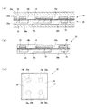
図1(a)は、キャパシタ部品の製造に用いるキャパシタシート10を示す。このキャパシタシート10は、キャパシタシート10の支持層としてのニッケル層12と、誘電体層14と銅箔16とを積層した構造に形成されている。
キャパシタシート10はあらかじめ大判の板体状に形成された製品であり、本発明に係るキャパシタ部品はこのキャパシタシート10を利用して製造する。
(Capacitor parts)
First, a method for manufacturing a capacitor component according to the present invention will be described.
Fig.1 (a) shows the
The
誘電体層14は、支持層であるニッケル層12の表面に焼結して形成されている。ニッケル層12はキャパシタシート10を保形できる厚さに形成するが、同時に誘電体を焼結させて誘電体層14を形成する支持体としても機能する。誘電体の焼結温度は高温であるが、ニッケルは窒素雰囲気中においては十分に耐熱性があり、ニッケル層12を支持体として誘電体を焼結することによってニッケル層12の表面に誘電体層14を形成することができる。
The
本実施形態においては、誘電体層14として、BST(Barium Strontium Titanate)を厚さ500nmに形成したものを使用した。誘電体層14には、この他に、チタン酸バリウム、チタン酸ストロンチウム、PZT(Lead Zirconate Titanate)、PLZT(Lead Lanthanum Zirconate Titanate)、チタン酸ビスマス等の高誘電率材料を使用することができる。
また、ニッケル層12は厚さ35μmのものを使用した。銅箔16は誘電体層14の上に蒸着法またはスパッタ法により形成したものである。
In the present embodiment, a
The
図1(b)は、キャパシタ部品の上部電極を形成するため、銅箔16をめっき給電層とする電解銅めっきにより、銅箔16の表面に銅めっき層16aを厚付けした状態を示す。銅箔16の厚さは2μm程度であり、銅めっきにより18μm程度の厚さに銅めっき層16aを形成する。
なお、キャパシタシート10の表面に形成した銅箔(金属層)が所要の厚さに形成されている場合には、銅めっき等によって金属層を厚付けする必要はない。
FIG. 1B shows a state in which the
In addition, when the copper foil (metal layer) formed in the surface of the
図1(c)、(d)は、銅めっき層16aと銅箔16をパターニングしてキャパシタ部品の上部電極18を形成する工程を示す。
図1(c)は、上部電極18の平面パターンにしたがってレジストパターン19を形成した状態を示す。銅めっき層16aの表面にドライフィルムレジストをラミネートし、露光及び現像によりレジストパターン19を形成する。次いで、レジストパターン19をマスクとして銅めっき層16aと銅箔16をエッチングし、底面に誘電体層14が露出する開口穴18a、18bを形成する。
1C and 1D show a process of patterning the
FIG. 1C shows a state in which a
図1(d)は、開口穴18a、18bを形成した後、レジストパターン19を除去した状態を示す。銅めっき層16aと銅箔16は同一の銅材からなるから、銅のエッチング液により同時にエッチングされてパターン化される。このエッチング工程においては、必要に応じて、ニッケル層12をドライフィルムによって被覆し、エッチング液からニッケル層12を保護する。
FIG. 1D shows a state in which the resist
図3に、キャパシタ部品に形成する上部電極の平面パターン例を示す。この例では、小径の平面形状が円形の開口穴18aと大径の平面形状が円形の開口穴18bを交差配置にそれぞれ2個ずつ設けている。小径の開口穴18aはキャパシタ部品を基板に内蔵する際に、ビアを介して上部電極と配線パターンとを層間で電気的に接続するためのものである。大径の開口穴18bは、配線パターンとキャパシタ部品の下部電極とを接続させるためのものであり、配線パターンと下部電極とをビアによって接続する際に、ビアが上部電極18と干渉しないようにビアが余裕をもって通過できる径に形成する。上部電極18に設ける開口穴18a、18bの配置、配置数は任意に設定することができる。
FIG. 3 shows an example of a planar pattern of the upper electrode formed on the capacitor component. In this example, two opening
上部電極18の外形形状は、上部電極18の外形位置に沿って設けられるスリット溝18cによって規定される。図3の上部電極18は平面形状が正方形に形成されているが、上部電極の平面形状は任意に設定することができる。キャパシタ部品では下部電極も上部電極と合わせた平面形状に形成される。上部電極と下部電極とで挟まれた誘電体層14の平面積が電気容量に関係し、上部電極と下部電極の平面積を広くとることによってキャパシタ部品の電気容量を大きくすることができる。
The outer shape of the
図1(e)、(f)は、ニッケル層12をパターニングしてキャパシタ部品の下部電極20を形成する工程を示す。
図1(e)は、ニッケル層12をエッチングした状態を示す。本実施形態では、エッチングにより、厚さ35μmのニッケル層12を20μmの厚さにまで薄くした。ニッケル層12をエッチングする際に、必要に応じ、上部電極18をドライフィルムレジストによって被覆して上部電極18を保護する。ニッケル層12をエッチングするのは、キャパシタ部品の厚さをできるだけ薄くするためである。
1E and 1F show a process of patterning the
FIG. 1E shows a state where the
図1(f)はエッチングしたニッケル層12をパターニングして下部電極20を形成した状態を示す。下部電極20も上部電極18を形成する場合と同様に、ニッケル層12の表面にドライフィルムレジストをラミネートし、露光及び現像してレジストパターンを形成した後、レジストパターンをマスクとしてニッケル層12をエッチングして形成する。ニッケル層12を選択的にエッチングするエッチング液を使用することによって、銅からなる上部電極18には損傷を与えずにエッチングすることができる。
FIG. 1F shows a state where the etched
図3(b)に下部電極20の平面パターン例を示す。この下部電極20の平面パターンは、図3(a)に示す上部電極18と対として用いるもので、上部電極18に形成した小径の開口穴18aの位置には下部電極20の大径の開口穴20bが位置し、上部電極18の大径の開口穴18bの位置には下部電極20の小径の開口穴20aがそれぞれ平面形状が円形に形成され、同芯配置に設けられている。下部電極20の外形位置はスリット溝20cによって規定される。上部電極18と下部電極20の平面形状は同一である。
なお、上部電極18と下部電極20に設ける開口穴は、必ずしも円形でなければならないものではない。
FIG. 3B shows an example of a planar pattern of the
The opening holes provided in the
前述したように、キャパシタシート10は大判のシート体として提供される。図1は、キャパシタシート10に形成する単位のキャパシタ部品の領域を示す。キャパシタシート10のニッケル層12や銅箔16、銅めっき層16aをパターニングして上部電極18および下部電極20を形成する際には、キャパシタシート10のすべての単位領域に図1、図2に示したパターンと同一のパターンに上部電極18と下部電極20を形成する。もちろん、各単位領域ごとに別のパターンに上部電極18と下部電極20を形成することも可能である。ニッケル層12と銅箔16、銅めっき層16aをパターニングするレジストパターンは任意にパターン形成できるからである。
As described above, the
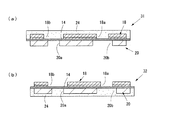
キャパシタシート10の両面に上部電極18と下部電極20を形成した後、キャパシタシート10の両面を絶縁樹脂によって被覆する工程に進む。
図2(a)は、上部電極18と下部電極20が形成されたキャパシタシート10の両面に、樹脂24aが被着した面をキャパシタシート10に向け、銅板22を加熱および加圧している状態を示す。樹脂24aをキャパシタシート10の両面に圧着することによって、上部電極18および下部電極20が樹脂24a中に埋没し、誘電体層14とともに封止される。
After the
FIG. 2A shows a state in which the
片面に樹脂24aを被着した銅板22を使用するのは、樹脂24aを介してキャパシタシートを確実に樹脂封止し、平坦状に樹脂成形できるようにすることと、キャパシタシートの外面を被覆する樹脂24aからなる被覆部24の外面が粗面になるようにするためである。
銅板22を加熱プレスし、樹脂24aを熱硬化させた後、銅板22を化学的にエッチングして除去することによって、キャパシタシートの両面が被覆部24によって封止されたシート体が得られる。
銅板22の樹脂24aが被着する面をあらかじめ粗面に形成しておけば、樹脂24aを熱硬化させた後、銅板22をエッチングして除去することにより、被覆部24の外面を粗面に形成することができる。被覆部24の外面を粗面に形成することにより、キャパシタ部品を基板に内蔵させた際に、アンカー作用により基板を構成する樹脂材とキャパシタ部品とを良好に密着させることができる。
The
After the
If the surface of the
次いで、樹脂封止したシート体を単位領域ごとに切断することによって、個片のキャパシタ部品30が得られる。図2(b)が、キャパシタ部品30の断面図、図2(c)が平面図である。
図2(b)、(c)に示すように、キャパシタ部品30は外面が樹脂からなる被覆部24によって被覆され、内部に誘電体層14を挟む配置に上部電極18と下部電極20が設けられている。上部電極18には小径の開口穴18aと大径の開口穴18bが形成され、下部電極20には小径の開口穴20aと大径の開口穴20bが、上部電極18におけるとは逆の配置に設けられている。被覆部24の外面は粗面に形成される。
Next, the
As shown in FIGS. 2B and 2C, the
本実施形態のキャパシタ部品30は、誘電体層14が上部電極18と下部電極20によって挟まれ、被覆部24によって両面が被覆されて樹脂成形されたことによって、誘電体層14および上部電極18および下部電極20が被覆部24によって保護され、所定の保形性を備えた製品として得られる。キャパシタの電気容量は誘電体層14の誘電率、厚さ、および上部電極18、下部電極20の平面積によって決まる。誘電体層14と上部電極18、下部電極20の平面積を大きくすることによって電気容量を大きくすることができる。本実施形態のキャパシタ部品によれば、1μF/cm 2 程度の電気容量が得られる。
また、本実施形態のキャパシタ部品30は、被覆部24の厚さを含めた全体の厚さが80〜100μm程度であり、薄型に形成されることから、基板内蔵用として好適に用いられる。
In the
In addition, the
(キャパシタ部品の他の例)
図2では、キャパシタシートの両面を樹脂24aによって封止して成形した例を示したが、図4に示すように、キャパシタシートの一方の面のみを樹脂24aによって封止してキャパシタ部品とすることもできる。図4(a)は、キャパシタシートの上部電極18を設けた面を樹脂からなる被覆部24によって被覆したキャパシタ部品31、図4(b)は、キャパシタシートの下部電極20を設けた面を樹脂によって封止したキャパシタ部品32を示す。このようにキャパシタシートの片面を被覆部24によって封止して被覆する構成とした場合は、両面を被覆部24によって被覆する場合と比較してキャパシタ部品の厚さを薄くできるという利点がある。
(Other examples of capacitor parts)
Although FIG. 2 shows an example in which both surfaces of the capacitor sheet are sealed with the
キャパシタシートの片面を被覆部24によって封止した場合と、両面を被覆部24によって封止した場合とを比較すると、キャパシタシートの両面を被覆部24によって封止する場合の方がキャパシタ部品の反り等の変形を抑えることができる点で有利である。キャパシタシートの片面を樹脂によって封止する場合は、樹脂の厚さを薄くし、電極の厚さをある程度厚くすることによって、反り等の変形を抑えることができる。
And when sealed by the covering
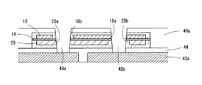
図5は、キャパシタ部品に形成する上部電極18と下部電極20の他の構成例を示す。図5(a)は断面図、図5(b)は上部電極18の平面図、図5(c)は下部電極20の平面図である。このキャパシタ部品33は、上部電極18と下部電極20の双方に、ビア径よりも大径となる開口穴18b、20bを配置したこと、開口穴18b、20bの平面配置位置が重複しないように配置したことを特徴とする。図示例では、上部電極18と下部電極20に2個ずつ対角配置に開口穴18b、20bを設けたが、開口穴18b、20bの配置位置、配置数は適宜選択することができる。
FIG. 5 shows another configuration example of the
(半導体パッケージ:第1の実施の形態)
上述したキャパシタ部品30〜33は、プリント基板等の基板に内蔵することによって、キャパシタ内蔵型の配線基板(半導体パッケージ)として提供することができる。
図6、7は、図2(b)に示したキャパシタ部品30を基板に内蔵して配線基板を形成する製造工程を示す。
図6(a)は、両面銅張り樹脂基板からなるコア基板40の上面の銅箔42を所定パターンにパターニングした状態を示す。銅箔42をパターニングする工程はコア基板40の両面に所定の配線パターンを形成する工程であり、図では、コア基板40の上面にキャパシタ部品30を搭載することを想定して配線パターン42aを形成した状態を示す。
図6(b)は、コア基板40の表面に樹脂フィルムをラミネートして層間絶縁層44を形成した状態を示す。
(Semiconductor package: first embodiment)
The
6 and 7 show a manufacturing process in which the
FIG. 6A shows a state in which the
FIG. 6B shows a state in which an
図6(c)、(d)は、コア基板40の上面にキャパシタ部品30を配置する工程である。キャパシタ部品30を層間絶縁層44の上に配置し、ビルドアップ用の樹脂フィルム46をコア基板40の上方からラミネートすることにより、層間絶縁層44、46aにキャパシタ部品30を埋没させるように配置する(図6(d))。キャパシタ部品30の被覆部24の外面が粗面に形成されていると、アンカー効果によって、層間絶縁層44、46aとキャパシタ部品30との密着性が向上するという利点がある。
FIGS. 6C and 6D are steps for disposing the
図7は、層間絶縁層44、46aに埋没して配置されたキャパシタ部品30の上部電極18および下部電極20と配線パターンとを層間で電気的に接続する工程を示す。
図7(a)は、キャパシタ部品30の配置位置に合わせて、ビア穴を形成する工程である。ビア穴48a、48bは、CO2レーザあるいはUV-YAGレーザ等を用いて、層間絶縁層46aの上方から、キャパシタ部品30に形成した開口穴18a、18b、20a、20bに位置合わせして形成する。層間絶縁層46a、44はレーザ加工によって容易に穴あけ加工することができ、誘電体層14もレーザ加工によって簡単に穴あけ加工できる。
FIG. 7 shows a process of electrically connecting the
FIG. 7A shows a process of forming a via hole in accordance with the arrangement position of the
前述したように、上部電極18と下部電極20には、小径の開口穴18a、20aと大径の開口穴18b、20bとが組み合わせて形成されている。
図8に、ビア穴48a、48bを形成した状態を拡大して示す。このビア穴加工においては、キャパシタ部品30を通過する部位でのビア穴の径を、小径の開口穴18a、20aよりも大径で、かつ大径の開口穴18b、20bよりも細径となるように設定する。
図8に示すビア穴48aは、上部電極18の開口穴18bが大径で、下部電極20の開口穴20aが小径である。したがって、ビア穴48aは、下部電極20と重複して交差し、上部電極18とは干渉しない配置となる。逆に、ビア穴48bは、上部電極18と重複して交差し、下部電極20とは干渉しない配置となる。
As described above, the
FIG. 8 is an enlarged view showing a state in which the via
In the via
このように、ビア穴を加工する際には、一方のビア穴が上部電極18と重複して交差し、他方のビア穴が下部電極20と重複して交差するように形成する。これによって、デカップリングキャパシタのプラス側の電極とマイナス側の電極に配線が別個に接続される。前述したように、キャパシタ部品の上部電極18と下部電極20には適宜開口穴を形成することができるから、ビア穴を形成する場合は、当該層における配線パターンの配置等を考慮し、適宜開口穴を選択してビア穴を形成すればよい。
As described above, when processing the via hole, one via hole overlaps the
図7(b)〜(c)は、キャパシタ部品30と電気的に接続する配線パターンを形成する工程である。
図7(b)は、ビア穴加工後、無電解銅めっき等によりめっきシード層50を形成し、レジストパターン52を形成した状態を示す。図は、キャパシタ部品30に接続する部分を示すが、レジストパターン52は、層間絶縁層46aの表面に形成する第2層目の配線パターンの全てのパターンにしたがってパターニングする。
図7(c)は、めっきシード層50をめっき給電層として電解銅めっきにより第2層目の配線パターン54を形成した状態を示す。
7B to 7C show a process of forming a wiring pattern that is electrically connected to the
FIG. 7B shows a state in which a
FIG. 7C shows a state in which the second-
図7(d)は、レジストパターン52を除去した後、めっきシード層50の露出部分を除去して、第2層目の配線パターン54を独立したパターンに形成した状態を示す。
第2層目の配線パターン54は下層の第1層目の配線パターン42aと、ビア54aを介して電気的に接続される。
また、キャパシタ部品30の上部電極18と下部電極20は、ビア54aを介して、一方と他方の配線パターン54にそれぞれ電気的に接続される。すなわち、配線パターン54の一方が、キャパシタ部品30の一方の極板である上部電極18に電気的に接続し、他方が、キャパシタ部品30の他方の極板である下部電極20に電気的に接続して、デカップリングキャパシタが基板に組み込まれる。
FIG. 7D shows a state in which, after the resist
The second-
Further, the
キャパシタ部品30を層間に搭載した後は、一般的なビルドアップ方法を利用して、配線パターンを多層に積層して配線基板を形成する。
本実施形態においては、コア基板40の直上にキャパシタ部品30を搭載したが、上記製造工程から明らかなように、キャパシタ部品30はコア基板40の直上に限らず、多層配線基板の任意の層間に搭載することが可能である。たとえば、多層配線基板に搭載される半導体チップの直下層に設けることで、半導体チップにより近接させて搭載することもできる。
また、基板の平面内におけるキャパシタ部品の配置位置も任意に選択することができ、同一平面内で複数個所に配置することもできる。また、複数層に個別にキャパシタ部品を搭載することもできる。
After the
In the present embodiment, the
In addition, the arrangement positions of the capacitor components in the plane of the substrate can be arbitrarily selected, and can be arranged at a plurality of locations in the same plane. In addition, capacitor components can be individually mounted on a plurality of layers.
(半導体パッケージ:第2の実施の形態)
図9は、図5に示したキャパシタ部品33を搭載した配線基板(半導体パッケージ)の例を示す。キャパシタ部品33は、上部電極18と下部電極20にそれぞれ大径の開口穴18b、20bのみを形成したものである。
このキャパシタ部品33を使用する場合も、図7、8に示したと同様な製造工程によってキャパシタ部品33を基板に内蔵させることができる。上述した配線基板の構造と本実施形態の配線基板の構造が相違する点は、キャパシタ部品33と配線パターン54とを電気的に接続するビア54aの構造である。
(Semiconductor package: second embodiment)
FIG. 9 shows an example of a wiring board (semiconductor package) on which the
Even when this
上述した実施形態においては、ビア穴48a、48bは上層の配線パターン54から下層の配線パターン42aにまで貫通するように形成した。これは、キャパシタ部品30に形成した開口穴18a〜20bに位置合わせしてビア54aを形成したからである。
これに対して、図5に示したキャパシタ部品33では、大径の開口穴18b、20bのみ形成され、小径の開口穴18a、20aが形成されていない。
したがって、キャパシタ部品33を層間絶縁層46a、44に埋設した状態でビア穴をあけると、上部電極18において開口穴18bを形成していない部位では、上部電極18の表面でビア穴が遮られる。また、上部電極18において、開口穴18bを形成した部位では、誘電体層14を通過して下部電極20の表面でビア穴が遮られる。
In the embodiment described above, the via
On the other hand, in the
Therefore, if a via hole is made with the
図9では、キャパシタ部品33において、開口穴18bを形成していない部位ではビア54bを介して配線パターン54と上部電極18とが電気的に接続されることを示す。また、キャパシタ部品33において開口穴18bを形成した部位では、ビア54cを介して下部電極20と配線パターン54とが電気的に接続されることを示す。
すなわち、本実施形態では、第2層に形成した配線パターン54との間で、キャパシタ部品33の上部電極18と下部電極20とが接続する構造となっている。この場合も、一方の配線パターン54がキャパシタ部品33の極板となる上部電極18に電気的に接続し、他方の配線パターン54がキャパシタ部品33の極板となる下部電極20に電気的に接続して、基板にデカップリングキャパシタが内蔵された構成となる。
FIG. 9 shows that in the
That is, in this embodiment, the
このように、基板にキャパシタ部品を搭載する場合に、キャパシタ部品を挟んで配置される配線層の一方の配線層と電気的に接続されるようにキャパシタ部品を搭載することもできるし、前述した実施形態のように、両方の配線層と電気的に接続されるようにキャパシタ部品を搭載することもできる。
なお、図9では、キャパシタ部品33を搭載する際に、上部電極18を上側として搭載したが、キャパシタ部品33の上下向きを反転させて、下部電極20を上側として搭載することも可能である。
本実施形態のように、ビア穴の内底面を上部電極18あるいは下部電極20の位置で止めるようにして配線パターンと上部電極18あるいは下部電極20とを電気的に接続する構成とする場合には、上部電極18あるいは下部電極20のいずれか一方に、ビア穴よりも大径となる開口穴を少なくとも一つ形成すればよい。
Thus, when mounting a capacitor component on a substrate, the capacitor component can be mounted so as to be electrically connected to one wiring layer of the wiring layers arranged with the capacitor component interposed therebetween, as described above. As in the embodiment, the capacitor component can be mounted so as to be electrically connected to both wiring layers.
In FIG. 9, when the
When the wiring pattern and the
(半導体パッケージ:第3の実施の形態)
図10は、誘電体層14を上部電極18と下部電極20とによって挟み、外面を樹脂からなる被覆部24によって被覆した構成を有するキャパシタシート体34を基板のコアとして配線基板(半導体パッケージ)を形成する例を示す。前述したキャパシタ部品30は両面を樹脂24aからなる被覆部によって被覆するから、被覆部24に所定の強度を付与することによって、コア基板として使用することが可能である。本実施形態においてはこのキャパシタシート体34を使用して配線基板を形成する。
図10(a)は、誘電体層14、上部電極18、下部電極20を備え、被覆部24によって外面を被覆したキャパシタシート体34である。このキャパシタシート体34は個片に切断してキャパシタ部品30を形成する前段階の状態のものである。
上部電極18に開口穴18a、18bを形成すること、下部電極20に開口穴20a、20bを形成する構成はキャパシタ部品30の構成と同様である。
(Semiconductor Package: Third Embodiment)
FIG. 10 shows a wiring board (semiconductor package) with a
FIG. 10A shows a
The configuration of forming the opening holes 18 a and 18 b in the
図10(b)は、キャパシタシート体34に、シート体を厚さ方向に貫通する貫通孔60を形成した状態を示す。貫通孔60はレーザ加工あるいはドリル加工によって形成することができる。貫通孔60は、一方が上部電極18と重複して交差し、他方が下部電極20と重複して交差するように、形成位置および径寸法を制御して形成する。
図10(c)は、シート体の両面に電解銅めっきを施し、貫通孔60をめっき銅62によって充填し、同時にシート体の両面に銅層64を形成した状態を示す。
FIG. 10B shows a state in which a through
FIG. 10C shows a state in which electrolytic copper plating is performed on both surfaces of the sheet body, the through
次いで、シート体の両面にレジストパターン66を形成する(図10(d))。レジストパターン66はシート体の両面に被着する銅層64をパターニングして配線パターンを形成するためのものである。
図10(e)は、レジストパターン66をマスクとして銅層64をパターニングし、その後、レジストパターン66を除去した状態を示す。シート体の両面に配線パターン64a、64bが形成されたことを示す。
図10(f)は外部接続端子を接合するパッドを形成するため、シート体の両面に感光性のソルダーレジストを塗布し、パッドを形成する部位を露出させるようにソルダーレジスト68をパターニングした状態である。シート体の上面に形成された配線パターン64aにパッド65aが形成され、シート体の下面にパッド65bが形成される。
Next, a resist
FIG. 10E shows a state in which the
FIG. 10 (f) shows a state in which a photosensitive solder resist is applied to both sides of the sheet body to form pads for joining the external connection terminals, and the solder resist 68 is patterned so as to expose the portions where the pads are to be formed. is there.
ソルダーレジスト68をパターニングするとパッド65a、65bの部分で銅層が露出するから、パッド65a、65b部分に、保護めっきとしてニッケルめっきと、金めっきをこの順に施す。
図10(g)は、パッド65a、65bに外部接続端子70a、70bとしてはんだボールを接合した状態を示す。外部接続端子70a、70bを接合する工程は、パッド65a、65bにはんだ印刷によってはんだを供給し、はんだボールを搭載し、はんだリフローによる。
本実施形態では大判のシート体を使用しているから、はんだリフロー工程では、個片状あるいは短冊状にシート体を切断して外部接続端子70a、70bを接合する。
When the solder resist 68 is patterned, the copper layer is exposed at the
FIG. 10G shows a state where solder balls are joined to the
In this embodiment, since a large sheet is used, in the solder reflow process, the sheet is cut into pieces or strips and the
こうして、コア基板自体にデカップリングキャパシタを内蔵し、キャパシタの上部電極18および下部電極20と基板の表面に形成した配線パターンとが電気的に接続された構造を有する配線基板を得ることができる。
図10(g)に示す配線基板は、基板に内蔵されるキャパシタの部分の断面を示すが、上述した製造工程は、コア基板を用いる両面配線基板の製造工程と基本的に変わらない。すなわち、上述した製造工程において、キャパシタに接続される配線パターンに加えて、配線基板の両面に所要の配線パターンを形成することによって、一般に用いられている両面配線基板と同様の構成を備える配線基板(半導体パッケージ)が得られる。
In this way, it is possible to obtain a wiring substrate having a structure in which a decoupling capacitor is built in the core substrate itself and the
The wiring board shown in FIG. 10 (g) shows a cross section of the capacitor portion built in the board, but the above-described manufacturing process is basically the same as the manufacturing process of the double-sided wiring board using the core board. That is, in the manufacturing process described above, in addition to the wiring pattern connected to the capacitor, a wiring board having the same configuration as a commonly used double-sided wiring board is formed by forming a required wiring pattern on both surfaces of the wiring board. (Semiconductor package) is obtained.
図11は、上述した製造方法によって得られた配線基板72に半導体素子80を搭載して、2段に配線基板を積み重ねて形成した半導体パッケージ(POP:Package on Package)を構成した例を示す。配線基板72にはデカップリングキャパシタが内蔵されている。上段の配線基板74についてもデカップリングキャパシタを内蔵した基板を用いてもよい。外部接続端子70aを大径に形成したことによって、配線基板72、74間に半導体素子80を搭載するスペースを確保している。
FIG. 11 shows an example in which a semiconductor package (POP: Package on Package) is formed by mounting the
本実施形態の半導体装置のように、基板内にデカップリングキャパシタを内蔵させることにより、電源電位を安定させるといったことが可能となる。デカップリングキャパシタを内蔵した配線基板は、POP型の半導体パッケージのように積層型とした場合にも、薄型化を図ることができる。また、POP型に限らず、単一の配線基板を用いた半導体パッケージとして構成することももちろん可能である。 As in the semiconductor device of the present embodiment, the power supply potential can be stabilized by incorporating a decoupling capacitor in the substrate. A wiring board with a built-in decoupling capacitor can be thinned even when it is a laminated type like a POP type semiconductor package. Of course, the semiconductor package is not limited to the POP type, and can be configured as a semiconductor package using a single wiring board.
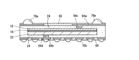
図12は、誘電体層14を上部電極18と下部電極20とによって挟み、樹脂24aからなる被覆部24によって外面を保護するキャパシタ構造をコア基板に利用する他の例である。この例では、上部電極18と下部電極20には開口穴を設けず、基板の両面に形成した配線パターン64a、64bと上部電極18および下部電極20とを、ビア64c、64dを介して電気的に接続している。基板の両面に形成される配線パターン64a、64b間の電気的接続は、従来の両面配線基板と同様に基板に設けるスルーホールを介してなされる。この構造の半導体パッケージの場合は、基板に内蔵するキャパシタ構造に用いる上部電極18と下部電極20を、開口穴を設けない単一膜構造とすることができる。
なお、コア基板にキャパシタ構造を組み込む方法としては、図9に示すような、基板の一方の面側から、配線パターンと上部電極18および下部電極20とを電気的に接続する構成とすることもできる。
FIG. 12 shows another example in which a capacitor structure in which the
In addition, as a method of incorporating the capacitor structure into the core substrate, a configuration in which the wiring pattern and the
本発明に係るキャパシタ部品あるいはキャパシタ構造を内蔵した配線基板(半導体パッケージ)は、誘電体層14を上部電極18と下部電極20とで挟む構造としているから、誘電体層14の大きさ、言い換えれば上部電極18と下部電極20の大きさを大きくすることによってより大きな電気容量を確保することが可能である。また、誘電体層14、上部電極18、下部電極20を積層した構造としたことにより、薄型化、小型化が図れ、ビルドアップ層に組み込んでキャパシタ内蔵型の配線基板を形成するといったことが容易に可能になる。また、上部電極18および下部電極20は任意のパターンに形成できるから、キャパシタ部品を組み込む製品に応じて電極のパターンや開口穴のパターンを適宜設計することが可能になる等の利点を有する。
Since the wiring board (semiconductor package) incorporating the capacitor component or capacitor structure according to the present invention has a structure in which the
10 キャパシタシート
12 ニッケル層
14 誘電体層
16 銅箔
16a 銅めっき層
18 上部電極
18a、18b、20a、20b 開口穴
20 下部電極
22 銅板
24a 樹脂
24 被覆部
30、31、32、33 キャパシタ部品
34 キャパシタシート体
40 コア基板
42 銅箔
42a 配線パターン
44、46a 層間絶縁層
46 樹脂フィルム
48a、48b ビア穴
50 めっきシード層
52 レジストパターン
54 配線パターン
54a、54b、54c ビア
60 貫通孔
64a、64b 配線パターン
65a、65b パッド
66 レジストパターン
68 ソルダーレジスト
70a、70b 外部接続端子
72、74 配線基板
80 半導体素子
DESCRIPTION OF
Claims (1)
前記金属層と前記支持層を所定パターンにエッチングし、それぞれ上部電極と下部電極として形成する工程と、
絶縁樹脂が被着した板を用い、前記絶縁樹脂が被着した面を前記キャパシタシートに向け、前記板を加熱および加圧して、前記上部電極と下部電極が形成された前記キャパシタシートの両面に前記絶縁樹脂を圧着した後、前記板を除去して、前記キャパシタシートの面を前記絶縁樹脂により被覆する工程と、
前記絶縁樹脂による被覆部が形成された前記キャパシタシートを個片のキャパシタ部品に切断する工程とを備え、
前記板は、前記絶縁樹脂が被着する面が粗面に形成され、
前記板を除去することにより、前記絶縁樹脂による前記被覆部の外面が粗面に形成されることを特徴とするキャパシタ部品の製造方法。 A method of manufacturing a capacitor component using a capacitor sheet formed by laminating a dielectric layer on a surface of a support layer made of metal and laminating a metal layer on the dielectric layer,
Etching the metal layer and the support layer into a predetermined pattern to form an upper electrode and a lower electrode, respectively;
Using a plate coated with an insulating resin, with the surface coated with the insulating resin facing the capacitor sheet, and heating and pressing the plate, both sides of the capacitor sheet on which the upper electrode and the lower electrode are formed After crimping the insulating resin, removing the plate and coating the surface of the capacitor sheet with the insulating resin;
Cutting the capacitor sheet formed with the insulating resin covering portion into individual capacitor components,
The plate has a rough surface on which the insulating resin adheres,
By removing the plate, the outer surface of the covering portion made of the insulating resin is formed into a rough surface.
Priority Applications (2)
| Application Number | Priority Date | Filing Date | Title |
|---|---|---|---|
| JP2008118519A JP5188256B2 (en) | 2008-04-30 | 2008-04-30 | Capacitor component manufacturing method |
| US12/431,937 US20090273884A1 (en) | 2008-04-30 | 2009-04-29 | Capacitor component, method of manufacturing the same and semiconductor package |
Applications Claiming Priority (1)
| Application Number | Priority Date | Filing Date | Title |
|---|---|---|---|
| JP2008118519A JP5188256B2 (en) | 2008-04-30 | 2008-04-30 | Capacitor component manufacturing method |
Publications (3)
| Publication Number | Publication Date |
|---|---|
| JP2009267310A JP2009267310A (en) | 2009-11-12 |
| JP2009267310A5 JP2009267310A5 (en) | 2011-03-10 |
| JP5188256B2 true JP5188256B2 (en) | 2013-04-24 |
Family
ID=41256937
Family Applications (1)
| Application Number | Title | Priority Date | Filing Date |
|---|---|---|---|
| JP2008118519A Active JP5188256B2 (en) | 2008-04-30 | 2008-04-30 | Capacitor component manufacturing method |
Country Status (2)
| Country | Link |
|---|---|
| US (1) | US20090273884A1 (en) |
| JP (1) | JP5188256B2 (en) |
Cited By (1)
| Publication number | Priority date | Publication date | Assignee | Title |
|---|---|---|---|---|
| KR20180076135A (en) * | 2016-12-27 | 2018-07-05 | 한국제이씨씨(주) | Method of manufacturing porous current collector |
Families Citing this family (18)
| Publication number | Priority date | Publication date | Assignee | Title |
|---|---|---|---|---|
| US7856265B2 (en) * | 2007-02-22 | 2010-12-21 | Cardiac Pacemakers, Inc. | High voltage capacitor route with integrated failure point |
| US8725252B2 (en) | 2009-12-18 | 2014-05-13 | Cardiac Pacemakers, Inc. | Electric energy storage device electrode including an overcurrent protector |
| US9129749B2 (en) | 2009-12-18 | 2015-09-08 | Cardiac Pacemakers, Inc. | Sintered electrodes to store energy in an implantable medical device |
| US8873220B2 (en) | 2009-12-18 | 2014-10-28 | Cardiac Pacemakers, Inc. | Systems and methods to connect sintered aluminum electrodes of an energy storage device |
| US9123470B2 (en) | 2009-12-18 | 2015-09-01 | Cardiac Pacemakers, Inc. | Implantable energy storage device including a connection post to connect multiple electrodes |
| US8619408B2 (en) | 2009-12-18 | 2013-12-31 | Cardiac Pacemakers, Inc. | Sintered capacitor electrode including a folded connection |
| WO2011075511A2 (en) | 2009-12-18 | 2011-06-23 | Cardiac Pacemakers, Inc. | Sintered capacitor electrode including multiple thicknesses |
| JP5429019B2 (en) * | 2010-04-16 | 2014-02-26 | 富士通株式会社 | Capacitor and manufacturing method thereof |
| US8848341B2 (en) | 2010-06-24 | 2014-09-30 | Cardiac Pacemakers, Inc. | Electronic component mounted on a capacitor electrode |
| TWI446497B (en) * | 2010-08-13 | 2014-07-21 | Unimicron Technology Corp | Package substrate having a passive element embedded therein and fabrication method thereof |
| JP2015095587A (en) * | 2013-11-13 | 2015-05-18 | 日本特殊陶業株式会社 | Multilayer wiring board |
| WO2016094140A1 (en) * | 2014-12-10 | 2016-06-16 | Suzhou Qing Xin Fang Electronics Technology Co., Ltd. | Methods and devices of laminated integrations of semiconductor chips, magnetics, and capacitance |
| WO2017154167A1 (en) * | 2016-03-10 | 2017-09-14 | 三井金属鉱業株式会社 | Multilayer laminate plate and production method for multilayered printed wiring board using same |
| DE102016106284A1 (en) | 2016-04-06 | 2017-10-12 | Epcos Ag | module |
| WO2017183146A1 (en) | 2016-04-21 | 2017-10-26 | 富士通株式会社 | Circuit board, method for manufacturing circuit board, and electronic device |
| CN107622950A (en) * | 2016-07-13 | 2018-01-23 | 欣兴电子股份有限公司 | Package substrate and its manufacture method |
| US10141277B2 (en) | 2017-03-31 | 2018-11-27 | International Business Machines Corporation | Monolithic decoupling capacitor between solder bumps |
| US11195805B2 (en) * | 2018-03-30 | 2021-12-07 | Intel Corporation | Capacitor die embedded in package substrate for providing capacitance to surface mounted die |
Family Cites Families (8)
| Publication number | Priority date | Publication date | Assignee | Title |
|---|---|---|---|---|
| USRE41242E1 (en) * | 1997-10-17 | 2010-04-20 | Ibiden Co., Ltd. | Package substrate |
| JPH11284342A (en) * | 1998-03-31 | 1999-10-15 | Sumitomo Metal Ind Ltd | Package and manufacture thereof |
| JP3197540B2 (en) * | 1999-02-05 | 2001-08-13 | ソニーケミカル株式会社 | Substrate piece and flexible substrate |
| JP4211210B2 (en) * | 2000-09-08 | 2009-01-21 | 日本電気株式会社 | Capacitor, mounting structure thereof, manufacturing method thereof, semiconductor device and manufacturing method thereof |
| JP4447881B2 (en) * | 2003-10-14 | 2010-04-07 | 富士通株式会社 | Manufacturing method of interposer |
| JP4649198B2 (en) * | 2004-12-20 | 2011-03-09 | 新光電気工業株式会社 | Wiring board manufacturing method |
| JP4351148B2 (en) * | 2004-12-28 | 2009-10-28 | 新光電気工業株式会社 | Wiring board manufacturing method |
| KR100966638B1 (en) * | 2008-03-25 | 2010-06-29 | 삼성전기주식회사 | Printed circuit board having capacitor and manufacturing method thereof |
-
2008
- 2008-04-30 JP JP2008118519A patent/JP5188256B2/en active Active
-
2009
- 2009-04-29 US US12/431,937 patent/US20090273884A1/en not_active Abandoned
Cited By (1)
| Publication number | Priority date | Publication date | Assignee | Title |
|---|---|---|---|---|
| KR20180076135A (en) * | 2016-12-27 | 2018-07-05 | 한국제이씨씨(주) | Method of manufacturing porous current collector |
Also Published As
| Publication number | Publication date |
|---|---|
| US20090273884A1 (en) | 2009-11-05 |
| JP2009267310A (en) | 2009-11-12 |
Similar Documents
| Publication | Publication Date | Title |
|---|---|---|
| JP5188256B2 (en) | Capacitor component manufacturing method | |
| US6333857B1 (en) | Printing wiring board, core substrate, and method for fabricating the core substrate | |
| KR100773287B1 (en) | Multi-layer substrate | |
| US8510936B2 (en) | Manufacturing method of package carrier | |
| EP2768291B1 (en) | Component built-in board and method of manufacturing the same, and mounting body | |
| US20090097218A1 (en) | Capacitor-embedded printed wiring board and method of manufacturing the same | |
| JP2000323645A (en) | Semiconductor device and manufacture thereof | |
| JP2005045013A (en) | Circuit module and its manufacturing method | |
| KR20070112702A (en) | Electronic device substrate, electronic device and methods for fabricating the same | |
| JP2008288298A (en) | Method for manufacturing printed-wiring board with built-in electronic part | |
| JP2008159973A (en) | Electronic component module and circuit board with built-in components incorporating the module | |
| JP5462450B2 (en) | Component built-in printed wiring board and method for manufacturing component built-in printed wiring board | |
| KR101905879B1 (en) | The printed circuit board and the method for manufacturing the same | |
| US20150351218A1 (en) | Component built-in board and method of manufacturing the same, and mounting body | |
| JP4863076B2 (en) | Wiring board and manufacturing method thereof | |
| JP6315681B2 (en) | Component-embedded substrate, manufacturing method thereof, and mounting body | |
| TWI752202B (en) | Support attached printed circuit board and manufacturing method therof | |
| US9826646B2 (en) | Component built-in board and method of manufacturing the same, and mounting body | |
| JP5913535B1 (en) | Component built-in substrate and manufacturing method thereof | |
| KR100653247B1 (en) | Printed circuit board having embedded electric components and fabricating method therefore | |
| JP4467341B2 (en) | Manufacturing method of multilayer wiring board | |
| JP4795860B2 (en) | Capacitor, wiring board | |
| JP2007189202A (en) | Manufacturing method of circuit board | |
| JP2005101377A (en) | Multilayer wiring board | |
| JP2008147228A (en) | Wiring board and its manufacturing method |
Legal Events
| Date | Code | Title | Description |
|---|---|---|---|
| A521 | Written amendment |
Free format text: JAPANESE INTERMEDIATE CODE: A523 Effective date: 20110125 |
|
| A621 | Written request for application examination |
Free format text: JAPANESE INTERMEDIATE CODE: A621 Effective date: 20110125 |
|
| A977 | Report on retrieval |
Free format text: JAPANESE INTERMEDIATE CODE: A971007 Effective date: 20120209 |
|
| A131 | Notification of reasons for refusal |
Free format text: JAPANESE INTERMEDIATE CODE: A131 Effective date: 20120221 |
|
| A521 | Written amendment |
Free format text: JAPANESE INTERMEDIATE CODE: A523 Effective date: 20120404 |
|
| A131 | Notification of reasons for refusal |
Free format text: JAPANESE INTERMEDIATE CODE: A131 Effective date: 20121106 |
|
| A521 | Written amendment |
Free format text: JAPANESE INTERMEDIATE CODE: A523 Effective date: 20121207 |
|
| TRDD | Decision of grant or rejection written | ||
| A01 | Written decision to grant a patent or to grant a registration (utility model) |
Free format text: JAPANESE INTERMEDIATE CODE: A01 Effective date: 20130115 |
|
| A61 | First payment of annual fees (during grant procedure) |
Free format text: JAPANESE INTERMEDIATE CODE: A61 Effective date: 20130122 |
|
| FPAY | Renewal fee payment (event date is renewal date of database) |
Free format text: PAYMENT UNTIL: 20160201 Year of fee payment: 3 |
|
| R150 | Certificate of patent or registration of utility model |
Ref document number: 5188256 Country of ref document: JP Free format text: JAPANESE INTERMEDIATE CODE: R150 Free format text: JAPANESE INTERMEDIATE CODE: R150 |