JP5164107B2 - プラズマcvd装置、薄膜の製造方法及び磁気記録媒体の製造方法 - Google Patents
プラズマcvd装置、薄膜の製造方法及び磁気記録媒体の製造方法 Download PDFInfo
- Publication number
- JP5164107B2 JP5164107B2 JP2008172489A JP2008172489A JP5164107B2 JP 5164107 B2 JP5164107 B2 JP 5164107B2 JP 2008172489 A JP2008172489 A JP 2008172489A JP 2008172489 A JP2008172489 A JP 2008172489A JP 5164107 B2 JP5164107 B2 JP 5164107B2
- Authority
- JP
- Japan
- Prior art keywords
- chamber
- electrode
- ring
- plasma cvd
- plasma
- Prior art date
- Legal status (The legal status is an assumption and is not a legal conclusion. Google has not performed a legal analysis and makes no representation as to the accuracy of the status listed.)
- Expired - Fee Related
Links
- 238000005268 plasma chemical vapour deposition Methods 0.000 title claims description 52
- 238000004519 manufacturing process Methods 0.000 title claims description 21
- 239000010409 thin film Substances 0.000 title claims description 19
- 239000000758 substrate Substances 0.000 claims description 64
- 239000010408 film Substances 0.000 claims description 56
- 230000007246 mechanism Effects 0.000 claims description 22
- 238000000151 deposition Methods 0.000 claims description 18
- 230000008021 deposition Effects 0.000 claims description 18
- 230000015572 biosynthetic process Effects 0.000 claims description 15
- 238000010438 heat treatment Methods 0.000 claims description 15
- OKTJSMMVPCPJKN-UHFFFAOYSA-N Carbon Chemical compound [C] OKTJSMMVPCPJKN-UHFFFAOYSA-N 0.000 claims description 11
- 229910052799 carbon Inorganic materials 0.000 claims description 9
- 229910052710 silicon Inorganic materials 0.000 claims description 4
- 239000010703 silicon Substances 0.000 claims description 4
- 239000010410 layer Substances 0.000 claims description 3
- 239000011241 protective layer Substances 0.000 claims description 3
- 238000009616 inductively coupled plasma Methods 0.000 description 95
- 239000007789 gas Substances 0.000 description 78
- 210000002381 plasma Anatomy 0.000 description 59
- 239000003990 capacitor Substances 0.000 description 30
- 238000005229 chemical vapour deposition Methods 0.000 description 20
- 238000012986 modification Methods 0.000 description 14
- 230000004048 modification Effects 0.000 description 14
- 238000010586 diagram Methods 0.000 description 10
- 238000000034 method Methods 0.000 description 9
- 230000001133 acceleration Effects 0.000 description 8
- 238000001816 cooling Methods 0.000 description 7
- 230000008878 coupling Effects 0.000 description 5
- 238000010168 coupling process Methods 0.000 description 5
- 238000005859 coupling reaction Methods 0.000 description 5
- 229910004298 SiO 2 Inorganic materials 0.000 description 4
- 238000004140 cleaning Methods 0.000 description 4
- 238000012937 correction Methods 0.000 description 4
- FFUAGWLWBBFQJT-UHFFFAOYSA-N hexamethyldisilazane Chemical compound C[Si](C)(C)N[Si](C)(C)C FFUAGWLWBBFQJT-UHFFFAOYSA-N 0.000 description 4
- MYMOFIZGZYHOMD-UHFFFAOYSA-N Dioxygen Chemical compound O=O MYMOFIZGZYHOMD-UHFFFAOYSA-N 0.000 description 3
- QVGXLLKOCUKJST-UHFFFAOYSA-N atomic oxygen Chemical compound [O] QVGXLLKOCUKJST-UHFFFAOYSA-N 0.000 description 3
- 229910001882 dioxygen Inorganic materials 0.000 description 3
- 230000005684 electric field Effects 0.000 description 3
- 239000001301 oxygen Substances 0.000 description 3
- 229910052760 oxygen Inorganic materials 0.000 description 3
- 239000002245 particle Substances 0.000 description 3
- 230000008569 process Effects 0.000 description 3
- 239000002994 raw material Substances 0.000 description 3
- 239000004020 conductor Substances 0.000 description 2
- 229910003460 diamond Inorganic materials 0.000 description 2
- 239000010432 diamond Substances 0.000 description 2
- 229910002804 graphite Inorganic materials 0.000 description 2
- 239000010439 graphite Substances 0.000 description 2
- 150000002500 ions Chemical class 0.000 description 2
- 238000012423 maintenance Methods 0.000 description 2
- 238000005259 measurement Methods 0.000 description 2
- 150000003377 silicon compounds Chemical class 0.000 description 2
- 125000006850 spacer group Chemical group 0.000 description 2
- GUVRBAGPIYLISA-UHFFFAOYSA-N tantalum atom Chemical compound [Ta] GUVRBAGPIYLISA-UHFFFAOYSA-N 0.000 description 2
- XLYOFNOQVPJJNP-UHFFFAOYSA-N water Substances O XLYOFNOQVPJJNP-UHFFFAOYSA-N 0.000 description 2
- DXLXRNZCYAYUED-UHFFFAOYSA-N 4-[2-[4-(3-quinolin-4-ylpyrazolo[1,5-a]pyrimidin-6-yl)phenoxy]ethyl]morpholine Chemical compound C=1C=C(C2=CN3N=CC(=C3N=C2)C=2C3=CC=CC=C3N=CC=2)C=CC=1OCCN1CCOCC1 DXLXRNZCYAYUED-UHFFFAOYSA-N 0.000 description 1
- 239000004215 Carbon black (E152) Substances 0.000 description 1
- RYGMFSIKBFXOCR-UHFFFAOYSA-N Copper Chemical compound [Cu] RYGMFSIKBFXOCR-UHFFFAOYSA-N 0.000 description 1
- 230000002159 abnormal effect Effects 0.000 description 1
- 230000032683 aging Effects 0.000 description 1
- 238000013459 approach Methods 0.000 description 1
- 238000004380 ashing Methods 0.000 description 1
- 238000006243 chemical reaction Methods 0.000 description 1
- 229910052802 copper Inorganic materials 0.000 description 1
- 239000010949 copper Substances 0.000 description 1
- 230000007423 decrease Effects 0.000 description 1
- 230000002950 deficient Effects 0.000 description 1
- 238000001514 detection method Methods 0.000 description 1
- 238000009826 distribution Methods 0.000 description 1
- 235000012489 doughnuts Nutrition 0.000 description 1
- 230000000694 effects Effects 0.000 description 1
- 238000007542 hardness measurement Methods 0.000 description 1
- UQEAIHBTYFGYIE-UHFFFAOYSA-N hexamethyldisiloxane Chemical compound C[Si](C)(C)O[Si](C)(C)C UQEAIHBTYFGYIE-UHFFFAOYSA-N 0.000 description 1
- 229930195733 hydrocarbon Natural products 0.000 description 1
- 150000002430 hydrocarbons Chemical class 0.000 description 1
- 230000001939 inductive effect Effects 0.000 description 1
- 239000012212 insulator Substances 0.000 description 1
- 239000007788 liquid Substances 0.000 description 1
- 229910052751 metal Inorganic materials 0.000 description 1
- 239000002184 metal Substances 0.000 description 1
- 238000009832 plasma treatment Methods 0.000 description 1
- 238000012545 processing Methods 0.000 description 1
- 238000003892 spreading Methods 0.000 description 1
- 230000007480 spreading Effects 0.000 description 1
- 229910052715 tantalum Inorganic materials 0.000 description 1
- 230000008016 vaporization Effects 0.000 description 1
Images


Classifications
-
- G—PHYSICS
- G11—INFORMATION STORAGE
- G11B—INFORMATION STORAGE BASED ON RELATIVE MOVEMENT BETWEEN RECORD CARRIER AND TRANSDUCER
- G11B5/00—Recording by magnetisation or demagnetisation of a record carrier; Reproducing by magnetic means; Record carriers therefor
- G11B5/84—Processes or apparatus specially adapted for manufacturing record carriers
- G11B5/851—Coating a support with a magnetic layer by sputtering
-
- C—CHEMISTRY; METALLURGY
- C23—COATING METALLIC MATERIAL; COATING MATERIAL WITH METALLIC MATERIAL; CHEMICAL SURFACE TREATMENT; DIFFUSION TREATMENT OF METALLIC MATERIAL; COATING BY VACUUM EVAPORATION, BY SPUTTERING, BY ION IMPLANTATION OR BY CHEMICAL VAPOUR DEPOSITION, IN GENERAL; INHIBITING CORROSION OF METALLIC MATERIAL OR INCRUSTATION IN GENERAL
- C23C—COATING METALLIC MATERIAL; COATING MATERIAL WITH METALLIC MATERIAL; SURFACE TREATMENT OF METALLIC MATERIAL BY DIFFUSION INTO THE SURFACE, BY CHEMICAL CONVERSION OR SUBSTITUTION; COATING BY VACUUM EVAPORATION, BY SPUTTERING, BY ION IMPLANTATION OR BY CHEMICAL VAPOUR DEPOSITION, IN GENERAL
- C23C16/00—Chemical coating by decomposition of gaseous compounds, without leaving reaction products of surface material in the coating, i.e. chemical vapour deposition [CVD] processes
- C23C16/44—Chemical coating by decomposition of gaseous compounds, without leaving reaction products of surface material in the coating, i.e. chemical vapour deposition [CVD] processes characterised by the method of coating
- C23C16/50—Chemical coating by decomposition of gaseous compounds, without leaving reaction products of surface material in the coating, i.e. chemical vapour deposition [CVD] processes characterised by the method of coating using electric discharges
- C23C16/505—Chemical coating by decomposition of gaseous compounds, without leaving reaction products of surface material in the coating, i.e. chemical vapour deposition [CVD] processes characterised by the method of coating using electric discharges using radio frequency discharges
- C23C16/509—Chemical coating by decomposition of gaseous compounds, without leaving reaction products of surface material in the coating, i.e. chemical vapour deposition [CVD] processes characterised by the method of coating using electric discharges using radio frequency discharges using internal electrodes
-
- H—ELECTRICITY
- H01—ELECTRIC ELEMENTS
- H01J—ELECTRIC DISCHARGE TUBES OR DISCHARGE LAMPS
- H01J37/00—Discharge tubes with provision for introducing objects or material to be exposed to the discharge, e.g. for the purpose of examination or processing thereof
- H01J37/32—Gas-filled discharge tubes
- H01J37/32009—Arrangements for generation of plasma specially adapted for examination or treatment of objects, e.g. plasma sources
- H01J37/32082—Radio frequency generated discharge
- H01J37/321—Radio frequency generated discharge the radio frequency energy being inductively coupled to the plasma
-
- H—ELECTRICITY
- H01—ELECTRIC ELEMENTS
- H01J—ELECTRIC DISCHARGE TUBES OR DISCHARGE LAMPS
- H01J37/00—Discharge tubes with provision for introducing objects or material to be exposed to the discharge, e.g. for the purpose of examination or processing thereof
- H01J37/32—Gas-filled discharge tubes
- H01J37/32009—Arrangements for generation of plasma specially adapted for examination or treatment of objects, e.g. plasma sources
- H01J37/32082—Radio frequency generated discharge
- H01J37/32137—Radio frequency generated discharge controlling of the discharge by modulation of energy
- H01J37/32155—Frequency modulation
- H01J37/32165—Plural frequencies
-
- H—ELECTRICITY
- H01—ELECTRIC ELEMENTS
- H01J—ELECTRIC DISCHARGE TUBES OR DISCHARGE LAMPS
- H01J37/00—Discharge tubes with provision for introducing objects or material to be exposed to the discharge, e.g. for the purpose of examination or processing thereof
- H01J37/32—Gas-filled discharge tubes
- H01J37/32009—Arrangements for generation of plasma specially adapted for examination or treatment of objects, e.g. plasma sources
- H01J37/32082—Radio frequency generated discharge
- H01J37/32174—Circuits specially adapted for controlling the RF discharge
Landscapes
- Chemical & Material Sciences (AREA)
- Engineering & Computer Science (AREA)
- Physics & Mathematics (AREA)
- Plasma & Fusion (AREA)
- Analytical Chemistry (AREA)
- Materials Engineering (AREA)
- Chemical Kinetics & Catalysis (AREA)
- Mechanical Engineering (AREA)
- Metallurgy (AREA)
- Organic Chemistry (AREA)
- General Chemical & Material Sciences (AREA)
- Chemical Vapour Deposition (AREA)
- Manufacturing Of Magnetic Record Carriers (AREA)
- Plasma Technology (AREA)
Description
前記チャンバー内に配置されたリング状電極と、
前記リング状電極に電気的に接続された第1の高周波電源と、
前記チャンバー内に原料ガスを供給するガス供給機構と、
前記チャンバー内を排気する排気機構と、
前記チャンバー内に配置され、前記リング状電極に対向するように配置された被成膜基板と、
前記被成膜基板に電気的に接続された第2の高周波電源又はDC電源と、
前記チャンバー内に配置され、前記リング状電極に対向し且つ前記被成膜基板とは逆側に配置されたアース電極と、
前記チャンバー内に配置され、前記リング状電極と前記被成膜基板との間の空間を囲むように設けられたプラズマウォールと、
を具備し、
前記プラズマウォールがフロート電位とされていることを特徴とする。
なお、前記リング状電極はICP電極であることが好ましい。
また、本発明に係るプラズマCVD装置において、前記リング状電極とそのリング外面と対向する前記チャンバーの内面との間隔は5mm以下であることが好ましい。
また、本発明に係るプラズマCVD装置において、前記第1の高周波電源は1MHz〜27MHzの周波数を有し、前記第2の高周波電源は100〜500kHz以下の周波数を有することが好ましい。
前記チャンバー内に被成膜基板を配置し、
前記リング状電極と前記アース電極との間の放電によって前記原料ガスをプラズマ状態とすることにより、前記被成膜基板の表面に薄膜を形成することを特徴とする。
非磁性基板上に少なくとも磁性層を形成した被成膜基板を前記チャンバー内に配置し、
前記チャンバー内で前記リング状電極と前記アース電極との間の放電により前記原料ガスをプラズマ状態とし、このプラズマを前記被成膜基板の表面に加速衝突させて炭素が主成分である保護層を形成することを特徴とする。
(実施の形態1)
図1は、本発明の実施の形態1によるプラズマCVD装置の全体構成を示す模式図である。図2は、図1に示すチャンバー1の左側半分を拡大した断面図である。図3は、図1に示すICP電極(1ターンコイル)の斜視図である。図4は、図1に示すガス吐出リング及びヒータの断面図である。図5は、図1に示すマグネットの断面図である。図6は、図1に示すICP電極の断面図である。
また、同様に、ディスク基板2の他方の主面に対向する側(図1の右側)には前記ICP電極17と同様のICP電極18が配置されている。
また、同様に、ディスク基板2とICP電極18との間にプラズマウォール25が配置されている。
ガス : C7H8
ガス流量 : 2.8sccm
外部磁場 : 100G(ガウス)
ICP電源 : 300W
パルスバイアス : 450V
圧力 : 0.15Pa
成膜速度 : 0.5nm/分
ヌープ硬度(HK) : 2916(5点の平均値)
DLC膜の分布 : 良い
装置 : 松沢精機製 微小硬度計 DMH−2型
圧子 : 対稜角 172.5°,130° 菱形ダイアモンド四角錐圧子
加重 : 5g
加重時間 : 15秒
計測ポイント : サンプル上任意5点
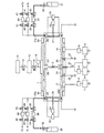
図9は、変形例1を説明するための模式図である。
ICP電極17,18それぞれの出力端Aは、マッチングボックス62を介してICP電源63に電気的に接続されている。また、ICP電極17,18それぞれの出力端Bは、共振コンデンサ64を介して接地電位に接続されている。この共振コンデンサ64は、ICP電源63から出力される高周波電流の周波数及びICP電極17,18のインダクタンスに対して共振条件又は共振条件の許容動作範囲を満たす容量を有している。
(1)ICP電極の浮遊容量が極めて小さく、放電初期に起こる容量結合放電(CCD:capacitive coupling discharge)が殆ど無視でき、誘導結合放電(ICD:inductive coupling discharge)によってプラズマが作られる。このため、プラズマは安定であり、高密度である。
(2)ICP電極と生成プラズマの磁気的結合が強く、上記共振回路のQ値(後述する)は低く、回路定数の許容誤差は緩く、単純な回路であるにも関わらず、回路の動作は安定で、運転が容易である。
ω=2πf=(LC)−1/2 ・・・(1)
C=1/(2πf)2L ・・・(2)
従って、共振条件を達成する共振コンデンサの容量Cは、1/(2πf)2Lに設定する必要がある。
ln2π+lnf=−1/2(lnL+lnC)
両辺の微分を取ると、
δf/f=−1/2(δL/L+δC/C)
両辺の絶対値を取ると、右辺の符号は+になる。
従って、δL/L=δC/C=0.1とすれば、
δf/f=0.1となり、これはQ値10に相当する。
それ故、ICP電極とコンデンサの誤差は最大で10%まで許される。
0.9/(2πf)2L≦C≦1.1/(2πf)2L ・・・(3)
0.95/(2πf)2L≦C≦1.05/(2πf)2L ・・・(4)
C=1/(6.28×13.56×E6)2×1×E−6
=1.38×10⁻¹⁰(farad)
=138pF
C(下限値)=138×0.95
=131.1pF
C(上限値)=138×1.05
=144.9pF
図10は、変形例2を説明するための模式図である。
変形例2は、変形例1の共振コンデンサに代えて、可変コンデンサ65を取り付け、ICP電極17,18を流れる高周波電流を測定する電流計66を追加した構成となっている。
図11は、変形例3を説明するための模式図である。
ICP電極17,18にはマッチングボックス67が並列に接続されている。また、ICP電極には高周波電圧を印加するICP電源68が並列に接続されている。また、ICP電極には共振コンデンサ69が並列に接続されている。また、ICP電極には電圧計70が並列に接続されている。前記共振コンデンサ69は、ICP電源68から出力される高周波電圧の周波数及びICP電極のインダクタンスに対して共振条件又は共振条件の許容動作範囲を満たす容量を有している。
Claims (14)
- チャンバーと、
前記チャンバー内に配置されたリング状電極と、
前記リング状電極に電気的に接続された第1の高周波電源と、
前記チャンバー内に原料ガスを供給するガス供給機構と、
前記チャンバー内を排気する排気機構と、
前記チャンバー内に配置され、前記リング状電極に対向するように配置された被成膜基板と、
前記被成膜基板に電気的に接続された第2の高周波電源又はDC電源と、
前記チャンバー内に配置され、前記リング状電極に対向し且つ前記被成膜基板とは逆側に配置されたアース電極と、
前記チャンバー内に配置され、前記リング状電極と前記被成膜基板との間の空間を囲むように設けられたプラズマウォールと、
前記リング状電極と前記アース電極との間に配置されたマグネットと、
を具備し、
前記プラズマウォールがフロート電位とされていることを特徴とするプラズマCVD装置。 - 請求項1において、前記リング状電極は、そのリング内面が該リング状電極の隣の前記チャンバーの内面とほぼ同一面になるように配置されていることを特徴とするプラズマCVD装置。
- 請求項1又は2において、前記リング状電極とそのリング外面と対向する前記チャンバーの内面との間隔は5mm以下であることを特徴とするプラズマCVD装置。
- 請求項1乃至3のいずれか一項において、前記ガス供給機構によって前記チャンバー内にガスを供給する経路の最大経路幅は5mm以下であり、前記経路はアース電位とされていることを特徴とするプラズマCVD装置。
- 請求項1乃至4のいずれか一項において、前記第2の高周波電源から出力される周波数は前記第1の高周波電源から出力される周波数より低いことを特徴とするプラズマCVD装置。
- 請求項1乃至5のいずれか一項において、前記第1の高周波電源は1MHz〜27MHzの周波数を有し、前記第2の高周波電源は100〜500kHz以下の周波数を有することを特徴とするプラズマCVD装置。
- 請求項1乃至6のいずれか一項において、前記アース電極を加熱する加熱手段をさらに具備することを特徴とするプラズマCVD装置。
- 請求項7において、前記ガス供給機構によって前記チャンバー内に供給されるガスは前記加熱手段によって加熱されることを特徴とするプラズマCVD装置。
- 請求項7又は8において、前記アース電極は前記加熱手段によって300〜500℃の温度に加熱されることを特徴とするプラズマCVD装置。
- 請求項1乃至9のいずれか一項において、前記ガス供給機構によって前記チャンバー内に供給される供給口は、前記アース電極を囲むリング形状とされていることを特徴とするプラズマCVD装置。
- 請求項1乃至10のいずれか一項において、前記アース電極は複数のアース電極からなり、前記複数のアース電極が互いに対向する間隔が5mm以下であることを特徴とするプラズマCVD装置。
- 請求項1乃至11のいずれか一項に記載のプラズマCVD装置を用いた薄膜の製造方法において、
前記チャンバー内に被成膜基板を配置し、
前記リング状電極と前記アース電極との間の放電によって前記原料ガスをプラズマ状態とすることにより、前記被成膜基板の表面に薄膜を形成することを特徴とする薄膜の製造方法。 - 請求項12において、前記薄膜は炭素又は珪素が主成分であることを特徴とする薄膜の製造方法。
- 請求項1乃至11のいずれか一項に記載のプラズマCVD装置を用いた磁気記録媒体の製造方法において、
非磁性基板上に少なくとも磁性層を形成した被成膜基板を前記チャンバー内に配置し、
前記チャンバー内で前記リング状電極と前記アース電極との間の放電により前記原料ガスをプラズマ状態とし、このプラズマを前記被成膜基板の表面に加速衝突させて炭素が主成分である保護層を形成することを特徴とする磁気記録媒体の製造方法。
Priority Applications (3)
| Application Number | Priority Date | Filing Date | Title |
|---|---|---|---|
| JP2008172489A JP5164107B2 (ja) | 2008-07-01 | 2008-07-01 | プラズマcvd装置、薄膜の製造方法及び磁気記録媒体の製造方法 |
| US13/001,062 US20110177260A1 (en) | 2008-07-01 | 2009-06-30 | Plasma cvd device, method for depositing thin film, and method for producing magnetic recording medium |
| PCT/JP2009/061918 WO2010001879A1 (ja) | 2008-07-01 | 2009-06-30 | プラズマcvd装置、薄膜の製造方法及び磁気記録媒体の製造方法 |
Applications Claiming Priority (1)
| Application Number | Priority Date | Filing Date | Title |
|---|---|---|---|
| JP2008172489A JP5164107B2 (ja) | 2008-07-01 | 2008-07-01 | プラズマcvd装置、薄膜の製造方法及び磁気記録媒体の製造方法 |
Publications (3)
| Publication Number | Publication Date |
|---|---|
| JP2010013675A JP2010013675A (ja) | 2010-01-21 |
| JP2010013675A5 JP2010013675A5 (ja) | 2011-01-27 |
| JP5164107B2 true JP5164107B2 (ja) | 2013-03-13 |
Family
ID=41465973
Family Applications (1)
| Application Number | Title | Priority Date | Filing Date |
|---|---|---|---|
| JP2008172489A Expired - Fee Related JP5164107B2 (ja) | 2008-07-01 | 2008-07-01 | プラズマcvd装置、薄膜の製造方法及び磁気記録媒体の製造方法 |
Country Status (3)
| Country | Link |
|---|---|
| US (1) | US20110177260A1 (ja) |
| JP (1) | JP5164107B2 (ja) |
| WO (1) | WO2010001879A1 (ja) |
Families Citing this family (4)
| Publication number | Priority date | Publication date | Assignee | Title |
|---|---|---|---|---|
| WO2012073384A1 (ja) * | 2010-11-29 | 2012-06-07 | 株式会社ユーテック | プラズマcvd装置、磁気記録媒体及びその製造方法 |
| JP5608133B2 (ja) * | 2011-06-14 | 2014-10-15 | 株式会社神戸製鋼所 | 磁気記録媒体用アルミニウム基板の製造方法 |
| JP6229592B2 (ja) * | 2014-05-21 | 2017-11-15 | トヨタ自動車株式会社 | プラズマcvd装置 |
| SG11201610612SA (en) * | 2014-06-20 | 2017-02-27 | Youtec Co Ltd | Plasma cvd device and method for producing magnetic recording medium |
Family Cites Families (22)
| Publication number | Priority date | Publication date | Assignee | Title |
|---|---|---|---|---|
| GB1160895A (en) * | 1965-08-25 | 1969-08-06 | Rank Xerox Ltd | Coating Surfaces by Vapour Deposition |
| US4859908A (en) * | 1986-09-24 | 1989-08-22 | Matsushita Electric Industrial Co., Ltd. | Plasma processing apparatus for large area ion irradiation |
| GB8629634D0 (en) * | 1986-12-11 | 1987-01-21 | Dobson C D | Reactive ion & sputter etching |
| KR930003136B1 (ko) * | 1987-10-14 | 1993-04-22 | 후루가와덴기 고오교오 가부시기가이샤 | 프라즈마 cvd에 의한 박막 형성장치 |
| US5770098A (en) * | 1993-03-19 | 1998-06-23 | Tokyo Electron Kabushiki Kaisha | Etching process |
| US5597439A (en) * | 1994-10-26 | 1997-01-28 | Applied Materials, Inc. | Process gas inlet and distribution passages |
| JP3122601B2 (ja) * | 1995-06-15 | 2001-01-09 | 東京エレクトロン株式会社 | プラズマ成膜方法及びその装置 |
| JPH09111460A (ja) * | 1995-10-11 | 1997-04-28 | Anelva Corp | チタン系導電性薄膜の作製方法 |
| JPH1192968A (ja) * | 1997-09-17 | 1999-04-06 | Citizen Watch Co Ltd | ドライエッチング装置とプラズマ化学的気相堆積装置 |
| US6189484B1 (en) * | 1999-03-05 | 2001-02-20 | Applied Materials Inc. | Plasma reactor having a helicon wave high density plasma source |
| JP3305654B2 (ja) * | 1998-05-27 | 2002-07-24 | 三菱化学株式会社 | プラズマcvd装置および記録媒体 |
| US6178919B1 (en) * | 1998-12-28 | 2001-01-30 | Lam Research Corporation | Perforated plasma confinement ring in plasma reactors |
| JP2000226670A (ja) * | 1999-02-02 | 2000-08-15 | Mitsubishi Chemicals Corp | Cvd装置および磁気記録媒体の製造方法 |
| JP3977962B2 (ja) * | 1999-08-30 | 2007-09-19 | 松下電器産業株式会社 | プラズマ処理装置及び方法 |
| US20020170678A1 (en) * | 2001-05-18 | 2002-11-21 | Toshio Hayashi | Plasma processing apparatus |
| US20030087488A1 (en) * | 2001-11-07 | 2003-05-08 | Tokyo Electron Limited | Inductively coupled plasma source for improved process uniformity |
| JP3932886B2 (ja) * | 2001-12-19 | 2007-06-20 | 株式会社島津製作所 | 誘導結合型プラズマ生成装置およびプラズマ処理装置 |
| JP2005136027A (ja) * | 2003-10-29 | 2005-05-26 | Canon Inc | プラズマ処理装置 |
| JP2006278219A (ja) * | 2005-03-30 | 2006-10-12 | Utec:Kk | Icp回路、プラズマ処理装置及びプラズマ処理方法 |
| JP4747665B2 (ja) * | 2005-05-11 | 2011-08-17 | 大日本印刷株式会社 | 成膜装置及び成膜方法 |
| US7662723B2 (en) * | 2005-12-13 | 2010-02-16 | Lam Research Corporation | Methods and apparatus for in-situ substrate processing |
| JP2008031521A (ja) * | 2006-07-28 | 2008-02-14 | Sony Corp | ロールツーロール型のプラズマ真空処理装置 |
-
2008
- 2008-07-01 JP JP2008172489A patent/JP5164107B2/ja not_active Expired - Fee Related
-
2009
- 2009-06-30 WO PCT/JP2009/061918 patent/WO2010001879A1/ja active Application Filing
- 2009-06-30 US US13/001,062 patent/US20110177260A1/en not_active Abandoned
Also Published As
| Publication number | Publication date |
|---|---|
| JP2010013675A (ja) | 2010-01-21 |
| US20110177260A1 (en) | 2011-07-21 |
| WO2010001879A1 (ja) | 2010-01-07 |
Similar Documents
| Publication | Publication Date | Title |
|---|---|---|
| US10090160B2 (en) | Dry etching apparatus and method | |
| JP5211332B2 (ja) | プラズマcvd装置、dlc膜及び薄膜の製造方法 | |
| TWI496514B (zh) | A plasma processing apparatus and a plasma processing method, and a computer-readable memory medium | |
| JP3764594B2 (ja) | プラズマ処理方法 | |
| JP3411539B2 (ja) | プラズマ処理装置及びプラズマ処理方法 | |
| TWI465157B (zh) | 用於處理多個基板之寬域射頻電漿裝置 | |
| EP3711078B1 (en) | Linearized energetic radio-frequency plasma ion source | |
| US20110253674A1 (en) | Method and Chamber for Inductively Coupled Plasma Processing for Cylinderical Material With Three-Dimensional Surface | |
| JP2014058742A (ja) | リモートアーク放電プラズマアシスト処理 | |
| JP2012222295A (ja) | プラズマ処理装置のクリーニング方法及びプラズマ処理方法 | |
| CN106206233B (zh) | 等离子体处理装置 | |
| JP2007150012A (ja) | プラズマ処理装置および方法 | |
| TWI734185B (zh) | 電漿處理裝置 | |
| CN105304484B (zh) | 绝缘膜的蚀刻方法 | |
| JP2014094863A (ja) | オゾン発生装置、及び、オゾン発生方法 | |
| JP5164107B2 (ja) | プラズマcvd装置、薄膜の製造方法及び磁気記録媒体の製造方法 | |
| KR20120004040A (ko) | 플라즈마 발생장치 | |
| WO2006013968A1 (ja) | 薄膜形成装置 | |
| US20140165911A1 (en) | Apparatus for providing plasma to a process chamber | |
| JP4540369B2 (ja) | 薄膜形成装置 | |
| JP2007096051A (ja) | カソードカップリング型プラズマcvd装置及びそれによる薄膜製造方法 | |
| JP4336680B2 (ja) | 反応性イオンエッチング装置 | |
| JP5156041B2 (ja) | 薄膜形成方法 | |
| US6223686B1 (en) | Apparatus for forming a thin film by plasma chemical vapor deposition | |
| JP2002343775A (ja) | エッチング装置 |
Legal Events
| Date | Code | Title | Description |
|---|---|---|---|
| A521 | Request for written amendment filed |
Free format text: JAPANESE INTERMEDIATE CODE: A523 Effective date: 20101201 |
|
| A621 | Written request for application examination |
Free format text: JAPANESE INTERMEDIATE CODE: A621 Effective date: 20101201 |
|
| TRDD | Decision of grant or rejection written | ||
| A01 | Written decision to grant a patent or to grant a registration (utility model) |
Free format text: JAPANESE INTERMEDIATE CODE: A01 Effective date: 20121113 |
|
| A61 | First payment of annual fees (during grant procedure) |
Free format text: JAPANESE INTERMEDIATE CODE: A61 Effective date: 20121212 |
|
| FPAY | Renewal fee payment (event date is renewal date of database) |
Free format text: PAYMENT UNTIL: 20151228 Year of fee payment: 3 |
|
| R150 | Certificate of patent or registration of utility model |
Ref document number: 5164107 Country of ref document: JP Free format text: JAPANESE INTERMEDIATE CODE: R150 Free format text: JAPANESE INTERMEDIATE CODE: R150 |
|
| R250 | Receipt of annual fees |
Free format text: JAPANESE INTERMEDIATE CODE: R250 |
|
| R250 | Receipt of annual fees |
Free format text: JAPANESE INTERMEDIATE CODE: R250 |
|
| R250 | Receipt of annual fees |
Free format text: JAPANESE INTERMEDIATE CODE: R250 |
|
| S533 | Written request for registration of change of name |
Free format text: JAPANESE INTERMEDIATE CODE: R313533 |
|
| R350 | Written notification of registration of transfer |
Free format text: JAPANESE INTERMEDIATE CODE: R350 |
|
| R250 | Receipt of annual fees |
Free format text: JAPANESE INTERMEDIATE CODE: R250 |
|
| R250 | Receipt of annual fees |
Free format text: JAPANESE INTERMEDIATE CODE: R250 |
|
| R250 | Receipt of annual fees |
Free format text: JAPANESE INTERMEDIATE CODE: R250 |
|
| S111 | Request for change of ownership or part of ownership |
Free format text: JAPANESE INTERMEDIATE CODE: R313113 |
|
| R350 | Written notification of registration of transfer |
Free format text: JAPANESE INTERMEDIATE CODE: R350 |
|
| LAPS | Cancellation because of no payment of annual fees |