JP5154942B2 - Electroless plating of metal caps for chalcogenide-type memory devices - Google Patents
Electroless plating of metal caps for chalcogenide-type memory devices Download PDFInfo
- Publication number
- JP5154942B2 JP5154942B2 JP2007540323A JP2007540323A JP5154942B2 JP 5154942 B2 JP5154942 B2 JP 5154942B2 JP 2007540323 A JP2007540323 A JP 2007540323A JP 2007540323 A JP2007540323 A JP 2007540323A JP 5154942 B2 JP5154942 B2 JP 5154942B2
- Authority
- JP
- Japan
- Prior art keywords
- conductive material
- conductive
- insulating layer
- chalcogenide
- opening
- Prior art date
- Legal status (The legal status is an assumption and is not a legal conclusion. Google has not performed a legal analysis and makes no representation as to the accuracy of the status listed.)
- Expired - Lifetime
Links
Images


Classifications
-
- H—ELECTRICITY
- H10—SEMICONDUCTOR DEVICES; ELECTRIC SOLID-STATE DEVICES NOT OTHERWISE PROVIDED FOR
- H10N—ELECTRIC SOLID-STATE DEVICES NOT OTHERWISE PROVIDED FOR
- H10N70/00—Solid-state devices having no potential barriers, and specially adapted for rectifying, amplifying, oscillating or switching
-
- H—ELECTRICITY
- H10—SEMICONDUCTOR DEVICES; ELECTRIC SOLID-STATE DEVICES NOT OTHERWISE PROVIDED FOR
- H10P—GENERIC PROCESSES OR APPARATUS FOR THE MANUFACTURE OR TREATMENT OF DEVICES COVERED BY CLASS H10
- H10P14/00—Formation of materials, e.g. in the shape of layers or pillars
- H10P14/40—Formation of materials, e.g. in the shape of layers or pillars of conductive or resistive materials
- H10P14/46—Formation of materials, e.g. in the shape of layers or pillars of conductive or resistive materials using a liquid
-
- H—ELECTRICITY
- H10—SEMICONDUCTOR DEVICES; ELECTRIC SOLID-STATE DEVICES NOT OTHERWISE PROVIDED FOR
- H10D—INORGANIC ELECTRIC SEMICONDUCTOR DEVICES
- H10D64/00—Electrodes of devices having potential barriers
- H10D64/01—Manufacture or treatment
- H10D64/011—Manufacture or treatment of electrodes ohmically coupled to a semiconductor
-
- H—ELECTRICITY
- H10—SEMICONDUCTOR DEVICES; ELECTRIC SOLID-STATE DEVICES NOT OTHERWISE PROVIDED FOR
- H10N—ELECTRIC SOLID-STATE DEVICES NOT OTHERWISE PROVIDED FOR
- H10N70/00—Solid-state devices having no potential barriers, and specially adapted for rectifying, amplifying, oscillating or switching
- H10N70/011—Manufacture or treatment of multistable switching devices
-
- H—ELECTRICITY
- H10—SEMICONDUCTOR DEVICES; ELECTRIC SOLID-STATE DEVICES NOT OTHERWISE PROVIDED FOR
- H10N—ELECTRIC SOLID-STATE DEVICES NOT OTHERWISE PROVIDED FOR
- H10N70/00—Solid-state devices having no potential barriers, and specially adapted for rectifying, amplifying, oscillating or switching
- H10N70/20—Multistable switching devices, e.g. memristors
- H10N70/24—Multistable switching devices, e.g. memristors based on migration or redistribution of ionic species, e.g. anions, vacancies
- H10N70/245—Multistable switching devices, e.g. memristors based on migration or redistribution of ionic species, e.g. anions, vacancies the species being metal cations, e.g. programmable metallization cells
-
- H—ELECTRICITY
- H10—SEMICONDUCTOR DEVICES; ELECTRIC SOLID-STATE DEVICES NOT OTHERWISE PROVIDED FOR
- H10N—ELECTRIC SOLID-STATE DEVICES NOT OTHERWISE PROVIDED FOR
- H10N70/00—Solid-state devices having no potential barriers, and specially adapted for rectifying, amplifying, oscillating or switching
- H10N70/801—Constructional details of multistable switching devices
- H10N70/821—Device geometry
- H10N70/826—Device geometry adapted for essentially vertical current flow, e.g. sandwich or pillar type devices
-
- H—ELECTRICITY
- H10—SEMICONDUCTOR DEVICES; ELECTRIC SOLID-STATE DEVICES NOT OTHERWISE PROVIDED FOR
- H10N—ELECTRIC SOLID-STATE DEVICES NOT OTHERWISE PROVIDED FOR
- H10N70/00—Solid-state devices having no potential barriers, and specially adapted for rectifying, amplifying, oscillating or switching
- H10N70/801—Constructional details of multistable switching devices
- H10N70/881—Switching materials
- H10N70/882—Compounds of sulfur, selenium or tellurium, e.g. chalcogenides
- H10N70/8825—Selenides, e.g. GeSe
-
- H—ELECTRICITY
- H10—SEMICONDUCTOR DEVICES; ELECTRIC SOLID-STATE DEVICES NOT OTHERWISE PROVIDED FOR
- H10P—GENERIC PROCESSES OR APPARATUS FOR THE MANUFACTURE OR TREATMENT OF DEVICES COVERED BY CLASS H10
- H10P14/00—Formation of materials, e.g. in the shape of layers or pillars
- H10P14/20—Formation of materials, e.g. in the shape of layers or pillars of semiconductor materials
-
- H—ELECTRICITY
- H10—SEMICONDUCTOR DEVICES; ELECTRIC SOLID-STATE DEVICES NOT OTHERWISE PROVIDED FOR
- H10W—GENERIC PACKAGES, INTERCONNECTIONS, CONNECTORS OR OTHER CONSTRUCTIONAL DETAILS OF DEVICES COVERED BY CLASS H10
- H10W20/00—Interconnections in chips, wafers or substrates
- H10W20/01—Manufacture or treatment
- H10W20/031—Manufacture or treatment of conductive parts of the interconnections
- H10W20/032—Manufacture or treatment of conductive parts of the interconnections of conductive barrier, adhesion or liner layers
- H10W20/033—Manufacture or treatment of conductive parts of the interconnections of conductive barrier, adhesion or liner layers in openings in dielectrics
- H10W20/037—Manufacture or treatment of conductive parts of the interconnections of conductive barrier, adhesion or liner layers in openings in dielectrics the barrier, adhesion or liner layers being on top of a main fill metal
-
- H—ELECTRICITY
- H10—SEMICONDUCTOR DEVICES; ELECTRIC SOLID-STATE DEVICES NOT OTHERWISE PROVIDED FOR
- H10W—GENERIC PACKAGES, INTERCONNECTIONS, CONNECTORS OR OTHER CONSTRUCTIONAL DETAILS OF DEVICES COVERED BY CLASS H10
- H10W20/00—Interconnections in chips, wafers or substrates
- H10W20/01—Manufacture or treatment
- H10W20/031—Manufacture or treatment of conductive parts of the interconnections
- H10W20/056—Manufacture or treatment of conductive parts of the interconnections by filling conductive material into holes, grooves or trenches
Landscapes
- Engineering & Computer Science (AREA)
- Manufacturing & Machinery (AREA)
- Semiconductor Memories (AREA)
- Chemically Coating (AREA)
- Internal Circuitry In Semiconductor Integrated Circuit Devices (AREA)
Description
本発明は、電気化学的蒸着の分野に関するもので、特に、導電性相互接続部の上側に金属キャップを無電解メッキする方法、及び、こうした構造を備えるカルコゲニド型メモリ・デバイスに関する。 The present invention relates to the field of electrochemical deposition and, more particularly, to a method of electroless plating a metal cap on top of a conductive interconnect and a chalcogenide memory device comprising such a structure.
集積回路の動作特性及び信頼性は、集積回路上の半導体デバイス間で電気信号を運ぶのに使用されるビア及び相互接続部の構造及び特性にますます依存するようになってきている。集積回路の製作における進歩によって、密度即ち典型的なチップに含まれる半導体デバイスの数と速度とが増加することとなった。相互接続構造及び形成技術はそれほど急速には進歩せず、ますます集積回路の信号速度に対する制限となりつつある。 The operational characteristics and reliability of integrated circuits are increasingly dependent on the structure and characteristics of the vias and interconnects used to carry electrical signals between semiconductor devices on the integrated circuit. Advances in integrated circuit fabrication have increased the density, ie, the number and speed of semiconductor devices included in a typical chip. Interconnect structures and fabrication techniques have not progressed so rapidly and are increasingly becoming a limitation on the signal speed of integrated circuits.
今日、典型的には、高性能集積回路は複数層の金属導電線を有する。これらの金属層は二酸化ケイ素のような材料の比較的薄い絶縁層によって分離される。金属線間を接続するよう、絶縁層を通ってビアが形成される。金属線に対する過度の応力を回避するために、金属導電線を可能な限り平面に維持することが望ましいことが多い。第1の金属パッド又は線を覆う絶縁層において、上側の層が絶縁層の平面上に維持されるように、タングステン金属プラグを使用してビアを充填することが多い。プラグがない場合、上側の層はビアの中へ侵入して下側の第1の金属と接触することになる。 Today, typically high performance integrated circuits have multiple layers of metal conductive lines. These metal layers are separated by a relatively thin insulating layer of material such as silicon dioxide. Vias are formed through the insulating layer to connect the metal lines. In order to avoid undue stress on the metal lines, it is often desirable to keep the metal conductive lines as planar as possible. In the insulating layer covering the first metal pad or line, a tungsten metal plug is often used to fill the via so that the upper layer is maintained on the plane of the insulating layer. In the absence of a plug, the upper layer will penetrate into the via and contact the lower first metal.
典型的には、チタン(Ti)の層が、それに続くタングステン・コンタクトに対する接着層として、下側の第1の金属と接触するよう配置される。次いで、タングステン金属の堆積、典型的には化学蒸着(CVD)プロセスによってビアが充填される。高アスペクト比のビアを充填すべき場合、堆積プロセス期間にビアの側壁に蒸着されるタングステンは開口を狭くする(pinch off)ので、ビア内に埋め込まれた「キーホール」と呼ばれる空隙が残る。CVD蒸着プロセスからの過剰なタングステンが典型的には化学機械研磨(CMP)プロセスを用いて除去されると、埋め込まれた「キーホール」は開かれ、露出された空隙がビアの上端に残る。こうした空隙はその後の他の層の形成や層間の電気接続に対して悪影響を及ぼす。 Typically, a layer of titanium (Ti) is placed in contact with the underlying first metal as a subsequent adhesion layer to the tungsten contact. The via is then filled by a tungsten metal deposition, typically a chemical vapor deposition (CVD) process. When high aspect ratio vias are to be filled, tungsten deposited on the via sidewalls during the deposition process pinches off, leaving a void called a “keyhole” embedded in the via. When excess tungsten from the CVD deposition process is typically removed using a chemical mechanical polishing (CMP) process, the embedded “keyhole” is opened, leaving the exposed void at the top of the via. Such voids adversely affect the subsequent formation of other layers and the electrical connection between the layers.
したがって、当該分野には、半導体デバイスのための製造プロセスのその後の層に対して良好な電気接続を生じる、金属で充填された高アスペクト比のビアを提供するプロセスに対する要求が依然として存在する。 Accordingly, there remains a need in the art for processes that provide high aspect ratio vias that are filled with metal that result in good electrical connections to subsequent layers of the manufacturing process for semiconductor devices.
本発明は当該要求に合致するものであり、金属キャップを導電性プラグ、ビア又は相互接続部の上側に形成してプラグ、ビア又は相互接続部におけるキーホールを覆い又は充填し、半導体デバイスのその後の層に対して良好な電気的接触を行わせる方法を提供する。金属キャップはコバルト、銀、金、ニッケル、パラジウム、白金又はそれらの合金から形成されることが好ましい。金属キャップは例えばタングステン・プラグ又は相互接続部の上側に金属の無電解堆積によって形成されることが好ましい。金属キャップ構造を採用したカルコゲニド型メモリ・デバイスも開示される。 The present invention meets that requirement, and a metal cap is formed over the conductive plug, via or interconnect to cover or fill the keyhole in the plug, via or interconnect, and then the semiconductor device. A method is provided for providing good electrical contact to the layers. The metal cap is preferably formed from cobalt, silver, gold, nickel, palladium, platinum or an alloy thereof. The metal cap is preferably formed, for example, by electroless deposition of metal on top of the tungsten plug or interconnect. A chalcogenide type memory device employing a metal cap structure is also disclosed.
更に詳細には、本発明の1つの態様によると、
カルコゲニド型メモリ・デバイスにおいて導電性の相互接続部の上側に金属キャップを形成する方法が提供され、該方法は、基板の上側に第1導電性材料の層を形成する工程と、基板及び第1導電性材料の上側に絶縁層を堆積させる工程とを含む。絶縁層に開口を形成して、第1導電性材料の少なくとも一部分を露出させ、また、第2導電性材料を絶縁層の上側に且つ開口内に堆積させる。第2導電性材料を部分的に除去して開口内に導電性区域を形成し、開口内の導電性区域を絶縁層の上面よりも低い高さまで凹ます。開口内の凹まされた導電性区域の上側に第3導電性材料のキャップを形成する。キャップの上側にカルコゲニド材料を堆積させ、カルコゲニド材料の上側に導電性材料を堆積させる。
More particularly, according to one aspect of the invention,
A method is provided for forming a metal cap overlying a conductive interconnect in a chalcogenide-type memory device, the method comprising: forming a layer of a first conductive material over the substrate; Depositing an insulating layer on top of the conductive material. An opening is formed in the insulating layer to expose at least a portion of the first conductive material, and a second conductive material is deposited over and into the opening of the insulating layer. The second conductive material is partially removed to form a conductive area in the opening, and the conductive area in the opening is recessed to a height lower than the top surface of the insulating layer. A cap of third conductive material is formed over the recessed conductive area in the opening. A chalcogenide material is deposited on the upper side of the cap, and a conductive material is deposited on the upper side of the chalcogenide material.
第3導電性材料は、コバルト、銀、金、銅、ニッケル、パラジウム、白金、及びそれらの合金の群の中から選択される。第3導電性材料のキャップは無電解メッキによって形成されることが好ましい。無電解メッキ・プロセスを使用する場合、第3導電性材料の無電解メッキの前に、凹まされた導電性区域の表面を活性化してもよい。 The third conductive material is selected from the group of cobalt, silver, gold, copper, nickel, palladium, platinum, and alloys thereof. The cap of the third conductive material is preferably formed by electroless plating. If an electroless plating process is used, the surface of the recessed conductive area may be activated prior to the electroless plating of the third conductive material.
本発明の他の実施の形態においては、カルコゲニド型メモリ・デバイスにおいて導電性の相互接続部の上側に金属キャップを形成する方法が提供され、該方法は、基板の上側に絶縁層を設ける工程を含み、絶縁層は開口を有しており、開口は基板上の第1導電性材料の少なくとも一部分を露出させる。第2導電性材料を絶縁層の上側に且つ開口内に堆積させる。第2導電性材料を部分的に除去して開口内に導電性区域を形成し、開口内の導電性区域を絶縁層の上面よりも低い高さまで凹ます。開口内の凹まされた導電性区域の上側に第3導電性材料のキャップを形成する。第3導電性材料は、コバルト、銀、金、銅、ニッケル、パラジウム、白金、及びそれらの合金の群の中から選択されることが好ましい。キャップの上側にカルコゲニド型メモリ・セル材料のスタックを堆積させ、カルコゲニド・スタックの上側に導電性材料を堆積させる。 In another embodiment of the present invention, there is provided a method of forming a metal cap overlying a conductive interconnect in a chalcogenide memory device, the method comprising the step of providing an insulating layer over the substrate. The insulating layer has an opening, and the opening exposes at least a portion of the first conductive material on the substrate. A second conductive material is deposited over the insulating layer and in the opening. The second conductive material is partially removed to form a conductive area in the opening, and the conductive area in the opening is recessed to a height lower than the top surface of the insulating layer. A cap of third conductive material is formed over the recessed conductive area in the opening. The third conductive material is preferably selected from the group of cobalt, silver, gold, copper, nickel, palladium, platinum, and alloys thereof. A stack of chalcogenide-type memory cell material is deposited on the top of the cap, and a conductive material is deposited on the top of the chalcogenide stack.
本発明の他の実施の形態においては、カルコゲニド型メモリ・デバイスにおいて導電性の相互接続部の上側に金属キャップを形成する方法が提供され、該方法は、基板の上側に絶縁層を設ける工程を含み、絶縁層は開口を有しており、開口は基板上の第1導電性材料の少なくとも一部分を露出させる。第2導電性材料を絶縁層の上側に且つ開口内に堆積させる。第2導電性材料を部分的に除去して開口内に導電性区域を形成し、開口内の導電性区域を絶縁層の上面よりも低い高さまで凹ます。開口内の凹まされた導電性区域の上側にコバルト金属のキャップを形成する。キャップの上側にカルコゲニド型メモリ・セル材料のスタックを堆積させ、カルコゲニド・スタックの上側に導電性材料を堆積させる。 In another embodiment of the present invention, there is provided a method of forming a metal cap overlying a conductive interconnect in a chalcogenide memory device, the method comprising the step of providing an insulating layer over the substrate. The insulating layer has an opening, and the opening exposes at least a portion of the first conductive material on the substrate. A second conductive material is deposited over the insulating layer and in the opening. The second conductive material is partially removed to form a conductive area in the opening, and the conductive area in the opening is recessed to a height lower than the top surface of the insulating layer. A cobalt metal cap is formed over the recessed conductive area in the opening. A stack of chalcogenide-type memory cell material is deposited on the top of the cap, and a conductive material is deposited on the top of the chalcogenide stack.
本発明の更に他の実施の形態においては、カルコゲニド型メモリ・デバイスにおいてタングステンの相互接続部の上側に金属キャップを形成する方法が提供され、該方法は、絶縁層における開口内で凹まされたタングステンの相互接続部を形成し、凹まされたタングステン層の上側に金属の無電解メッキによって金属キャップを形成する工程を含む。金属は、コバルト、銀、金、銅、ニッケル、パラジウム、白金、及びそれらの合金の群の中から選択されることが好ましい。 In yet another embodiment of the present invention, a method is provided for forming a metal cap overlying a tungsten interconnect in a chalcogenide-type memory device, the method comprising tungsten recessed in an opening in an insulating layer. And forming a metal cap by electroless plating of metal on the upper side of the recessed tungsten layer. The metal is preferably selected from the group of cobalt, silver, gold, copper, nickel, palladium, platinum, and alloys thereof.
本発明の更に他の実施の形態においては、半導体回路のための導電性金属相互接続部を形成する方法が提供され、該方法は、半導体デバイスが形成された半導体構造を設け、半導体構造の上側に絶縁層を形成し、絶縁層に半導体構造に向かってトレンチを形成する工程を含む。トレンチは実質的にタングステンで充填され、タングステンは絶縁層の上面よりも低い高さまで凹まされる。凹まされたタングステンの上側に無電解メッキによって金属キャップを堆積させる。金属キャップはコバルト、銀、金、銅、ニッケル、パラジウム、白金、及びそれらの合金の群の中から選択されることが好ましい。 In yet another embodiment of the present invention, a method for forming a conductive metal interconnect for a semiconductor circuit is provided, the method comprising providing a semiconductor structure having a semiconductor device formed thereon, the upper side of the semiconductor structure. Forming an insulating layer, and forming a trench in the insulating layer toward the semiconductor structure. The trench is substantially filled with tungsten, and the tungsten is recessed to a height below the top surface of the insulating layer. A metal cap is deposited on the top of the recessed tungsten by electroless plating. The metal cap is preferably selected from the group of cobalt, silver, gold, copper, nickel, palladium, platinum, and alloys thereof.
本発明の更に他の実施の形態においては、カルコゲニド型メモリ・デバイスのための導電性相互接続部が提供され、相互接続部は、半導体基板上に開口を有する絶縁層と、開口内の凹んだタングステン層と、タングステン層上に無電解メッキされた金属キャップとを備える。金属キャップは、コバルト、銀、金、ニッケル、パラジウム、白金及びそれらの合金からなる群から選択される金属を含むことが好ましい。金属キャップ上にカルコゲニド型メモリ・セルのスタックを設け、スタック上側に導電性材料を設ける。 In yet another embodiment of the present invention, a conductive interconnect for a chalcogenide-type memory device is provided, the interconnect comprising an insulating layer having an opening on a semiconductor substrate and a recessed in the opening. A tungsten layer and a metal cap electrolessly plated on the tungsten layer are provided. The metal cap preferably includes a metal selected from the group consisting of cobalt, silver, gold, nickel, palladium, platinum, and alloys thereof. A stack of chalcogenide type memory cells is provided on the metal cap, and a conductive material is provided on the upper side of the stack.
本発明の更に他の実施の形態においては、プロセッサ型システムが提供され、該システムは、プロセッサと該プロセッサに結合されたカルコゲニド型メモリ・デバイスとを備える。カルコゲニド型メモリ・デバイスは、半導体基板上に開口を有する絶縁層と、開口内の凹んだタングステン層と、タングステン層上に無電解メッキされた金属キャップとを備える。金属キャップは、コバルト、銀、金、ニッケル、パラジウム、白金及びそれらの合金からなる群から選択される金属を含むことが好ましい。金属キャップ上にカルコゲニド型メモリ・セルのスタックを設け、スタック上に導電性材料を設ける。 In yet another embodiment of the present invention, a processor type system is provided, the system comprising a processor and a chalcogenide type memory device coupled to the processor. The chalcogenide memory device includes an insulating layer having an opening on a semiconductor substrate, a recessed tungsten layer in the opening, and a metal cap electrolessly plated on the tungsten layer. The metal cap preferably includes a metal selected from the group consisting of cobalt, silver, gold, nickel, palladium, platinum, and alloys thereof. A stack of chalcogenide type memory cells is provided on the metal cap, and a conductive material is provided on the stack.
したがって、本発明の特徴は、導電性のプラグ、ビア又は相互接続部の上側に金属キャップを形成して、導電性のプラグ、ビア又は相互接続部を保護すると共に、半導体デバイスにおけるその後の層に対して良好な電気的接続を行う方法を提供することである。また、本発明の特徴は、金属キャップ構造を採用したカルコゲニド型メモリ・デバイスを提供することにある。本発明のこれらの及び他の利点は、本発明の例示の実施の形態を示す添付の図に関連して提供される以下の詳細な説明から明らかになるであろう。 Thus, a feature of the present invention is that a metal cap is formed over the conductive plugs, vias or interconnects to protect the conductive plugs, vias or interconnects, and in subsequent layers in the semiconductor device. It is to provide a method of making a good electrical connection to. Another feature of the present invention is to provide a chalcogenide type memory device that employs a metal cap structure. These and other advantages of the present invention will become apparent from the following detailed description, provided in conjunction with the accompanying drawings, illustrating exemplary embodiments of the present invention.
留意されるように、本明細書で記述されるプロセス工程及び構造は集積回路を製造するための完全なプロセスを形成するものではない。本発明の実施の形態は当該分野で使用される種々の集積回路製造技術と関連させて実施可能である。したがって、発明の理解に必要な限り、共通に実施されるプロセスは本明細書での記述に含まれる。 As noted, the process steps and structures described herein do not form a complete process for manufacturing integrated circuits. Embodiments of the present invention can be implemented in connection with various integrated circuit manufacturing techniques used in the art. Accordingly, as long as it is necessary for an understanding of the invention, commonly performed processes are included in the description herein.
本明細書で使用される用語「基板」は、露出された半導体表面を有する任意の半導体構造を含む。この用語は、例えば、シリコン、シリコン・オン・インシュレータ(SOI)、シリコン・オン・サファイヤ(SOS)、ドープされた又はドープされない半導体、基礎半導体基盤によって支持されたシリコンのエピタキシャル層その他の半導体構造等の構造を含む。半導体はシリコン型である必要はない。半導体はシリコン・ゲルマニウム又はゲルマニウムであり得る。本明細書で「基板」に言及するとき、基礎半導体又は基盤内に又はそれらの上に領域又は接合を形成するように、以前のプロセス工程が利用されている。本明細書で用いるように、用語「上側に」は、下側の層又は基板の表面の上側に形成されていることを意味する。 The term “substrate” as used herein includes any semiconductor structure having an exposed semiconductor surface. This term refers to, for example, silicon, silicon on insulator (SOI), silicon on sapphire (SOS), doped or undoped semiconductors, epitaxial layers of silicon supported by a basic semiconductor substrate, and other semiconductor structures Including the structure. The semiconductor need not be silicon type. The semiconductor can be silicon germanium or germanium. When referring to a “substrate” herein, previous process steps have been utilized to form regions or junctions in or on the base semiconductor or substrate. As used herein, the term “on the top” means formed on the top side of the bottom layer or substrate.
ここで図面を参照すると、同じ要素は同じ参照数字で指示されており、図1〜図9は、金属キャップを備える少なくとも1つの相互接続部を有するカルコゲニド型メモリ・デバイスを製造する方法の例示の実施の形態を図示している。プロセスは集積回路構造10の製造に続いて開始される。しかし、プロセスは集積回路製造の任意の段階で適用されてもよい。簡単にするため、本発明の実施の形態は上側金属化層に関連させて説明される。
Referring now to the drawings, wherein like elements are indicated with like reference numerals, FIGS. 1-9 are illustrative of a method of manufacturing a chalcogenide memory device having at least one interconnect with a metal cap. An embodiment is illustrated. The process begins following manufacture of
図1〜図9は、基礎基板11と複数の製造された層13とを有する、部分的に製造された集積回路構造10を示している。下記の回路の1つ以上の層又はデバイスと電気的に接続される一連の導電性の区域21が、従来の技術によって回路構造10上に形成される。図示していないが、理解されるように、集積回路構造10は、基板11の上側の層13に作られたトランジスタ、コンデンサ、ワード線、ビット線、活性区域等を含む。
1-9 illustrate a partially fabricated integrated
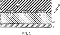
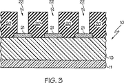
図2に示すように、構造10の上側に絶縁層20が設けられる。絶縁層20は、例えば、テトラエチルオルトシリケート(TEOS)やボロホスホシリケート・ガラス(BPSG)、ボロシリケート・ガラス(BPG)のような絶縁材料、又は他の非導電性の(ドープされ又はドープされない)酸化物、窒化物及びオキシニトライドであることが好ましい。複数の層で形成される絶縁層20は厚さが5000〜20000オングストローム前後であることが好ましい。図3に示すように、構造10の最も上側の部分に設けられる導電性の区域と相互接続部が電気的に接続される位置に、少なくとも若干の開口22が設けられる。
As shown in FIG. 2, an insulating
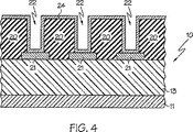
再び図3を参照すると、相互接続トレンチ22のような複数の開口が絶縁層20にパターニングされてエッチングされる。開口22は導電性区域21の部分を露出するように整列される。図4に示すように、絶縁層20を均一に覆い且つ相互接続トレンチ22の内側を覆うように、オプションの接着層24が構造10の表面の上側に堆積される。当該分野で慣用されているように、オプションの接着層24は、導電性区域21とその後に堆積される導電材料との間の接着を強化するために用いられる。デバイスの製造に用いられる材料に依存して、接着層24が不要な例も存在し得る。
Referring again to FIG. 3, a plurality of openings, such as
オプションの接着層24はチタン(Ti)のような耐熱性の金属で形成されることが好ましい。図4に示すように、1つの実施の形態においては、物理的気相成長(PVD)、化学蒸着(CVD)又は原子層堆積(ALD)を用いて、オプションの薄いTi層24が堆積される。しかし、接着層として、任意の他の適宜の材料、例えば、窒化タングステン、タングステン・タンタル、タンタル窒化ケイ素、その他の三元化合物を用いてもよい。オプションの接着層24は厚さが100〜500オングストローム前後であることが好ましく、200オングストローム前後であることが更に好ましい。
The
図5を参照すると、好ましくはタングステンを含む導電性相互接続材料が構造10の上側に且つ相互接続トレンチ22に形成される。導電性相互接続部30は、CVDやALD等を含む当該分野で慣用されている任意の技術を用いて形成される。両技術はトレンチ22の適合充填を生じる。しかし、トレンチのアスペクト比及び深さに依存して、こうした適合蒸着技術はタングステン・プラグ内にキーホールを形成する結果となり得る。典型的には、相互接続部30は1000〜5000オングストローム前後の厚さ、好ましくは2000オングストローム前後の厚さを有する。図6を参照すると、導電性相互接続部30から過剰な材料が除去される。典型的には、こうした材料は、当該分野において周知の化学機械平坦化(CMP)技術を用いて除去される。過剰な材料の除去は絶縁層20の上面25と実質的に同じ高さで停止されることが望ましい。
Referring to FIG. 5, a conductive interconnect material, preferably comprising tungsten, is formed on top of
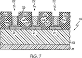
図7を参照すると、導電性相互接続部30は絶縁層20の上面25よりも適宜の距離だけ低く、凹み又は陥凹部を作るように、更に平坦化又は過剰研磨される。相互接続材料を凹ますのに、任意の適宜の方法を用いることができる。例えば、導電性相互接続部30は選択的に過剰研磨され、化学機械的に平坦化され、ウェット・エッチングされ又はドライ・エッチングされてトレンチ22内に且つ絶縁層20の面よりも低く、相互接続材料を凹ますことができる。典型的には、200〜500オングストローム前後の凹みが好ましい。
Referring to FIG. 7, the
1つの実施の形態においては、オプションとして、相互接続材料30の凹みの表面は、以後の金属メッキに対して選択的になるよう活性化される。しかし、実施の形態によっては、当業者は認識するように、面の活性化は不要である。面の活性化は多くの技術を用いて達成され得る。面は、無電解メッキの分野で公知の任意の活性化溶液、例えば塩化パラジウム溶液に対する露出によって活性化されることが好ましい。面露出のための典型的な時間枠は、選択された特定の活性化溶液に依存して、10秒前後〜2分前後である。
In one embodiment, optionally, the recessed surface of the
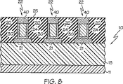
図8を参照すると、次いで、無電解メッキ・プロセスを用いて、金属が凹み内に選択的に堆積される。凹みに形成される金属層は、半導体構造における隣接の材料に適合する任意の材料を含み得る。金属層はコバルト、銀、金、銅、ニッケル、パラジウム、白金、又はそれらの合金を含むことが好ましい。金属はコバルトを含むことが最も好ましい。これは、コバルトは入手が容易であり、以後の処理のための平滑な表面を促進する微細なグレイン構造を提供するからである。 Referring to FIG. 8, metal is then selectively deposited in the recess using an electroless plating process. The metal layer formed in the recess may comprise any material that is compatible with the adjacent material in the semiconductor structure. The metal layer preferably includes cobalt, silver, gold, copper, nickel, palladium, platinum, or an alloy thereof. Most preferably, the metal comprises cobalt. This is because cobalt is readily available and provides a fine grain structure that promotes a smooth surface for subsequent processing.
200〜500オングストローム前後の厚さを持つ金属キャップを形成することが好ましい。キャップのメッキ速度を制御することにより、絶縁層20の上面と実質的に同一平面のキャップを作ることができる。基板上に過剰な金属がメッキされた場合には、過剰部分を慣用の処理方法、例えば、図8に示す構造の平坦化によって除去して金属層を分離し、図示のように個々の金属キャップ40が作られる。図8の構造は、次いで、機能回路を作るように更に処理される。
It is preferable to form a metal cap having a thickness of about 200 to 500 angstroms. By controlling the plating rate of the cap, a cap that is substantially flush with the upper surface of the insulating
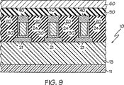
図9に示すように、適宜のカルコゲニド材料50のスタックを絶縁層20及び金属キャップ40の上側に堆積させることによって、メモリ・デバイスが形成される。カルコゲニド材料はGe3Se7Ge4Se6のようなカルコゲン化ガラスから形成し得る。このガラスは、ガラス内の銀のような拡散された金属イオンに対する導電経路を印加電圧の存在下で形成することができる。カルコゲニド・スタック50の上側に別の導電性電極60が堆積され、メモリ・デバイスの形成が完了する。不揮発性メモリ・デバイスの例は、ムーア及びギルトンに対する米国特許第6348365号に示されている。「スタック」は、拡散金属イオンを含み且つメモリ・セルを形成するに足る1つ以上の層のカルコゲニド・ガラス材料を意味する。
As shown in FIG. 9, a memory device is formed by depositing a suitable stack of
図10を参照すると、集積回路448を含む典型的なカルコゲニド型メモリ・システム400が図示されている。集積回路448は、本発明の1つ以上の実施の形態に従って製造された導電性相互接続部及びカルコゲニド型メモリを採用している。コンピュータ・システムのようなプロセッサ・システムは、一般に、マイクロプロセッサ、ディジタル信号プロセッサ、その他のプログラム可能なディジタル論理デバイスのような中央処理ユニット(CPU)444を備え、CPU444はバス452を介して入力/出力(I/O)デバイス446を通信する。集積回路448におけるカルコゲニド型メモリはバス452を介して、典型的にはメモリ・コントローラによりシステムと通信する。
Referring to FIG. 10, a typical
コンピュータ・システムの場合、システムは、バス452を介してCPU444と通信するフロッピー・ディスク454、コンパクト・ディスク(CD)ROMドライブ456等の周辺装置を備え得る。集積回路448は1つ以上の導電性相互接続部及びカルコゲニド型メモリ・デバイスを備えることができる。所望であれば、集積回路448は単一の集積回路においてCPU444等のプロセッサと組み合わされ得る。カルコゲニド型メモリ・デバイスを含む装置及びシステムの他の例は、時計、テレビジョン、携帯電話機、車両、航空機等を含む。
In the case of a computer system, the system may include peripheral devices such as a
当業者には明らかなとおり、発明の範囲から逸脱することなく、種々の変更を行うことができ、本発明は、明細書及び図面において説明した特定の実施の形態に限定されると考えられるべきではなく、特許請求の範囲の範囲よってのみ限定される。 It will be apparent to those skilled in the art that various modifications can be made without departing from the scope of the invention, and the invention should be considered limited to the specific embodiments described in the specification and drawings. Rather, it is limited only by the scope of the claims.
Claims (16)
基板の上側に第1導電性材料の層を形成する工程と、
前記基板及び前記第1導電性材料の上側に絶縁層を堆積させる工程と、
前記絶縁層に開口を形成して、前記第1導電性材料の少なくとも一部分を露出させる工程と、
前記絶縁層の上側に且つ前記開口内に第2導電性材料を堆積させる工程と、
前記第2導電性材料の一部分を除去して前記開口内に導電性区域を形成する工程と、
前記開口内の前記導電性区域を前記絶縁層の上面よりも低い高さまで凹ます工程と、
前記開口内の凹まされた前記導電性区域の上側に第3導電性材料のキャップを堆積させる工程と、
前記キャップの上側にカルコゲニド型メモリ・セル材料のスタックを堆積させる工程と、
前記カルコゲニド型メモリ・セル材料のスタックの上側に導電性材料を堆積させる工程と、
を備え、前記第3導電性材料が、コバルト、銀、金、銅、ニッケル、パラジウム、白金、及びそれらの合金の群の中から選択される方法。A method of forming a metal cap on top of a conductive interconnect in a chalcogenide type memory device, comprising:
Forming a layer of a first conductive material on the upper side of the substrate;
Depositing an insulating layer on top of the substrate and the first conductive material;
Forming an opening in the insulating layer to expose at least a portion of the first conductive material;
Depositing a second conductive material over the insulating layer and in the opening;
Removing a portion of the second conductive material to form a conductive area in the opening;
Recessed the conductive area in the opening to a height lower than the top surface of the insulating layer;
Depositing a cap of a third conductive material overlying the recessed conductive area in the opening;
Depositing a stack of chalcogenide type memory cell material on top of the cap;
Depositing a conductive material over the stack of chalcogenide-type memory cell materials;
And the third conductive material is selected from the group of cobalt, silver, gold, copper, nickel, palladium, platinum, and alloys thereof.
半導体基板上の第1導電性材料の層と、
前記第1導電性材料の層上の及び前記半導体基板上の絶縁層であって、前記第1導電性材料の層の少なくとも一部分を露出させる開口を有する絶縁層と、
前記開口内の凹んだタングステン層と、
前記タングステン層上に無電解メッキされた金属キャップであって、コバルト、銀、金、銅、ニッケル、パラジウム、白金及びそれらの合金からなる群から選択される金属を含む金属キャップと、
前記金属キャップ上のカルコゲニド型メモリ・セルのスタックと、
前記スタック上の導電性材料と、
を具備する導電性相互接続部。A conductive interconnect for a chalcogenide-type memory device, comprising:
A layer of a first conductive material on a semiconductor substrate;
An insulating layer on the layer of the first conductive material and on the semiconductor substrate, the insulating layer having an opening exposing at least a portion of the layer of the first conductive material;
A recessed tungsten layer in the opening;
A metal cap electrolessly plated on the tungsten layer, the metal cap including a metal selected from the group consisting of cobalt, silver, gold, copper, nickel, palladium, platinum, and alloys thereof;
A stack of chalcogenide memory cells on the metal cap;
A conductive material on the stack;
A conductive interconnect comprising:
前記プロセッサに結合され、且つ請求項10〜12のうちのいずれか1つに記載の導電性相互接続部を備えるカルコゲニド型メモリ・デバイスと
を備えるプロセッサ型システム。A processor;
A processor-type system comprising: a chalcogenide-type memory device coupled to the processor and comprising a conductive interconnect according to any one of claims 10-12.
基板上に第1導電性材料の層を形成する工程と、
前記第1導電性材料の層及び前記基板の上側に絶縁層を堆積させる工程と、
前記絶縁層に開口を形成して、前記第1導電性材料の少なくとも一部分を露出させる工程と、
前記絶縁層の上側に且つ前記開口内に第2導電性材料を堆積させる工程と、
前記第2導電性材料の一部分を除去して、前記開口内に導電性区域を形成する工程と、
前記開口内の前記導電性区域を前記絶縁層の上面よりも低い高さまで凹ます工程と、
前記開口内の凹まされた前記導電性区域の上側に、無電解メッキによって第3導電性材料のキャップを形成する工程と、
前記キャップの上側にカルコゲニド型メモリ・セル材料のスタックを堆積させる工程と、
前記カルコゲニド型メモリ・セル材料のスタックの上側に第4導電性材料を堆積させる工程と
を具備する方法。A method of forming a metal cap on a conductive interconnect in a chalcogenide type memory device, comprising:
Forming a layer of a first conductive material on a substrate;
Depositing an insulating layer overlying the first conductive material layer and the substrate;
Forming an opening in the insulating layer to expose at least a portion of the first conductive material;
Depositing a second conductive material over the insulating layer and in the opening;
Removing a portion of the second conductive material to form a conductive area in the opening;
Recessed the conductive area in the opening to a height lower than the top surface of the insulating layer;
Forming a cap of a third conductive material by electroless plating over the recessed conductive area in the opening;
Depositing a stack of chalcogenide type memory cell material on top of the cap;
Depositing a fourth conductive material on top of the chalcogenide memory cell material stack.
半導体デバイスが形成された半導体構造を設ける工程と、
前記半導体構造の上側に絶縁層を形成する工程と、
前記半導体構造に至るトレンチを前記絶縁層に形成する工程と、
前記半導体デバイスの少なくとも一部分を露出させる工程と、
タングステンを含む導電性材料で前記トレンチを充填する工程と、
前記導電性材料を前記絶縁層の上面よりも低い高さまで凹ます工程と、
凹まされた前記導電性材料の上側に、コバルト、銀、金、銅、ニッケル、パラジウム、白金及びそれらの合金からなる群から選択される金属を含む金属キャップを無電解メッキする工程と、
前記キャップの上側にカルコゲニド型メモリ・セル材料のスタックを堆積させる工程と、
前記カルコゲニド型メモリ・セル材料のスタックの上側に導電性材料を堆積させる工程と、
を具備する方法。A method of forming a conductive interconnect for a semiconductor circuit comprising:
Providing a semiconductor structure having a semiconductor device formed thereon;
Forming an insulating layer above the semiconductor structure;
Forming a trench in the insulating layer leading to the semiconductor structure;
Exposing at least a portion of the semiconductor device;
Filling the trench with a conductive material comprising tungsten;
Denting the conductive material to a height lower than the top surface of the insulating layer;
Electrolessly plating a metal cap containing a metal selected from the group consisting of cobalt, silver, gold, copper, nickel, palladium, platinum, and alloys thereof on the recessed conductive material;
Depositing a stack of chalcogenide type memory cell material on top of the cap;
Depositing a conductive material over the stack of chalcogenide-type memory cell materials;
A method comprising:
Applications Claiming Priority (3)
| Application Number | Priority Date | Filing Date | Title |
|---|---|---|---|
| US10/980,658 | 2004-11-03 | ||
| US10/980,658 US7189626B2 (en) | 2004-11-03 | 2004-11-03 | Electroless plating of metal caps for chalcogenide-based memory devices |
| PCT/US2005/037310 WO2006052394A1 (en) | 2004-11-03 | 2005-10-18 | Electroless plating of metal caps for chalcogenide-based memory devices |
Publications (2)
| Publication Number | Publication Date |
|---|---|
| JP2008519465A JP2008519465A (en) | 2008-06-05 |
| JP5154942B2 true JP5154942B2 (en) | 2013-02-27 |
Family
ID=35695541
Family Applications (1)
| Application Number | Title | Priority Date | Filing Date |
|---|---|---|---|
| JP2007540323A Expired - Lifetime JP5154942B2 (en) | 2004-11-03 | 2005-10-18 | Electroless plating of metal caps for chalcogenide-type memory devices |
Country Status (7)
| Country | Link |
|---|---|
| US (2) | US7189626B2 (en) |
| EP (1) | EP1812977B1 (en) |
| JP (1) | JP5154942B2 (en) |
| KR (1) | KR101208757B1 (en) |
| CN (1) | CN101080825B (en) |
| TW (1) | TWI286818B (en) |
| WO (1) | WO2006052394A1 (en) |
Families Citing this family (427)
| Publication number | Priority date | Publication date | Assignee | Title |
|---|---|---|---|---|
| US7959577B2 (en) * | 2007-09-06 | 2011-06-14 | Baxano, Inc. | Method, system, and apparatus for neural localization |
| US7812404B2 (en) * | 2005-05-09 | 2010-10-12 | Sandisk 3D Llc | Nonvolatile memory cell comprising a diode and a resistance-switching material |
| US7407885B2 (en) * | 2005-05-11 | 2008-08-05 | Micron Technology, Inc. | Methods of forming electrically conductive plugs |
| US7686874B2 (en) * | 2005-06-28 | 2010-03-30 | Micron Technology, Inc. | Electroless plating bath composition and method of use |
| US7348238B2 (en) * | 2005-08-22 | 2008-03-25 | Micron Technology, Inc. | Bottom electrode for memory device and method of forming the same |
| US7834338B2 (en) | 2005-11-23 | 2010-11-16 | Sandisk 3D Llc | Memory cell comprising nickel-cobalt oxide switching element |
| US7875871B2 (en) * | 2006-03-31 | 2011-01-25 | Sandisk 3D Llc | Heterojunction device comprising a semiconductor and a resistivity-switching oxide or nitride |
| US7808810B2 (en) * | 2006-03-31 | 2010-10-05 | Sandisk 3D Llc | Multilevel nonvolatile memory cell comprising a resistivity-switching oxide or nitride and an antifuse |
| US7829875B2 (en) * | 2006-03-31 | 2010-11-09 | Sandisk 3D Llc | Nonvolatile rewritable memory cell comprising a resistivity-switching oxide or nitride and an antifuse |
| KR100780865B1 (en) * | 2006-07-19 | 2007-11-30 | 삼성전자주식회사 | Method of Forming Semiconductor Device Including Phase Change Film |
| JP4740071B2 (en) * | 2006-08-31 | 2011-08-03 | 株式会社東芝 | Semiconductor device |
| KR100852206B1 (en) * | 2007-04-04 | 2008-08-13 | 삼성전자주식회사 | Resistive memory device and manufacturing method thereof. |
| KR100881055B1 (en) * | 2007-06-20 | 2009-01-30 | 삼성전자주식회사 | Phase change memory unit, manufacturing method thereof, phase change memory device including same and manufacturing method thereof |
| US7902537B2 (en) * | 2007-06-29 | 2011-03-08 | Sandisk 3D Llc | Memory cell that employs a selectively grown reversible resistance-switching element and methods of forming the same |
| US7846785B2 (en) * | 2007-06-29 | 2010-12-07 | Sandisk 3D Llc | Memory cell that employs a selectively deposited reversible resistance-switching element and methods of forming the same |
| US7824956B2 (en) * | 2007-06-29 | 2010-11-02 | Sandisk 3D Llc | Memory cell that employs a selectively grown reversible resistance-switching element and methods of forming the same |
| EP2485258B1 (en) * | 2007-06-29 | 2014-03-26 | Sandisk 3D LLC | Method of forming a memory cell that employs a selectively deposited reversible resistance-switching element |
| US8233308B2 (en) | 2007-06-29 | 2012-07-31 | Sandisk 3D Llc | Memory cell that employs a selectively deposited reversible resistance-switching element and methods of forming the same |
| US20090072348A1 (en) * | 2007-09-19 | 2009-03-19 | Ulrich Klostermann | Integrated Circuits; Methods for Manufacturing an Integrated Circuit and Memory Module |
| US7768812B2 (en) | 2008-01-15 | 2010-08-03 | Micron Technology, Inc. | Memory cells, memory cell programming methods, memory cell reading methods, memory cell operating methods, and memory devices |
| US8034655B2 (en) | 2008-04-08 | 2011-10-11 | Micron Technology, Inc. | Non-volatile resistive oxide memory cells, non-volatile resistive oxide memory arrays, and methods of forming non-volatile resistive oxide memory cells and memory arrays |
| US8211743B2 (en) | 2008-05-02 | 2012-07-03 | Micron Technology, Inc. | Methods of forming non-volatile memory cells having multi-resistive state material between conductive electrodes |
| US8134137B2 (en) | 2008-06-18 | 2012-03-13 | Micron Technology, Inc. | Memory device constructions, memory cell forming methods, and semiconductor construction forming methods |
| US9343665B2 (en) | 2008-07-02 | 2016-05-17 | Micron Technology, Inc. | Methods of forming a non-volatile resistive oxide memory cell and methods of forming a non-volatile resistive oxide memory array |
| US8455298B2 (en) * | 2008-08-18 | 2013-06-04 | Contour Semiconductor, Inc. | Method for forming self-aligned phase-change semiconductor diode memory |
| US9394608B2 (en) | 2009-04-06 | 2016-07-19 | Asm America, Inc. | Semiconductor processing reactor and components thereof |
| US8802201B2 (en) | 2009-08-14 | 2014-08-12 | Asm America, Inc. | Systems and methods for thin-film deposition of metal oxides using excited nitrogen-oxygen species |
| CN101996943B (en) * | 2009-08-18 | 2013-12-04 | 展晶科技(深圳)有限公司 | Method for separating material layer |
| US8686390B2 (en) * | 2009-11-30 | 2014-04-01 | Panasonic Corporation | Nonvolatile memory element having a variable resistance layer whose resistance value changes according to an applied electric signal |
| US8427859B2 (en) | 2010-04-22 | 2013-04-23 | Micron Technology, Inc. | Arrays of vertically stacked tiers of non-volatile cross point memory cells, methods of forming arrays of vertically stacked tiers of non-volatile cross point memory cells, and methods of reading a data value stored by an array of vertically stacked tiers of non-volatile cross point memory cells |
| US8411477B2 (en) | 2010-04-22 | 2013-04-02 | Micron Technology, Inc. | Arrays of vertically stacked tiers of non-volatile cross point memory cells, methods of forming arrays of vertically stacked tiers of non-volatile cross point memory cells, and methods of reading a data value stored by an array of vertically stacked tiers of non-volatile cross point memory cells |
| US8289763B2 (en) | 2010-06-07 | 2012-10-16 | Micron Technology, Inc. | Memory arrays |
| US9012307B2 (en) | 2010-07-13 | 2015-04-21 | Crossbar, Inc. | Two terminal resistive switching device structure and method of fabricating |
| US8946046B1 (en) | 2012-05-02 | 2015-02-03 | Crossbar, Inc. | Guided path for forming a conductive filament in RRAM |
| US9601692B1 (en) | 2010-07-13 | 2017-03-21 | Crossbar, Inc. | Hetero-switching layer in a RRAM device and method |
| US9570678B1 (en) | 2010-06-08 | 2017-02-14 | Crossbar, Inc. | Resistive RAM with preferental filament formation region and methods |
| US8441835B2 (en) | 2010-06-11 | 2013-05-14 | Crossbar, Inc. | Interface control for improved switching in RRAM |
| JP5981424B2 (en) * | 2010-06-11 | 2016-08-31 | クロスバー, インコーポレイテッドCrossbar, Inc. | Columnar structure and method for memory device |
| US8374018B2 (en) | 2010-07-09 | 2013-02-12 | Crossbar, Inc. | Resistive memory using SiGe material |
| US8884261B2 (en) | 2010-08-23 | 2014-11-11 | Crossbar, Inc. | Device switching using layered device structure |
| US8569172B1 (en) | 2012-08-14 | 2013-10-29 | Crossbar, Inc. | Noble metal/non-noble metal electrode for RRAM applications |
| US8467227B1 (en) | 2010-11-04 | 2013-06-18 | Crossbar, Inc. | Hetero resistive switching material layer in RRAM device and method |
| US8168506B2 (en) | 2010-07-13 | 2012-05-01 | Crossbar, Inc. | On/off ratio for non-volatile memory device and method |
| US8947908B2 (en) | 2010-11-04 | 2015-02-03 | Crossbar, Inc. | Hetero-switching layer in a RRAM device and method |
| US9401475B1 (en) | 2010-08-23 | 2016-07-26 | Crossbar, Inc. | Method for silver deposition for a non-volatile memory device |
| US8404553B2 (en) | 2010-08-23 | 2013-03-26 | Crossbar, Inc. | Disturb-resistant non-volatile memory device and method |
| US8492195B2 (en) | 2010-08-23 | 2013-07-23 | Crossbar, Inc. | Method for forming stackable non-volatile resistive switching memory devices |
| US8889521B1 (en) | 2012-09-14 | 2014-11-18 | Crossbar, Inc. | Method for silver deposition for a non-volatile memory device |
| US8841196B1 (en) | 2010-09-29 | 2014-09-23 | Crossbar, Inc. | Selective deposition of silver for non-volatile memory device fabrication |
| US8558212B2 (en) | 2010-09-29 | 2013-10-15 | Crossbar, Inc. | Conductive path in switching material in a resistive random access memory device and control |
| US8391049B2 (en) | 2010-09-29 | 2013-03-05 | Crossbar, Inc. | Resistor structure for a non-volatile memory device and method |
| US8351242B2 (en) | 2010-09-29 | 2013-01-08 | Micron Technology, Inc. | Electronic devices, memory devices and memory arrays |
| US8759809B2 (en) | 2010-10-21 | 2014-06-24 | Micron Technology, Inc. | Integrated circuitry comprising nonvolatile memory cells having platelike electrode and ion conductive material layer |
| US8187945B2 (en) | 2010-10-27 | 2012-05-29 | Crossbar, Inc. | Method for obtaining smooth, continuous silver film |
| US8796661B2 (en) | 2010-11-01 | 2014-08-05 | Micron Technology, Inc. | Nonvolatile memory cells and methods of forming nonvolatile memory cell |
| US8526213B2 (en) | 2010-11-01 | 2013-09-03 | Micron Technology, Inc. | Memory cells, methods of programming memory cells, and methods of forming memory cells |
| US8502185B2 (en) | 2011-05-31 | 2013-08-06 | Crossbar, Inc. | Switching device having a non-linear element |
| US8258020B2 (en) | 2010-11-04 | 2012-09-04 | Crossbar Inc. | Interconnects for stacked non-volatile memory device and method |
| USRE46335E1 (en) | 2010-11-04 | 2017-03-07 | Crossbar, Inc. | Switching device having a non-linear element |
| US8088688B1 (en) | 2010-11-05 | 2012-01-03 | Crossbar, Inc. | p+ polysilicon material on aluminum for non-volatile memory device and method |
| US9454997B2 (en) | 2010-12-02 | 2016-09-27 | Micron Technology, Inc. | Array of nonvolatile memory cells having at least five memory cells per unit cell, having a plurality of the unit cells which individually comprise three elevational regions of programmable material, and/or having a continuous volume having a combination of a plurality of vertically oriented memory cells and a plurality of horizontally oriented memory cells; array of vertically stacked tiers of nonvolatile memory cells |
| US8431458B2 (en) | 2010-12-27 | 2013-04-30 | Micron Technology, Inc. | Methods of forming a nonvolatile memory cell and methods of forming an array of nonvolatile memory cells |
| US8930174B2 (en) | 2010-12-28 | 2015-01-06 | Crossbar, Inc. | Modeling technique for resistive random access memory (RRAM) cells |
| US8815696B1 (en) | 2010-12-31 | 2014-08-26 | Crossbar, Inc. | Disturb-resistant non-volatile memory device using via-fill and etchback technique |
| US9153623B1 (en) | 2010-12-31 | 2015-10-06 | Crossbar, Inc. | Thin film transistor steering element for a non-volatile memory device |
| US8791010B1 (en) | 2010-12-31 | 2014-07-29 | Crossbar, Inc. | Silver interconnects for stacked non-volatile memory device and method |
| US8791447B2 (en) | 2011-01-20 | 2014-07-29 | Micron Technology, Inc. | Arrays of nonvolatile memory cells and methods of forming arrays of nonvolatile memory cells |
| US8488365B2 (en) | 2011-02-24 | 2013-07-16 | Micron Technology, Inc. | Memory cells |
| US8524599B2 (en) | 2011-03-17 | 2013-09-03 | Micron Technology, Inc. | Methods of forming at least one conductive element and methods of forming a semiconductor structure |
| US8537592B2 (en) | 2011-04-15 | 2013-09-17 | Micron Technology, Inc. | Arrays of nonvolatile memory cells and methods of forming arrays of nonvolatile memory cells |
| US8450710B2 (en) | 2011-05-27 | 2013-05-28 | Crossbar, Inc. | Low temperature p+ silicon junction material for a non-volatile memory device |
| US9620206B2 (en) | 2011-05-31 | 2017-04-11 | Crossbar, Inc. | Memory array architecture with two-terminal memory cells |
| US8394670B2 (en) | 2011-05-31 | 2013-03-12 | Crossbar, Inc. | Vertical diodes for non-volatile memory device |
| US20120309188A1 (en) * | 2011-05-31 | 2012-12-06 | Crossbar, Inc. | Method to improve adhesion for a silver filled oxide via for a non-volatile memory device |
| US8619459B1 (en) | 2011-06-23 | 2013-12-31 | Crossbar, Inc. | High operating speed resistive random access memory |
| US9627443B2 (en) | 2011-06-30 | 2017-04-18 | Crossbar, Inc. | Three-dimensional oblique two-terminal memory with enhanced electric field |
| US9564587B1 (en) | 2011-06-30 | 2017-02-07 | Crossbar, Inc. | Three-dimensional two-terminal memory with enhanced electric field and segmented interconnects |
| US8659929B2 (en) | 2011-06-30 | 2014-02-25 | Crossbar, Inc. | Amorphous silicon RRAM with non-linear device and operation |
| US9166163B2 (en) | 2011-06-30 | 2015-10-20 | Crossbar, Inc. | Sub-oxide interface layer for two-terminal memory |
| US8946669B1 (en) | 2012-04-05 | 2015-02-03 | Crossbar, Inc. | Resistive memory device and fabrication methods |
| US20130023129A1 (en) | 2011-07-20 | 2013-01-24 | Asm America, Inc. | Pressure transmitter for a semiconductor processing environment |
| WO2013015776A1 (en) | 2011-07-22 | 2013-01-31 | Crossbar, Inc. | Seed layer for a p + silicon germanium material for a non-volatile memory device and method |
| US8674724B2 (en) | 2011-07-29 | 2014-03-18 | Crossbar, Inc. | Field programmable gate array utilizing two-terminal non-volatile memory |
| US10056907B1 (en) | 2011-07-29 | 2018-08-21 | Crossbar, Inc. | Field programmable gate array utilizing two-terminal non-volatile memory |
| US9729155B2 (en) | 2011-07-29 | 2017-08-08 | Crossbar, Inc. | Field programmable gate array utilizing two-terminal non-volatile memory |
| CN102437099A (en) * | 2011-09-08 | 2012-05-02 | 上海华力微电子有限公司 | Forming method of contact hole structure for reducing resistance of contact hole |
| CN102437098A (en) * | 2011-09-08 | 2012-05-02 | 上海华力微电子有限公司 | Forming method of contact hole for reducing contact resistance |
| CN102437097A (en) * | 2011-09-08 | 2012-05-02 | 上海华力微电子有限公司 | Novel manufacturing method of contact hole |
| US9017481B1 (en) | 2011-10-28 | 2015-04-28 | Asm America, Inc. | Process feed management for semiconductor substrate processing |
| US8716098B1 (en) | 2012-03-09 | 2014-05-06 | Crossbar, Inc. | Selective removal method and structure of silver in resistive switching device for a non-volatile memory device |
| US9087576B1 (en) | 2012-03-29 | 2015-07-21 | Crossbar, Inc. | Low temperature fabrication method for a three-dimensional memory device and structure |
| US8946667B1 (en) | 2012-04-13 | 2015-02-03 | Crossbar, Inc. | Barrier structure for a silver based RRAM and method |
| US9685608B2 (en) | 2012-04-13 | 2017-06-20 | Crossbar, Inc. | Reduced diffusion in metal electrode for two-terminal memory |
| US8658476B1 (en) | 2012-04-20 | 2014-02-25 | Crossbar, Inc. | Low temperature P+ polycrystalline silicon material for non-volatile memory device |
| US8796658B1 (en) | 2012-05-07 | 2014-08-05 | Crossbar, Inc. | Filamentary based non-volatile resistive memory device and method |
| US8765566B2 (en) | 2012-05-10 | 2014-07-01 | Crossbar, Inc. | Line and space architecture for a non-volatile memory device |
| US9070859B1 (en) | 2012-05-25 | 2015-06-30 | Crossbar, Inc. | Low temperature deposition method for polycrystalline silicon material for a non-volatile memory device |
| US9741765B1 (en) | 2012-08-14 | 2017-08-22 | Crossbar, Inc. | Monolithically integrated resistive memory using integrated-circuit foundry compatible processes |
| US9583701B1 (en) | 2012-08-14 | 2017-02-28 | Crossbar, Inc. | Methods for fabricating resistive memory device switching material using ion implantation |
| US8946673B1 (en) | 2012-08-24 | 2015-02-03 | Crossbar, Inc. | Resistive switching device structure with improved data retention for non-volatile memory device and method |
| US8796102B1 (en) | 2012-08-29 | 2014-08-05 | Crossbar, Inc. | Device structure for a RRAM and method |
| US9312483B2 (en) | 2012-09-24 | 2016-04-12 | Crossbar, Inc. | Electrode structure for a non-volatile memory device and method |
| US9576616B2 (en) | 2012-10-10 | 2017-02-21 | Crossbar, Inc. | Non-volatile memory with overwrite capability and low write amplification |
| US10714315B2 (en) | 2012-10-12 | 2020-07-14 | Asm Ip Holdings B.V. | Semiconductor reaction chamber showerhead |
| US11068620B2 (en) | 2012-11-09 | 2021-07-20 | Crossbar, Inc. | Secure circuit integrated with memory layer |
| US8982647B2 (en) | 2012-11-14 | 2015-03-17 | Crossbar, Inc. | Resistive random access memory equalization and sensing |
| US9412790B1 (en) | 2012-12-04 | 2016-08-09 | Crossbar, Inc. | Scalable RRAM device architecture for a non-volatile memory device and method |
| US9406379B2 (en) | 2013-01-03 | 2016-08-02 | Crossbar, Inc. | Resistive random access memory with non-linear current-voltage relationship |
| US9112145B1 (en) | 2013-01-31 | 2015-08-18 | Crossbar, Inc. | Rectified switching of two-terminal memory via real time filament formation |
| US9324942B1 (en) | 2013-01-31 | 2016-04-26 | Crossbar, Inc. | Resistive memory cell with solid state diode |
| US20160376700A1 (en) | 2013-02-01 | 2016-12-29 | Asm Ip Holding B.V. | System for treatment of deposition reactor |
| US8934280B1 (en) | 2013-02-06 | 2015-01-13 | Crossbar, Inc. | Capacitive discharge programming for two-terminal memory cells |
| US10290801B2 (en) | 2014-02-07 | 2019-05-14 | Crossbar, Inc. | Scalable silicon based resistive memory device |
| US11015245B2 (en) | 2014-03-19 | 2021-05-25 | Asm Ip Holding B.V. | Gas-phase reactor and system having exhaust plenum and components thereof |
| US9577192B2 (en) * | 2014-05-21 | 2017-02-21 | Sony Semiconductor Solutions Corporation | Method for forming a metal cap in a semiconductor memory device |
| US10858737B2 (en) | 2014-07-28 | 2020-12-08 | Asm Ip Holding B.V. | Showerhead assembly and components thereof |
| US9603247B2 (en) | 2014-08-11 | 2017-03-21 | Intel Corporation | Electronic package with narrow-factor via including finish layer |
| US9890456B2 (en) | 2014-08-21 | 2018-02-13 | Asm Ip Holding B.V. | Method and system for in situ formation of gas-phase compounds |
| US10941490B2 (en) | 2014-10-07 | 2021-03-09 | Asm Ip Holding B.V. | Multiple temperature range susceptor, assembly, reactor and system including the susceptor, and methods of using the same |
| US10276355B2 (en) | 2015-03-12 | 2019-04-30 | Asm Ip Holding B.V. | Multi-zone reactor, system including the reactor, and method of using the same |
| US10458018B2 (en) | 2015-06-26 | 2019-10-29 | Asm Ip Holding B.V. | Structures including metal carbide material, devices including the structures, and methods of forming same |
| US10211308B2 (en) | 2015-10-21 | 2019-02-19 | Asm Ip Holding B.V. | NbMC layers |
| US11139308B2 (en) | 2015-12-29 | 2021-10-05 | Asm Ip Holding B.V. | Atomic layer deposition of III-V compounds to form V-NAND devices |
| US10529554B2 (en) | 2016-02-19 | 2020-01-07 | Asm Ip Holding B.V. | Method for forming silicon nitride film selectively on sidewalls or flat surfaces of trenches |
| US10343920B2 (en) | 2016-03-18 | 2019-07-09 | Asm Ip Holding B.V. | Aligned carbon nanotubes |
| US10190213B2 (en) | 2016-04-21 | 2019-01-29 | Asm Ip Holding B.V. | Deposition of metal borides |
| US10865475B2 (en) | 2016-04-21 | 2020-12-15 | Asm Ip Holding B.V. | Deposition of metal borides and silicides |
| US10367080B2 (en) | 2016-05-02 | 2019-07-30 | Asm Ip Holding B.V. | Method of forming a germanium oxynitride film |
| US11453943B2 (en) | 2016-05-25 | 2022-09-27 | Asm Ip Holding B.V. | Method for forming carbon-containing silicon/metal oxide or nitride film by ALD using silicon precursor and hydrocarbon precursor |
| US9859151B1 (en) | 2016-07-08 | 2018-01-02 | Asm Ip Holding B.V. | Selective film deposition method to form air gaps |
| US10612137B2 (en) | 2016-07-08 | 2020-04-07 | Asm Ip Holdings B.V. | Organic reactants for atomic layer deposition |
| US10714385B2 (en) | 2016-07-19 | 2020-07-14 | Asm Ip Holding B.V. | Selective deposition of tungsten |
| US9887082B1 (en) | 2016-07-28 | 2018-02-06 | Asm Ip Holding B.V. | Method and apparatus for filling a gap |
| KR102532607B1 (en) | 2016-07-28 | 2023-05-15 | 에이에스엠 아이피 홀딩 비.브이. | Substrate processing apparatus and method of operating the same |
| US9812320B1 (en) | 2016-07-28 | 2017-11-07 | Asm Ip Holding B.V. | Method and apparatus for filling a gap |
| US9852990B1 (en) | 2016-08-17 | 2017-12-26 | International Business Machines Corporation | Cobalt first layer advanced metallization for interconnects |
| US10115670B2 (en) | 2016-08-17 | 2018-10-30 | International Business Machines Corporation | Formation of advanced interconnects including set of metal conductor structures in patterned dielectric layer |
| US9716063B1 (en) | 2016-08-17 | 2017-07-25 | International Business Machines Corporation | Cobalt top layer advanced metallization for interconnects |
| US9941212B2 (en) | 2016-08-17 | 2018-04-10 | International Business Machines Corporation | Nitridized ruthenium layer for formation of cobalt interconnects |
| US9859215B1 (en) | 2016-08-17 | 2018-01-02 | International Business Machines Corporation | Formation of advanced interconnects |
| US10643826B2 (en) | 2016-10-26 | 2020-05-05 | Asm Ip Holdings B.V. | Methods for thermally calibrating reaction chambers |
| US11532757B2 (en) | 2016-10-27 | 2022-12-20 | Asm Ip Holding B.V. | Deposition of charge trapping layers |
| US10229833B2 (en) | 2016-11-01 | 2019-03-12 | Asm Ip Holding B.V. | Methods for forming a transition metal nitride film on a substrate by atomic layer deposition and related semiconductor device structures |
| US10714350B2 (en) | 2016-11-01 | 2020-07-14 | ASM IP Holdings, B.V. | Methods for forming a transition metal niobium nitride film on a substrate by atomic layer deposition and related semiconductor device structures |
| KR102546317B1 (en) | 2016-11-15 | 2023-06-21 | 에이에스엠 아이피 홀딩 비.브이. | Gas supply unit and substrate processing apparatus including the same |
| KR102762543B1 (en) | 2016-12-14 | 2025-02-05 | 에이에스엠 아이피 홀딩 비.브이. | Substrate processing apparatus |
| US11581186B2 (en) | 2016-12-15 | 2023-02-14 | Asm Ip Holding B.V. | Sequential infiltration synthesis apparatus |
| US11447861B2 (en) | 2016-12-15 | 2022-09-20 | Asm Ip Holding B.V. | Sequential infiltration synthesis apparatus and a method of forming a patterned structure |
| KR102700194B1 (en) | 2016-12-19 | 2024-08-28 | 에이에스엠 아이피 홀딩 비.브이. | Substrate processing apparatus |
| US10269558B2 (en) | 2016-12-22 | 2019-04-23 | Asm Ip Holding B.V. | Method of forming a structure on a substrate |
| US10867788B2 (en) | 2016-12-28 | 2020-12-15 | Asm Ip Holding B.V. | Method of forming a structure on a substrate |
| US11390950B2 (en) | 2017-01-10 | 2022-07-19 | Asm Ip Holding B.V. | Reactor system and method to reduce residue buildup during a film deposition process |
| TWI753993B (en) * | 2017-01-20 | 2022-02-01 | 日商東京威力科創股份有限公司 | Interconnect structure and method of forming the same |
| US10468261B2 (en) | 2017-02-15 | 2019-11-05 | Asm Ip Holding B.V. | Methods for forming a metallic film on a substrate by cyclical deposition and related semiconductor device structures |
| US10529563B2 (en) | 2017-03-29 | 2020-01-07 | Asm Ip Holdings B.V. | Method for forming doped metal oxide films on a substrate by cyclical deposition and related semiconductor device structures |
| CN108695235B (en) * | 2017-04-05 | 2019-08-13 | 联华电子股份有限公司 | Method for improving tungsten metal layer etching micro-load |
| KR102457289B1 (en) | 2017-04-25 | 2022-10-21 | 에이에스엠 아이피 홀딩 비.브이. | Method for depositing a thin film and manufacturing a semiconductor device |
| US10770286B2 (en) | 2017-05-08 | 2020-09-08 | Asm Ip Holdings B.V. | Methods for selectively forming a silicon nitride film on a substrate and related semiconductor device structures |
| US10892156B2 (en) | 2017-05-08 | 2021-01-12 | Asm Ip Holding B.V. | Methods for forming a silicon nitride film on a substrate and related semiconductor device structures |
| US10886123B2 (en) | 2017-06-02 | 2021-01-05 | Asm Ip Holding B.V. | Methods for forming low temperature semiconductor layers and related semiconductor device structures |
| US12040200B2 (en) | 2017-06-20 | 2024-07-16 | Asm Ip Holding B.V. | Semiconductor processing apparatus and methods for calibrating a semiconductor processing apparatus |
| US11306395B2 (en) | 2017-06-28 | 2022-04-19 | Asm Ip Holding B.V. | Methods for depositing a transition metal nitride film on a substrate by atomic layer deposition and related deposition apparatus |
| US10685834B2 (en) | 2017-07-05 | 2020-06-16 | Asm Ip Holdings B.V. | Methods for forming a silicon germanium tin layer and related semiconductor device structures |
| KR20190009245A (en) | 2017-07-18 | 2019-01-28 | 에이에스엠 아이피 홀딩 비.브이. | Methods for forming a semiconductor device structure and related semiconductor device structures |
| US11374112B2 (en) | 2017-07-19 | 2022-06-28 | Asm Ip Holding B.V. | Method for depositing a group IV semiconductor and related semiconductor device structures |
| US11018002B2 (en) | 2017-07-19 | 2021-05-25 | Asm Ip Holding B.V. | Method for selectively depositing a Group IV semiconductor and related semiconductor device structures |
| US10541333B2 (en) | 2017-07-19 | 2020-01-21 | Asm Ip Holding B.V. | Method for depositing a group IV semiconductor and related semiconductor device structures |
| US10590535B2 (en) | 2017-07-26 | 2020-03-17 | Asm Ip Holdings B.V. | Chemical treatment, deposition and/or infiltration apparatus and method for using the same |
| TWI815813B (en) | 2017-08-04 | 2023-09-21 | 荷蘭商Asm智慧財產控股公司 | Showerhead assembly for distributing a gas within a reaction chamber |
| US10770336B2 (en) | 2017-08-08 | 2020-09-08 | Asm Ip Holding B.V. | Substrate lift mechanism and reactor including same |
| US10692741B2 (en) | 2017-08-08 | 2020-06-23 | Asm Ip Holdings B.V. | Radiation shield |
| US11139191B2 (en) | 2017-08-09 | 2021-10-05 | Asm Ip Holding B.V. | Storage apparatus for storing cassettes for substrates and processing apparatus equipped therewith |
| US11769682B2 (en) | 2017-08-09 | 2023-09-26 | Asm Ip Holding B.V. | Storage apparatus for storing cassettes for substrates and processing apparatus equipped therewith |
| US10566519B2 (en) | 2017-08-18 | 2020-02-18 | Taiwan Semiconductor Manufacturing Co., Ltd. | Method for forming a flat bottom electrode via (BEVA) top surface for memory |
| US11830730B2 (en) | 2017-08-29 | 2023-11-28 | Asm Ip Holding B.V. | Layer forming method and apparatus |
| US11056344B2 (en) | 2017-08-30 | 2021-07-06 | Asm Ip Holding B.V. | Layer forming method |
| KR102491945B1 (en) | 2017-08-30 | 2023-01-26 | 에이에스엠 아이피 홀딩 비.브이. | Substrate processing apparatus |
| US11295980B2 (en) | 2017-08-30 | 2022-04-05 | Asm Ip Holding B.V. | Methods for depositing a molybdenum metal film over a dielectric surface of a substrate by a cyclical deposition process and related semiconductor device structures |
| KR102401446B1 (en) | 2017-08-31 | 2022-05-24 | 에이에스엠 아이피 홀딩 비.브이. | Substrate processing apparatus |
| KR102630301B1 (en) | 2017-09-21 | 2024-01-29 | 에이에스엠 아이피 홀딩 비.브이. | Method of sequential infiltration synthesis treatment of infiltrateable material and structures and devices formed using same |
| US10844484B2 (en) | 2017-09-22 | 2020-11-24 | Asm Ip Holding B.V. | Apparatus for dispensing a vapor phase reactant to a reaction chamber and related methods |
| US10658205B2 (en) | 2017-09-28 | 2020-05-19 | Asm Ip Holdings B.V. | Chemical dispensing apparatus and methods for dispensing a chemical to a reaction chamber |
| US10403504B2 (en) | 2017-10-05 | 2019-09-03 | Asm Ip Holding B.V. | Method for selectively depositing a metallic film on a substrate |
| US10319588B2 (en) | 2017-10-10 | 2019-06-11 | Asm Ip Holding B.V. | Method for depositing a metal chalcogenide on a substrate by cyclical deposition |
| US10923344B2 (en) | 2017-10-30 | 2021-02-16 | Asm Ip Holding B.V. | Methods for forming a semiconductor structure and related semiconductor structures |
| US10910262B2 (en) * | 2017-11-16 | 2021-02-02 | Asm Ip Holding B.V. | Method of selectively depositing a capping layer structure on a semiconductor device structure |
| US11022879B2 (en) | 2017-11-24 | 2021-06-01 | Asm Ip Holding B.V. | Method of forming an enhanced unexposed photoresist layer |
| JP7214724B2 (en) | 2017-11-27 | 2023-01-30 | エーエスエム アイピー ホールディング ビー.ブイ. | Storage device for storing wafer cassettes used in batch furnaces |
| TWI791689B (en) | 2017-11-27 | 2023-02-11 | 荷蘭商Asm智慧財產控股私人有限公司 | Apparatus including a clean mini environment |
| US10872771B2 (en) | 2018-01-16 | 2020-12-22 | Asm Ip Holding B. V. | Method for depositing a material film on a substrate within a reaction chamber by a cyclical deposition process and related device structures |
| KR102695659B1 (en) | 2018-01-19 | 2024-08-14 | 에이에스엠 아이피 홀딩 비.브이. | Method for depositing a gap filling layer by plasma assisted deposition |
| TWI799494B (en) | 2018-01-19 | 2023-04-21 | 荷蘭商Asm 智慧財產控股公司 | Deposition method |
| US11018047B2 (en) | 2018-01-25 | 2021-05-25 | Asm Ip Holding B.V. | Hybrid lift pin |
| USD880437S1 (en) | 2018-02-01 | 2020-04-07 | Asm Ip Holding B.V. | Gas supply plate for semiconductor manufacturing apparatus |
| US11081345B2 (en) | 2018-02-06 | 2021-08-03 | Asm Ip Holding B.V. | Method of post-deposition treatment for silicon oxide film |
| US11685991B2 (en) | 2018-02-14 | 2023-06-27 | Asm Ip Holding B.V. | Method for depositing a ruthenium-containing film on a substrate by a cyclical deposition process |
| US10896820B2 (en) | 2018-02-14 | 2021-01-19 | Asm Ip Holding B.V. | Method for depositing a ruthenium-containing film on a substrate by a cyclical deposition process |
| US10731249B2 (en) | 2018-02-15 | 2020-08-04 | Asm Ip Holding B.V. | Method of forming a transition metal containing film on a substrate by a cyclical deposition process, a method for supplying a transition metal halide compound to a reaction chamber, and related vapor deposition apparatus |
| KR102636427B1 (en) | 2018-02-20 | 2024-02-13 | 에이에스엠 아이피 홀딩 비.브이. | Substrate processing method and apparatus |
| US10975470B2 (en) | 2018-02-23 | 2021-04-13 | Asm Ip Holding B.V. | Apparatus for detecting or monitoring for a chemical precursor in a high temperature environment |
| US11473195B2 (en) | 2018-03-01 | 2022-10-18 | Asm Ip Holding B.V. | Semiconductor processing apparatus and a method for processing a substrate |
| TWI751406B (en) * | 2018-03-06 | 2022-01-01 | 美商應用材料股份有限公司 | Methods of forming metal chalcogenide pillars |
| US11629406B2 (en) | 2018-03-09 | 2023-04-18 | Asm Ip Holding B.V. | Semiconductor processing apparatus comprising one or more pyrometers for measuring a temperature of a substrate during transfer of the substrate |
| US11114283B2 (en) | 2018-03-16 | 2021-09-07 | Asm Ip Holding B.V. | Reactor, system including the reactor, and methods of manufacturing and using same |
| KR102646467B1 (en) | 2018-03-27 | 2024-03-11 | 에이에스엠 아이피 홀딩 비.브이. | Method of forming an electrode on a substrate and a semiconductor device structure including an electrode |
| US11230766B2 (en) | 2018-03-29 | 2022-01-25 | Asm Ip Holding B.V. | Substrate processing apparatus and method |
| US11088002B2 (en) | 2018-03-29 | 2021-08-10 | Asm Ip Holding B.V. | Substrate rack and a substrate processing system and method |
| KR102501472B1 (en) | 2018-03-30 | 2023-02-20 | 에이에스엠 아이피 홀딩 비.브이. | Substrate processing method |
| KR102600229B1 (en) | 2018-04-09 | 2023-11-10 | 에이에스엠 아이피 홀딩 비.브이. | Substrate supporting device, substrate processing apparatus including the same and substrate processing method |
| US12025484B2 (en) | 2018-05-08 | 2024-07-02 | Asm Ip Holding B.V. | Thin film forming method |
| TWI843623B (en) | 2018-05-08 | 2024-05-21 | 荷蘭商Asm Ip私人控股有限公司 | Methods for depositing an oxide film on a substrate by a cyclical deposition process and related device structures |
| US12272527B2 (en) | 2018-05-09 | 2025-04-08 | Asm Ip Holding B.V. | Apparatus for use with hydrogen radicals and method of using same |
| KR20190129718A (en) | 2018-05-11 | 2019-11-20 | 에이에스엠 아이피 홀딩 비.브이. | Methods for forming a doped metal carbide film on a substrate and related semiconductor device structures |
| KR102596988B1 (en) | 2018-05-28 | 2023-10-31 | 에이에스엠 아이피 홀딩 비.브이. | Method of processing a substrate and a device manufactured by the same |
| TWI840362B (en) | 2018-06-04 | 2024-05-01 | 荷蘭商Asm Ip私人控股有限公司 | Wafer handling chamber with moisture reduction |
| US11718913B2 (en) | 2018-06-04 | 2023-08-08 | Asm Ip Holding B.V. | Gas distribution system and reactor system including same |
| US11286562B2 (en) | 2018-06-08 | 2022-03-29 | Asm Ip Holding B.V. | Gas-phase chemical reactor and method of using same |
| KR102568797B1 (en) | 2018-06-21 | 2023-08-21 | 에이에스엠 아이피 홀딩 비.브이. | Substrate processing system |
| US10797133B2 (en) | 2018-06-21 | 2020-10-06 | Asm Ip Holding B.V. | Method for depositing a phosphorus doped silicon arsenide film and related semiconductor device structures |
| US11499222B2 (en) | 2018-06-27 | 2022-11-15 | Asm Ip Holding B.V. | Cyclic deposition methods for forming metal-containing material and films and structures including the metal-containing material |
| TWI871083B (en) | 2018-06-27 | 2025-01-21 | 荷蘭商Asm Ip私人控股有限公司 | Cyclic deposition processes for forming metal-containing material |
| KR102686758B1 (en) | 2018-06-29 | 2024-07-18 | 에이에스엠 아이피 홀딩 비.브이. | Method for depositing a thin film and manufacturing a semiconductor device |
| US10612136B2 (en) | 2018-06-29 | 2020-04-07 | ASM IP Holding, B.V. | Temperature-controlled flange and reactor system including same |
| US10755922B2 (en) | 2018-07-03 | 2020-08-25 | Asm Ip Holding B.V. | Method for depositing silicon-free carbon-containing film as gap-fill layer by pulse plasma-assisted deposition |
| US10388513B1 (en) | 2018-07-03 | 2019-08-20 | Asm Ip Holding B.V. | Method for depositing silicon-free carbon-containing film as gap-fill layer by pulse plasma-assisted deposition |
| US10767789B2 (en) | 2018-07-16 | 2020-09-08 | Asm Ip Holding B.V. | Diaphragm valves, valve components, and methods for forming valve components |
| US11053591B2 (en) | 2018-08-06 | 2021-07-06 | Asm Ip Holding B.V. | Multi-port gas injection system and reactor system including same |
| US10883175B2 (en) | 2018-08-09 | 2021-01-05 | Asm Ip Holding B.V. | Vertical furnace for processing substrates and a liner for use therein |
| US10829852B2 (en) | 2018-08-16 | 2020-11-10 | Asm Ip Holding B.V. | Gas distribution device for a wafer processing apparatus |
| US11430674B2 (en) | 2018-08-22 | 2022-08-30 | Asm Ip Holding B.V. | Sensor array, apparatus for dispensing a vapor phase reactant to a reaction chamber and related methods |
| US11024523B2 (en) | 2018-09-11 | 2021-06-01 | Asm Ip Holding B.V. | Substrate processing apparatus and method |
| KR102707956B1 (en) | 2018-09-11 | 2024-09-19 | 에이에스엠 아이피 홀딩 비.브이. | Method for deposition of a thin film |
| US11049751B2 (en) | 2018-09-14 | 2021-06-29 | Asm Ip Holding B.V. | Cassette supply system to store and handle cassettes and processing apparatus equipped therewith |
| CN110970344B (en) | 2018-10-01 | 2024-10-25 | Asmip控股有限公司 | Substrate holding device, system including the same and method of using the same |
| US11232963B2 (en) | 2018-10-03 | 2022-01-25 | Asm Ip Holding B.V. | Substrate processing apparatus and method |
| KR102592699B1 (en) | 2018-10-08 | 2023-10-23 | 에이에스엠 아이피 홀딩 비.브이. | Substrate support unit and apparatuses for depositing thin film and processing the substrate including the same |
| US10847365B2 (en) | 2018-10-11 | 2020-11-24 | Asm Ip Holding B.V. | Method of forming conformal silicon carbide film by cyclic CVD |
| US10811256B2 (en) | 2018-10-16 | 2020-10-20 | Asm Ip Holding B.V. | Method for etching a carbon-containing feature |
| KR102546322B1 (en) | 2018-10-19 | 2023-06-21 | 에이에스엠 아이피 홀딩 비.브이. | Substrate processing apparatus and substrate processing method |
| KR102605121B1 (en) | 2018-10-19 | 2023-11-23 | 에이에스엠 아이피 홀딩 비.브이. | Substrate processing apparatus and substrate processing method |
| USD948463S1 (en) | 2018-10-24 | 2022-04-12 | Asm Ip Holding B.V. | Susceptor for semiconductor substrate supporting apparatus |
| US12378665B2 (en) | 2018-10-26 | 2025-08-05 | Asm Ip Holding B.V. | High temperature coatings for a preclean and etch apparatus and related methods |
| US11087997B2 (en) | 2018-10-31 | 2021-08-10 | Asm Ip Holding B.V. | Substrate processing apparatus for processing substrates |
| KR102748291B1 (en) | 2018-11-02 | 2024-12-31 | 에이에스엠 아이피 홀딩 비.브이. | Substrate support unit and substrate processing apparatus including the same |
| US11572620B2 (en) | 2018-11-06 | 2023-02-07 | Asm Ip Holding B.V. | Methods for selectively depositing an amorphous silicon film on a substrate |
| US11031242B2 (en) | 2018-11-07 | 2021-06-08 | Asm Ip Holding B.V. | Methods for depositing a boron doped silicon germanium film |
| US10818758B2 (en) | 2018-11-16 | 2020-10-27 | Asm Ip Holding B.V. | Methods for forming a metal silicate film on a substrate in a reaction chamber and related semiconductor device structures |
| US10847366B2 (en) | 2018-11-16 | 2020-11-24 | Asm Ip Holding B.V. | Methods for depositing a transition metal chalcogenide film on a substrate by a cyclical deposition process |
| US12040199B2 (en) | 2018-11-28 | 2024-07-16 | Asm Ip Holding B.V. | Substrate processing apparatus for processing substrates |
| US11217444B2 (en) | 2018-11-30 | 2022-01-04 | Asm Ip Holding B.V. | Method for forming an ultraviolet radiation responsive metal oxide-containing film |
| KR102636428B1 (en) | 2018-12-04 | 2024-02-13 | 에이에스엠 아이피 홀딩 비.브이. | A method for cleaning a substrate processing apparatus |
| US11158513B2 (en) | 2018-12-13 | 2021-10-26 | Asm Ip Holding B.V. | Methods for forming a rhenium-containing film on a substrate by a cyclical deposition process and related semiconductor device structures |
| JP7504584B2 (en) | 2018-12-14 | 2024-06-24 | エーエスエム・アイピー・ホールディング・ベー・フェー | Method and system for forming device structures using selective deposition of gallium nitride - Patents.com |
| TWI866480B (en) | 2019-01-17 | 2024-12-11 | 荷蘭商Asm Ip 私人控股有限公司 | Methods of forming a transition metal containing film on a substrate by a cyclical deposition process |
| KR102727227B1 (en) | 2019-01-22 | 2024-11-07 | 에이에스엠 아이피 홀딩 비.브이. | Semiconductor processing device |
| CN111524788B (en) | 2019-02-01 | 2023-11-24 | Asm Ip私人控股有限公司 | Method for forming topologically selective films of silicon oxide |
| KR20200102357A (en) | 2019-02-20 | 2020-08-31 | 에이에스엠 아이피 홀딩 비.브이. | Apparatus and methods for plug fill deposition in 3-d nand applications |
| TWI845607B (en) | 2019-02-20 | 2024-06-21 | 荷蘭商Asm Ip私人控股有限公司 | Cyclical deposition method and apparatus for filling a recess formed within a substrate surface |
| TWI873122B (en) | 2019-02-20 | 2025-02-21 | 荷蘭商Asm Ip私人控股有限公司 | Method of filling a recess formed within a surface of a substrate, semiconductor structure formed according to the method, and semiconductor processing apparatus |
| KR102626263B1 (en) | 2019-02-20 | 2024-01-16 | 에이에스엠 아이피 홀딩 비.브이. | Cyclical deposition method including treatment step and apparatus for same |
| TWI842826B (en) | 2019-02-22 | 2024-05-21 | 荷蘭商Asm Ip私人控股有限公司 | Substrate processing apparatus and method for processing substrate |
| KR102762833B1 (en) | 2019-03-08 | 2025-02-04 | 에이에스엠 아이피 홀딩 비.브이. | STRUCTURE INCLUDING SiOCN LAYER AND METHOD OF FORMING SAME |
| KR102858005B1 (en) | 2019-03-08 | 2025-09-09 | 에이에스엠 아이피 홀딩 비.브이. | Method for Selective Deposition of Silicon Nitride Layer and Structure Including Selectively-Deposited Silicon Nitride Layer |
| KR102782593B1 (en) | 2019-03-08 | 2025-03-14 | 에이에스엠 아이피 홀딩 비.브이. | Structure Including SiOC Layer and Method of Forming Same |
| JP2020167398A (en) | 2019-03-28 | 2020-10-08 | エーエスエム・アイピー・ホールディング・ベー・フェー | Door openers and substrate processing equipment provided with door openers |
| KR102809999B1 (en) | 2019-04-01 | 2025-05-19 | 에이에스엠 아이피 홀딩 비.브이. | Method of manufacturing semiconductor device |
| KR102897355B1 (en) | 2019-04-19 | 2025-12-08 | 에이에스엠 아이피 홀딩 비.브이. | Layer forming method and apparatus |
| KR20200125453A (en) | 2019-04-24 | 2020-11-04 | 에이에스엠 아이피 홀딩 비.브이. | Gas-phase reactor system and method of using same |
| KR102929471B1 (en) | 2019-05-07 | 2026-02-20 | 에이에스엠 아이피 홀딩 비.브이. | Chemical source vessel with dip tube |
| KR102869364B1 (en) | 2019-05-07 | 2025-10-10 | 에이에스엠 아이피 홀딩 비.브이. | Method for Reforming Amorphous Carbon Polymer Film |
| KR102929472B1 (en) | 2019-05-10 | 2026-02-20 | 에이에스엠 아이피 홀딩 비.브이. | Method of depositing material onto a surface and structure formed according to the method |
| JP7598201B2 (en) | 2019-05-16 | 2024-12-11 | エーエスエム・アイピー・ホールディング・ベー・フェー | Wafer boat handling apparatus, vertical batch furnace and method |
| JP7612342B2 (en) | 2019-05-16 | 2025-01-14 | エーエスエム・アイピー・ホールディング・ベー・フェー | Wafer boat handling apparatus, vertical batch furnace and method |
| USD975665S1 (en) | 2019-05-17 | 2023-01-17 | Asm Ip Holding B.V. | Susceptor shaft |
| USD947913S1 (en) | 2019-05-17 | 2022-04-05 | Asm Ip Holding B.V. | Susceptor shaft |
| USD935572S1 (en) | 2019-05-24 | 2021-11-09 | Asm Ip Holding B.V. | Gas channel plate |
| USD922229S1 (en) | 2019-06-05 | 2021-06-15 | Asm Ip Holding B.V. | Device for controlling a temperature of a gas supply unit |
| KR20200141002A (en) | 2019-06-06 | 2020-12-17 | 에이에스엠 아이피 홀딩 비.브이. | Method of using a gas-phase reactor system including analyzing exhausted gas |
| KR102918757B1 (en) | 2019-06-10 | 2026-01-28 | 에이에스엠 아이피 홀딩 비.브이. | Method for cleaning quartz epitaxial chambers |
| KR20200143254A (en) | 2019-06-11 | 2020-12-23 | 에이에스엠 아이피 홀딩 비.브이. | Method of forming an electronic structure using an reforming gas, system for performing the method, and structure formed using the method |
| USD944946S1 (en) | 2019-06-14 | 2022-03-01 | Asm Ip Holding B.V. | Shower plate |
| USD931978S1 (en) | 2019-06-27 | 2021-09-28 | Asm Ip Holding B.V. | Showerhead vacuum transport |
| KR102911421B1 (en) | 2019-07-03 | 2026-01-12 | 에이에스엠 아이피 홀딩 비.브이. | Temperature control assembly for substrate processing apparatus and method of using same |
| JP7499079B2 (en) | 2019-07-09 | 2024-06-13 | エーエスエム・アイピー・ホールディング・ベー・フェー | Plasma device using coaxial waveguide and substrate processing method |
| CN112216646B (en) | 2019-07-10 | 2026-02-10 | Asmip私人控股有限公司 | Substrate support assembly and substrate processing apparatus including the thereof |
| KR102895115B1 (en) | 2019-07-16 | 2025-12-03 | 에이에스엠 아이피 홀딩 비.브이. | Substrate processing apparatus |
| TWI826704B (en) | 2019-07-17 | 2023-12-21 | 荷蘭商Asm Ip私人控股有限公司 | Radical assist ignition plasma system and method |
| KR102860110B1 (en) | 2019-07-17 | 2025-09-16 | 에이에스엠 아이피 홀딩 비.브이. | Methods of forming silicon germanium structures |
| US11643724B2 (en) | 2019-07-18 | 2023-05-09 | Asm Ip Holding B.V. | Method of forming structures using a neutral beam |
| KR102903090B1 (en) | 2019-07-19 | 2025-12-19 | 에이에스엠 아이피 홀딩 비.브이. | Method of Forming Topology-Controlled Amorphous Carbon Polymer Film |
| TWI839544B (en) | 2019-07-19 | 2024-04-21 | 荷蘭商Asm Ip私人控股有限公司 | Method of forming topology-controlled amorphous carbon polymer film |
| CN112309843B (en) | 2019-07-29 | 2026-01-23 | Asmip私人控股有限公司 | Selective deposition method for achieving high dopant incorporation |
| CN112309900B (en) | 2019-07-30 | 2025-11-04 | Asmip私人控股有限公司 | Substrate processing equipment |
| CN112309899B (en) | 2019-07-30 | 2025-11-14 | Asmip私人控股有限公司 | Substrate processing equipment |
| KR20210015655A (en) | 2019-07-30 | 2021-02-10 | 에이에스엠 아이피 홀딩 비.브이. | Substrate processing apparatus and method |
| US11227782B2 (en) | 2019-07-31 | 2022-01-18 | Asm Ip Holding B.V. | Vertical batch furnace assembly |
| US11587814B2 (en) | 2019-07-31 | 2023-02-21 | Asm Ip Holding B.V. | Vertical batch furnace assembly |
| US11587815B2 (en) | 2019-07-31 | 2023-02-21 | Asm Ip Holding B.V. | Vertical batch furnace assembly |
| KR20210018759A (en) | 2019-08-05 | 2021-02-18 | 에이에스엠 아이피 홀딩 비.브이. | Liquid level sensor for a chemical source vessel |
| KR20210018761A (en) | 2019-08-09 | 2021-02-18 | 에이에스엠 아이피 홀딩 비.브이. | heater assembly including cooling apparatus and method of using same |
| USD965524S1 (en) | 2019-08-19 | 2022-10-04 | Asm Ip Holding B.V. | Susceptor support |
| USD965044S1 (en) | 2019-08-19 | 2022-09-27 | Asm Ip Holding B.V. | Susceptor shaft |
| JP7810514B2 (en) | 2019-08-21 | 2026-02-03 | エーエスエム・アイピー・ホールディング・ベー・フェー | Film-forming raw material mixed gas generating device and film-forming device |
| KR20210024423A (en) | 2019-08-22 | 2021-03-05 | 에이에스엠 아이피 홀딩 비.브이. | Method for forming a structure with a hole |
| USD930782S1 (en) | 2019-08-22 | 2021-09-14 | Asm Ip Holding B.V. | Gas distributor |
| USD979506S1 (en) | 2019-08-22 | 2023-02-28 | Asm Ip Holding B.V. | Insulator |
| USD940837S1 (en) | 2019-08-22 | 2022-01-11 | Asm Ip Holding B.V. | Electrode |
| USD949319S1 (en) | 2019-08-22 | 2022-04-19 | Asm Ip Holding B.V. | Exhaust duct |
| US11286558B2 (en) | 2019-08-23 | 2022-03-29 | Asm Ip Holding B.V. | Methods for depositing a molybdenum nitride film on a surface of a substrate by a cyclical deposition process and related semiconductor device structures including a molybdenum nitride film |
| KR102928101B1 (en) | 2019-08-23 | 2026-02-13 | 에이에스엠 아이피 홀딩 비.브이. | Method for depositing silicon oxide film having improved quality by peald using bis(diethylamino)silane |
| KR102868968B1 (en) | 2019-09-03 | 2025-10-10 | 에이에스엠 아이피 홀딩 비.브이. | Methods and apparatus for depositing a chalcogenide film and structures including the film |
| KR102806450B1 (en) | 2019-09-04 | 2025-05-12 | 에이에스엠 아이피 홀딩 비.브이. | Methods for selective deposition using a sacrificial capping layer |
| KR102733104B1 (en) | 2019-09-05 | 2024-11-22 | 에이에스엠 아이피 홀딩 비.브이. | Substrate processing apparatus |
| US12469693B2 (en) | 2019-09-17 | 2025-11-11 | Asm Ip Holding B.V. | Method of forming a carbon-containing layer and structure including the layer |
| US11562901B2 (en) | 2019-09-25 | 2023-01-24 | Asm Ip Holding B.V. | Substrate processing method |
| CN112593212B (en) | 2019-10-02 | 2023-12-22 | Asm Ip私人控股有限公司 | Method for forming topologically selective silicon oxide film through cyclic plasma enhanced deposition process |
| TW202128273A (en) | 2019-10-08 | 2021-08-01 | 荷蘭商Asm Ip私人控股有限公司 | Gas injection system, reactor system, and method of depositing material on surface of substratewithin reaction chamber |
| TWI846953B (en) | 2019-10-08 | 2024-07-01 | 荷蘭商Asm Ip私人控股有限公司 | Substrate processing device |
| KR102948143B1 (en) | 2019-10-08 | 2026-04-07 | 에이에스엠 아이피 홀딩 비.브이. | Reactor system including a gas distribution assembly for use with activated species and method of using same |
| TWI846966B (en) | 2019-10-10 | 2024-07-01 | 荷蘭商Asm Ip私人控股有限公司 | Method of forming a photoresist underlayer and structure including same |
| US12009241B2 (en) | 2019-10-14 | 2024-06-11 | Asm Ip Holding B.V. | Vertical batch furnace assembly with detector to detect cassette |
| TWI834919B (en) | 2019-10-16 | 2024-03-11 | 荷蘭商Asm Ip私人控股有限公司 | Method of topology-selective film formation of silicon oxide |
| US11637014B2 (en) | 2019-10-17 | 2023-04-25 | Asm Ip Holding B.V. | Methods for selective deposition of doped semiconductor material |
| KR102845724B1 (en) | 2019-10-21 | 2025-08-13 | 에이에스엠 아이피 홀딩 비.브이. | Apparatus and methods for selectively etching films |
| US11996292B2 (en) | 2019-10-25 | 2024-05-28 | Asm Ip Holding B.V. | Methods for filling a gap feature on a substrate surface and related semiconductor structures |
| US11646205B2 (en) | 2019-10-29 | 2023-05-09 | Asm Ip Holding B.V. | Methods of selectively forming n-type doped material on a surface, systems for selectively forming n-type doped material, and structures formed using same |
| KR102890638B1 (en) | 2019-11-05 | 2025-11-25 | 에이에스엠 아이피 홀딩 비.브이. | Structures with doped semiconductor layers and methods and systems for forming same |
| US11501968B2 (en) | 2019-11-15 | 2022-11-15 | Asm Ip Holding B.V. | Method for providing a semiconductor device with silicon filled gaps |
| KR102861314B1 (en) | 2019-11-20 | 2025-09-17 | 에이에스엠 아이피 홀딩 비.브이. | Method of depositing carbon-containing material on a surface of a substrate, structure formed using the method, and system for forming the structure |
| KR20210065848A (en) | 2019-11-26 | 2021-06-04 | 에이에스엠 아이피 홀딩 비.브이. | Methods for selectivley forming a target film on a substrate comprising a first dielectric surface and a second metallic surface |
| CN112951697B (en) | 2019-11-26 | 2025-07-29 | Asmip私人控股有限公司 | Substrate processing apparatus |
| CN120432376A (en) | 2019-11-29 | 2025-08-05 | Asm Ip私人控股有限公司 | Substrate processing equipment |
| CN112885692B (en) | 2019-11-29 | 2025-08-15 | Asmip私人控股有限公司 | Substrate processing apparatus |
| JP7527928B2 (en) | 2019-12-02 | 2024-08-05 | エーエスエム・アイピー・ホールディング・ベー・フェー | Substrate processing apparatus and substrate processing method |
| KR20210070898A (en) | 2019-12-04 | 2021-06-15 | 에이에스엠 아이피 홀딩 비.브이. | Substrate processing apparatus |
| US11885013B2 (en) | 2019-12-17 | 2024-01-30 | Asm Ip Holding B.V. | Method of forming vanadium nitride layer and structure including the vanadium nitride layer |
| KR102943768B1 (en) | 2019-12-19 | 2026-03-26 | 에이에스엠 아이피 홀딩 비.브이. | Methods for filling a gap feature on a substrate and related semiconductor structures |
| TWI887322B (en) | 2020-01-06 | 2025-06-21 | 荷蘭商Asm Ip私人控股有限公司 | Reactor system, lift pin, and processing method |
| JP7730637B2 (en) | 2020-01-06 | 2025-08-28 | エーエスエム・アイピー・ホールディング・ベー・フェー | Gas delivery assembly, components thereof, and reactor system including same |
| US11993847B2 (en) | 2020-01-08 | 2024-05-28 | Asm Ip Holding B.V. | Injector |
| KR102882467B1 (en) | 2020-01-16 | 2025-11-05 | 에이에스엠 아이피 홀딩 비.브이. | Method of forming high aspect ratio features |
| KR102675856B1 (en) | 2020-01-20 | 2024-06-17 | 에이에스엠 아이피 홀딩 비.브이. | Method of forming thin film and method of modifying surface of thin film |
| TWI889744B (en) | 2020-01-29 | 2025-07-11 | 荷蘭商Asm Ip私人控股有限公司 | Contaminant trap system, and baffle plate stack |
| TW202513845A (en) | 2020-02-03 | 2025-04-01 | 荷蘭商Asm Ip私人控股有限公司 | Semiconductor structures and methods for forming the same |
| KR20210100010A (en) | 2020-02-04 | 2021-08-13 | 에이에스엠 아이피 홀딩 비.브이. | Method and apparatus for transmittance measurements of large articles |
| US11776846B2 (en) | 2020-02-07 | 2023-10-03 | Asm Ip Holding B.V. | Methods for depositing gap filling fluids and related systems and devices |
| KR20210103953A (en) | 2020-02-13 | 2021-08-24 | 에이에스엠 아이피 홀딩 비.브이. | Gas distribution assembly and method of using same |
| KR102916725B1 (en) | 2020-02-13 | 2026-01-23 | 에이에스엠 아이피 홀딩 비.브이. | Substrate processing apparatus including light receiving device and calibration method of light receiving device |
| US11781243B2 (en) | 2020-02-17 | 2023-10-10 | Asm Ip Holding B.V. | Method for depositing low temperature phosphorous-doped silicon |
| TWI895326B (en) | 2020-02-28 | 2025-09-01 | 荷蘭商Asm Ip私人控股有限公司 | System dedicated for parts cleaning |
| KR102943116B1 (en) | 2020-03-04 | 2026-03-23 | 에이에스엠 아이피 홀딩 비.브이. | Alignment fixture for a reactor system |
| US11876356B2 (en) | 2020-03-11 | 2024-01-16 | Asm Ip Holding B.V. | Lockout tagout assembly and system and method of using same |
| KR20210116240A (en) | 2020-03-11 | 2021-09-27 | 에이에스엠 아이피 홀딩 비.브이. | Substrate handling device with adjustable joints |
| KR102775390B1 (en) | 2020-03-12 | 2025-02-28 | 에이에스엠 아이피 홀딩 비.브이. | Method for Fabricating Layer Structure Having Target Topological Profile |
| US12173404B2 (en) | 2020-03-17 | 2024-12-24 | Asm Ip Holding B.V. | Method of depositing epitaxial material, structure formed using the method, and system for performing the method |
| KR102755229B1 (en) | 2020-04-02 | 2025-01-14 | 에이에스엠 아이피 홀딩 비.브이. | Thin film forming method |
| TWI887376B (en) | 2020-04-03 | 2025-06-21 | 荷蘭商Asm Ip私人控股有限公司 | Method for manufacturing semiconductor device |
| TWI888525B (en) | 2020-04-08 | 2025-07-01 | 荷蘭商Asm Ip私人控股有限公司 | Apparatus and methods for selectively etching silcon oxide films |
| US11821078B2 (en) | 2020-04-15 | 2023-11-21 | Asm Ip Holding B.V. | Method for forming precoat film and method for forming silicon-containing film |
| KR20210128343A (en) | 2020-04-15 | 2021-10-26 | 에이에스엠 아이피 홀딩 비.브이. | Method of forming chromium nitride layer and structure including the chromium nitride layer |
| US11996289B2 (en) | 2020-04-16 | 2024-05-28 | Asm Ip Holding B.V. | Methods of forming structures including silicon germanium and silicon layers, devices formed using the methods, and systems for performing the methods |
| KR102901748B1 (en) | 2020-04-21 | 2025-12-17 | 에이에스엠 아이피 홀딩 비.브이. | Method for processing a substrate |
| KR102866804B1 (en) | 2020-04-24 | 2025-09-30 | 에이에스엠 아이피 홀딩 비.브이. | Vertical batch furnace assembly comprising a cooling gas supply |
| KR102934380B1 (en) | 2020-04-24 | 2026-03-05 | 에이에스엠 아이피 홀딩 비.브이. | Methods of forming structures including vanadium boride and vanadium phosphide layers |
| KR20210132600A (en) | 2020-04-24 | 2021-11-04 | 에이에스엠 아이피 홀딩 비.브이. | Methods and systems for depositing a layer comprising vanadium, nitrogen, and a further element |
| TW202539998A (en) | 2020-04-24 | 2025-10-16 | 荷蘭商Asm Ip私人控股有限公司 | Compositions and vessels including vanadium compounds, and methods and systems for stabilizing vanadium compounds |
| CN113555279A (en) | 2020-04-24 | 2021-10-26 | Asm Ip私人控股有限公司 | Methods of forming vanadium nitride-containing layers and structures comprising the same |
| KR102783898B1 (en) | 2020-04-29 | 2025-03-18 | 에이에스엠 아이피 홀딩 비.브이. | Solid source precursor vessel |
| KR20210134869A (en) | 2020-05-01 | 2021-11-11 | 에이에스엠 아이피 홀딩 비.브이. | Fast FOUP swapping with a FOUP handler |
| JP7726664B2 (en) | 2020-05-04 | 2025-08-20 | エーエスエム・アイピー・ホールディング・ベー・フェー | Substrate processing system for processing a substrate |
| JP7736446B2 (en) | 2020-05-07 | 2025-09-09 | エーエスエム・アイピー・ホールディング・ベー・フェー | Reactor system with tuned circuit |
| KR102788543B1 (en) | 2020-05-13 | 2025-03-27 | 에이에스엠 아이피 홀딩 비.브이. | Laser alignment fixture for a reactor system |
| KR102936676B1 (en) | 2020-05-15 | 2026-03-10 | 에이에스엠 아이피 홀딩 비.브이. | Methods for silicon germanium uniformity control using multiple precursors |
| KR102905441B1 (en) | 2020-05-19 | 2025-12-30 | 에이에스엠 아이피 홀딩 비.브이. | Substrate processing apparatus |
| KR20210145079A (en) | 2020-05-21 | 2021-12-01 | 에이에스엠 아이피 홀딩 비.브이. | Flange and apparatus for processing substrates |
| KR102795476B1 (en) | 2020-05-21 | 2025-04-11 | 에이에스엠 아이피 홀딩 비.브이. | Structures including multiple carbon layers and methods of forming and using same |
| TWI873343B (en) | 2020-05-22 | 2025-02-21 | 荷蘭商Asm Ip私人控股有限公司 | Reaction system for forming thin film on substrate |
| KR20210146802A (en) | 2020-05-26 | 2021-12-06 | 에이에스엠 아이피 홀딩 비.브이. | Method for depositing boron and gallium containing silicon germanium layers |
| TWI876048B (en) | 2020-05-29 | 2025-03-11 | 荷蘭商Asm Ip私人控股有限公司 | Substrate processing device |
| TW202212620A (en) | 2020-06-02 | 2022-04-01 | 荷蘭商Asm Ip私人控股有限公司 | Apparatus for processing substrate, method of forming film, and method of controlling apparatus for processing substrate |
| KR20210156219A (en) | 2020-06-16 | 2021-12-24 | 에이에스엠 아이피 홀딩 비.브이. | Method for depositing boron containing silicon germanium layers |
| TWI908816B (en) | 2020-06-24 | 2025-12-21 | 荷蘭商Asm Ip私人控股有限公司 | Method for forming a layer provided with silicon |
| TWI873359B (en) | 2020-06-30 | 2025-02-21 | 荷蘭商Asm Ip私人控股有限公司 | Substrate processing method |
| US12431354B2 (en) | 2020-07-01 | 2025-09-30 | Asm Ip Holding B.V. | Silicon nitride and silicon oxide deposition methods using fluorine inhibitor |
| KR102707957B1 (en) | 2020-07-08 | 2024-09-19 | 에이에스엠 아이피 홀딩 비.브이. | Method for processing a substrate |
| KR20220010438A (en) | 2020-07-17 | 2022-01-25 | 에이에스엠 아이피 홀딩 비.브이. | Structures and methods for use in photolithography |
| TWI878570B (en) | 2020-07-20 | 2025-04-01 | 荷蘭商Asm Ip私人控股有限公司 | Method and system for depositing molybdenum layers |
| KR20220011092A (en) | 2020-07-20 | 2022-01-27 | 에이에스엠 아이피 홀딩 비.브이. | Method and system for forming structures including transition metal layers |
| TW202219303A (en) | 2020-07-27 | 2022-05-16 | 荷蘭商Asm Ip私人控股有限公司 | Thin film deposition process |
| KR20220020210A (en) | 2020-08-11 | 2022-02-18 | 에이에스엠 아이피 홀딩 비.브이. | Methods for Depositing a Titinum Aluminun Carbide Film Structuru on a Substrate and Releated Semiconductor Structures |
| KR102915124B1 (en) | 2020-08-14 | 2026-01-19 | 에이에스엠 아이피 홀딩 비.브이. | Method for processing a substrate |
| US12040177B2 (en) | 2020-08-18 | 2024-07-16 | Asm Ip Holding B.V. | Methods for forming a laminate film by cyclical plasma-enhanced deposition processes |
| TWI911263B (en) | 2020-08-25 | 2026-01-11 | 荷蘭商Asm Ip私人控股有限公司 | Method for cleaning a substrate, method for selectively depositing, and reaction system |
| TW202534193A (en) | 2020-08-26 | 2025-09-01 | 荷蘭商Asm Ip私人控股有限公司 | Method of forming metal silicon oxide layer and metal silicon oxynitride layer |
| TWI911265B (en) | 2020-08-27 | 2026-01-11 | 荷蘭商Asm Ip私人控股有限公司 | Method of forming patterned structures, method of manipulating mechanical property, and device structure |
| TWI904232B (en) | 2020-09-10 | 2025-11-11 | 荷蘭商Asm Ip私人控股有限公司 | Methods for depositing gap filing fluids and related systems and devices |
| USD990534S1 (en) | 2020-09-11 | 2023-06-27 | Asm Ip Holding B.V. | Weighted lift pin |
| KR20220036866A (en) | 2020-09-16 | 2022-03-23 | 에이에스엠 아이피 홀딩 비.브이. | Silicon oxide deposition method |
| USD1012873S1 (en) | 2020-09-24 | 2024-01-30 | Asm Ip Holding B.V. | Electrode for semiconductor processing apparatus |
| TWI889903B (en) | 2020-09-25 | 2025-07-11 | 荷蘭商Asm Ip私人控股有限公司 | Semiconductor processing method |
| US12009224B2 (en) | 2020-09-29 | 2024-06-11 | Asm Ip Holding B.V. | Apparatus and method for etching metal nitrides |
| TW202229612A (en) | 2020-10-06 | 2022-08-01 | 荷蘭商Asm Ip私人控股有限公司 | Method and system for forming silicon nitride on a sidewall of a feature |
| KR20220045900A (en) | 2020-10-06 | 2022-04-13 | 에이에스엠 아이피 홀딩 비.브이. | Deposition method and an apparatus for depositing a silicon-containing material |
| CN114293174A (en) | 2020-10-07 | 2022-04-08 | Asm Ip私人控股有限公司 | Gas supply unit and substrate processing apparatus including the same |
| KR102855834B1 (en) | 2020-10-14 | 2025-09-04 | 에이에스엠 아이피 홀딩 비.브이. | Method of Depositing Material on Stepped Structure |
| KR102873665B1 (en) | 2020-10-15 | 2025-10-17 | 에이에스엠 아이피 홀딩 비.브이. | Method of manufacturing semiconductor device, and substrate treatment apparatus using ether-cat |
| TW202217037A (en) | 2020-10-22 | 2022-05-01 | 荷蘭商Asm Ip私人控股有限公司 | Method of depositing vanadium metal, structure, device and a deposition assembly |
| TW202223136A (en) | 2020-10-28 | 2022-06-16 | 荷蘭商Asm Ip私人控股有限公司 | Method for forming layer on substrate, and semiconductor processing system |
| TW202229620A (en) | 2020-11-12 | 2022-08-01 | 特文特大學 | Deposition system, method for controlling reaction condition, method for depositing |
| TW202229795A (en) | 2020-11-23 | 2022-08-01 | 荷蘭商Asm Ip私人控股有限公司 | A substrate processing apparatus with an injector |
| TW202235649A (en) | 2020-11-24 | 2022-09-16 | 荷蘭商Asm Ip私人控股有限公司 | Methods for filling a gap and related systems and devices |
| TW202235675A (en) | 2020-11-30 | 2022-09-16 | 荷蘭商Asm Ip私人控股有限公司 | Injector, and substrate processing apparatus |
| KR20220077875A (en) | 2020-12-02 | 2022-06-09 | 에이에스엠 아이피 홀딩 비.브이. | Cleaning fixture for showerhead assemblies |
| US12255053B2 (en) | 2020-12-10 | 2025-03-18 | Asm Ip Holding B.V. | Methods and systems for depositing a layer |
| US12159788B2 (en) | 2020-12-14 | 2024-12-03 | Asm Ip Holding B.V. | Method of forming structures for threshold voltage control |
| CN114639631A (en) | 2020-12-16 | 2022-06-17 | Asm Ip私人控股有限公司 | Fixing device for measuring jumping and swinging |
| TW202232639A (en) | 2020-12-18 | 2022-08-16 | 荷蘭商Asm Ip私人控股有限公司 | Wafer processing apparatus with a rotatable table |
| KR20220090435A (en) | 2020-12-22 | 2022-06-29 | 에이에스엠 아이피 홀딩 비.브이. | Precursor capsule, vessel and method |
| TW202226899A (en) | 2020-12-22 | 2022-07-01 | 荷蘭商Asm Ip私人控股有限公司 | Plasma treatment device having matching box |
| KR20220090438A (en) | 2020-12-22 | 2022-06-29 | 에이에스엠 아이피 홀딩 비.브이. | Transition metal deposition method |
| USD980813S1 (en) | 2021-05-11 | 2023-03-14 | Asm Ip Holding B.V. | Gas flow control plate for substrate processing apparatus |
| USD1023959S1 (en) | 2021-05-11 | 2024-04-23 | Asm Ip Holding B.V. | Electrode for substrate processing apparatus |
| USD980814S1 (en) | 2021-05-11 | 2023-03-14 | Asm Ip Holding B.V. | Gas distributor for substrate processing apparatus |
| USD981973S1 (en) | 2021-05-11 | 2023-03-28 | Asm Ip Holding B.V. | Reactor wall for substrate processing apparatus |
| USD990441S1 (en) | 2021-09-07 | 2023-06-27 | Asm Ip Holding B.V. | Gas flow control plate |
| USD1099184S1 (en) | 2021-11-29 | 2025-10-21 | Asm Ip Holding B.V. | Weighted lift pin |
| USD1060598S1 (en) | 2021-12-03 | 2025-02-04 | Asm Ip Holding B.V. | Split showerhead cover |
Family Cites Families (39)
| Publication number | Priority date | Publication date | Assignee | Title |
|---|---|---|---|---|
| EP0257948A3 (en) | 1986-08-25 | 1988-09-28 | AT&T Corp. | Conductive via plug for cmos devices |
| JP2768390B2 (en) * | 1990-12-11 | 1998-06-25 | インターナショナル・ビジネス・マシーンズ・コーポレイション | Method of conditioning a substrate for electroless metal deposition |
| US5600182A (en) * | 1995-01-24 | 1997-02-04 | Lsi Logic Corporation | Barrier metal technology for tungsten plug interconnection |
| US6420725B1 (en) * | 1995-06-07 | 2002-07-16 | Micron Technology, Inc. | Method and apparatus for forming an integrated circuit electrode having a reduced contact area |
| US5702981A (en) * | 1995-09-29 | 1997-12-30 | Maniar; Papu D. | Method for forming a via in a semiconductor device |
| US5998244A (en) * | 1996-08-22 | 1999-12-07 | Micron Technology, Inc. | Memory cell incorporating a chalcogenide element and method of making same |
| TW357413B (en) * | 1997-12-05 | 1999-05-01 | United Microelectronics Corp | Manufacturing process of transistors |
| JPH11297112A (en) * | 1998-04-15 | 1999-10-29 | Matsushita Electron Corp | Tube with reflector |
| US6165902A (en) | 1998-11-06 | 2000-12-26 | Advanced Micro Devices, Inc. | Low resistance metal contact technology |
| US6451698B1 (en) * | 1999-04-07 | 2002-09-17 | Koninklijke Philips Electronics N.V. | System and method for preventing electrochemical erosion by depositing a protective film |
| US6383821B1 (en) * | 1999-10-29 | 2002-05-07 | Conexant Systems, Inc. | Semiconductor device and process |
| US6713378B2 (en) * | 2000-06-16 | 2004-03-30 | Micron Technology, Inc. | Interconnect line selectively isolated from an underlying contact plug |
| US6479902B1 (en) * | 2000-06-29 | 2002-11-12 | Advanced Micro Devices, Inc. | Semiconductor catalytic layer and atomic layer deposition thereof |
| US7247876B2 (en) * | 2000-06-30 | 2007-07-24 | Intel Corporation | Three dimensional programmable device and method for fabricating the same |
| US6501111B1 (en) * | 2000-06-30 | 2002-12-31 | Intel Corporation | Three-dimensional (3D) programmable device |
| US6455424B1 (en) * | 2000-08-07 | 2002-09-24 | Micron Technology, Inc. | Selective cap layers over recessed polysilicon plugs |
| JP4644924B2 (en) * | 2000-10-12 | 2011-03-09 | ソニー株式会社 | Semiconductor device and manufacturing method thereof |
| AU2002239604A1 (en) * | 2000-12-11 | 2002-06-24 | Handy And Harman | Barrier layer for electrical connectors and methods of applying the layer |
| US6531373B2 (en) * | 2000-12-27 | 2003-03-11 | Ovonyx, Inc. | Method of forming a phase-change memory cell using silicon on insulator low electrode in charcogenide elements |
| US6709874B2 (en) * | 2001-01-24 | 2004-03-23 | Infineon Technologies Ag | Method of manufacturing a metal cap layer for preventing damascene conductive lines from oxidation |
| US6348365B1 (en) * | 2001-03-02 | 2002-02-19 | Micron Technology, Inc. | PCRAM cell manufacturing |
| US6468858B1 (en) * | 2001-03-23 | 2002-10-22 | Taiwan Semiconductor Manufacturing Company | Method of forming a metal insulator metal capacitor structure |
| US7102150B2 (en) * | 2001-05-11 | 2006-09-05 | Harshfield Steven T | PCRAM memory cell and method of making same |
| US6884724B2 (en) * | 2001-08-24 | 2005-04-26 | Applied Materials, Inc. | Method for dishing reduction and feature passivation in polishing processes |
| US6737312B2 (en) * | 2001-08-27 | 2004-05-18 | Micron Technology, Inc. | Method of fabricating dual PCRAM cells sharing a common electrode |
| US6764894B2 (en) * | 2001-08-31 | 2004-07-20 | Ovonyx, Inc. | Elevated pore phase-change memory |
| KR100449949B1 (en) * | 2002-04-26 | 2004-09-30 | 주식회사 하이닉스반도체 | Method for fabricating capacitor in ferroelectric memory device |
| US6731528B2 (en) * | 2002-05-03 | 2004-05-04 | Micron Technology, Inc. | Dual write cycle programmable conductor memory system and method of operation |
| KR100437458B1 (en) * | 2002-05-07 | 2004-06-23 | 삼성전자주식회사 | Phase change memory cells and methods of fabricating the same |
| JP2004015028A (en) * | 2002-06-11 | 2004-01-15 | Ebara Corp | Method of processing substrate and semiconductor device |
| US20030227091A1 (en) * | 2002-06-06 | 2003-12-11 | Nishant Sinha | Plating metal caps on conductive interconnect for wirebonding |
| KR100448893B1 (en) * | 2002-08-23 | 2004-09-16 | 삼성전자주식회사 | Phase-changeable memory device and method for fabricating the same |
| JP2004193298A (en) * | 2002-12-11 | 2004-07-08 | Sony Corp | Method for manufacturing semiconductor device |
| US6869883B2 (en) | 2002-12-13 | 2005-03-22 | Ovonyx, Inc. | Forming phase change memories |
| KR100543445B1 (en) * | 2003-03-04 | 2006-01-23 | 삼성전자주식회사 | Phase change memory device and its formation method |
| US6893959B2 (en) * | 2003-05-05 | 2005-05-17 | Infineon Technologies Ag | Method to form selective cap layers on metal features with narrow spaces |
| JP2005032855A (en) * | 2003-07-09 | 2005-02-03 | Matsushita Electric Ind Co Ltd | Semiconductor memory device and manufacturing method thereof |
| US20050124155A1 (en) * | 2003-12-03 | 2005-06-09 | Brooks Joseph F. | Electrode structures and method to form electrode structures that minimize electrode work function variation |
| US6937507B2 (en) * | 2003-12-05 | 2005-08-30 | Silicon Storage Technology, Inc. | Memory device and method of operating same |
-
2004
- 2004-11-03 US US10/980,658 patent/US7189626B2/en not_active Expired - Fee Related
-
2005
- 2005-10-18 WO PCT/US2005/037310 patent/WO2006052394A1/en not_active Ceased
- 2005-10-18 KR KR1020077012504A patent/KR101208757B1/en not_active Expired - Lifetime
- 2005-10-18 EP EP05812868A patent/EP1812977B1/en not_active Expired - Lifetime
- 2005-10-18 CN CN2005800427631A patent/CN101080825B/en not_active Expired - Lifetime
- 2005-10-18 JP JP2007540323A patent/JP5154942B2/en not_active Expired - Lifetime
- 2005-11-03 TW TW094138644A patent/TWI286818B/en not_active IP Right Cessation
-
2007
- 2007-01-29 US US11/668,107 patent/US7550380B2/en not_active Expired - Lifetime
Also Published As
| Publication number | Publication date |
|---|---|
| JP2008519465A (en) | 2008-06-05 |
| US20070123039A1 (en) | 2007-05-31 |
| US7550380B2 (en) | 2009-06-23 |
| US20060094236A1 (en) | 2006-05-04 |
| CN101080825B (en) | 2010-11-24 |
| US7189626B2 (en) | 2007-03-13 |
| CN101080825A (en) | 2007-11-28 |
| EP1812977B1 (en) | 2011-12-21 |
| EP1812977A1 (en) | 2007-08-01 |
| TW200633131A (en) | 2006-09-16 |
| TWI286818B (en) | 2007-09-11 |
| KR20070089144A (en) | 2007-08-30 |
| KR101208757B1 (en) | 2012-12-05 |
| WO2006052394A1 (en) | 2006-05-18 |
Similar Documents
| Publication | Publication Date | Title |
|---|---|---|
| JP5154942B2 (en) | Electroless plating of metal caps for chalcogenide-type memory devices | |
| JP5255292B2 (en) | Interconnect structure having two-layer metal cap and method of manufacturing the same | |
| US6787460B2 (en) | Methods of forming metal layers in integrated circuit devices using selective deposition on edges of recesses and conductive contacts so formed | |
| TWI682514B (en) | Metal interconnects for super (skip) via integration and methods of manufacturing the same | |
| US6479902B1 (en) | Semiconductor catalytic layer and atomic layer deposition thereof | |
| US6147404A (en) | Dual barrier and conductor deposition in a dual damascene process for semiconductors | |
| JP5366833B2 (en) | Conductive via formation using electroplating | |
| US20030139034A1 (en) | Dual damascene structure and method of making same | |
| CN114731762A (en) | Landing pad including interfacial electromigration barrier and method of making the same | |
| CN100495703C (en) | Inductor for a system-on-a-chip and method for manufacturing the same | |
| US20060237799A1 (en) | Carbon nanotube memory cells having flat bottom electrode contact surface | |
| US20030228749A1 (en) | Plating metal caps on conductive interconnect for wirebonding | |
| JP2007109736A (en) | Semiconductor device and manufacturing method thereof | |
| KR101481934B1 (en) | Methods of forming at least one conductive element, methods of forming a semiconductor structure, methods of forming a memory cell and related semiconductor structures | |
| JP4130621B2 (en) | Semiconductor device and manufacturing method thereof | |
| US20080182409A1 (en) | Method of forming a metal layer over a patterned dielectric by electroless deposition using a selectively provided activation layer | |
| US6469385B1 (en) | Integrated circuit with dielectric diffusion barrier layer formed between interconnects and interlayer dielectric layers | |
| US12027463B2 (en) | Memory device and fabrication method thereof | |
| JP3415081B2 (en) | Semiconductor device and method of manufacturing semiconductor device | |
| US7915735B2 (en) | Selective metal deposition over dielectric layers | |
| US6979903B1 (en) | Integrated circuit with dielectric diffusion barrier layer formed between interconnects and interlayer dielectric layers | |
| KR100834283B1 (en) | The making method of metal line | |
| KR100607815B1 (en) | Method for Forming Metal Line of Semiconductor Device | |
| US20040132280A1 (en) | Method of forming metal wiring in a semiconductor device |
Legal Events
| Date | Code | Title | Description |
|---|---|---|---|
| A621 | Written request for application examination |
Free format text: JAPANESE INTERMEDIATE CODE: A621 Effective date: 20080926 |
|
| RD04 | Notification of resignation of power of attorney |
Free format text: JAPANESE INTERMEDIATE CODE: A7424 Effective date: 20110913 |
|
| A131 | Notification of reasons for refusal |
Free format text: JAPANESE INTERMEDIATE CODE: A131 Effective date: 20120125 |
|
| A521 | Request for written amendment filed |
Free format text: JAPANESE INTERMEDIATE CODE: A523 Effective date: 20120424 |
|
| A131 | Notification of reasons for refusal |
Free format text: JAPANESE INTERMEDIATE CODE: A131 Effective date: 20120801 |
|
| A521 | Request for written amendment filed |
Free format text: JAPANESE INTERMEDIATE CODE: A523 Effective date: 20121030 |
|
| TRDD | Decision of grant or rejection written | ||
| A01 | Written decision to grant a patent or to grant a registration (utility model) |
Free format text: JAPANESE INTERMEDIATE CODE: A01 Effective date: 20121120 |
|
| A61 | First payment of annual fees (during grant procedure) |
Free format text: JAPANESE INTERMEDIATE CODE: A61 Effective date: 20121206 |
|
| FPAY | Renewal fee payment (event date is renewal date of database) |
Free format text: PAYMENT UNTIL: 20151214 Year of fee payment: 3 |
|
| R150 | Certificate of patent or registration of utility model |
Ref document number: 5154942 Country of ref document: JP Free format text: JAPANESE INTERMEDIATE CODE: R150 Free format text: JAPANESE INTERMEDIATE CODE: R150 |
|
| R250 | Receipt of annual fees |
Free format text: JAPANESE INTERMEDIATE CODE: R250 |
|
| R250 | Receipt of annual fees |
Free format text: JAPANESE INTERMEDIATE CODE: R250 |
|
| R250 | Receipt of annual fees |
Free format text: JAPANESE INTERMEDIATE CODE: R250 |
|
| R250 | Receipt of annual fees |
Free format text: JAPANESE INTERMEDIATE CODE: R250 |
|
| R250 | Receipt of annual fees |
Free format text: JAPANESE INTERMEDIATE CODE: R250 |
|
| R250 | Receipt of annual fees |
Free format text: JAPANESE INTERMEDIATE CODE: R250 |
|
| R250 | Receipt of annual fees |
Free format text: JAPANESE INTERMEDIATE CODE: R250 |
|
| R250 | Receipt of annual fees |
Free format text: JAPANESE INTERMEDIATE CODE: R250 |
|
| R250 | Receipt of annual fees |
Free format text: JAPANESE INTERMEDIATE CODE: R250 |
|
| R250 | Receipt of annual fees |
Free format text: JAPANESE INTERMEDIATE CODE: R250 |
|
| EXPY | Cancellation because of completion of term |