JP5153574B2 - Mounting structure - Google Patents
Mounting structure Download PDFInfo
- Publication number
- JP5153574B2 JP5153574B2 JP2008279937A JP2008279937A JP5153574B2 JP 5153574 B2 JP5153574 B2 JP 5153574B2 JP 2008279937 A JP2008279937 A JP 2008279937A JP 2008279937 A JP2008279937 A JP 2008279937A JP 5153574 B2 JP5153574 B2 JP 5153574B2
- Authority
- JP
- Japan
- Prior art keywords
- circuit board
- flux
- mounting structure
- terminals
- underfill
- Prior art date
- Legal status (The legal status is an assumption and is not a legal conclusion. Google has not performed a legal analysis and makes no representation as to the accuracy of the status listed.)
- Expired - Fee Related
Links
Images


Classifications
-
- H—ELECTRICITY
- H05—ELECTRIC TECHNIQUES NOT OTHERWISE PROVIDED FOR
- H05K—PRINTED CIRCUITS; CASINGS OR CONSTRUCTIONAL DETAILS OF ELECTRIC APPARATUS; MANUFACTURE OF ASSEMBLAGES OF ELECTRICAL COMPONENTS
- H05K3/00—Apparatus or processes for manufacturing printed circuits
- H05K3/30—Assembling printed circuits with electric components, e.g. with resistor
- H05K3/32—Assembling printed circuits with electric components, e.g. with resistor electrically connecting electric components or wires to printed circuits
- H05K3/34—Assembling printed circuits with electric components, e.g. with resistor electrically connecting electric components or wires to printed circuits by soldering
- H05K3/341—Surface mounted components
- H05K3/3431—Leadless components
- H05K3/3436—Leadless components having an array of bottom contacts, e.g. pad grid array or ball grid array components
-
- H—ELECTRICITY
- H05—ELECTRIC TECHNIQUES NOT OTHERWISE PROVIDED FOR
- H05K—PRINTED CIRCUITS; CASINGS OR CONSTRUCTIONAL DETAILS OF ELECTRIC APPARATUS; MANUFACTURE OF ASSEMBLAGES OF ELECTRICAL COMPONENTS
- H05K3/00—Apparatus or processes for manufacturing printed circuits
- H05K3/30—Assembling printed circuits with electric components, e.g. with resistor
-
- H—ELECTRICITY
- H01—ELECTRIC ELEMENTS
- H01L—SEMICONDUCTOR DEVICES NOT COVERED BY CLASS H10
- H01L24/00—Arrangements for connecting or disconnecting semiconductor or solid-state bodies; Methods or apparatus related thereto
- H01L24/01—Means for bonding being attached to, or being formed on, the surface to be connected, e.g. chip-to-package, die-attach, "first-level" interconnects; Manufacturing methods related thereto
- H01L24/10—Bump connectors ; Manufacturing methods related thereto
- H01L24/15—Structure, shape, material or disposition of the bump connectors after the connecting process
- H01L24/16—Structure, shape, material or disposition of the bump connectors after the connecting process of an individual bump connector
-
- H—ELECTRICITY
- H05—ELECTRIC TECHNIQUES NOT OTHERWISE PROVIDED FOR
- H05K—PRINTED CIRCUITS; CASINGS OR CONSTRUCTIONAL DETAILS OF ELECTRIC APPARATUS; MANUFACTURE OF ASSEMBLAGES OF ELECTRICAL COMPONENTS
- H05K1/00—Printed circuits
- H05K1/02—Details
- H05K1/11—Printed elements for providing electric connections to or between printed circuits
- H05K1/111—Pads for surface mounting, e.g. lay-out
-
- H—ELECTRICITY
- H05—ELECTRIC TECHNIQUES NOT OTHERWISE PROVIDED FOR
- H05K—PRINTED CIRCUITS; CASINGS OR CONSTRUCTIONAL DETAILS OF ELECTRIC APPARATUS; MANUFACTURE OF ASSEMBLAGES OF ELECTRICAL COMPONENTS
- H05K3/00—Apparatus or processes for manufacturing printed circuits
- H05K3/30—Assembling printed circuits with electric components, e.g. with resistor
- H05K3/32—Assembling printed circuits with electric components, e.g. with resistor electrically connecting electric components or wires to printed circuits
- H05K3/34—Assembling printed circuits with electric components, e.g. with resistor electrically connecting electric components or wires to printed circuits by soldering
- H05K3/3452—Solder masks
-
- H—ELECTRICITY
- H05—ELECTRIC TECHNIQUES NOT OTHERWISE PROVIDED FOR
- H05K—PRINTED CIRCUITS; CASINGS OR CONSTRUCTIONAL DETAILS OF ELECTRIC APPARATUS; MANUFACTURE OF ASSEMBLAGES OF ELECTRICAL COMPONENTS
- H05K3/00—Apparatus or processes for manufacturing printed circuits
- H05K3/30—Assembling printed circuits with electric components, e.g. with resistor
- H05K3/32—Assembling printed circuits with electric components, e.g. with resistor electrically connecting electric components or wires to printed circuits
- H05K3/34—Assembling printed circuits with electric components, e.g. with resistor electrically connecting electric components or wires to printed circuits by soldering
- H05K3/3489—Composition of fluxes; Methods of application thereof; Other methods of activating the contact surfaces
-
- H—ELECTRICITY
- H01—ELECTRIC ELEMENTS
- H01L—SEMICONDUCTOR DEVICES NOT COVERED BY CLASS H10
- H01L2224/00—Indexing scheme for arrangements for connecting or disconnecting semiconductor or solid-state bodies and methods related thereto as covered by H01L24/00
- H01L2224/01—Means for bonding being attached to, or being formed on, the surface to be connected, e.g. chip-to-package, die-attach, "first-level" interconnects; Manufacturing methods related thereto
- H01L2224/10—Bump connectors; Manufacturing methods related thereto
- H01L2224/1012—Auxiliary members for bump connectors, e.g. spacers
- H01L2224/10152—Auxiliary members for bump connectors, e.g. spacers being formed on an item to be connected not being a semiconductor or solid-state body
- H01L2224/10175—Flow barriers
-
- H—ELECTRICITY
- H01—ELECTRIC ELEMENTS
- H01L—SEMICONDUCTOR DEVICES NOT COVERED BY CLASS H10
- H01L2224/00—Indexing scheme for arrangements for connecting or disconnecting semiconductor or solid-state bodies and methods related thereto as covered by H01L24/00
- H01L2224/01—Means for bonding being attached to, or being formed on, the surface to be connected, e.g. chip-to-package, die-attach, "first-level" interconnects; Manufacturing methods related thereto
- H01L2224/10—Bump connectors; Manufacturing methods related thereto
- H01L2224/12—Structure, shape, material or disposition of the bump connectors prior to the connecting process
- H01L2224/13—Structure, shape, material or disposition of the bump connectors prior to the connecting process of an individual bump connector
- H01L2224/13001—Core members of the bump connector
- H01L2224/13099—Material
-
- H—ELECTRICITY
- H01—ELECTRIC ELEMENTS
- H01L—SEMICONDUCTOR DEVICES NOT COVERED BY CLASS H10
- H01L2924/00—Indexing scheme for arrangements or methods for connecting or disconnecting semiconductor or solid-state bodies as covered by H01L24/00
- H01L2924/01—Chemical elements
- H01L2924/01005—Boron [B]
-
- H—ELECTRICITY
- H01—ELECTRIC ELEMENTS
- H01L—SEMICONDUCTOR DEVICES NOT COVERED BY CLASS H10
- H01L2924/00—Indexing scheme for arrangements or methods for connecting or disconnecting semiconductor or solid-state bodies as covered by H01L24/00
- H01L2924/01—Chemical elements
- H01L2924/01006—Carbon [C]
-
- H—ELECTRICITY
- H01—ELECTRIC ELEMENTS
- H01L—SEMICONDUCTOR DEVICES NOT COVERED BY CLASS H10
- H01L2924/00—Indexing scheme for arrangements or methods for connecting or disconnecting semiconductor or solid-state bodies as covered by H01L24/00
- H01L2924/01—Chemical elements
- H01L2924/01015—Phosphorus [P]
-
- H—ELECTRICITY
- H01—ELECTRIC ELEMENTS
- H01L—SEMICONDUCTOR DEVICES NOT COVERED BY CLASS H10
- H01L2924/00—Indexing scheme for arrangements or methods for connecting or disconnecting semiconductor or solid-state bodies as covered by H01L24/00
- H01L2924/01—Chemical elements
- H01L2924/01023—Vanadium [V]
-
- H—ELECTRICITY
- H01—ELECTRIC ELEMENTS
- H01L—SEMICONDUCTOR DEVICES NOT COVERED BY CLASS H10
- H01L2924/00—Indexing scheme for arrangements or methods for connecting or disconnecting semiconductor or solid-state bodies as covered by H01L24/00
- H01L2924/01—Chemical elements
- H01L2924/01029—Copper [Cu]
-
- H—ELECTRICITY
- H01—ELECTRIC ELEMENTS
- H01L—SEMICONDUCTOR DEVICES NOT COVERED BY CLASS H10
- H01L2924/00—Indexing scheme for arrangements or methods for connecting or disconnecting semiconductor or solid-state bodies as covered by H01L24/00
- H01L2924/01—Chemical elements
- H01L2924/0103—Zinc [Zn]
-
- H—ELECTRICITY
- H01—ELECTRIC ELEMENTS
- H01L—SEMICONDUCTOR DEVICES NOT COVERED BY CLASS H10
- H01L2924/00—Indexing scheme for arrangements or methods for connecting or disconnecting semiconductor or solid-state bodies as covered by H01L24/00
- H01L2924/01—Chemical elements
- H01L2924/01033—Arsenic [As]
-
- H—ELECTRICITY
- H01—ELECTRIC ELEMENTS
- H01L—SEMICONDUCTOR DEVICES NOT COVERED BY CLASS H10
- H01L2924/00—Indexing scheme for arrangements or methods for connecting or disconnecting semiconductor or solid-state bodies as covered by H01L24/00
- H01L2924/01—Chemical elements
- H01L2924/01074—Tungsten [W]
-
- H—ELECTRICITY
- H01—ELECTRIC ELEMENTS
- H01L—SEMICONDUCTOR DEVICES NOT COVERED BY CLASS H10
- H01L2924/00—Indexing scheme for arrangements or methods for connecting or disconnecting semiconductor or solid-state bodies as covered by H01L24/00
- H01L2924/01—Chemical elements
- H01L2924/01078—Platinum [Pt]
-
- H—ELECTRICITY
- H01—ELECTRIC ELEMENTS
- H01L—SEMICONDUCTOR DEVICES NOT COVERED BY CLASS H10
- H01L2924/00—Indexing scheme for arrangements or methods for connecting or disconnecting semiconductor or solid-state bodies as covered by H01L24/00
- H01L2924/01—Chemical elements
- H01L2924/01079—Gold [Au]
-
- H—ELECTRICITY
- H01—ELECTRIC ELEMENTS
- H01L—SEMICONDUCTOR DEVICES NOT COVERED BY CLASS H10
- H01L2924/00—Indexing scheme for arrangements or methods for connecting or disconnecting semiconductor or solid-state bodies as covered by H01L24/00
- H01L2924/01—Chemical elements
- H01L2924/01087—Francium [Fr]
-
- H—ELECTRICITY
- H01—ELECTRIC ELEMENTS
- H01L—SEMICONDUCTOR DEVICES NOT COVERED BY CLASS H10
- H01L2924/00—Indexing scheme for arrangements or methods for connecting or disconnecting semiconductor or solid-state bodies as covered by H01L24/00
- H01L2924/30—Technical effects
- H01L2924/301—Electrical effects
- H01L2924/30105—Capacitance
-
- H—ELECTRICITY
- H05—ELECTRIC TECHNIQUES NOT OTHERWISE PROVIDED FOR
- H05K—PRINTED CIRCUITS; CASINGS OR CONSTRUCTIONAL DETAILS OF ELECTRIC APPARATUS; MANUFACTURE OF ASSEMBLAGES OF ELECTRICAL COMPONENTS
- H05K2201/00—Indexing scheme relating to printed circuits covered by H05K1/00
- H05K2201/09—Shape and layout
- H05K2201/09009—Substrate related
- H05K2201/09036—Recesses or grooves in insulating substrate
-
- H—ELECTRICITY
- H05—ELECTRIC TECHNIQUES NOT OTHERWISE PROVIDED FOR
- H05K—PRINTED CIRCUITS; CASINGS OR CONSTRUCTIONAL DETAILS OF ELECTRIC APPARATUS; MANUFACTURE OF ASSEMBLAGES OF ELECTRICAL COMPONENTS
- H05K2201/00—Indexing scheme relating to printed circuits covered by H05K1/00
- H05K2201/09—Shape and layout
- H05K2201/09209—Shape and layout details of conductors
- H05K2201/09654—Shape and layout details of conductors covering at least two types of conductors provided for in H05K2201/09218 - H05K2201/095
- H05K2201/09781—Dummy conductors, i.e. not used for normal transport of current; Dummy electrodes of components
-
- H—ELECTRICITY
- H05—ELECTRIC TECHNIQUES NOT OTHERWISE PROVIDED FOR
- H05K—PRINTED CIRCUITS; CASINGS OR CONSTRUCTIONAL DETAILS OF ELECTRIC APPARATUS; MANUFACTURE OF ASSEMBLAGES OF ELECTRICAL COMPONENTS
- H05K2201/00—Indexing scheme relating to printed circuits covered by H05K1/00
- H05K2201/09—Shape and layout
- H05K2201/09209—Shape and layout details of conductors
- H05K2201/09654—Shape and layout details of conductors covering at least two types of conductors provided for in H05K2201/09218 - H05K2201/095
- H05K2201/09809—Coaxial layout
-
- H—ELECTRICITY
- H05—ELECTRIC TECHNIQUES NOT OTHERWISE PROVIDED FOR
- H05K—PRINTED CIRCUITS; CASINGS OR CONSTRUCTIONAL DETAILS OF ELECTRIC APPARATUS; MANUFACTURE OF ASSEMBLAGES OF ELECTRICAL COMPONENTS
- H05K2201/00—Indexing scheme relating to printed circuits covered by H05K1/00
- H05K2201/09—Shape and layout
- H05K2201/09818—Shape or layout details not covered by a single group of H05K2201/09009 - H05K2201/09809
- H05K2201/0989—Coating free areas, e.g. areas other than pads or lands free of solder resist
-
- H—ELECTRICITY
- H05—ELECTRIC TECHNIQUES NOT OTHERWISE PROVIDED FOR
- H05K—PRINTED CIRCUITS; CASINGS OR CONSTRUCTIONAL DETAILS OF ELECTRIC APPARATUS; MANUFACTURE OF ASSEMBLAGES OF ELECTRICAL COMPONENTS
- H05K2201/00—Indexing scheme relating to printed circuits covered by H05K1/00
- H05K2201/10—Details of components or other objects attached to or integrated in a printed circuit board
- H05K2201/10613—Details of electrical connections of non-printed components, e.g. special leads
- H05K2201/10954—Other details of electrical connections
- H05K2201/10977—Encapsulated connections
-
- Y—GENERAL TAGGING OF NEW TECHNOLOGICAL DEVELOPMENTS; GENERAL TAGGING OF CROSS-SECTIONAL TECHNOLOGIES SPANNING OVER SEVERAL SECTIONS OF THE IPC; TECHNICAL SUBJECTS COVERED BY FORMER USPC CROSS-REFERENCE ART COLLECTIONS [XRACs] AND DIGESTS
- Y02—TECHNOLOGIES OR APPLICATIONS FOR MITIGATION OR ADAPTATION AGAINST CLIMATE CHANGE
- Y02P—CLIMATE CHANGE MITIGATION TECHNOLOGIES IN THE PRODUCTION OR PROCESSING OF GOODS
- Y02P70/00—Climate change mitigation technologies in the production process for final industrial or consumer products
- Y02P70/50—Manufacturing or production processes characterised by the final manufactured product
Landscapes
- Engineering & Computer Science (AREA)
- Microelectronics & Electronic Packaging (AREA)
- Manufacturing & Machinery (AREA)
- Computer Hardware Design (AREA)
- Power Engineering (AREA)
- Electric Connection Of Electric Components To Printed Circuits (AREA)
- Structures For Mounting Electric Components On Printed Circuit Boards (AREA)
- Structure Of Printed Boards (AREA)
- Wire Bonding (AREA)
Description
本発明は、回路基板の実装面に半導体素子などの電子部品が取り付けられた実装構造体に関し、さらに詳しくは、半田による接合部を補強するために、回路基板と電子部品との隙間にアンダーフィルが充填された実装構造体に関する。 The present invention relates to a mounting structure in which an electronic component such as a semiconductor element is mounted on a mounting surface of a circuit board. More specifically, the present invention relates to an underfill in a gap between a circuit board and an electronic component in order to reinforce a solder joint. It is related with the mounting structure filled with.
近年、電子機器の多機能化、小型化および軽量化が進んでいる。なかでも、携帯電話、デジタルスチルカメラを代表とするモバイル用途の電子機器では、人が身につけて持ち運ぶことから、小型化/軽量化/薄型化の要求が強い。この要求に応える実装技術として、半導体素子などの主要な電子部品を多層の回路基板上に実装した実装構造体が開発されている。 In recent years, electronic devices have become more multifunctional, smaller, and lighter. In particular, mobile electronic devices such as mobile phones and digital still cameras are highly demanded for miniaturization / lightweight / thinning because they are carried by people. As a mounting technology that meets this requirement, a mounting structure in which main electronic components such as semiconductor elements are mounted on a multilayer circuit board has been developed.
代表的な実装構造体として、半導体パッケージの一つであるLGA(ランド・グリッド・アレイ)パッケージを多層の回路基板上に実装したものが挙げられる。LGAパッケージは、半導体チップを固定したインターポーザ基板の下面にランドと呼ばれる平面電極をマトリクス状に配置したものである。 As a typical mounting structure, an LGA (Land Grid Array) package which is one of semiconductor packages is mounted on a multilayer circuit board. In the LGA package, planar electrodes called lands are arranged in a matrix on the lower surface of an interposer substrate to which a semiconductor chip is fixed.
図11に、平板状のLGAパッケージが回路基板の実装面に取り付けられた従来の実装構造体MSpの外観を示す。また図12に、図11のXII−XII線に沿って切断した従来の実装構造体MSpの断面の一部を示す。回路基板1pとLGAパッケージ2との隙間には、半田による接続を補強するためアンダーフィルが充填されるが、図11および図12は、アンダーフィルが充填される前の状態を示している。
FIG. 11 shows an appearance of a conventional mounting structure MSp in which a flat LGA package is attached to a mounting surface of a circuit board. FIG. 12 shows a part of a cross section of a conventional mounting structure MSp cut along the line XII-XII in FIG. The gap between the
LGAパッケージ2の下側の面にはランド21がマトリクス状に形成されている。また回路基板1pの実装面Smには、LGAパッケージ2のランド21に対応したマトリクス状の端子11と、その端子11に接続された配線パターン(図示せず)が形成されている。図示しないが、回路基板1pの内部には、スルーホールを含む立体的な多層の配線が形成されている。
次に、従来の実装構造体MSpの製造工程について簡単に説明する。まず回路基板1pの端子11上に、スクリーン印刷等によりフラックスを含む半田ペーストを塗布する。次に、ランド21が形成された面を下にして、LGAパッケージ2を回路基板1p上に載置する。
Next, a manufacturing process of the conventional mounting structure MSp will be briefly described. First, a solder paste containing flux is applied on the
この状態では、それぞれ所定のピッチで設けられた回路基板1pの端子11とLGAパッケージ2のランド21が、半田ペーストを介して対向する状態で位置決めされている。その後リフロー炉により半田ペーストを加熱し、端子11とランド21を半田3で接合する。
In this state, the
次に、このようにして接続された回路基板1pとLGAパッケージ2との隙間にアンダーフィルを充填する。図11に示すように、アンダーフィル4の溶液を回路基板1pとLGAパッケージ2の境に滴下すると、毛細管現象によってアンダーフィル4が回路基板1pとLGAパッケージ2の間に浸透し、半田接合部3を除く隙間に充填される。
Next, an underfill is filled in the gap between the
その後、アンダーフィル4を加熱硬化して、回路基板1pとLGAパッケージ2との半田による接続を補強する。このようにして実装構造体MSpが完成する。
Thereafter, the
上述した従来の実装構造体MSpにおいて、LGAパッケージ2と回路基板1pとの隙間にアンダーフィル4を充填する際に、半田接合部3から滲み出したフラックスの残渣によってアンダーフィル4の浸透が妨げられ、回路基板1pとLGAパッケージ2と間の接続強度を十分確保できない場合がある。
In the above-described conventional mounting structure MSp, when the
すなわち、回路基板1pとLGAパッケージ2との間の間隔(スタンドオフ)が100μm程度と極めて小さいために、リフロー処理の際に、半田ペーストから滲み出した液状のフラックスが毛細管現象によって端子11近傍の隙間に拡がり、隣接する端子11間を埋めてしまう場合がある。回路基板1pの実装面Sm上に拡がったフラックスは、溶媒が蒸発することにより固形分がフラックス残渣として残る。このようにして回路基板1pとLGAパッケージ2との隙間に残ったフラックス残渣により、アンダーフィル4による回路基板1pとLGAパッケージ2との接続が妨げられる。
That is, since the distance (standoff) between the
以下、図13を参照して、実装構造体MSpのリフロー処理時のフラックス5の状態について具体的に説明する。図13の(A)〜(E)は、図12と同様に実装構造体MSpの断面の部分拡大図であり、それぞれリフロー処理による半田付け工程の進行に対応した状態を示している。
Hereinafter, the state of the
フラックス中の溶媒は最終的に蒸発し、回路基板1p上にはフラックス残渣だけが残る。通常、溶媒にはアルコール類が用いられるが、その含有量は数%であるため、溶媒の蒸発前と蒸発後でフラックスの形状はほとんど変化しない。以降、液体の状態をフラックス5、溶媒が蒸発した固体の状態をフラックス残渣5dと表示して区別する。
The solvent in the flux eventually evaporates, leaving only the flux residue on the
半田の溶融温度まで昇温されると、図13の(A)に示すように、温度上昇に応じて半田接合部3から分離したフラックス5が滲み出してくる。滲み出したフラックス5の量が少ない場合は、半田接合部3の表面を伝わって回路基板1p上の端子11に到達するが、回路基板1pには到達しない。
When the temperature is raised to the melting temperature of the solder, as shown in FIG. 13A, the
半田接合部3から滲み出すフラックス5の量が多い場合には、図13の(B)に示すように、フラックス5は回路基板1pに到達し、端子11の周囲に拡散する。
When the amount of the
隣り合う半田接合部3から滲み出したフラックス5は、やがて回路基板1p上で連結して、図13の(C)に示すように回路基板1pの表面を部分的に覆い、一種の皮膜状態になる。
The
さらに半田接合部3からフラックス5が滲み出してくれば、図13の(D)に示すように、皮膜はその面積を広げながら厚みを増す。そして隣り合う半田接合部3の間で盛り上がる。
Further, if the
皮膜は厚みを増し続け、やがて図13の(E)に示すように、局部的にLGAパッケージ2と回路基板1pの間で充満する。
The film continues to increase in thickness and eventually fills between the
リフロー処理が完了した時点では、半田接合部3の周囲に、フラックス5が図13A〜図13Eの何れかに示す状態で残っている。以降、図13の(A)〜(E)のそれぞれのフラックスの状態を、図の右側に示したように、FR1、FR2、FR3、FR4、およびFR5と区別して表示する。
At the time when the reflow process is completed, the
上述したように、アンダーフィル4の充填前の実装構造体MSpの内部には、FR1〜FR5の何れかの状態のフラックス残渣5dが存在している。以下に、フラックス残渣5dの状態FR1〜FR5のそれぞれについて、アンダーフィル4による実装構造体MSpの補強効果を簡単に説明する。
As described above, the
FR1の場合(図13の(A)参照)、フラックス残渣5dは端子11で留まり、回路基板1pに到達していないので、アンダーフィル4によって回路基板1pとLGAパッケージ2とが完全に接着される。さらに、アンダーフィル4が硬化した後は、半田接合部3の表面に密着して半田接合部3の形状を保持する。この場合、アンダーフィル4による実装構造体MSpの補強効果は一番大きい。
In the case of FR1 (see FIG. 13A), the
FR2の場合(図13の(B)参照)、フラックス残渣5dは端子11から回路基板1p上にはみ出しているが、隣り合う半田接合部3(端子11)の間にはフラックス残渣5dが存在しない領域が存在する。この場合、アンダーフィル4は、回路基板1pとは部分的にしか接着できないが、LGAパッケージ2とは完全に接着でき、また半田接合部3の形状保持機能も実現する。よって、FR2の場合、FR1の場合に比べては劣るものの、回路基板1pとLGAパッケージ2は比較的強固に接着される。よって、アンダーフィル4による実装構造体MSpの補強効果は、FR1の場合の次に大きい。
In the case of FR2 (see FIG. 13B), the
FR3の場合(図13の(C)参照)、回路基板1pの表面は皮膜状のフラックス残渣5dによって覆われる。よって、アンダーフィル4はLGAパッケージ2には接着できるが、回路基板1pとは接着できない。アンダーフィル4による半田接合部3の形状保持機能自体は有効である。しかし、アンダーフィル4が回路基板1pに接着されていないので、アンダーフィル4による実装構造体MSpの補強効果は、FR2の場合の次であるが、有効とは言い難い。
In the case of FR3 (see FIG. 13C), the surface of the
FR4の場合(図13の(D)参照)、FR3の場合と同様であるが、アンダーフィル4による半田接合部3の形状保持機能も実現できない。よって、アンダーフィル4による実装構造体MSpの補強効果はFR3の場合よりも劣る。
In the case of FR4 (see (D) of FIG. 13), it is the same as in the case of FR3, but the shape maintaining function of the solder
FR5の場合(図13の(E)参照)、回路基板1pとLGAパッケージ2との間の隙間は、フラックス残渣5dによって完全に埋められているので、アンダーフィル4は進入できない。つまり、回路基板1pおよびLGAパッケージ2はアンダーフィル4によって接着されることはない。よって、アンダーフィル4による実装構造体MSpの補強効果はない。
In the case of FR5 (see FIG. 13E), the gap between the
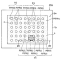
図14に、フラックス残渣5dがFR1〜FR5のいずれかの状態のところにアンダーフィル4が浸透し、硬化された実装構造体MSpの一例を示す。同図は、図11に示す実装構造体MSpからLGAパッケージ2を外し、矢印A方向から見た状態を示している。一部の端子11からは配線が引き出されているが、図14では、見易さを考慮して配線を省略している。
FIG. 14 shows an example of the mounting structure MSp in which the
本例においては、フラックス残渣5dは、回路基板1pの実装面Sm上の3つ領域(R1、R2、R3)に拡散している。フラックス拡散領域R1は10個の半田接合部3(端子11)の周囲に拡散し、フラックス拡散領域R2およびR3はそれぞれ3個の半田接合部3(端子11)の周囲に拡散している。
In this example, the
図15に、図14に示した、アンダーフィル4が充填硬化済みの実装構造体MSpをXV−XV線に沿って切断した断面を示す。図15において、左端に示すフラックス拡散領
域R1から外れた領域は、フラックス残渣5dがFR1の状態にある領域、つまり端子11上を除いてフラックス残渣5dが存在しない領域である。よって、回路基板1pおよびLGAパッケージ2はアンダーフィル4によって接着され、また半田接合部3はアンダーフィル4によって形状が保持されている。このような領域をフラックス残渣領域P(FR1)と呼ぶ。
FIG. 15 shows a cross section of the mounting structure MSp shown in FIG. 14 that has been filled and cured with the
フラックス拡散領域R1の端部に位置する半田接合部3の周囲には、FR2の状態のフラックス残渣5dが広がる。つまり、フラックス残渣5dの部分的な皮膜が形成される。アンダーフィル4は回路基板1pに部分的に接着し、LGAパッケージ2には完全に接着し、また半田接合部3の形状を保持している。このような領域をフラックス残渣領域P(FR2)と呼ぶ。
A
フラックス拡散領域R1の端部に位置する半田接合部3と隣接する半田接合部3との間には、FR3の状態のフラックス残渣5dが広がる。つまり、回路基板1pはフラックス残渣5dの比較的薄い皮膜によって完全に覆われている。アンダーフィル4はLGAパッケージ2とは完全に接着するが、回路基板1pと接着できない。アンダーフィル4は半田接合部3の形状を保持する。このような領域をフラックス残渣領域P(FR3)と呼ぶ。
Between the solder
フラックス拡散領域R1の中心部に位置する半田接合部3と隣接する半田接合部3の間には、FR4の状態のフラックス残渣5dが広がる。つまり、回路基板1pはフラックス残渣5dの比較的厚い皮膜によって覆われている。アンダーフィル4はLGAパッケージ2とは完全に接着しているが、回路基板1pと接着できていない。アンダーフィル4は、部分的にしか半田接合部3の形状を保持できない。このような領域をフラックス残渣領域P(FR4)と呼ぶ。
Between the
フラックス拡散領域R1の中心部に位置する隣接する半田接合部3の間には、FR5の状態のフラックス残渣5dが広がる。つまり、回路基板1pとLGAパッケージ2との間の空間はフラックス残渣5dによって埋められている。従って、アンダーフィル4は回路基板1pおよびLGAパッケージ2と接着できず、また半田接合部3の形状を保持することもできない。このような領域をフラックス残渣領域P(FR5)と呼ぶ。
Between the
回路基板1p上に、領域P(FR5)のようにフラックス残渣で塞がれた箇所が点在すると、アンダーフィル4が毛細管現象によって浸透する際、フラックス残渣で塞がれた箇所を避けるようにして複数の方向から進む。その結果、図14の例では示されていないが、場所によっては空気を隙間に閉じ込めて気泡を生成する。閉じ込められた空気(気泡)はアンダーフィル4の加熱硬化時に膨張して、アンダーフィル4を更に排除し、結果的にアンダーフィル4と回路基板1pやLGAパッケージ2との接触面積を狭めることになり、十分な接続強度を確保できなくなる。
If there are spots on the
上述したように、半田から分離したフラックス残渣5dが回路基板1pの端子11間に存在する場合、フラックス残渣5dによってアンダーフィル4の充填が妨げられ、回路基板1pとLGAパッケージ2と間の十分な接続強度を確保できなくなる。またアンダーフィル4による半田接合部3の形状保持機能も十分発揮できなくなる。
As described above, when the
上述の問題点を解決する方法として、リフロー処理による半田付け工程が終了した後に、実装構造体MSpを洗浄してフラックス残渣を除去することが考えられる。しかし、フラックス残渣の洗浄は製造工程を複雑にし、またフラックス残渣の洗浄で生じる物質は環境汚染の原因となる。そのため、フラックス残渣を洗浄しないで半田付けを行うことが望ましい。 As a method for solving the above-described problems, it is conceivable to remove the flux residue by cleaning the mounting structure MSp after the soldering process by the reflow process is completed. However, cleaning the flux residue complicates the manufacturing process, and substances generated by cleaning the flux residue cause environmental pollution. Therefore, it is desirable to perform soldering without cleaning the flux residue.
フラックス残渣を洗浄しないまま、回路基板とパッケージとの間にアンダーフィルを充填し、しかも十分な接続強度を確保する手段として、回路基板を貫通する通気孔を設けることが提案されている(特許文献1参照)。
しかし、半田から分離したフラックスは液体であり、フラックス源(半田接合部)から通気孔までの間を液状のフラックスが移動する。つまり回路基板上をフラックスが拡散し、通過した跡にフラックス残渣が残る。 However, the flux separated from the solder is liquid, and the liquid flux moves from the flux source (solder joint) to the vent hole. That is, the flux diffuses on the circuit board, and a flux residue remains on the trace that has passed.
またフラックス残渣の残留を抑制するためには、通気孔の数を多くし、さらに通気孔の径を大きくする必要がある。しかし、液状フラックスの排出が促進できたとしても、アンダーフィルの充填工程において、通気孔からアンダーフィルが外部に排出されることになる。その結果、回路基板と電子部品との接続強度を補強するのに十分な量のアンダーフィルを確保できなくなる恐れがある。 In order to suppress the residue of the flux residue, it is necessary to increase the number of vent holes and further increase the diameter of the vent holes. However, even if the discharge of the liquid flux can be promoted, the underfill is discharged to the outside from the vent hole in the underfill filling process. As a result, there is a fear that a sufficient amount of underfill to reinforce the connection strength between the circuit board and the electronic component cannot be secured.
そこで本発明は、回路基板と電子部品との間のアンダーフィルによる接続強度を確保し、ひいてはランドと端子との間の安定した電気的接続を実現できる実装構造体を提供することを目的とする。 SUMMARY OF THE INVENTION Accordingly, an object of the present invention is to provide a mounting structure that can secure connection strength due to underfill between a circuit board and an electronic component, and thus can realize stable electrical connection between a land and a terminal. .
本発明は、下面に複数のランドが設けられた平板状の電子部品と、実装面に前記複数のランドに対応する複数の端子が設けられた回路基板とを備え、前記複数のランドと前記複数の端子が、それぞれ半田により接合された実装構造体であって、
前記回路基板は、さらに前記半田から分離したフラックスを収容するフラックス収容手段を備え、前記フラックス収容手段は、前記複数の端子の少なくとも1つを囲むダミー電極であり、前記電子部品の下面と前記回路基板の実装面とは、その間に充填されたアンダーフィルで接続されている、実装構造体に関する。あるいは、本発明は、下面に複数のランドが設けられた平板状の電子部品と、実装面に前記複数のランドに対応する複数の端子が設けられた回路基板とを備え、前記複数のランドと前記複数の端子が、それぞれ半田により接合された実装構造体であって、前記回路基板は、さらに前記半田から分離したフラックスを収容するフラックス収容手段を備え、前記フラックス収容手段は、前記複数の端子の少なくとも1つを囲む、前記回路基板に設けられた壁により囲まれた部分、または前記回路基板に設けられた溝であり、前記電子部品の下面と前記回路基板の実装面は、その間に充填されたアンダーフィルで接続されている、実装構造体に関する。あるいは、本発明は、平板状の電子部品とで実装構造体を構成し、かつ実装面に、前記平板状の電子部品の下面に設けられた複数のランドのそれぞれに対応する複数の端子が設けられた回路基板であって、前記複数のランドと複数の端子との接合に用いられる半田から分離したフラックスを収容するフラックス収容手段を備え、前記フラックス収容手段は、前記複数の端子の少なくとも1つを囲むダミー電極であり、前記電子部品の下面と前記回路基板の実装面は、その間に充填されたアンダーフィルで接続されている、回路基板に関する。あるいは、本発明は、平板状の電子部品とで実装構造体を構成し、かつ実装面に、前記平板状の電子部品の下面に設けられた複数のランドのそれぞれに対応する複数の端子が設けられた回路基板であって、前記複数のランドと複数の端子との接合に用いられる半田から分離したフラックスを収容するフラックス収容手段を備え、前記フラックス収容手段は、前記複数の端子の少なくとも1つを囲む、前記回路基板に設けられた壁により囲まれた部分、または前記回路基板に設けられた溝であり、前記電子部品の下面と前記回路基板の実装面とは、その間に充填されたアンダーフィルで接続されている、回路基板に関する。
The present invention includes a flat plate-like electronic component having a plurality of lands on a lower surface, and a circuit board having a plurality of terminals corresponding to the plurality of lands on a mounting surface, the plurality of lands and the plurality of lands. Each of the terminals is a mounting structure joined by solder,
The circuit board may further include a flux containing means for containing the separate flux from the solder, the flux receiving means, Ri dummy electrodes der surrounding at least one of said plurality of terminals, the lower surface of the electronic component The mounting surface of the circuit board relates to a mounting structure that is connected by an underfill filled therebetween. Alternatively, the present invention comprises a flat plate-like electronic component having a plurality of lands on a lower surface, and a circuit board having a plurality of terminals corresponding to the plurality of lands on a mounting surface, and the plurality of lands The plurality of terminals are each a mounting structure joined by solder, and the circuit board further includes flux accommodating means for accommodating a flux separated from the solder, and the flux accommodating means includes the plurality of terminals. A portion surrounded by a wall provided on the circuit board, or a groove provided on the circuit board, and the lower surface of the electronic component and the mounting surface of the circuit board are filled between them. The mounting structure is connected with an underfill. Alternatively, according to the present invention, a mounting structure is configured with a flat plate-like electronic component, and a plurality of terminals corresponding to each of a plurality of lands provided on the bottom surface of the flat plate-like electronic component are provided on the mounting surface. And a flux accommodating means for accommodating a flux separated from the solder used for joining the plurality of lands and the plurality of terminals, wherein the flux accommodating means is at least one of the plurality of terminals. The lower surface of the electronic component and the mounting surface of the circuit board are connected to each other by an underfill filled therebetween. Alternatively, according to the present invention, a mounting structure is configured with a flat plate-like electronic component, and a plurality of terminals corresponding to each of a plurality of lands provided on the bottom surface of the flat plate-like electronic component are provided on the mounting surface. And a flux accommodating means for accommodating a flux separated from the solder used for joining the plurality of lands and the plurality of terminals, wherein the flux accommodating means is at least one of the plurality of terminals. A portion surrounded by a wall provided on the circuit board, or a groove provided on the circuit board, and an under surface filled between the lower surface of the electronic component and the mounting surface of the circuit board The circuit board is connected by a fill.
前記ダミー電極の表面が、ソルダーレジスト膜で覆われていてもよい。 Surface prior Symbol dummy electrodes may be covered with a solder resist film.
前記電子部品の下面と前記回路基板の実装面は、その間に充填されたアンダーフィルで接続されていることが好ましく、また前記半田は、その側面形状にそって硬化された前記アンダーフィルによって固定されていることが好ましい。 The lower surface of the electronic component and the mounting surface of the circuit board are preferably connected with an underfill filled therebetween, and the solder is fixed by the underfill cured along the side surface shape. It is preferable.
本発明にかかる実装構造体は、リフロー処理時に、半田から滲み出したフラックスが回路基板の実装面上を拡がるのを抑制できる。結果として、回路基板と電子部品との間のアンダーフィルによる十分な接続強度を確保できる。 The mounting structure according to the present invention can suppress the flux oozing from the solder from spreading on the mounting surface of the circuit board during the reflow process. As a result, sufficient connection strength due to underfill between the circuit board and the electronic component can be secured.
本発明の実施の形態にかかる実装構造体のそれぞれについて詳述する前に、本発明にかかる実装構造体の特徴について説明する。本発明の実装構造体は、回路基板を除いて上述の従来の実装構造体と同様の構成を有している。本発明の回路基板には、従来の回路基板が有しない、リフロー処理時に半田から分離するフラックスを収納する手段が設けられている。 Before describing each of the mounting structures according to the embodiments of the present invention in detail, the features of the mounting structure according to the present invention will be described. The mounting structure of the present invention has the same configuration as the above-described conventional mounting structure except for the circuit board. The circuit board of the present invention is provided with means for storing a flux that is separated from solder during reflow processing, which the conventional circuit board does not have.
同手段により、回路基板の実装面と電子部品の下面との隙間にフラックスが拡がるのを抑えられる。その結果、回路基板の実装面、およびLGAパッケージの下面に対するアンダーフィルの接触面積を確保できる。これにより、回路基板と電子部品との間の接続強度を補強するというアンダーフィルの機能が十分発揮される。 By this means, it is possible to suppress the flux from spreading in the gap between the mounting surface of the circuit board and the lower surface of the electronic component. As a result, the contact area of the underfill to the mounting surface of the circuit board and the lower surface of the LGA package can be secured. As a result, the underfill function of reinforcing the connection strength between the circuit board and the electronic component is sufficiently exhibited.
以下に、図面を参照して、実施の形態のそれぞれについて詳述する。図中、従来の実装構造体と同一の機能を有する部材には同一の符号を付して説明を省略する。 Hereinafter, each embodiment will be described in detail with reference to the drawings. In the figure, members having the same functions as those of the conventional mounting structure are denoted by the same reference numerals and description thereof is omitted.
(実施の形態1)
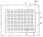
図1、図2および図3を参照して、本発明の実施の形態1にかかる実装構造体について説明する。実施の形態1にかかる実装構造体MSaは、従来の実装構造体MSpと同様に(図11参照)、回路基板1aの実装面にLGAパッケージ2が取り付けられている。図1に、実施の形態1にかかる実装構造体MSaのLGAパッケージ2を外した状態を示す。また図2に、図1のII−II線に沿って切断した実装構造体MSaの要部断面を示す。
(Embodiment 1)
A mounting structure according to a first embodiment of the present invention will be described with reference to FIGS. In the mounting structure MSa according to the first embodiment, the
一部の端子11からは電気接続用の配線が引き出されているが、図1〜図3では、見易さを考慮して配線を省略している。また、回路基板1aの内部には、スルーホールを含む立体的な配線が形成されているが、本発明とは直接関係しないため、省略している。
Although wiring for electrical connection is drawn out from some
マトリクス状に形成されたLGAパッケージ2のランド21と、同じくマトリクス状に形成された回路基板1aの端子11とは半田で接合され、半田接合部3を形成している。通常、ランドの径は0.3〜0.6mm、ランドのピッチは0.5〜1mmである。ランド21は、例えばW/Ni/Auの積層構造をなしており、パッケージの表面から順に、約10μm厚のWと約5μm厚のNiが積層され、その表面が約0.6μm厚のAuメッキで覆われている。端子11は、CuまたはCuに錫、亜鉛、ニッケルまたは金のメッキを施したものであり、その厚みは20〜70μmである。また半田はSnを含む。
The
図1に示すように、回路基板1aの実装面Smには、リフロー処理時に半田接合部3から滲み出してくるフラックス5を収容するリング状の溝12が、端子11の周囲に形成されている。図2に示すように、半田接合部3の表面を伝わって端子11に到達したフラックス5は、溝12の中に流れ込んで収容されるため、回路基板1aの実装面Sm上に拡散することが阻止される。その結果、前述の図13B〜図13Eで説明したFR2〜FR5の状態のフラックス残渣の発生を防止できる。
As shown in FIG. 1, a ring-shaped
リング状溝12の深さD1と幅W1(図2参照)は、フラックス5の量によって調整する必要がある。すなわちリング状の溝12の容積は、1つの半田接合部3から分離されるフラックス5を収容し、かつ実装面上にフラックス5が拡散しない程度の大きさにする必要がある。幅W1をあまり広くすると、アンダーフィル4と回路基板1aとの接触面積が小さくなるため好ましくない。またリング状溝12の深さD1をあまり深くすると、回路基板1aの機械的な強度が弱くなるため好ましくない。通常の仕様のLGAパッケージ2を回路基板1aに実装する場合、リング状溝12の深さD1は5〜50μm、幅W1は50〜500μmであることが好ましい。
The depth D1 and the width W1 (see FIG. 2) of the ring-shaped
次に、実装構造体MSaの製造方法について説明する。最初に回路基板1aの製造方法について説明する。前述したように実装構造体の回路基板には、一般的に、立体的な配線が内部に形成された多層の回路基板が用いられる。多層の回路基板は、プリプレグや銅箔等を積み重ねた後、ドリルやレーザの加工でビアやスルーホールを形成し、レジストで表面を保護することにより作成される。しかし、回路基板の内部構造は、本発明とは直接的には関係しない。そこで説明を分かり易くするため、ここでは、単層の絶縁層を有する回路基板を作成する場合を例に挙げて説明する。
Next, a method for manufacturing the mounting structure MSa will be described. First, a method for manufacturing the
エポキシ樹脂等の耐熱性、誘電特性、絶縁特性および加工性に優れた熱硬化性の樹脂を補強材であるガラス繊維に含浸させてプリプレグを作成する。 A prepreg is prepared by impregnating a glass fiber as a reinforcing material with a thermosetting resin excellent in heat resistance, dielectric properties, insulating properties and workability such as epoxy resin.
次に、プリプレグの一方の面に銅箔を貼り付けた後、プレス機でプリプレグの両面を挟んだ状態で加圧および加熱し、樹脂を硬化させると共に、銅箔を樹脂に固定する。 Next, after a copper foil is attached to one surface of the prepreg, it is pressed and heated with the pressing machine sandwiching both surfaces of the prepreg to cure the resin and fix the copper foil to the resin.
次に、フォトリソグラフィおよびエッチングにより、樹脂基材の表面に貼り付けられた銅箔を加工して、端子11を含む配線パターンを形成する。
Next, the copper foil attached to the surface of the resin base material is processed by photolithography and etching to form a wiring pattern including the
次に、樹脂基材の所定の箇所にレーザ光を照射して、所定の深さのリング状の溝を形成する。このようにして配線パターンおよびリング状溝12が形成された回路基板1aが完成する。
Next, a predetermined portion of the resin base material is irradiated with laser light to form a ring-shaped groove having a predetermined depth. Thus, the
次に、このようにして作成された回路基板1aの端子11上に、スクリーン印刷によって半田ペーストを塗布し、更にその上にLGAパッケージ2を、ランド21が端子11に対向する状態で載置する。
Next, a solder paste is applied by screen printing on the
このようにして、回路基板1aにLGAパッケージ2が仮止めされた実装構造体MSaを、リフロー処理することにより、回路基板1aの端子11とLGAパッケージ2のランド21が半田によって接合される。
In this way, the mounting structure MSa in which the
次に、回路基板1aとLGAパッケージ2との隙間にアンダーフィル4を充填する。前述の図11で説明したのと同様に、アンダーフィル4の溶液を、回路基板1aとLGAパッケージ2の境に滴下する。通常、アンダーフィル4の粘度は10Pa・s以下である。塗布時にアンダーフィル4を摂氏数十度まで加熱しても良い。
Next, the
液状のアンダーフィル4は、毛細管現象によって回路基板1aとLGAパッケージ2との間に浸透して拡がる。この際、フラックス残渣5dは端子11の周囲に形成されたリング状溝12に収容されているため、アンダーフィル4の浸透を妨げない。回路基板1aとLGAパッケージ2との間に浸透したアンダーフィル4は、その後加熱され硬化して、回路基板1aとLGAパッケージ2を機械的に接続し、また半田接合部3の形状を保持するように機能する。このようにして実装構造体MSaが完成する。
The
図3に、本実施の形態の実装構造体MSaの変形例を示す。図3は、図2の回路基板1
aを回路基板1bに置き換えたものである。回路基板1bでは、フラックス5を収容する手段として、端子11を取り囲むようにリング状の壁13が設けられている。リング状壁13は長方形の断面を有するように形成されている。
FIG. 3 shows a modification of the mounting structure MSa of the present embodiment . 3 shows the
a is replaced with the
リング状壁13の機能はリング状溝12のそれと変わらない。すなわち、半田ペーストの加熱時に、半田接合部3から分離したフラックス5をリング状壁13で囲まれた部分に収容し、フラックス5が隣接する端子11との間に拡散するのを防止する。リング状壁13の高さH1や端子11との間の間隔S1は、リング状溝12と同様に、収容するフラックスの量に従って適宜設定される。
The function of the ring-shaped
回路基板1bの実装面Smに壁13を形成する方法について簡単に説明する。通常、回路基板1bの配線パターンは、回路基板1bの実装面Smに貼り付けた銅箔にフォトリソグラフィ処理およびエッチング処理を施すことにより形成される。この際、銅箔の一部を残すことにより、壁13を併せて形成できる。
A method for forming the
(実施の形態2)
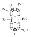
図4および図5を参照して、本発明の実施の形態2にかかる実装構造体について説明する。図4に、図1と同様に本実施の形態にかかる実装構造体MScのLGAパッケージ2を外した状態を示す。また図5に、図4のV−V線に沿って切断した実装構造体MScの要部断面を示す。
(Embodiment 2)
Referring to FIGS. 4 and 5, will be described mounting structure according to a second embodiment of the present invention. FIG. 4 shows a state where the
実施の形態1では、フラックス残渣5dを収容する手段として、回路基板1aの端子11の周りに形成したリング状溝、もしくは回路基板1bの端子11の周りに形成したリング状壁13で囲まれた空間を用いている。
In the first embodiment, the means for containing the
これに対し本実施の形態では、フラックス5を収容する手段として、隣り合う2つのリング状溝が1つの長方形の溝で連結された連結溝14を用いている。連結溝14において、リング状溝12に相当する2つのリング状溝部14−1が連結溝部14−2によって接続されている。
On the other hand, in the present embodiment , as a means for accommodating the
リング状溝12(図1参照)で収容しきれないほどの大量のフラックスでも、リング状溝部14−1を介して連結溝部14−2に導かれて、連結溝14の全体で収容できる。つまり、リング状溝部14−1の容量がリング状溝12の容量と同じであれば、連結溝14の容量はリング状溝12に比べて連結溝部14−2の1/2だけ大きくできる。言い換えれば、連結溝部14−2の1/2だけリング状溝部14−1の容量を小さくして、連結溝14としてはリング状溝12と同じ容量にできる。
Even a large amount of flux that cannot be accommodated in the ring-shaped groove 12 (see FIG. 1) is guided to the connecting groove part 14-2 via the ring-shaped groove part 14-1, and can be accommodated in the entire connecting
リング状溝部14−1から溢れたフラックス5をこの長方形状の連結溝部14−2に収容することにより、フラックス5の拡散を防止する効果が高まる。例えば、フラックス残渣5の量が多く、前述の図15に示したように、フラックス残渣領域P(FR2)およびフラックス残渣領域P(FR3)が発生してしまうような場合であっても、フラックス5を連結溝部14−2内に閉じこめることによって、これらの領域の発生をより効果的に防止できる。
By accommodating the
図6Aに、図4のVI−VI線に沿って切断した連結溝部14−2の短手方向の断面を
示す。連結溝部14−2は溝壁が回路基板1cの実装面Smに対し概ね直角に形成されている。しかし、連結溝部14−2の溝壁は、図6Bに示すように回路基板1cの実装面Smに対し鈍角になるように形成しても良い。
FIG. 6A shows a cross-section in the short direction of the connecting groove 14-2 cut along the line VI-VI in FIG. The groove groove of the connecting groove 14-2 is formed substantially at right angles to the mounting surface Sm of the
連結溝14の向きは、特に限定されない。ただし、アンダーフィル4の充填を考慮すると、連結溝14は、その長方方向がアンダーフィル4の浸透方向に平行になるように配置されることが好ましい。この理由について簡単に説明する。
The direction of the connecting
リフロー処理後の実装構造体MScの端部に塗布されたアンダーフィル4は、毛細管現象によって回路基板1cとLGAパッケージ2との間を放射状に浸透しようとする(図11参照)。その際、アンダーフィル4は、回路基板1c上に設けられた連結溝14を迂回して浸透しなければならない。特に、連結溝部14−2がアンダーフィル4の浸透方向に対し直交する方向に配置されている場合、アンダーフィル4の浸透に対して障害として働く。
The
その結果、回路基板1cの中央部と周辺部でアンダーフィル4の浸透速度に差が生じ、異なる方向から浸透するアンダーフィル4によって浸透方向の先端部に空気が閉じ込められる場合がある。空気が閉じ込められた領域ではアンダーフィル4による補強効果を発揮できない。よって、連結溝14を設ける場合には、回路基板1上のアンダーフィル4の浸透速度が場所によって大きく異ならないように考慮する必要がある。
As a result, there is a difference in the permeation speed of the
回路基板1cの作成については、実施の形態1の回路基板1aの作成と同様の方法で作成できるので、説明を省略する。
The creation of the
図7Aおよび図7Bを参照して、連結溝14の変形例について説明する。図7Aに示す変形例では、リング状壁13(図3参照)に相当する2つのリング状壁部15−1が2つの連結壁部15−2で接続されて連結壁15が構成されている。これらの壁で囲まれた空間にフラックス5が収容される。
A modification of the connecting
図7Bに示す例では、連結溝14から2つのリング状溝部14−1が取り除かれている。つまり、連結溝部14−2に相当する矩形溝16が隣り合う2つの端子11を接続するように形成されている。矩形溝16の形状が単純なため製造がしやすい。半田接合部3から分離されるフラックスの量が少ない場合には、このような溝でも、フラックス5を収容する手段として十分な効果を発揮する。連結壁15および矩形溝16の容積は、そこに収容されるフラックス5の量によって適宜設定される。
In the example shown in FIG. 7B, the two ring-shaped groove portions 14-1 are removed from the connecting
(実施の形態3)
図8および図9を参照して、本発明の実施の形態3にかかる実装構造体について説明する。図8に、本実施の形態にかかる実装構造体MSdの一部を四角形状に切り出した部分の平面図を示す。図8に示す実装構造体MSdは、図1のそれと同様にLGAパッケージが外されている。また図9に、図8のIX−IX線に沿って切断した実装構造体MSdの断面を示す。
(Embodiment 3 )
With reference to FIG. 8 and FIG. 9, the mounting
図1に示した実装構造体MSaと同様に、LGAパッケージの下面にはマトリクス状にランド21が形成され、また回路基板1dの実装面Smにもマトリクス状に端子11が形成されている。しかし実装構造体MSaと異なり、回路基板1dに設けられた2つの端子11の間は配線17aで接続され、また一方の端子11からは配線17bが延出している。また端子11、配線17aおよび17bを、間隔を隔てて取り囲むようにダミー電極18が設けられている。さらにダミー電極18の表面はソルダーレジスト膜19で覆われている。
Similarly to the mounting structure MSa shown in FIG. 1, lands 21 are formed in a matrix on the lower surface of the LGA package, and
ダミー電極18は、回路基板1dの実装面Smのうち端子11、配線17aおよび17bを除く領域を銅箔で覆ったものであり、回路基板1dの強度向上および高周波特性の改善を目的として設けられている。高周波特性の改善を目的とする場合は、ダミー電極18は接地される。配線17aおよび17bがない場合には、ダミー電極18は、図3に示したリング状壁13と同様に、端子11を取り囲むように形成される。
The
ソルダーレジスト膜19は、端子11を半田付けする際に、端子11以外の場所に半田が流れないように、銅箔の表面を樹脂で覆ったものである。ソルダーレジスト膜19の厚みは、通常20〜30μmである。
The solder resist
実施の形態1の実装構造体MSaでは、半田から分離したフラックス5を収容する手段をリング状の溝や壁で構成していた。これに対し、本実施の形態の実装構造体MSdでは、フラックスを収容する手段を、端子11を取り囲むように配置されたダミー電極18(更にソルダーレジスト膜19)で構成している。
In the mounting structure MSa of the first embodiment , the means for accommodating the
すなわち本実施の形態の実装構造体MSdは、回路基板の強度向上および高周波特性の改善を目的として設けられたダミー電極18(更にはソルダーレジスト膜19)を、フラックスを収容する手段と兼用している。リフロー処理時に半田接合部3から分離したフラックス5は、ダミー電極18およびソルダーレジスト膜19によって形成された溝の中に流れ込んで収容されるため、フラックスが回路基板1dの実装面Sm上に拡散するのを阻止できる。
That is, the mounting structure MSd of the present embodiment uses the dummy electrode 18 (and also the solder resist film 19) provided for the purpose of improving the strength of the circuit board and the high frequency characteristics as a means for accommodating the flux. Yes. Since the
ソルダーレジスト膜19は、フラックスを収容する手段として不可欠なものではないが、ダミー電極18の表面を一定の厚さで覆うことにより溝の容積が増加する。その意味において、ソルダーレジスト膜19はフラックス収容手段の一部を構成している。
The solder resist
またソルダーレジスト膜19で覆われた回路基板1dの実装面Smのうち、配線17aとダミー電極18、および配線17bとダミー電極18で挟まれた部分にもフラックスを収容できる。この部分はソルダーレジスト膜19により溝の深さが若干浅くなるが、収容するフラックスの量が少なければ問題はない。配線17bとダミー電極18よって形成される溝は、一方(図8では右端)が開放されているため、ここからフラックスが外部に漏れ出す恐れがある。それを避けたい場合には、その部分のソルダーレジスト膜19を厚くするなどの対策が必要となる。
Further, the flux can also be accommodated in the portion of the mounting surface Sm of the
回路基板1dの実装面Smからソルダーレジスト膜19の上面までの高さH2、および端子11とソルダーレジスト膜19との間の間隔S2は、実施の形態1のリング状溝12と同様に、収容するフラックス5の量に従って適宜設定される。
Height H2 to the upper surface of the solder resist
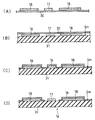
次に、回路基板1dの作成方法について、図10を参照して説明する。最初に配線パターンを形成する。図10の(A)に示すように、離形フィルム30の一方の面に銅箔を接着した後、フォトリソグラフィ工程およびエッチング工程を経て、端子11やダミー電極18を含む配線パターンを形成する。離形フィルム30としては、例えば、ポリエチレンテレフタレートやポリフェニレンサルファイドのフィルムを用いることができる。
Next, a method for producing the
次に、図10の(B)に示すように、あらかじめ作成した回路基材31の実装面Smに、離形フィルム30上に形成された配線パターン(端子11、ダミー電極18)を位置決めした後接着する。その後、離形フィルム30を配線パターンから剥離する。回路基材31の内部には、スルーホールを含む立体的な配線が形成されているが、図では省略している。
Next, as shown in FIG. 10B, after positioning the wiring pattern (
次に、図10の(C)に示すように、配線パターン(端子11、ダミー電極18)が形成された回路基材31の実装面Smに、スクリーン印刷でソルダーレジストを塗布し、一定の厚さのソルダーレジスト膜19を形成する。
Next, as shown in FIG. 10C, a solder resist is applied by screen printing to the mounting surface Sm of the
次に、図10の(D)に示すように、フォトリソグラフィ工程およびエッチング工程を経て、端子11上に形成されたソルダーレジスト膜19を除去する。
Next, as shown in FIG. 10D, the solder resist
このようにして作成された回路基板1dに、実施の形態1で説明したのと同様の方法で、LGAパッケージ2を半田付けして、実装構造体MSdを完成させる。
This way, the
このように本実施の形態の実装構造体MSdは、回路基板の強度向上および高周波特性の改善を目的として設けられたダミー電極18(更にはソルダーレジスト膜19)を、フラックスを収容する手段として兼用しており、回路基板1dを作成する際に新たな工程を付加する必要がないため、実装構造体MSdの製造コストを抑える観点より、そのメリットは大きい。
As described above, the mounting structure MSd of the present embodiment also uses the dummy electrode 18 (and the solder resist film 19) provided for the purpose of improving the strength of the circuit board and improving the high frequency characteristics as a means for containing the flux. In addition, since it is not necessary to add a new process when creating the
以上説明したように、本発明にかかる実装構造体は、リフロー処理時に半田から分離するフラックスを収容する手段として、回路基板の実装面に設けられたダミー電極を利用している。これにより、既存の実装構造体に簡単な構成を付加し、もしくは既存の実装構造体の形状を若干変更するだけで、フラックスが回路基板の実装面上に拡がるのを防止できる。その結果、アンダーフィルによる回路基板と電子部品との十分な接続強度を確保し、またアンダーフィルによる半田接合部の形状保持機能を実現する。 As described above, the mounting structure according to the present invention uses the dummy electrode provided on the mounting surface of the circuit board as means for accommodating the flux that is separated from the solder during the reflow process . Thereby , it is possible to prevent the flux from spreading on the mounting surface of the circuit board only by adding a simple configuration to the existing mounting structure or by slightly changing the shape of the existing mounting structure. As a result, sufficient connection strength between the circuit board and the electronic component by underfill is ensured, and the shape maintaining function of the solder joint by underfill is realized.
上述した実施の形態では、電子部品としてLGAパッケージを用いる場合について説明したが、本発明はこれに限定されず、BGA(ボール・グリッド・アレイ)やCSP(チップ・サイズ・パッケージ)等の他のパッケージを用いた電子部品にも適用されることは云うまでもない。 In the form of implementation described above, description has been given of the case using the LGA package as an electronic component, the present invention is not limited to this, BGA (ball grid array), CSP etc. (Chip Size Package) Needless to say, the present invention can be applied to electronic components using other packages.
本発明は、回路基板上にLGA、BGA、CSP等の表面実装型の電子部品が実装された実装構造体に広く適用できる。 The present invention can be widely applied to mounting structures in which surface-mounted electronic components such as LGA, BGA, and CSP are mounted on a circuit board.
MSa〜MSd 実装構造体
1a〜1d 回路基板
2 LGAパッケージ
3 半田接合部
4 アンダーフィル
5 フラックス
5d フラックス残渣
11 端子
12 リング状溝
13 リング状壁
14 連結溝
15 連結壁
16 矩形溝
17a、17b 配線
18 ダミー電極
19 ソルダーレジスト膜
21 ランド
30 離形フィルム
31 回路基材
MSa-
Claims (8)
実装面に前記複数のランドに対応する複数の端子が設けられた回路基板とを備え、
前記複数のランドと前記複数の端子が、それぞれ半田により接合された実装構造体であって、
前記回路基板は、さらに前記半田から分離したフラックスを収容するフラックス収容手段を備え、
前記フラックス収容手段は、前記複数の端子の少なくとも1つを囲むダミー電極であり、
前記電子部品の下面と前記回路基板の実装面とは、その間に充填されたアンダーフィルで接続されている、実装構造体。 A flat electronic component having a plurality of lands on the lower surface;
A circuit board provided with a plurality of terminals corresponding to the plurality of lands on the mounting surface;
The plurality of lands and the plurality of terminals are each a mounting structure joined by solder,
The circuit board further includes flux accommodating means for accommodating the flux separated from the solder,
The flux receiving means, Ri dummy electrodes der surrounding at least one of said plurality of terminals,
A mounting structure in which a lower surface of the electronic component and a mounting surface of the circuit board are connected by an underfill filled therebetween.
実装面に前記複数のランドに対応する複数の端子が設けられた回路基板とを備え、A circuit board provided with a plurality of terminals corresponding to the plurality of lands on the mounting surface;
前記複数のランドと前記複数の端子が、それぞれ半田により接合された実装構造体であって、The plurality of lands and the plurality of terminals are each a mounting structure joined by solder,
前記回路基板は、さらに前記半田から分離したフラックスを収容するフラックス収容手段を備え、The circuit board further includes flux accommodating means for accommodating the flux separated from the solder,
前記フラックス収容手段は、前記複数の端子の少なくとも1つを囲む、前記回路基板に設けられた壁により囲まれた部分、または前記回路基板に設けられた溝であり、The flux accommodating means is a portion surrounded by a wall provided in the circuit board, surrounding at least one of the plurality of terminals, or a groove provided in the circuit board,
前記電子部品の下面と前記回路基板の実装面は、その間に充填されたアンダーフィルで接続されている、実装構造体。 A mounting structure in which a lower surface of the electronic component and a mounting surface of the circuit board are connected by an underfill filled therebetween.
前記複数のランドと複数の端子との接合に用いられる半田から分離したフラックスを収容するフラックス収容手段を備え、
前記フラックス収容手段は、前記複数の端子の少なくとも1つを囲むダミー電極であり、
前記電子部品の下面と前記回路基板の実装面は、その間に充填されたアンダーフィルで接続されている、回路基板。 A circuit board comprising a mounting structure with a flat electronic component, and a mounting surface provided with a plurality of terminals corresponding to a plurality of lands provided on the lower surface of the flat electronic component. And
Flux containing means for containing flux separated from solder used for joining the plurality of lands and the plurality of terminals,
The flux receiving means, Ri dummy electrodes der surrounding at least one of said plurality of terminals,
The lower surface and the mounting surface of the circuit board of the electronic components, it is connected with an underfill filled between them, the circuit board.
前記複数のランドと複数の端子との接合に用いられる半田から分離したフラックスを収容するフラックス収容手段を備え、Flux containing means for containing flux separated from solder used for joining the plurality of lands and the plurality of terminals,
前記フラックス収容手段は、前記複数の端子の少なくとも1つを囲む、前記回路基板に設けられた壁により囲まれた部分、または前記回路基板に設けられた溝であり、The flux accommodating means is a portion surrounded by a wall provided in the circuit board, surrounding at least one of the plurality of terminals, or a groove provided in the circuit board,
前記電子部品の下面と前記回路基板の実装面とは、その間に充填されたアンダーフィルで接続されている、回路基板。The circuit board, wherein the lower surface of the electronic component and the mounting surface of the circuit board are connected by an underfill filled therebetween.
Priority Applications (1)
| Application Number | Priority Date | Filing Date | Title |
|---|---|---|---|
| JP2008279937A JP5153574B2 (en) | 2007-11-05 | 2008-10-30 | Mounting structure |
Applications Claiming Priority (3)
| Application Number | Priority Date | Filing Date | Title |
|---|---|---|---|
| JP2007287673 | 2007-11-05 | ||
| JP2007287673 | 2007-11-05 | ||
| JP2008279937A JP5153574B2 (en) | 2007-11-05 | 2008-10-30 | Mounting structure |
Publications (3)
| Publication Number | Publication Date |
|---|---|
| JP2009135470A JP2009135470A (en) | 2009-06-18 |
| JP2009135470A5 JP2009135470A5 (en) | 2011-09-22 |
| JP5153574B2 true JP5153574B2 (en) | 2013-02-27 |
Family
ID=40587895
Family Applications (1)
| Application Number | Title | Priority Date | Filing Date |
|---|---|---|---|
| JP2008279937A Expired - Fee Related JP5153574B2 (en) | 2007-11-05 | 2008-10-30 | Mounting structure |
Country Status (4)
| Country | Link |
|---|---|
| US (1) | US8138426B2 (en) |
| JP (1) | JP5153574B2 (en) |
| KR (1) | KR101138599B1 (en) |
| CN (1) | CN101431867B (en) |
Families Citing this family (20)
| Publication number | Priority date | Publication date | Assignee | Title |
|---|---|---|---|---|
| JP5627097B2 (en) * | 2009-10-07 | 2014-11-19 | ルネサスエレクトロニクス株式会社 | Wiring board |
| KR20110041179A (en) * | 2009-10-15 | 2011-04-21 | 한국전자통신연구원 | Structure for packaging |
| US8536672B2 (en) * | 2010-03-19 | 2013-09-17 | Xintec, Inc. | Image sensor package and fabrication method thereof |
| JP5807145B2 (en) * | 2010-05-20 | 2015-11-10 | パナソニックIpマネジメント株式会社 | Mounting structure |
| US20120002386A1 (en) * | 2010-07-01 | 2012-01-05 | Nokia Corporation | Method and Apparatus for Improving the Reliability of Solder Joints |
| WO2012147352A1 (en) * | 2011-04-26 | 2012-11-01 | パナソニック株式会社 | Solar battery cell, junction structure, and solar battery cell fabrication method |
| US10261370B2 (en) | 2011-10-05 | 2019-04-16 | Apple Inc. | Displays with minimized border regions having an apertured TFT layer for signal conductors |
| US9171818B2 (en) * | 2011-12-13 | 2015-10-27 | Cyntec Co., Ltd. | Package structure and the method to manufacture thereof |
| JP5516696B2 (en) * | 2012-11-01 | 2014-06-11 | 株式会社豊田自動織機 | substrate |
| FR2998710B1 (en) | 2012-11-29 | 2016-02-05 | Commissariat Energie Atomique | IMPROVED METHOD OF MAKING A STRUCTURE FOR THE ASSEMBLY OF MICROELECTRONIC DEVICES |
| CN107278029A (en) | 2012-12-21 | 2017-10-20 | 华为终端有限公司 | Electronic installation and grid array module |
| JP6182928B2 (en) * | 2013-03-27 | 2017-08-23 | セイコーエプソン株式会社 | Semiconductor device |
| JP6362066B2 (en) * | 2013-12-17 | 2018-07-25 | キヤノン株式会社 | Printed circuit board manufacturing method and printed circuit board |
| US9711474B2 (en) * | 2014-09-24 | 2017-07-18 | Taiwan Semiconductor Manufacturing Company Ltd. | Semiconductor package structure with polymeric layer and manufacturing method thereof |
| JP6468054B2 (en) * | 2015-04-28 | 2019-02-13 | 富士通株式会社 | Printed circuit board and shield sheet metal fixing method |
| CN106356353A (en) * | 2015-07-14 | 2017-01-25 | 苏州旭创科技有限公司 | Substrate and substrate-applying welding structure and welding method |
| US10276402B2 (en) * | 2016-03-21 | 2019-04-30 | Taiwan Semiconductor Manufacturing Co., Ltd. | Semiconductor package and manufacturing process thereof |
| CN107293482B (en) * | 2017-06-14 | 2021-03-23 | 成都海威华芯科技有限公司 | Method for manufacturing gate electrode of gallium nitride high electron mobility transistor |
| CN109659291A (en) * | 2018-12-24 | 2019-04-19 | 烟台艾睿光电科技有限公司 | A kind of welding ring anti-overflow structure |
| JP7491209B2 (en) | 2020-12-22 | 2024-05-28 | 株式会社デンソー | Electrical component |
Family Cites Families (19)
| Publication number | Priority date | Publication date | Assignee | Title |
|---|---|---|---|---|
| JP3080512B2 (en) * | 1993-05-21 | 2000-08-28 | 株式会社日立製作所 | Wiring board for mounting surface mount components and component mounting connection method |
| JPH07283493A (en) * | 1994-04-14 | 1995-10-27 | Nippon Chemicon Corp | Circuit board with function for preventing flux residue sticking |
| JP3346263B2 (en) * | 1997-04-11 | 2002-11-18 | イビデン株式会社 | Printed wiring board and manufacturing method thereof |
| JPH11145176A (en) | 1997-11-11 | 1999-05-28 | Fujitsu Ltd | Method for forming solder bump and method for forming preliminary solder |
| JP3700598B2 (en) | 2001-03-21 | 2005-09-28 | セイコーエプソン株式会社 | Semiconductor chip, semiconductor device, circuit board, and electronic equipment |
| JP3692978B2 (en) * | 2001-07-24 | 2005-09-07 | 日立電線株式会社 | Wiring board manufacturing method |
| JP4200274B2 (en) | 2002-07-26 | 2008-12-24 | パナソニック電工株式会社 | 3D circuit board electrode terminal structure |
| JP2004103928A (en) * | 2002-09-11 | 2004-04-02 | Fujitsu Ltd | Substrate, forming method of solder ball, and mounting structure thereof |
| JP3631230B2 (en) | 2002-11-21 | 2005-03-23 | 富士通株式会社 | Method for forming spare solder |
| TWI222192B (en) * | 2003-09-04 | 2004-10-11 | Advanced Semiconductor Eng | Substrate with net structure |
| US7126164B2 (en) * | 2003-09-26 | 2006-10-24 | Flipchip International Llc | Wafer-level moat structures |
| KR100555706B1 (en) | 2003-12-18 | 2006-03-03 | 삼성전자주식회사 | ??? for fine pitch solder ball and flip-chip package method using the UBM |
| US7575955B2 (en) * | 2004-01-06 | 2009-08-18 | Ismat Corporation | Method for making electronic packages |
| US20050151268A1 (en) * | 2004-01-08 | 2005-07-14 | Boyd William D. | Wafer-level assembly method for chip-size devices having flipped chips |
| JP4060806B2 (en) * | 2004-01-09 | 2008-03-12 | 日本オプネクスト株式会社 | Connection structure between rigid circuit board and flexible board, connection method, and circuit module using the same |
| JP2006269772A (en) * | 2005-03-24 | 2006-10-05 | Nec Saitama Ltd | Semiconductor package, wiring board, and semiconductor device |
| JP2006294835A (en) | 2005-04-11 | 2006-10-26 | Seiko Epson Corp | Printed circuit board and its forming method |
| JP2007220940A (en) | 2006-02-17 | 2007-08-30 | Matsushita Electric Ind Co Ltd | Printed circuit board and semiconductor device |
| JP5264585B2 (en) * | 2009-03-24 | 2013-08-14 | パナソニック株式会社 | Electronic component joining method and electronic component |
-
2008
- 2008-10-30 JP JP2008279937A patent/JP5153574B2/en not_active Expired - Fee Related
- 2008-10-30 US US12/261,368 patent/US8138426B2/en not_active Expired - Fee Related
- 2008-11-04 KR KR1020080108889A patent/KR101138599B1/en not_active IP Right Cessation
- 2008-11-05 CN CN200810174448XA patent/CN101431867B/en not_active Expired - Fee Related
Also Published As
| Publication number | Publication date |
|---|---|
| KR101138599B1 (en) | 2012-05-10 |
| CN101431867A (en) | 2009-05-13 |
| US20090116203A1 (en) | 2009-05-07 |
| KR20090046712A (en) | 2009-05-11 |
| CN101431867B (en) | 2011-03-09 |
| JP2009135470A (en) | 2009-06-18 |
| US8138426B2 (en) | 2012-03-20 |
Similar Documents
| Publication | Publication Date | Title |
|---|---|---|
| JP5153574B2 (en) | Mounting structure | |
| US8697492B2 (en) | No flow underfill | |
| JP6139653B2 (en) | Component built-in resin multilayer board | |
| JP2008147598A (en) | Stacked package, and method for manufacturing the same | |
| KR20160086181A (en) | Printed circuit board, package and method of manufacturing the same | |
| KR20110128227A (en) | Multilayer printed circuit board and method of making same | |
| JP2011103441A (en) | Semiconductor device and method of manufacturing the same | |
| KR20110040756A (en) | Printed-circuit board, printed-circuit board manufacturing method, and electronic device | |
| JP2011146510A (en) | In-component board, and electronic circuit module | |
| US8357861B2 (en) | Circuit board, and chip package structure | |
| JP6394129B2 (en) | Electronic component built-in module | |
| US20140118984A1 (en) | Electronic device and method of manufacturing the same | |
| JP5587804B2 (en) | Manufacturing method of wiring board for mounting electronic component, wiring board for mounting electronic component, and manufacturing method of wiring board with electronic component | |
| KR101627244B1 (en) | semiconductor pakage | |
| JP2005347414A (en) | Adhesive sheet, and double printed board or multilayer printed board using the same | |
| JP5250502B2 (en) | Semiconductor device and manufacturing method thereof | |
| WO2018110381A1 (en) | Electronic module | |
| WO2010125858A1 (en) | Multilayered resin circuit board, and manufacturing method of multilayered resin circuit board | |
| CN213586442U (en) | Electronic circuit assembly | |
| JP2008311508A (en) | Electronic component package and manufacturing method thereof | |
| JP2018098284A (en) | Circuit board, manufacturing method of circuit board and electronic device | |
| US20220071015A1 (en) | Circuit board structure and manufacturing method thereof | |
| JP2008210825A (en) | Mounting structure and method of electronic component | |
| JP5857249B2 (en) | Mounting structure for semiconductor components | |
| JP4543316B2 (en) | Electronic circuit module component and manufacturing method thereof |
Legal Events
| Date | Code | Title | Description |
|---|---|---|---|
| A521 | Written amendment |
Free format text: JAPANESE INTERMEDIATE CODE: A523 Effective date: 20110808 |
|
| A621 | Written request for application examination |
Free format text: JAPANESE INTERMEDIATE CODE: A621 Effective date: 20110808 |
|
| A131 | Notification of reasons for refusal |
Free format text: JAPANESE INTERMEDIATE CODE: A131 Effective date: 20120906 |
|
| A521 | Written amendment |
Free format text: JAPANESE INTERMEDIATE CODE: A523 Effective date: 20121022 |
|
| TRDD | Decision of grant or rejection written | ||
| A01 | Written decision to grant a patent or to grant a registration (utility model) |
Free format text: JAPANESE INTERMEDIATE CODE: A01 Effective date: 20121108 |
|
| A61 | First payment of annual fees (during grant procedure) |
Free format text: JAPANESE INTERMEDIATE CODE: A61 Effective date: 20121204 |
|
| FPAY | Renewal fee payment (event date is renewal date of database) |
Free format text: PAYMENT UNTIL: 20151214 Year of fee payment: 3 |
|
| R150 | Certificate of patent or registration of utility model |
Free format text: JAPANESE INTERMEDIATE CODE: R150 |
|
| LAPS | Cancellation because of no payment of annual fees |