JP5136996B2 - プログラマブルマスクを基板上に撮像するための方法および装置 - Google Patents
プログラマブルマスクを基板上に撮像するための方法および装置 Download PDFInfo
- Publication number
- JP5136996B2 JP5136996B2 JP2010501439A JP2010501439A JP5136996B2 JP 5136996 B2 JP5136996 B2 JP 5136996B2 JP 2010501439 A JP2010501439 A JP 2010501439A JP 2010501439 A JP2010501439 A JP 2010501439A JP 5136996 B2 JP5136996 B2 JP 5136996B2
- Authority
- JP
- Japan
- Prior art keywords
- substrate
- exposure
- edge
- illumination
- intensity
- Prior art date
- Legal status (The legal status is an assumption and is not a legal conclusion. Google has not performed a legal analysis and makes no representation as to the accuracy of the status listed.)
- Active
Links
- 239000000758 substrate Substances 0.000 title claims description 84
- 238000000034 method Methods 0.000 title claims description 76
- 238000003384 imaging method Methods 0.000 title 1
- 238000005286 illumination Methods 0.000 claims description 82
- 230000008569 process Effects 0.000 claims description 41
- 230000003287 optical effect Effects 0.000 claims description 38
- 230000007423 decrease Effects 0.000 claims description 6
- 230000003247 decreasing effect Effects 0.000 claims description 3
- 238000012937 correction Methods 0.000 description 15
- 101100269850 Caenorhabditis elegans mask-1 gene Proteins 0.000 description 12
- 230000005855 radiation Effects 0.000 description 11
- 238000006073 displacement reaction Methods 0.000 description 8
- 239000002131 composite material Substances 0.000 description 6
- 230000005670 electromagnetic radiation Effects 0.000 description 5
- 238000000206 photolithography Methods 0.000 description 4
- 238000004519 manufacturing process Methods 0.000 description 3
- 239000000463 material Substances 0.000 description 3
- 229920002120 photoresistant polymer Polymers 0.000 description 3
- 230000009467 reduction Effects 0.000 description 3
- 238000003491 array Methods 0.000 description 2
- 230000006872 improvement Effects 0.000 description 2
- VYZAMTAEIAYCRO-UHFFFAOYSA-N Chromium Chemical compound [Cr] VYZAMTAEIAYCRO-UHFFFAOYSA-N 0.000 description 1
- 238000004364 calculation method Methods 0.000 description 1
- 230000008859 change Effects 0.000 description 1
- 239000004020 conductor Substances 0.000 description 1
- 230000001419 dependent effect Effects 0.000 description 1
- 238000010586 diagram Methods 0.000 description 1
- 239000000839 emulsion Substances 0.000 description 1
- 238000007429 general method Methods 0.000 description 1
- 238000005259 measurement Methods 0.000 description 1
- 230000010363 phase shift Effects 0.000 description 1
- 238000010561 standard procedure Methods 0.000 description 1
- 238000012546 transfer Methods 0.000 description 1
- 238000011144 upstream manufacturing Methods 0.000 description 1
Images


Classifications
-
- G—PHYSICS
- G03—PHOTOGRAPHY; CINEMATOGRAPHY; ANALOGOUS TECHNIQUES USING WAVES OTHER THAN OPTICAL WAVES; ELECTROGRAPHY; HOLOGRAPHY
- G03F—PHOTOMECHANICAL PRODUCTION OF TEXTURED OR PATTERNED SURFACES, e.g. FOR PRINTING, FOR PROCESSING OF SEMICONDUCTOR DEVICES; MATERIALS THEREFOR; ORIGINALS THEREFOR; APPARATUS SPECIALLY ADAPTED THEREFOR
- G03F7/00—Photomechanical, e.g. photolithographic, production of textured or patterned surfaces, e.g. printing surfaces; Materials therefor, e.g. comprising photoresists; Apparatus specially adapted therefor
- G03F7/70—Microphotolithographic exposure; Apparatus therefor
- G03F7/70691—Handling of masks or workpieces
- G03F7/70791—Large workpieces, e.g. glass substrates for flat panel displays or solar panels
-
- G—PHYSICS
- G03—PHOTOGRAPHY; CINEMATOGRAPHY; ANALOGOUS TECHNIQUES USING WAVES OTHER THAN OPTICAL WAVES; ELECTROGRAPHY; HOLOGRAPHY
- G03F—PHOTOMECHANICAL PRODUCTION OF TEXTURED OR PATTERNED SURFACES, e.g. FOR PRINTING, FOR PROCESSING OF SEMICONDUCTOR DEVICES; MATERIALS THEREFOR; ORIGINALS THEREFOR; APPARATUS SPECIALLY ADAPTED THEREFOR
- G03F7/00—Photomechanical, e.g. photolithographic, production of textured or patterned surfaces, e.g. printing surfaces; Materials therefor, e.g. comprising photoresists; Apparatus specially adapted therefor
- G03F7/70—Microphotolithographic exposure; Apparatus therefor
- G03F7/70216—Mask projection systems
- G03F7/70283—Mask effects on the imaging process
- G03F7/70291—Addressable masks, e.g. spatial light modulators [SLMs], digital micro-mirror devices [DMDs] or liquid crystal display [LCD] patterning devices
-
- G—PHYSICS
- G03—PHOTOGRAPHY; CINEMATOGRAPHY; ANALOGOUS TECHNIQUES USING WAVES OTHER THAN OPTICAL WAVES; ELECTROGRAPHY; HOLOGRAPHY
- G03F—PHOTOMECHANICAL PRODUCTION OF TEXTURED OR PATTERNED SURFACES, e.g. FOR PRINTING, FOR PROCESSING OF SEMICONDUCTOR DEVICES; MATERIALS THEREFOR; ORIGINALS THEREFOR; APPARATUS SPECIALLY ADAPTED THEREFOR
- G03F7/00—Photomechanical, e.g. photolithographic, production of textured or patterned surfaces, e.g. printing surfaces; Materials therefor, e.g. comprising photoresists; Apparatus specially adapted therefor
- G03F7/70—Microphotolithographic exposure; Apparatus therefor
- G03F7/70216—Mask projection systems
- G03F7/70358—Scanning exposure, i.e. relative movement of patterned beam and workpiece during imaging
Landscapes
- Physics & Mathematics (AREA)
- General Physics & Mathematics (AREA)
- Life Sciences & Earth Sciences (AREA)
- Sustainable Development (AREA)
- Exposure And Positioning Against Photoresist Photosensitive Materials (AREA)
- Exposure Of Semiconductors, Excluding Electron Or Ion Beam Exposure (AREA)
Description
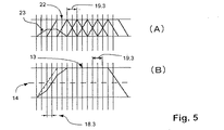
2 基板/イメージ要素
3 照明スポット
4 個々の複写/画素
5 照明ユニット
6 光学ユニット/複写および補正ユニット
7 基板支持体/X−Yテーブル
8 基板カメラ
9 調節カメラ
10 レジストレーションマーク/アライメントマーク
11 Y駆動装置
12 X駆動装置
13 基板/感光層上の合成強度
14 フォトレジスト/感光層の閾値
15 フランク
16 フランクの領域
17 レジストエッジ/構造エッジ
18 レジストエッジ/構造エッジの変位
19 画素グリッド
20 1回目の露光プロセスにおいて書き込まれる個々の強度プロフィール
21 2回目の露光プロセスにおいて書き込まれる個々の強度プロフィール
22 複写要素に対する強度曲線
23 減少した強度を備えた画素
24 電磁放射場
25 電磁放射源
26 変調された放射場
27 ビーム分割器
28 複写光学ユニット
29 画像転写光学ユニット
30 画像偏向器
31 重なり合い領域
32 補正ベクトル
Claims (10)
- 照明スポット(3)が、照明ユニットによって、プログラマブルマスク(1)上に生成され、個々の複写(4)が、光学ユニット(6)を介して、基板(2)上にパターンに対応して生成される、プログラマブルマスク(1)によって生成されるパターンを、感光層を有する基板(2)上に複写するための方法であって、
感光層に対する少なくとも2回の露光プロセスが実行され、前記少なくとも2回の露光プロセスの照明スポット(3)または露光点が、互いにずれて定められること、
露光グリッドが、同じ数の照明スポット(3)または露光点に対して拡張され、露光プロセスの回数が、同じ比で増加させられること、あるいは、露光グリッドが、露光プロセスの回数に対応する特定の倍率だけ拡張され、特に、合計した数の照明スポット(3)または露光点が、基本的に、露光グリッドが拡張されることのない単一露光プロセスの場合と同じ寸法であり、
プログラマブルマスク(1)は、拡大されたテンプレートデータをロードされ、かつ、光学ユニット(6)において、該テンプレートデータは、要求される画像グリッドにまで寸法を縮小され、該テンプレートデータは、基板(2)の要求される画像データおよび/または画像グリッドに対して、特定された、または特定することが可能な倍率によって拡大され、
少なくとも2回の照明プロセスの画像点および/または画素は、構造エッジ(17)に割り当てられおよび/または構造エッジ(17)を生成するためにおよび/または位置決めするために提供される全体強度または合成強度のフランク(15)が基板(2)上において連続的に増加または減少するように、空間的に互いにずれて定められ、
フランク(15)は、構造エッジ(17)を形成するための画素または個々の複写(4)のエッジ領域を重ね合わせることによって生成され、構造エッジ(17)を位置決めするための強度が、上述した画素または個々の複写(4)の中の少なくとも1つに対して減少させられることを特徴とする、方法。 - 露光プロセスが、時間的に連続して実行されることを特徴とする、請求項1に記載の方法。
- 複写されるべきパターンが、複数のプログラマブルマスク(1)内に生成されること、および、露光グリッドが、並列に動作するプログラマブルマスク(1)を用いて、かつ特に可動光学コンポーネントを用いて、同時に実行される露光プロセスの回数と同じ比で増加させられることを特徴とする、請求項1に記載の方法。
- 同時に複写されるマスクパターンが、同じ基板位置または異なる基板位置へ投影されることを特徴とする、請求項3に記載の方法。
- 構造エッジ(17)を生成するために提供される照明スポット(3a)および/または画素(23)の強度が変化させられ、特に、構造を生成するために提供されるその他の照明スポット(3)および/または画素と比較して、減少させられることを特徴とする、請求項1から4のいずれか一項に記載の方法。
- 基板(2)上に複写される画素の合成強度(13)が、連続的な傾斜を有する領域(16)が基板(2)の感光層の閾値(14)との明確な交点を形成するように定められたフランク(15)を有し、前記交点が、関連する照明スポット(3a)および/またはエッジ画素(23)の強度を変化および/または減少させることによって定められ、感光層のエッジしたがって構造エッジ(17)の正確な位置決めが、定められることを特徴とする、請求項1から5のいずれか一項に記載の方法。
- 構造エッジ(17)を変位させ(18)および/または位置決めするために、構造を生成するために定められるエッジ画素(23)および/または構造エッジを生成するために提供されるエッジ照明スポット(3a)の強度が、構造を生成するために提供されるその他の照明スポット(3)の強度に対して、変化特に減少させられることを特徴とする、請求項1から6のいずれか一項に記載の方法。
- 複写されるべきパターンが、プログラマブルマスク(1)内におけるセグメント単位でおよび/またはプログラマブルマスク(1)によるセグメント単位で生成され、照明ユニット(5)および光学ユニット(6)によって、特に、可動コンポーネントによって、歪みを補償する形で基板(2)上に複写され、その結果として、セグメント複写がテンプレート全体を表現すること、および/または、複写されるべきパターンが、光学ユニット(6)によってセグメント単位で基板(2)上に複写され、その結果として、予め検出された歪みが補償されることを特徴とする、請求項1から7のいずれか一項に記載の方法。
- プログラマブルマスク(1)を含み、前記プログラマブルマスク(1)によって、パターンが生成されることが可能であり、前記パターンが、基板(2)の感光層上に複写されることが可能であり、照明スポット(3)が、照明ユニットによってマスク(1)上に生成され、個々の複写(4)が、光学ユニット(6)を介して、基板(2)上にパターンに対応して生成される、請求項1から8のいずれか一項に記載の方法を実行するための装置であって、
感光層に対する少なくとも2回の露光プロセスが実行され、前記少なくとも2回の露光プロセスの照明スポット(3)または露光点が、互いにずれて定められることと、
露光グリッドが、同じ数の照明スポット(3)または露光点に対して、かつ、特に、同じ比の露光プロセス回数で拡張されることとを特徴とする、装置。 - 構造エッジ(17)を位置決めするために、レジストエッジを生成するために提供される1つまたは複数の画素(3a、23)だけが、前記画素の強度を変化させられ、特に、前記画素の強度が減少させられ、このために、少なくとも2回の露光プロセスが同じ感光層において実行され、一方の露光プロセスの照明スポット(3)および/または画素(4)が、他方の露光プロセスの照明スポット(3)および/または画素(4)に対して、空間的に互いにずれて定められる、請求項9に記載の装置の使用。
Applications Claiming Priority (3)
| Application Number | Priority Date | Filing Date | Title |
|---|---|---|---|
| DE102007016926.6 | 2007-04-05 | ||
| DE102007016926 | 2007-04-05 | ||
| PCT/EP2008/002710 WO2008122419A1 (de) | 2007-04-05 | 2008-04-04 | Verfahren und vorrichtung zum abbilden einer programmierbaren maske auf einem substrat |
Publications (2)
| Publication Number | Publication Date |
|---|---|
| JP2010524211A JP2010524211A (ja) | 2010-07-15 |
| JP5136996B2 true JP5136996B2 (ja) | 2013-02-06 |
Family
ID=39709534
Family Applications (1)
| Application Number | Title | Priority Date | Filing Date |
|---|---|---|---|
| JP2010501439A Active JP5136996B2 (ja) | 2007-04-05 | 2008-04-04 | プログラマブルマスクを基板上に撮像するための方法および装置 |
Country Status (5)
| Country | Link |
|---|---|
| US (1) | US8390790B2 (ja) |
| EP (1) | EP2132602B1 (ja) |
| JP (1) | JP5136996B2 (ja) |
| DE (1) | DE102008017623A1 (ja) |
| WO (1) | WO2008122419A1 (ja) |
Cited By (1)
| Publication number | Priority date | Publication date | Assignee | Title |
|---|---|---|---|---|
| WO2018004032A1 (ko) * | 2016-06-29 | 2018-01-04 | 주식회사 코윈디에스티 | 레이저 웨이퍼 가공방법 |
Families Citing this family (7)
| Publication number | Priority date | Publication date | Assignee | Title |
|---|---|---|---|---|
| DE102009020320A1 (de) | 2008-11-19 | 2010-05-20 | Heidelberg Instruments Mikrotechnik Gmbh | Verfahren und Vorrichtung zur Steigerung der Auflösung und/oder der Geschwindigkeit von Belichtungssystemen |
| JP5703069B2 (ja) | 2010-09-30 | 2015-04-15 | 株式会社Screenホールディングス | 描画装置および描画方法 |
| US9891529B2 (en) * | 2014-03-28 | 2018-02-13 | Taiwan Semiconductor Manufacturing Co., Ltd | Light transmission device and method for semiconductor manufacturing process |
| JP7023601B2 (ja) * | 2016-11-14 | 2022-02-22 | 株式会社アドテックエンジニアリング | ダイレクトイメージング露光装置及びダイレクトイメージング露光方法 |
| JP7196271B2 (ja) * | 2016-11-14 | 2022-12-26 | 株式会社アドテックエンジニアリング | ダイレクトイメージング露光装置及びダイレクトイメージング露光方法 |
| KR20190097065A (ko) * | 2016-12-20 | 2019-08-20 | 에베 그룹 에. 탈너 게엠베하 | 광-감지 층을 노광하기 위한 디바이스 및 방법 |
| JP7182406B2 (ja) * | 2018-09-14 | 2022-12-02 | 株式会社Screenホールディングス | 描画装置、及び描画方法 |
Family Cites Families (7)
| Publication number | Priority date | Publication date | Assignee | Title |
|---|---|---|---|---|
| US6291110B1 (en) | 1997-06-27 | 2001-09-18 | Pixelligent Technologies Llc | Methods for transferring a two-dimensional programmable exposure pattern for photolithography |
| SE0104238D0 (sv) | 2001-12-14 | 2001-12-14 | Micronic Laser Systems Ab | Method and apparatus for patterning a workpiece |
| EP1493060A2 (de) * | 2002-04-11 | 2005-01-05 | Heidelberg Instruments Mikrotechnik GmbH | Verfahren und Vorrichtung zum Abbilden einer Maske auf einem Substrat |
| US6831768B1 (en) | 2003-07-31 | 2004-12-14 | Asml Holding N.V. | Using time and/or power modulation to achieve dose gray-scaling in optical maskless lithography |
| JP2006128194A (ja) | 2004-10-26 | 2006-05-18 | Canon Inc | 露光装置及びデバイス製造方法 |
| US7477772B2 (en) * | 2005-05-31 | 2009-01-13 | Asml Netherlands B.V. | Lithographic apparatus and device manufacturing method utilizing 2D run length encoding for image data compression |
| US8194242B2 (en) | 2005-07-29 | 2012-06-05 | Asml Netherlands B.V. | Substrate distortion measurement |
-
2008
- 2008-04-04 WO PCT/EP2008/002710 patent/WO2008122419A1/de active Application Filing
- 2008-04-04 JP JP2010501439A patent/JP5136996B2/ja active Active
- 2008-04-04 DE DE102008017623A patent/DE102008017623A1/de not_active Withdrawn
- 2008-04-04 EP EP08735035.1A patent/EP2132602B1/de active Active
- 2008-04-04 US US12/594,700 patent/US8390790B2/en active Active
Cited By (1)
| Publication number | Priority date | Publication date | Assignee | Title |
|---|---|---|---|---|
| WO2018004032A1 (ko) * | 2016-06-29 | 2018-01-04 | 주식회사 코윈디에스티 | 레이저 웨이퍼 가공방법 |
Also Published As
| Publication number | Publication date |
|---|---|
| EP2132602A1 (de) | 2009-12-16 |
| US20100091256A1 (en) | 2010-04-15 |
| DE102008017623A1 (de) | 2008-10-09 |
| JP2010524211A (ja) | 2010-07-15 |
| US8390790B2 (en) | 2013-03-05 |
| EP2132602B1 (de) | 2015-06-24 |
| WO2008122419A1 (de) | 2008-10-16 |
Similar Documents
| Publication | Publication Date | Title |
|---|---|---|
| JP5136996B2 (ja) | プログラマブルマスクを基板上に撮像するための方法および装置 | |
| JP5698831B2 (ja) | リソグラフィ装置及びデバイス製造方法 | |
| JP3198310B2 (ja) | 露光方法及び装置 | |
| TWI325520B (en) | Duv scanner linewidth control by mask error factor compensation | |
| JP3969855B2 (ja) | 露光方法および露光装置 | |
| EP1020769A2 (en) | Dynamically adjustable slit | |
| JP2006186370A (ja) | リソグラフィ装置およびデバイス製造方法 | |
| JP2002252171A (ja) | フォトリソグラフデバイスおよびレチクルステージ | |
| US20050112474A1 (en) | Method involving a mask or a reticle | |
| JP2000216086A (ja) | フォトリソグラフィ装置 | |
| US20120050705A1 (en) | Photolithography system | |
| JP2008003504A (ja) | 描画システム | |
| JP3309871B2 (ja) | 投影露光方法及び装置、並びに素子製造方法 | |
| WO2011125401A1 (ja) | 露光方法及び露光装置 | |
| US8431328B2 (en) | Exposure method, method for manufacturing flat panel display substrate, and exposure apparatus | |
| JP4211252B2 (ja) | パターン露光方法及びその装置 | |
| JP3448614B2 (ja) | 投影露光方法、走査型投影露光装置、及び素子製造方法 | |
| JP3460129B2 (ja) | 露光装置および露光方法 | |
| KR20070121834A (ko) | 묘화 방법 및 그 장치 | |
| JP5288977B2 (ja) | 露光装置およびデバイス製造方法 | |
| JP2004071978A (ja) | 露光装置の管理方法、マスクの管理方法、露光方法、および半導体装置の製造方法 | |
| JP7399813B2 (ja) | フォトマスク | |
| JPH11135413A (ja) | 描画方法 | |
| JP5630864B2 (ja) | 露光装置 | |
| TW469505B (en) | Exposure apparatus |
Legal Events
| Date | Code | Title | Description |
|---|---|---|---|
| A621 | Written request for application examination |
Free format text: JAPANESE INTERMEDIATE CODE: A621 Effective date: 20091002 |
|
| A977 | Report on retrieval |
Free format text: JAPANESE INTERMEDIATE CODE: A971007 Effective date: 20111027 |
|
| A131 | Notification of reasons for refusal |
Free format text: JAPANESE INTERMEDIATE CODE: A131 Effective date: 20111101 |
|
| A601 | Written request for extension of time |
Free format text: JAPANESE INTERMEDIATE CODE: A601 Effective date: 20120130 |
|
| A602 | Written permission of extension of time |
Free format text: JAPANESE INTERMEDIATE CODE: A602 Effective date: 20120206 |
|
| A521 | Request for written amendment filed |
Free format text: JAPANESE INTERMEDIATE CODE: A523 Effective date: 20120501 |
|
| TRDD | Decision of grant or rejection written | ||
| A01 | Written decision to grant a patent or to grant a registration (utility model) |
Free format text: JAPANESE INTERMEDIATE CODE: A01 Effective date: 20121016 |
|
| A01 | Written decision to grant a patent or to grant a registration (utility model) |
Free format text: JAPANESE INTERMEDIATE CODE: A01 |
|
| A61 | First payment of annual fees (during grant procedure) |
Free format text: JAPANESE INTERMEDIATE CODE: A61 Effective date: 20121105 |
|
| R150 | Certificate of patent or registration of utility model |
Ref document number: 5136996 Country of ref document: JP Free format text: JAPANESE INTERMEDIATE CODE: R150 Free format text: JAPANESE INTERMEDIATE CODE: R150 |
|
| FPAY | Renewal fee payment (event date is renewal date of database) |
Free format text: PAYMENT UNTIL: 20151122 Year of fee payment: 3 |
|
| R250 | Receipt of annual fees |
Free format text: JAPANESE INTERMEDIATE CODE: R250 |
|
| R250 | Receipt of annual fees |
Free format text: JAPANESE INTERMEDIATE CODE: R250 |
|
| R250 | Receipt of annual fees |
Free format text: JAPANESE INTERMEDIATE CODE: R250 |
|
| R250 | Receipt of annual fees |
Free format text: JAPANESE INTERMEDIATE CODE: R250 |
|
| R250 | Receipt of annual fees |
Free format text: JAPANESE INTERMEDIATE CODE: R250 |
|
| R250 | Receipt of annual fees |
Free format text: JAPANESE INTERMEDIATE CODE: R250 |
|
| R250 | Receipt of annual fees |
Free format text: JAPANESE INTERMEDIATE CODE: R250 |
|
| R250 | Receipt of annual fees |
Free format text: JAPANESE INTERMEDIATE CODE: R250 |
|
| R250 | Receipt of annual fees |
Free format text: JAPANESE INTERMEDIATE CODE: R250 |