JP5121136B2 - Image display device, electronic device, portable device, and image display method - Google Patents
Image display device, electronic device, portable device, and image display method Download PDFInfo
- Publication number
- JP5121136B2 JP5121136B2 JP2005341410A JP2005341410A JP5121136B2 JP 5121136 B2 JP5121136 B2 JP 5121136B2 JP 2005341410 A JP2005341410 A JP 2005341410A JP 2005341410 A JP2005341410 A JP 2005341410A JP 5121136 B2 JP5121136 B2 JP 5121136B2
- Authority
- JP
- Japan
- Prior art keywords
- image data
- pixel
- signal
- input image
- bit
- Prior art date
- Legal status (The legal status is an assumption and is not a legal conclusion. Google has not performed a legal analysis and makes no representation as to the accuracy of the status listed.)
- Expired - Fee Related
Links
- 238000000034 method Methods 0.000 title claims description 37
- 230000015654 memory Effects 0.000 claims description 105
- 238000006243 chemical reaction Methods 0.000 claims description 16
- 239000011159 matrix material Substances 0.000 claims description 10
- 238000012545 processing Methods 0.000 claims description 5
- 230000036961 partial effect Effects 0.000 claims description 4
- 230000004044 response Effects 0.000 claims description 4
- 241001270131 Agaricus moelleri Species 0.000 claims 1
- 239000004973 liquid crystal related substance Substances 0.000 description 49
- 210000002858 crystal cell Anatomy 0.000 description 37
- 238000010586 diagram Methods 0.000 description 36
- 230000000694 effects Effects 0.000 description 13
- 238000003384 imaging method Methods 0.000 description 8
- 230000002829 reductive effect Effects 0.000 description 8
- 102100036962 5'-3' exoribonuclease 1 Human genes 0.000 description 5
- 101000804879 Homo sapiens 5'-3' exoribonuclease 1 Proteins 0.000 description 5
- 238000005070 sampling Methods 0.000 description 5
- VYPSYNLAJGMNEJ-UHFFFAOYSA-N Silicium dioxide Chemical compound O=[Si]=O VYPSYNLAJGMNEJ-UHFFFAOYSA-N 0.000 description 4
- 230000007246 mechanism Effects 0.000 description 4
- 239000004065 semiconductor Substances 0.000 description 4
- 230000001360 synchronised effect Effects 0.000 description 4
- 238000012546 transfer Methods 0.000 description 3
- 230000005856 abnormality Effects 0.000 description 2
- 230000000295 complement effect Effects 0.000 description 2
- 238000005401 electroluminescence Methods 0.000 description 2
- 239000011521 glass Substances 0.000 description 2
- 230000005484 gravity Effects 0.000 description 2
- 230000010354 integration Effects 0.000 description 2
- 230000002441 reversible effect Effects 0.000 description 2
- 230000000630 rising effect Effects 0.000 description 2
- 239000000758 substrate Substances 0.000 description 2
- 238000002834 transmittance Methods 0.000 description 2
- QPILHXCDZYWYLQ-UHFFFAOYSA-N 2-nonyl-1,3-dioxolane Chemical compound CCCCCCCCCC1OCCO1 QPILHXCDZYWYLQ-UHFFFAOYSA-N 0.000 description 1
- 102100036285 25-hydroxyvitamin D-1 alpha hydroxylase, mitochondrial Human genes 0.000 description 1
- 101000875403 Homo sapiens 25-hydroxyvitamin D-1 alpha hydroxylase, mitochondrial Proteins 0.000 description 1
- 101000683839 Homo sapiens Selenoprotein N Proteins 0.000 description 1
- 101000851593 Homo sapiens Separin Proteins 0.000 description 1
- 240000008881 Oenanthe javanica Species 0.000 description 1
- 101100371219 Pseudomonas putida (strain DOT-T1E) ttgE gene Proteins 0.000 description 1
- 102100023781 Selenoprotein N Human genes 0.000 description 1
- 102100036750 Separin Human genes 0.000 description 1
- 230000008901 benefit Effects 0.000 description 1
- 239000003990 capacitor Substances 0.000 description 1
- 230000001413 cellular effect Effects 0.000 description 1
- 230000008859 change Effects 0.000 description 1
- 239000003086 colorant Substances 0.000 description 1
- 238000013461 design Methods 0.000 description 1
- 230000005684 electric field Effects 0.000 description 1
- 230000006870 function Effects 0.000 description 1
- 230000000670 limiting effect Effects 0.000 description 1
- 238000012544 monitoring process Methods 0.000 description 1
- 238000001454 recorded image Methods 0.000 description 1
- 230000003068 static effect Effects 0.000 description 1
Images


Classifications
-
- G—PHYSICS
- G09—EDUCATION; CRYPTOGRAPHY; DISPLAY; ADVERTISING; SEALS
- G09G—ARRANGEMENTS OR CIRCUITS FOR CONTROL OF INDICATING DEVICES USING STATIC MEANS TO PRESENT VARIABLE INFORMATION
- G09G3/00—Control arrangements or circuits, of interest only in connection with visual indicators other than cathode-ray tubes
- G09G3/20—Control arrangements or circuits, of interest only in connection with visual indicators other than cathode-ray tubes for presentation of an assembly of a number of characters, e.g. a page, by composing the assembly by combination of individual elements arranged in a matrix no fixed position being assigned to or needed to be assigned to the individual characters or partial characters
- G09G3/34—Control arrangements or circuits, of interest only in connection with visual indicators other than cathode-ray tubes for presentation of an assembly of a number of characters, e.g. a page, by composing the assembly by combination of individual elements arranged in a matrix no fixed position being assigned to or needed to be assigned to the individual characters or partial characters by control of light from an independent source
- G09G3/36—Control arrangements or circuits, of interest only in connection with visual indicators other than cathode-ray tubes for presentation of an assembly of a number of characters, e.g. a page, by composing the assembly by combination of individual elements arranged in a matrix no fixed position being assigned to or needed to be assigned to the individual characters or partial characters by control of light from an independent source using liquid crystals
- G09G3/3611—Control of matrices with row and column drivers
- G09G3/3685—Details of drivers for data electrodes
- G09G3/3688—Details of drivers for data electrodes suitable for active matrices only
-
- G—PHYSICS
- G02—OPTICS
- G02F—OPTICAL DEVICES OR ARRANGEMENTS FOR THE CONTROL OF LIGHT BY MODIFICATION OF THE OPTICAL PROPERTIES OF THE MEDIA OF THE ELEMENTS INVOLVED THEREIN; NON-LINEAR OPTICS; FREQUENCY-CHANGING OF LIGHT; OPTICAL LOGIC ELEMENTS; OPTICAL ANALOGUE/DIGITAL CONVERTERS
- G02F1/00—Devices or arrangements for the control of the intensity, colour, phase, polarisation or direction of light arriving from an independent light source, e.g. switching, gating or modulating; Non-linear optics
- G02F1/01—Devices or arrangements for the control of the intensity, colour, phase, polarisation or direction of light arriving from an independent light source, e.g. switching, gating or modulating; Non-linear optics for the control of the intensity, phase, polarisation or colour
- G02F1/13—Devices or arrangements for the control of the intensity, colour, phase, polarisation or direction of light arriving from an independent light source, e.g. switching, gating or modulating; Non-linear optics for the control of the intensity, phase, polarisation or colour based on liquid crystals, e.g. single liquid crystal display cells
- G02F1/133—Constructional arrangements; Operation of liquid crystal cells; Circuit arrangements
-
- G—PHYSICS
- G09—EDUCATION; CRYPTOGRAPHY; DISPLAY; ADVERTISING; SEALS
- G09G—ARRANGEMENTS OR CIRCUITS FOR CONTROL OF INDICATING DEVICES USING STATIC MEANS TO PRESENT VARIABLE INFORMATION
- G09G3/00—Control arrangements or circuits, of interest only in connection with visual indicators other than cathode-ray tubes
- G09G3/20—Control arrangements or circuits, of interest only in connection with visual indicators other than cathode-ray tubes for presentation of an assembly of a number of characters, e.g. a page, by composing the assembly by combination of individual elements arranged in a matrix no fixed position being assigned to or needed to be assigned to the individual characters or partial characters
- G09G3/34—Control arrangements or circuits, of interest only in connection with visual indicators other than cathode-ray tubes for presentation of an assembly of a number of characters, e.g. a page, by composing the assembly by combination of individual elements arranged in a matrix no fixed position being assigned to or needed to be assigned to the individual characters or partial characters by control of light from an independent source
- G09G3/36—Control arrangements or circuits, of interest only in connection with visual indicators other than cathode-ray tubes for presentation of an assembly of a number of characters, e.g. a page, by composing the assembly by combination of individual elements arranged in a matrix no fixed position being assigned to or needed to be assigned to the individual characters or partial characters by control of light from an independent source using liquid crystals
- G09G3/3611—Control of matrices with row and column drivers
- G09G3/3648—Control of matrices with row and column drivers using an active matrix
- G09G3/3659—Control of matrices with row and column drivers using an active matrix the addressing of the pixel involving the control of two or more scan electrodes or two or more data electrodes, e.g. pixel voltage dependant on signal of two data electrodes
-
- G—PHYSICS
- G09—EDUCATION; CRYPTOGRAPHY; DISPLAY; ADVERTISING; SEALS
- G09G—ARRANGEMENTS OR CIRCUITS FOR CONTROL OF INDICATING DEVICES USING STATIC MEANS TO PRESENT VARIABLE INFORMATION
- G09G3/00—Control arrangements or circuits, of interest only in connection with visual indicators other than cathode-ray tubes
- G09G3/20—Control arrangements or circuits, of interest only in connection with visual indicators other than cathode-ray tubes for presentation of an assembly of a number of characters, e.g. a page, by composing the assembly by combination of individual elements arranged in a matrix no fixed position being assigned to or needed to be assigned to the individual characters or partial characters
- G09G3/34—Control arrangements or circuits, of interest only in connection with visual indicators other than cathode-ray tubes for presentation of an assembly of a number of characters, e.g. a page, by composing the assembly by combination of individual elements arranged in a matrix no fixed position being assigned to or needed to be assigned to the individual characters or partial characters by control of light from an independent source
- G09G3/36—Control arrangements or circuits, of interest only in connection with visual indicators other than cathode-ray tubes for presentation of an assembly of a number of characters, e.g. a page, by composing the assembly by combination of individual elements arranged in a matrix no fixed position being assigned to or needed to be assigned to the individual characters or partial characters by control of light from an independent source using liquid crystals
- G09G3/3611—Control of matrices with row and column drivers
- G09G3/3674—Details of drivers for scan electrodes
- G09G3/3677—Details of drivers for scan electrodes suitable for active matrices only
-
- G—PHYSICS
- G09—EDUCATION; CRYPTOGRAPHY; DISPLAY; ADVERTISING; SEALS
- G09G—ARRANGEMENTS OR CIRCUITS FOR CONTROL OF INDICATING DEVICES USING STATIC MEANS TO PRESENT VARIABLE INFORMATION
- G09G5/00—Control arrangements or circuits for visual indicators common to cathode-ray tube indicators and other visual indicators
- G09G5/36—Control arrangements or circuits for visual indicators common to cathode-ray tube indicators and other visual indicators characterised by the display of a graphic pattern, e.g. using an all-points-addressable [APA] memory
- G09G5/39—Control of the bit-mapped memory
-
- G—PHYSICS
- G09—EDUCATION; CRYPTOGRAPHY; DISPLAY; ADVERTISING; SEALS
- G09G—ARRANGEMENTS OR CIRCUITS FOR CONTROL OF INDICATING DEVICES USING STATIC MEANS TO PRESENT VARIABLE INFORMATION
- G09G2300/00—Aspects of the constitution of display devices
- G09G2300/04—Structural and physical details of display devices
- G09G2300/0439—Pixel structures
- G09G2300/0456—Pixel structures with a reflective area and a transmissive area combined in one pixel, such as in transflectance pixels
-
- G—PHYSICS
- G09—EDUCATION; CRYPTOGRAPHY; DISPLAY; ADVERTISING; SEALS
- G09G—ARRANGEMENTS OR CIRCUITS FOR CONTROL OF INDICATING DEVICES USING STATIC MEANS TO PRESENT VARIABLE INFORMATION
- G09G2300/00—Aspects of the constitution of display devices
- G09G2300/08—Active matrix structure, i.e. with use of active elements, inclusive of non-linear two terminal elements, in the pixels together with light emitting or modulating elements
- G09G2300/0809—Several active elements per pixel in active matrix panels
- G09G2300/0814—Several active elements per pixel in active matrix panels used for selection purposes, e.g. logical AND for partial update
-
- G—PHYSICS
- G09—EDUCATION; CRYPTOGRAPHY; DISPLAY; ADVERTISING; SEALS
- G09G—ARRANGEMENTS OR CIRCUITS FOR CONTROL OF INDICATING DEVICES USING STATIC MEANS TO PRESENT VARIABLE INFORMATION
- G09G2300/00—Aspects of the constitution of display devices
- G09G2300/08—Active matrix structure, i.e. with use of active elements, inclusive of non-linear two terminal elements, in the pixels together with light emitting or modulating elements
- G09G2300/0809—Several active elements per pixel in active matrix panels
- G09G2300/0842—Several active elements per pixel in active matrix panels forming a memory circuit, e.g. a dynamic memory with one capacitor
- G09G2300/0857—Static memory circuit, e.g. flip-flop
-
- G—PHYSICS
- G09—EDUCATION; CRYPTOGRAPHY; DISPLAY; ADVERTISING; SEALS
- G09G—ARRANGEMENTS OR CIRCUITS FOR CONTROL OF INDICATING DEVICES USING STATIC MEANS TO PRESENT VARIABLE INFORMATION
- G09G2310/00—Command of the display device
- G09G2310/02—Addressing, scanning or driving the display screen or processing steps related thereto
- G09G2310/0264—Details of driving circuits
- G09G2310/027—Details of drivers for data electrodes, the drivers handling digital grey scale data, e.g. use of D/A converters
-
- G—PHYSICS
- G09—EDUCATION; CRYPTOGRAPHY; DISPLAY; ADVERTISING; SEALS
- G09G—ARRANGEMENTS OR CIRCUITS FOR CONTROL OF INDICATING DEVICES USING STATIC MEANS TO PRESENT VARIABLE INFORMATION
- G09G2310/00—Command of the display device
- G09G2310/02—Addressing, scanning or driving the display screen or processing steps related thereto
- G09G2310/0264—Details of driving circuits
- G09G2310/0297—Special arrangements with multiplexing or demultiplexing of display data in the drivers for data electrodes, in a pre-processing circuitry delivering display data to said drivers or in the matrix panel, e.g. multiplexing plural data signals to one D/A converter or demultiplexing the D/A converter output to multiple columns
-
- G—PHYSICS
- G09—EDUCATION; CRYPTOGRAPHY; DISPLAY; ADVERTISING; SEALS
- G09G—ARRANGEMENTS OR CIRCUITS FOR CONTROL OF INDICATING DEVICES USING STATIC MEANS TO PRESENT VARIABLE INFORMATION
- G09G2340/00—Aspects of display data processing
- G09G2340/04—Changes in size, position or resolution of an image
- G09G2340/0407—Resolution change, inclusive of the use of different resolutions for different screen areas
- G09G2340/0428—Gradation resolution change
-
- G—PHYSICS
- G09—EDUCATION; CRYPTOGRAPHY; DISPLAY; ADVERTISING; SEALS
- G09G—ARRANGEMENTS OR CIRCUITS FOR CONTROL OF INDICATING DEVICES USING STATIC MEANS TO PRESENT VARIABLE INFORMATION
- G09G3/00—Control arrangements or circuits, of interest only in connection with visual indicators other than cathode-ray tubes
- G09G3/20—Control arrangements or circuits, of interest only in connection with visual indicators other than cathode-ray tubes for presentation of an assembly of a number of characters, e.g. a page, by composing the assembly by combination of individual elements arranged in a matrix no fixed position being assigned to or needed to be assigned to the individual characters or partial characters
- G09G3/2007—Display of intermediate tones
- G09G3/2018—Display of intermediate tones by time modulation using two or more time intervals
- G09G3/2022—Display of intermediate tones by time modulation using two or more time intervals using sub-frames
-
- G—PHYSICS
- G09—EDUCATION; CRYPTOGRAPHY; DISPLAY; ADVERTISING; SEALS
- G09G—ARRANGEMENTS OR CIRCUITS FOR CONTROL OF INDICATING DEVICES USING STATIC MEANS TO PRESENT VARIABLE INFORMATION
- G09G3/00—Control arrangements or circuits, of interest only in connection with visual indicators other than cathode-ray tubes
- G09G3/20—Control arrangements or circuits, of interest only in connection with visual indicators other than cathode-ray tubes for presentation of an assembly of a number of characters, e.g. a page, by composing the assembly by combination of individual elements arranged in a matrix no fixed position being assigned to or needed to be assigned to the individual characters or partial characters
- G09G3/2007—Display of intermediate tones
- G09G3/2074—Display of intermediate tones using sub-pixels
Landscapes
- Engineering & Computer Science (AREA)
- Physics & Mathematics (AREA)
- General Physics & Mathematics (AREA)
- Theoretical Computer Science (AREA)
- Computer Hardware Design (AREA)
- Crystallography & Structural Chemistry (AREA)
- Chemical & Material Sciences (AREA)
- Nonlinear Science (AREA)
- Mathematical Physics (AREA)
- Optics & Photonics (AREA)
- Control Of Indicators Other Than Cathode Ray Tubes (AREA)
- Liquid Crystal Display Device Control (AREA)
- Liquid Crystal (AREA)
Description
本発明は、画像表示装置、電子機器、携帯機器及び画像表示方法に関し、例えば多ビットメモリ方式による液晶表示装置に適用することができる。本発明は、各画素のメモリ部に入力画像データを記録し、このメモリ部に記録した入力画像データに応じた時分割の駆動により階調を表現することにより、多ビットメモリ方式による画像表示において、従来に比して効率良く高画質により画像表示する。 The present invention relates to an image display device, an electronic device, a portable device, and an image display method, and can be applied to, for example, a multi-bit memory type liquid crystal display device. The present invention records input image data in a memory unit of each pixel, and expresses gradation by time-division driving according to the input image data recorded in the memory unit, thereby displaying an image by a multi-bit memory system. The image is displayed with high image quality more efficiently than in the past.
従来、液晶表示装置は、特開2005−164814号公報等に、面積の異なる複数のサブ画素により1つの画素を形成し、これら複数のサブ画素の表示、非表示の制御により、表示に供する領域の面積を可変して各画素の階調を可変するいわゆる面積階調方式が提案される。またこの特開2005−164814号公報では、1つのサブ画素にそれぞれ1ビットのメモリを設け、このメモリの記録により対応するサブ画素の表示、非表示を制御し、これにより多ビットによる入力画像データの階調を表現する方法が提案されている。なお以下においては、このように1つの画素に多ビットのメモリを設け、この多ビットのメモリの記録により各画素の階調を表現する方式を多ビットメモリ方式と呼ぶ。 Conventionally, liquid crystal display devices, in JP 2005-16 48 14 No. Publication, forms one pixel by a plurality of different sub-pixels in area, the display of the plurality of sub-pixels, the control of the non-display, the display A so-called area gradation method is proposed in which the gradation of each pixel is varied by varying the area of the region to be provided. Also, in this JP 2005-16 48 14 and JP respectively provided with one of the bit memory to one sub-pixel, the display of the corresponding sub-pixel by the recording of this memory, and controls the hide, thereby input by multi-bit A method for expressing the gradation of image data has been proposed. In the following, such a method in which a multi-bit memory is provided in one pixel and the gradation of each pixel is expressed by recording in the multi-bit memory is referred to as a multi-bit memory method.
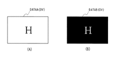
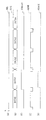
すなわち図34は、この面積階調方式の多ビットメモリ方式による画像表示装置を示すブロック図である。この画像表示装置1において、表示部2は、反射型液晶表示パネル又は透過型液晶表示パネルであり、赤色、緑色、青色のカラーフィルタを設けた画素がマトリックス状に配置して形成される。
In other words, FIG. 34 is a block diagram showing an image display apparatus based on the multi-bit memory method of the area gradation method. In the
ここで図35にこの表示部2の1つの画素2Aの構成を示すように、各画素2Aは、表示に供する部位である電極3A、3B、3C、3D、3E、3Fの面積が1:2:4:8:16:32に設定された複数のサブ画素2AA〜2AFにより形成される。ここで各サブ画素2AA〜2AFは、このような電極3A〜3Fの面積が一定の比例関係に設定される点を除いて同一に形成され、図36に示す画素回路4A〜4Fによりそれぞれ電極3A〜3Fによる液晶セル5A〜5Fを駆動する。
Here, as shown in FIG. 35, the configuration of one
すなわち画素回路4A〜4Fは、ゲート及びドレインがそれぞれ共通に接続されたNチャンネルMOS(以下、NMOSと呼ぶ)トランジスタQ1及びPチャンネルMOS(以下、PMOSと呼ぶ)トランジスタQ2からなるCMOSインバーター6と、同様に、ゲート及びドレインがそれぞれ共通に接続されたNMOSトランジスタQ3及びPMOSトランジスタQ4からなるCMOSインバーター7とが正側電源ラインVDDと負側電源ラインVSSとの間に並列に設けられ、これらCMOSインバーター6、7がループ状に接続されてSRAM(Static Random Access Memory )構成によるメモリが形成される。
That is, each of the
画素回路4A〜4Fは、NMOSトランジスタQ5によりこれらCMOSインバーター6、7に信号線SIGを接続して、信号線SIGの論理値をメモリに供給するスイッチ回路8が形成され、これにより図37に示すように、ゲート信号GATE(図37(B))によるNMOSトランジスタQ5の制御により、信号線SIG(図37(A))によるデータをメモリにセットする(図37(C))。なおここでV1は、このスイッチ回路8による入力側であるインバーター6の入力側の電位である。
In the
画素回路4A〜4Fは、このようにしてメモリに保持してなるデータに応じて、液晶セル5A(5B〜5F)の共通電極に印加される共通電圧VCOM(図37(G))に対して、同相の駆動信号FRP(図37(D))又は逆相の駆動信号XFRP(図37(E))を選択して液晶セル5A(5B〜5F)に印加し、これにより液晶セル5A(5B〜5F)を駆動する。すなわち画素回路4A〜4Fは、NMOSトランジスタQ6及びPMOSトランジスタQ7からなるスイッチ回路9をインバーター7の出力によりオンオフ制御し、このスイッチ回路9を介して共通電位VCOMと同相の駆動信号FRPを液晶セル5A(5B〜5F)に印加する。また同様のNMOSトランジスタQ8及びPMOSトランジスタQ9からなるスイッチ回路10をインバーター6の出力によりオンオフ制御し、このスイッチ回路10を介して共通電位VCOMと逆相の駆動信号XFRPを液晶セル5A(5B〜5F)に印加する。
The
これにより図37に示すように、信号線SIGの電位を切り換えた場合、続くゲート信号GATEの立ち上がりの時点t1より液晶セル5A(5B〜5F)に印加される電圧V5(図37(F))が共通電位VCOMに対して同相から逆相に切り換わり、液晶セル5A(5B〜5F)の表示、非表示を切り換えることができる。なおこの図37に示す例は、いわゆるノーマリーブラックによる場合である。
Thus, as shown in FIG. 37, when the potential of the signal line SIG is switched, the voltage V5 (FIG. 37 (F)) applied to the
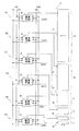
画像表示装置1において(図34)、インターフェース(IF)11は、各画素の階調を順次示すシリアルデータによる画像データSDI、この画像データSDIに同期したシステムクロックSCK、垂直同期信号に同期したタイミング信号SCSを、この画像表示装置1が設けられる機器の構成から入力する。インターフェース11は、この画像データSDIを表示部2の奇数ライン及び偶数ラインに対応する2系統に分離し、分離した画像データDATAをそれぞれ水平駆動部12O及び12Eに出力する。またこの画像データDATAに同期したクロックLSSCKを生成してタイミングジェネレータ14に出力する。またタイミング信号SCSにより、垂直同期信号に同期したタイミングで信号レベルが立ち上がるリセット信号RSTをタイミングジェネレータ14に出力する。
In the image display device 1 (FIG. 34), the interface (IF) 11 is configured to display image data SDI by serial data sequentially indicating the gradation of each pixel, a system clock SCK synchronized with the image data SDI, and timing synchronized with a vertical synchronization signal. The signal SCS is input from the configuration of the device in which the
タイミングジェネレータ14は、これらクロックLSSCK、リセット信号RSTより水平駆動部12O、12E、垂直駆動部15の動作に必要な各種タイミング信号を生成して出力する。
The
水平駆動部12O、12Eは、タイミングジェネレータ14から出力されるタイミング信号により動作し、それぞれ表示部2の奇数ライン及び偶数ラインの画素について、インターフェース11から出力される画像データDATAに対応するように信号線SIGの論理レベルを設定する。
The
すなわち図38に示すように、水平駆動部12O、12Eは、水平走査期間の開始のタイミングで立ち上がるタイミング信号HSTをシフトレジスタ(SR)21A、21B、……により順次ライン方向に転送して、各シフトレジスタ21A、21B、……から出力されるタイミング信号により画像データDATAをサンプリングラッチ(SL)22A、22B、……によりラッチする。これにより水平駆動部12O、12Eは、画像データDATAを対応する信号線SIGに振り分ける。
That is, as shown in FIG. 38, the
第2ラッチ23A、23B、……は、これらサンプリングラッチ22A、22B、……によるラッチ結果をそれぞれラッチして出力し、これにより各信号線SIGに振り分けた画像データのタイミングを一致させて出力する。パラレルシリアル変換回路(PS)24A、24B、……は、第2ラッチ23A、23B、……のラッチ結果Loutを構成する各ビットの論理値を、選択信号SERIにより順次選択して出力することにより、各信号線SIGに振り分けられた入力画像データをシリアルデータに変換して出力する。
The
すなわち図39及び図40に示すように、パラレルシリアル変換回路24A、24B、……において、アンド回路25〜30は、順次循環的に信号レベルが立ち上がる選択信号SERI0〜SERI5(図40(A0)〜(A5))により、それぞれラッチ結果Loutの各ビットの論理値Lout0〜Lout5をゲートし、オア回路31は、これらアンド回路25〜30の出力信号の論理和信号を生成する。パラレルシリアル変換回路24A、24B、……は、このオア回路31の出力信号をバッファ回路32を介して出力し、これにより各信号線SIGに振り分けた画像データを1ビットのシリアルデータにより各信号線SIG(図40(B))に出力する。
That is, as shown in FIGS. 39 and 40, in the parallel-
垂直駆動部15(図34)は、これら水平駆動部12O、12Eによる信号線SIGの駆動に対応するように、タイミングジェネレータ14で生成されたタイミング信号により表示部2の画素2Aをライン単位で選択し、かつ各ライン内では、サブ画素を順次選択するゲート信号GATE0〜GATE5に出力する。
The vertical drive unit 15 (FIG. 34) selects the
すなわち図41に示すように、垂直駆動部15は、垂直同期信号に同期して信号レベルが立ち上がるタイミング信号VST(図40(C))をシフトレジスタ(SR)41A、41B、……により順次垂直方向に転送する。垂直駆動部15は、アンド回路42A0〜42A5、42B0〜42B5、……により、順次循環的に信号レベルが立ち上がる選択信号ENB0〜ENB5(図40(D0)〜(D5))を、シフトレジスタ41A、41B、……の出力信号によりゲートして、各ラインの各サブ画素を順次選択するゲート信号GATE0〜GATE5(図40(E0)〜(E5))を生成し、このゲート信号GATE0〜GATE5をバッファ回路43A0〜43A5、43B0〜43B5、……を介して表示部2に出力する。
That is, as shown in FIG. 41, the
これらによりこの図34に示す例による画像表示装置1は、垂直方向の複数の画素に1つの信号線を時分割により振り分けて、さらには1つの画素を構成するサブ画素に時分割により1つの信号線SIGに振り分けて、各サブ画素の表示、非表示を制御して所望する画像を表示する。なおこのような多ビットメモリ方式による画像表示装置は、反射型液晶、透過型液晶に代えて、反射型電極と透過型電極とを併用した液晶セルを用いる場合にあっても、広く適用することができる。
Accordingly, the
しかしながらこの多ビットメモリ方式は、1つの画素を構成する複数のサブ画素間で電極を絶縁する必要があり、その分、表示に供しない無駄な領域が1つの画素に発生し、その結果として1つの画素における透過率、反射率が低下する欠点がある。これにより効率良く画像表示できない問題がある。 However, in this multi-bit memory system, it is necessary to insulate the electrodes between a plurality of sub-pixels constituting one pixel, and accordingly, a wasteful area not used for display is generated in one pixel. There is a drawback in that the transmittance and reflectance in one pixel are reduced. As a result, there is a problem that the image cannot be displayed efficiently.
また面積の異なるサブ画素をオンオフ制御して階調を表現していることにより、各画素の輝度に応じて各画素で表示に係る領域の重心の位置が変化し、これにより特定の階調でサブ画素の配置による固定パターンが見て取られる欠点がある。また最も面積の小さなサブ画素の加工精度により解像度、階調数が制限される欠点があり、さらには1つの画素に多くの半導体素子を設けることが必要になることにより、解像度、階調数が制限される欠点がある。これにより画質の点で実用上、未だ不十分な問題がある。
本発明は以上の点を考慮してなされたもので、多ビットメモリ方式において、これらの欠点を一挙に解決して、従来に比して効率良く高画質により画像表示することができる画像表示装置、電子機器、携帯機器及び画像表示方法を提案しようとするものである。 The present invention has been made in consideration of the above points, and in a multi-bit memory system, an image display apparatus capable of solving these drawbacks at once and displaying an image with high image quality more efficiently than in the past. An electronic device, a portable device, and an image display method are proposed.
かかる課題を解決するため請求項1の発明は、マトリックス状に画素を配置した表示部と、前記表示部にゲート信号を出力する垂直駆動部と、入力画像データを前記表示部の信号線に振り分けて出力する水平駆動部と、前記表示部、前記水平駆動部、垂直駆動部に動作基準用のタイミング信号を出力するタイミングジェネレータとを有する画像表示装置に適用して、前記入力画像データが多ビットの画像データであり、前記画素は、前記信号線に出力される前記入力画像データを、前記ゲート信号により選択的に入力して保持するメモリ部を有し、前記メモリ部に保持した前記入力画像データに応じた時分割の駆動により階調を表現する。
In order to solve such a problem, the invention of
また請求項14の発明は、画像取得手段で入力画像データを取得し、前記入力画像データを画像表示部により表示する電子機器に適用して、前記画像表示部は、マトリックス状に画素を配置した表示部と、前記表示部にゲート信号を出力する垂直駆動部と、前記入力画像データを前記表示部の信号線に振り分けて出力する水平駆動部と、前記表示部、前記水平駆動部、垂直駆動部に動作基準用のタイミング信号を出力するタイミングジェネレータとを有し、前記入力画像データが多ビットの画像データであり、前記画素は、前記信号線に出力される前記入力画像データを、前記ゲート信号により選択的に入力して保持するメモリ部を有し、前記メモリ部に保持した前記入力画像データに応じた時分割の駆動により階調を表現する。
Further, the invention of
また請求項15は、電池により動作し、画像取得手段で入力画像データを取得し、前記入力画像データを画像表示部により表示する携帯機器に適用して、前記画像表示部は、マトリックス状に画素を配置した表示部と、前記表示部にゲート信号を出力する垂直駆動部と、前記入力画像データを前記表示部の信号線に振り分けて出力する水平駆動部と、前記表示部、前記水平駆動部、垂直駆動部に動作基準用のタイミング信号を出力するタイミングジェネレータとを有し、前記入力画像データが多ビットの画像データであり、前記画素は、前記信号線に出力される前記入力画像データを、前記ゲート信号により選択的に入力して保持するメモリ部を有し、前記メモリ部に保持した前記入力画像データに応じた時分割の駆動により階調を表現する。 Further, the present invention is applied to a portable device that operates by a battery, acquires input image data by an image acquisition unit, and displays the input image data by an image display unit. , A vertical drive unit that outputs a gate signal to the display unit, a horizontal drive unit that distributes and outputs the input image data to signal lines of the display unit, the display unit, and the horizontal drive unit A timing generator that outputs a timing signal for operation reference to a vertical drive unit, the input image data is multi-bit image data, and the pixel outputs the input image data output to the signal line. A memory unit that selectively inputs and holds the gate signal and expresses gradation by time-division driving according to the input image data held in the memory unit
また請求項16の発明は、マトリックス状に配置した画素を対応する入力画像データにより駆動して、前記入力画像データによる画像を表示する画像表示方法に適用して、1つの画素に設けられた多ビットによるメモリ部に、対応する前記入力画像データを記録する画像データ記録のステップと、前記メモリ部の各ビットに応じた時間間隔による駆動により、前記入力画像データに応じた時分割の駆動により階調を表現する表示のステップとを有する。
The invention according to
請求項1の構成により、マトリックス状に画素を配置した表示部と、前記表示部にゲート信号を出力する垂直駆動部と、入力画像データを前記表示部の信号線に振り分けて出力する水平駆動部と、前記表示部、前記水平駆動部、垂直駆動部に動作基準用のタイミング信号を出力するタイミングジェネレータとを有する画像表示装置に適用して、前記入力画像データが多ビットの画像データであり、前記画素は、前記信号線に出力される前記入力画像データを、前記ゲート信号により選択的に入力して保持するメモリ部を有し、前記メモリ部に保持した前記入力画像データに応じた時分割の駆動により階調を表現すれば、多ビットメモリ方式により画像表示するようにして、面積階調法による場合に比して大面積の電極により画素を作成することができ、これにより電極間の無駄な領域を低減し、さらには固定パターンの発生を防止することができる。また電極の加工精度による解像度、階調数の制限も緩和され、さらには半導体素子数も少なくすることができ、これらにより多ビットメモリ方式において、従来に比して効率良く高画質により画像表示することができる。 2. A display unit having pixels arranged in a matrix, a vertical drive unit that outputs a gate signal to the display unit, and a horizontal drive unit that distributes input image data to signal lines of the display unit and outputs the divided signal. And applied to an image display device having a timing generator that outputs an operation reference timing signal to the display unit, the horizontal driving unit, and the vertical driving unit, and the input image data is multi-bit image data, The pixel includes a memory unit that selectively inputs and holds the input image data output to the signal line by the gate signal, and performs time division according to the input image data held in the memory unit If the gray scale is expressed by driving, the image is displayed by the multi-bit memory method, and the pixel is formed by the electrode having a large area as compared with the case of the area gray scale method. It can be, thereby reducing the wasted space between the electrodes, and further it is possible to prevent the occurrence of fixed pattern. In addition, the resolution and the number of gradations due to electrode processing accuracy are alleviated, and the number of semiconductor elements can be reduced. With these, in a multi-bit memory system, an image can be displayed with high image quality more efficiently than before. be able to.
これにより請求項14、請求項15、請求項16の構成によれば、多ビットメモリ方式において、従来に比して効率良く高画質により画像表示することができる。
Thus, according to the configurations of
本発明によれば、多ビットメモリ方式による画像表示において、従来の欠点を一挙に解決して、従来に比して効率良く高画質により画像表示することができる電子機器、携帯機器及び画像表示方法を提供することができる。 ADVANTAGE OF THE INVENTION According to this invention, in the image display by a multibit memory system, the conventional fault can be solved at a stretch, and an electronic device, a portable device, and an image display method capable of displaying an image with high image quality more efficiently than before. Can be provided.
以下、適宜図面を参照しながら本発明の実施例を詳述する。 Hereinafter, embodiments of the present invention will be described in detail with reference to the drawings as appropriate.
(1)実施例の構成
図2は、本発明の実施例1に係る画像表示装置を示すブロック図である。この画像表示装置51は、例えば図示しないチューナー部、外部機器等から出力されるビデオデータによる画像を、多ビットメモリ方式により表示部52で表示する。なおこの図2に示す画像表示装置51において、図34について上述した画像表示装置1と同一の構成は、対応する符号を付して示し、重複した説明は省略する。
(1) Configuration of Embodiment FIG. 2 is a block diagram showing an image display apparatus according to
ここで表示部52は、反射型液晶表示パネル又は透過型液晶表示パネルであり、赤色、緑色、青色のカラーフィルタを設けた画素がマトリックス状に配置して形成される。ここで図3にこの表示部52の1つの画素52Aの構成を示すように、画素52Aは、大面積による1つの電極53が表示に供する部位に配置され、この電極53を用いて液晶セルが形成される。また各画素52Aは、画素回路54が設けられ、この画素回路54による電極53の駆動により階調が表現される。
Here, the
ここで2ビットにより階調を表現する場合を例に取って画素回路54の構成を図1に示すように、各画素52Aは、図4に示すように、例えばフレーム周期により信号レベルが切り換わる共通電圧VCOM(図4(A))が各液晶セル55の共通電極に印加される。画素回路54は、ソース及びドレインがそれぞれ共通に接続されたNMOSトランジスタQ51及びPMOSトランジスタQ52からなるスイッチ回路56を介して、この共通電圧VCOMと同相の駆動信号FRP(図4(B))に電極53が接続され、また同様にソース及びドレインがそれぞれ共通に接続されたNMOSトランジスタQ53及びPMOSトランジスタQ54からなるスイッチ回路57を介して、共通電圧VCOMと逆相の駆動信号XFRP(図4(C))に電極53が接続される。
Here, taking as an example the case where gradation is expressed by 2 bits, the configuration of the
これにより画素回路54は、このスイッチ回路56、57を相補的にオンオフ制御して、液晶セル55の表示、非表示を切り換える。またさらに画素回路54は、それぞれ画像データの各ビットの表示を担当する駆動回路58A及び58Bにより時分割でこれらスイッチ回路56、57を相補的にオンオフ制御するようにして、これら駆動回路58A及び58Bによる時分割の駆動により階調を表現する。より具体的に、駆動回路58A及び58Bが担当する画像データのビットに対応するように、これら駆動回路58A及び58Bによるスイッチ回路56、57の駆動時間を設定し、これにより時分割により1つの電極53による液晶セル55を駆動する。
Accordingly, the
ここで駆動回路58A及び58Bは、担当するビット、制御に係る信号が異なる点を除いて同一に構成されることにより、以下においては、駆動回路58Aについてのみ構成を説明し、重複した説明は省略する。ここで駆動回路58Aは、ゲート及びドレインがそれぞれ共通に接続されたNMOSトランジスタQ56及びPMOSトランジスタQ57からなるCMOSインバーター60と、同様に、ゲート及びドレインがそれぞれ共通に接続されたNMOSトランジスタQ58及びPMOSトランジスタQ59からなるCMOSインバーター61とが正側電源ラインVDD1と負側電源ラインVSSとの間に並列に設けられ、これらCMOSインバーター60、61がループ状に接続されてSRAM構成によるメモリ62が形成される。
Here, the
さらにゲート信号GATEによりオンオフ動作して信号線SIGの論理値をこのメモリ62に書き込むNMOSトランジスタQ61によるスイッチ回路64が設けられ、選択信号SEPによりこのメモリ62の出力をスイッチ回路56、57に選択的に出力するNMOSトランジスタQ65、Q66によるスイッチ回路65、66が設けられる。これらによりこの画素回路54は、図5に示す等化回路により表すことができる。
Further, a
各画素回路54は、図4(D1)及び(D2)に示すように、各駆動回路58A、58Bに供給する選択信号SEP0、SEP1において、それぞれ信号レベルが立ち上がって駆動回路58A、58Bにそれぞれスイッチ回路56、57の制御を委ねる期間T0及びT1の比率が、入力画像データの各ビットに対応する比率に設定され、これによりこの図1の例ではこの期間T0及びT1の比率が1:2に設定される。なお信号線SIGからの論理値の入力は、図35を用いて各画素回路4A〜4Fについて説明した場合と同様にして、シリアルデータにより各駆動回路58A及び58Bに入力され、選択信号SEP0、SEP1によりスイッチ回路56、57の制御を委ねる期間が短い側の駆動回路58Aに画像データの下位側ビットの論理値が選択的に入力され、残りの駆動回路58Bに上位側ビットの論理値が選択的に入力される。
As shown in FIGS. 4D1 and 4D, each
これにより画素回路54は、駆動回路58A及び58Bのメモリ62により構成されるメモリ部に入力画像データを記録して保持し、このメモリ部に保持した入力画像データに応じた時分割の駆動により、時間軸方向の積分効果を利用して2ビットによる入力画像データの階調を表現する(図4(E))。
Thereby, the
このような階調表現原理により、画像表示装置51の画素52Aは(図3)、6ビットによる階調を表現できるように、6個の駆動回路58A〜58Fが設けられ、この6個の駆動回路58A〜58Fによるスイッチ回路56、57の制御時間が、選択信号SEP0〜SEP5により、各駆動回路58A〜58Fが表示を担当するビットに応じて設定される。
With such a gradation expression principle, the
すなわち画像表示装置51において(図2)、タイミングジェネレータ71は、図6に示すように、共通電圧VCOM、駆動信号FRP、XFRP(図6(A)〜(C))を生成して出力する。またスイッチ回路56、57の制御を各駆動回路58A〜58Fにそれぞれ委ねる選択信号SEP0〜SEP5(図6(D1)〜(D6))を、1フレームの期間の間で順次選択的に立ち上げるようにして、それぞれ選択信号SEP0〜SEP5の信号レベルが立ち上がっている期間T0〜T5が、下位側ビットから上位側ビットに向かうに従って2のべき乗で増大するように選択信号SEP0〜SEP5を生成する。これによりこの例では、最も下位側ビットに係る選択信号SEP0において、信号レベルが立ち上がっている期間T0に対して、これより上位側に係るSEP1〜SEP5は、信号レベルが立ち上がっている期間T1〜T5が、それぞれ2倍、4倍、8倍、16倍、32倍の期間に設定される(図6(E))。なおこの画像表示装置51は、これらのタイミングジェネレータ71、水平駆動部12O、12E等が表示部52のガラス基板上に一体に形成される。
That is, in the image display device 51 (FIG. 2), the
(2)実施例の動作
以上の構成において、この画像表示装置51は(図2)、インターフェース11を介して入力されるシリアルデータによる画像データSDIが、奇数ライン及び偶数ラインに分離されてそれぞれ水平駆動部12O及び12Eに入力され、ここで表示部52の各信号線SIGに振り分けられた後(図38)、1ビットによるシリアルデータに変換されて表示部52の各信号線SIGに出力される(図39)。またこの水平駆動部12O及び12Eによる信号線SIGの駆動に対応するように、垂直駆動部15によりゲート信号GATEが生成されて表示部52に供給され、これにより水平駆動部12O及び12Eより信号線SIGに出力された画像データが順次対応する画素に入力されて表示に供される。これによりこの画像表示装置51では、画像データSDIによる画像が表示部52で表示される。
(2) Operation of Embodiment In the above configuration, the image display device 51 (FIG. 2) is configured such that the image data SDI by serial data input via the
表示部52の各画素52Aにおいては(図1、図3及び図5)、対向電極が1つの大きな電極53により形成されて液晶セル55が形成され、スイッチ回路56、57の相補的なオンオフ制御により、この液晶セル55の共通電極に印加する共通電圧VCOMと同相の駆動信号FRPと、逆相の駆動信号XFRPとが選択的に電極53に印加される。これによりノーマリーブラックによる液晶セル55を構成する場合には、スイッチ回路56、57の制御により同相の駆動信号FRPを電極53に印加して画素52Aを非表示とすることができるのに対し、逆相の駆動信号XFRPを電極53に印加して表示状態とすることができる。
In each
この画像表示装置51は、ゲート信号GATE0〜GATE5による制御により、ビットシリアルにより信号線SIGに出力される画像データの論理値が、各ビット毎に、駆動回路58A〜58Fに設けられたメモリ62に順次書き込まれる。またこの書き込まれた論理値によりスイッチ回路56、57を制御するようにして、各駆動回路58A〜58Fにスイッチ回路56、57の制御を委ねる期間が、選択信号SEP0〜SEP5により、各駆動回路58A〜58Fが駆動を受け持つ画像データのビットに対応するように設定される。具体的に、上位階層を受け持つ駆動回路58A〜58Fになるに従って、2のべき乗により駆動を受け持つ期間が増大するように設定される。
In the
これによりこの画像表示装置51は、入力画像データを各画素52Aのメモリ部に記録し、このメモリ部に保持した入力画像データに応じた時分割の駆動により階調を表現する。
Thus, the
すなわち各画素52Aでは、これら駆動回路58A〜58Fの各メモリ62に記録された各ビットの論理値に応じて表示、非表示の期間が切り換えられ、人間の目の積分効果により、画像データSDIのビット数に対応する階調を表現することができる。これによりこの画像表示装置51は、多ビットメモリ方式により液晶セル55を駆動して、画像データSDIのビット数に対応する階調を表現することができ、水平駆動部12O、12E等にディジタルアナログ変換回路等を設ける必要が無い分、全体として簡易な構成により画像表示することができる。また必ずしもフレーム毎に画像データを書き込まなくてもよいこと等により、消費電力を低減することができる。
That is, in each
このようにして多ビットメモリ方式により画像表示するにつき、この画像表示装置51では、1つの電極53により1つの画素52Aを構成するようにして、この電極53の駆動を時分割により切り換えて階調を表現していることにより、図34について上述した面積階調方式による多ビットメモリ方式のような、サブ画素間の表示に供しない無駄な領域を省くことができ、その分、1つの画素における透過率、反射率の低下を防止して、効率良く画像表示することができる。
In this way, when an image is displayed by the multi-bit memory system, in this
また1つの電極53により1つの画素52Aを構成できることにより、面積階調方式による階調に応じた重心位置の変化を防止することができ、これにより固定パターンの発生を防止することができる。また最も面積の小さなサブ画素の加工精度による解像度、階調数の制限も回避することができる。さらに多ビットメモリ方式による場合のように、同相及び逆相の駆動信号の切り換えに係るスイッチ回路を、各ビット毎に設ける代わりに、各ビットに割り当てたメモリ62の出力を選択的にスイッチ回路56、57に出力するスイッチ回路を各ビットに割り当てれば良いことにより、その分、半導体素子数を少なくして全体構成を簡略化することができ、半導体素子数による解像度、階調数の制限も回避することができる。具体的には、各ビットで4個のトランジスタQ6〜Q9(図36)を省略し、代わりに全体としてスイッチ回路56、57を構成する4個のトランジスタQ51〜54と、各ビットに2個のトランジスタQ65、Q66を設ければ良いことになり、この実施例に係る6ビットによる階調の表現では、面積階調方式による多ビットメモリ方式では54個のトランジスタが必要であったところを、46個に低減することができる。
In addition, since one
これにより従来に比して効率良く高画質により画像表示することができる。 As a result, it is possible to display an image with high image quality more efficiently than in the past.
なおこれによりこの実施例に係る画像表示装置51では、液晶セルに印加する駆動信号のパルス幅の制御により階調を表現していることになり、このような手法による階調表現には、従来、STN(Super Twisted Nematic )液晶のパルス幅変調方式による階調表現方法がある。しかしながらこのSTN液晶のパルス幅変調方式は、アナログ方式による表示部の駆動であるのに対し、この実施例に係る駆動方式は、多ビットメモリ方式である点で根本的に相違していることになる。
As a result, in the
(3)実施例の効果
以上の構成によれば、入力画像データを各画素のメモリ部に記録し、このメモリ部に保持した入力画像データに応じた時分割の駆動により階調を表現することにより、多ビットメモリ方式による画像表示において、従来に比して効率良く高画質により画像表示することができる。
(3) Effects of the embodiment According to the above configuration, the input image data is recorded in the memory unit of each pixel, and the gradation is expressed by time-division driving according to the input image data held in the memory unit. Therefore, in the image display by the multi-bit memory system, it is possible to display the image with high image quality more efficiently than in the past.
より具体的に、入力画像データの各ビットの論理値をそれぞれ取得して記録する複数の1ビットのメモリを各画素に設け、この複数のメモリが担当する入力画像データのビット位置に応じた期間で、これら複数のメモリの記録をそれぞれ選択的にスイッチ回路により出力するようにして、このスイッチ回路の出力信号により、画素の電極に印加する信号を切り換えることにより、従来に比して簡易な構成により高画質の画像を表示することができる。 More specifically, each pixel is provided with a plurality of 1-bit memories for acquiring and recording the logical value of each bit of the input image data, and the period corresponding to the bit position of the input image data handled by the plurality of memories Thus, the recording of the plurality of memories is selectively output by the switch circuit, and the signal applied to the electrode of the pixel is switched by the output signal of the switch circuit. Thus, a high-quality image can be displayed.
また水平駆動部からビットシリアルによるシリアルデータにより入力画像データを信号線に出力するようにして、この入力画像データの各ビットの論理値を各画素でメモリに記録して表示に供することにより、信号線の配線数を低減して、表示部の構成を簡略化することができる。 In addition, the input image data is output to the signal line from the horizontal drive unit by serial data by bit serial, and the logical value of each bit of this input image data is recorded in the memory in each pixel and used for display. The number of lines can be reduced and the structure of the display portion can be simplified.
図7は、図3との対比により、本発明の実施例2に係る画像表示装置に適用される表示部の1画素を示す接続図である。この実施例に係る画像表示装置は、この画素82Aに係る電極83が透明電極と反射電極との併用により形成される。この実施例に係る画像表示装置は、この画素の構成が異なる点を除いて、実施例1の画像表示装置51と同一に構成される。
FIG. 7 is a connection diagram showing one pixel of the display unit applied to the image display apparatus according to the second embodiment of the present invention, in comparison with FIG. In the image display apparatus according to this embodiment, the
この実施例によれば、透明電極と反射電極との併用により液晶セルの電極を作成する場合でも、実施例1と同一の効果を得ることができる。 According to this embodiment, even when the electrode of the liquid crystal cell is formed by using the transparent electrode and the reflective electrode in combination, the same effect as that of the first embodiment can be obtained.
図8は、図3との対比により、本発明の実施例3に係る画像表示装置に適用される表示部の1画素を示す接続図である。この実施例3では、面積階調方法との組み合わせにより階調を表現する。このためこの実施例では、液晶セルの電極が複数のサブ電極により形成され、入力画像データの各ビットにおいて、表示に供するサブ電極の面積と駆動期間の長さとの乗算値が、それぞれビット位置に対応する2のべき乗比の関係となるように設定される。 FIG. 8 is a connection diagram showing one pixel of the display unit applied to the image display apparatus according to the third embodiment of the present invention, in comparison with FIG. In the third embodiment, gradation is expressed by a combination with the area gradation method. For this reason, in this embodiment, the electrodes of the liquid crystal cell are formed by a plurality of sub-electrodes, and in each bit of the input image data, the multiplication value of the area of the sub-electrode used for display and the length of the driving period is at the bit position. It is set to have a corresponding power-of-two ratio.
すなわち画素92Aは、画像データのビット数より少ない、3つのサブ電極93A、93B、93Cにより形成される。またこれら3つのサブ電極93A、93B、93Cは、面積が2のべき乗の関係に設定されて、面積比が1:2:4に設定される。
That is, the
また各サブ電極93A、93B、93Cには、それぞれ2ビットによる画素回路54A、54B、54Cが設けられ、各画素回路54A、54B、54Cでは、それぞれ駆動回路58A、58Bにスイッチ回路56、57の制御を委ねる期間の長さが1:8の関係に設定され、これに対応するようにタイミングジェネレータから選択信号SEP0、SEP1が供給される。
The sub-electrodes 93A, 93B, and 93C are each provided with
また最も面積の小さなサブ電極93Aから面積の大きい側のサブ電極93B及び93Cに、順次、入力画像データの最下位ビットから3ビットが割り当てられ、また続く上位側3ビットが順次割り当てられる。この実施例に係る画像表示装置は、これらの構成が異なる点を除いて、上述の実施例に係る画像表示装置と同一に構成される。
Further, 3 bits from the least significant bit of the input image data are sequentially assigned to the
この実施例によれば、面積階調方法との組み合わせにより階調を表現することにより、選択信号SEPの種類を少なくすることができ、その分、配線を簡略化してレイアウト効率を向上し、実施例1と同様の効果を得ることができる。また面積階調方式との組み合わせにより、画素設計の自由度を増大させることができる。 According to this embodiment, by expressing the gradation by combination with the area gradation method, the types of the selection signal SEP can be reduced, and accordingly, the wiring is simplified and the layout efficiency is improved. The same effect as in Example 1 can be obtained. Further, the combination with the area gradation method can increase the degree of freedom in pixel design.
図9は、図8との対比により、本発明の実施例4に係る画像表示装置に適用される表示部の1画素を示す接続図である。この実施例に係る画像表示装置は、この画素102Aに係るサブ電極103A、103B、103Cが透明電極と反射電極との併用により形成される。この実施例に係る画像表示装置は、この画素の構成が異なる点を除いて、上述の実施例に係る画像表示装置と同一に構成される。
FIG. 9 is a connection diagram showing one pixel of the display unit applied to the image display apparatus according to the fourth embodiment of the present invention, in comparison with FIG. In the image display apparatus according to this embodiment, the sub-electrodes 103A, 103B, and 103C related to the
この実施例によれば、透明電極と反射電極との併用により液晶セルの電極を作成する場合でも、実施例3と同一の効果を得ることができる。 According to this embodiment, even when the electrode of the liquid crystal cell is formed by using the transparent electrode and the reflective electrode in combination, the same effect as that of the embodiment 3 can be obtained.
図10〜図12は、実施例3、実施例4とは異なる他の例による面積階調方法との組み合わせによる階調表現方法を示す平面図である。面積階調方法との組み合わせによる階調表現は、入力画像データの各ビットにおいて、表示に供するサブ電極の面積と駆動期間の長さとの乗算値が、それぞれビット位置に対応する2のべき乗の関係となるように設定すれば良く、種々の組み合わせが考えられ、図10の例では、サブ電極の面積比を1:4:16に設定し、駆動期間の長さ比を1:2に設定した場合である。また図11は、サブ電極の面積比を1:8に設定し、駆動期間の長さ比を1:2:4に設定した場合であり、図12は、サブ電極の面積比を1:2に設定し、駆動期間の長さ比を1:4:8に設定した場合である。この実施例に係る画像表示装置は、これらの構成が異なる点を除いて、上述の実施例に係る画像表示装置と同一に構成される。 10 to 12 are plan views showing a gradation expression method by combination with an area gradation method according to another example different from the third and fourth embodiments. The gradation expression by the combination with the area gradation method is the relationship between the power of 2 corresponding to the bit position of the multiplication value of the area of the sub-electrode provided for display and the length of the driving period in each bit of the input image data. Various combinations are conceivable, and in the example of FIG. 10, the area ratio of the sub electrodes is set to 1: 4: 16, and the length ratio of the driving period is set to 1: 2. Is the case. FIG. 11 shows a case where the area ratio of the sub-electrode is set to 1: 8 and the length ratio of the driving period is set to 1: 2: 4. FIG. 12 shows the area ratio of the sub-electrode is 1: 2. This is a case where the length ratio of the driving period is set to 1: 4: 8. The image display apparatus according to this embodiment is configured in the same manner as the image display apparatus according to the above-described embodiment except that these configurations are different.
この実施例のように、サブ電極の面積比、駆動期間の長さ比を種々に変更するようにしても、実施例3、実施例4と同様の効果を得ることができる。 Even if the area ratio of the sub-electrode and the length ratio of the driving period are variously changed as in this embodiment, the same effects as those of the third and fourth embodiments can be obtained.
図13〜図15は、図5との対比により液晶セルの他の駆動回路の構成を示す接続図である。ここで液晶セルの時分割による駆動は、種々の構成を適用することができ、図13の例では、スイッチ回路57の駆動信号をインバーター110により反転してスイッチ回路56を駆動するようにして、駆動回路118A、118Bからの出力を1系統とし、スイッチ回路65を省略したものである。また図14は、スイッチ回路56の駆動信号をインバーター120により反転してスイッチ回路57を駆動するようにして、駆動回路128A、128Bからの出力を1系統とし、スイッチ回路66を省略したものである。また図15は、図14におけるスイッチ回路56、57、インバーター120をイクスクルーシブオア回路131に置き換え、併せて画素回路内で駆動信号FRPから駆動信号XFRPを生成するものである。この実施例に係る画像表示装置は、これらの構成が異なる点を除いて、上述の実施例に係る画像表示装置と同一に構成される。
13 to 15 are connection diagrams showing the configuration of another drive circuit of the liquid crystal cell in comparison with FIG. Here, various configurations can be applied to the time-division driving of the liquid crystal cell. In the example of FIG. 13, the drive signal of the
これらの実施例のように、液晶セルの駆動回路に種々の構成を適用しても、上述の実施例と同様の効果を得ることができる。 Even if various configurations are applied to the driving circuit of the liquid crystal cell as in these embodiments, the same effects as in the above-described embodiments can be obtained.
図16は、本発明の実施例7に係る画像表示装置に適用される表示部の構成を示す平面図である。この実施例に係る画像表示装置は、この表示部142に係る構成が異なる点を除いて、上述の実施例と同様に構成される。
FIG. 16 is a plan view showing a configuration of a display unit applied to an image display apparatus according to
ここでこの実施例では、液晶セルの時分割による駆動を制御する選択信号SEP0〜SEPN(SEP00〜SEPN0、SEP01〜SEPN1、SEP02〜SEPN2、……)の位相が、隣接するラインで異なるように設定し、これによりフリッカを防止する。なおここでこのライン毎に位相を異ならせる方法は、ライン毎に、選択信号SEP0〜SEPNの極性を反転させるようにしてもよく、また図17に示すように、ライン毎に一定位相づつ、選択信号SEP0〜SEPNの位相を順次シフトさせるようにしてもよく、これらを組み合わせるようにしてもよい。また連続するフレームの同一ラインで、これら選択信号SEP0〜SEPNの位相を異ならせるようにしてもよい。 Here, in this embodiment, the phases of the selection signals SEP0 to SEPN (SEP00 to SEPN0, SEP01 to SEPN1, SEP02 to SEPN2,...) For controlling the time-division driving of the liquid crystal cell are set to be different in adjacent lines. This prevents flicker. Here, as a method for making the phase different for each line, the polarity of the selection signals SEP0 to SEPN may be reversed for each line, and as shown in FIG. The phases of the signals SEP0 to SEPN may be sequentially shifted, or they may be combined. In addition, the phases of the selection signals SEP0 to SEPN may be varied on the same line of successive frames.
この実施例のように、液晶セルの時分割による駆動を制御する選択信号の位相を隣接するラインで異なるように設定することにより、フリッカを防止して、上述の実施例と同様の効果を得ることができる。 As in this embodiment, by setting the phase of the selection signal for controlling the time-division driving of the liquid crystal cell to be different between adjacent lines, flicker can be prevented and the same effect as the above-described embodiment can be obtained. be able to.
図18は、図2との対比により本発明の実施例8に係る画像表示装置を示すブロック図である。この画像表示装置181は、例えば携帯電話、電子スチルカメラ、ビデオカメラ等の携帯機器であり、ユーザーによる操作に応動して図示しないメモリに記録したプログラムを実行することにより全体の動作を制御するコントローラ184の制御により、表示部182の表示を切り換える。
FIG. 18 is a block diagram illustrating an image display apparatus according to an eighth embodiment of the present invention in comparison with FIG. The
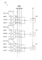
ここで表示部182は、図19に示すように、信号線SIGに出力される画像データを記録してスイッチ回路56、57を駆動する駆動回路58AA、58AB、……による第1の系統による駆動回路群186Aと、同様に、画像データを記録してスイッチ回路56、57を駆動する駆動回路58BA、58BB、……による第2の系統による駆動回路群186Bとの2系統により駆動回路が設けられ、これら2系統の駆動回路58AA、58AB、……、58BA、58BB、……の出力によりスイッチ回路56、57が制御される。
Here, as shown in FIG. 19, the
これに対応してタイミングジェネレータ183(図18)は、コントローラ184の制御により、これら2系統の駆動回路58AA、58AB、……、58BA、58BB、……に対応するように2系統による選択信号SEP0A〜SEP5A、SEP0B〜SEP5Bを選択的に出力し、これによりこれら2系統による駆動回路58AA、58AB、……、58BA、58BB、……で、スイッチ回路56、57の制御を切り換える。
In response to this, the timing generator 183 (FIG. 18), under the control of the
すなわちユーザーにより例えば撮像結果等による動画の表示が指示されると、図19に示すように、第1の系統に係る駆動回路58AA、58AB、……によりスイッチ回路56、57を制御するように選択信号SEP0A〜SEP5A、SEP0B〜SEP5Bを出力する。またユーザーにより電子メール等の表示が指示されると、図19との対比により図20に示すように、第2の系統の駆動回路58BA、58BB、……によりスイッチ回路56、57を制御するように選択信号SEP0A〜SEP5A、SEP0B〜SEP5Bを出力する。
That is, when the user instructs to display a moving image based on, for example, an imaging result, as shown in FIG. 19, selection is made to control the
またこれによりインターフェース(I/F)185は、コントローラ184の制御により、ビデオデータSDI、コントローラ184で生成された画像データDVからこれら2系統の駆動回路群186A、186Bに係る画像データDATAA、DATABを時分割により出力する。また垂直駆動部186は、同様のコントローラ184の制御により、この画像データDATAA、DATABの出力に対応するように、各系統のゲート信号GATEA、GATEBを出力する。
Accordingly, the interface (I / F) 185 controls the video data SDI and the image data DV generated by the
これに対してコントローラ184は、例えば各部の動作の監視により異常が検出されると、検出された異常をユーザーに警告する記号、メッセージ等を表示する画像データDVを生成する。またタイミングジェネレータ183の制御により、図21に示すように、これら2系統の駆動回路群186A及び186Bのうちの一方の系統に、この画像データDV(DATAA)を格納する。またこの画像データDVの階調を反転した画像データDVを生成し、残る他方の系統に、この階調を反転した画像データDV(DATAB)を格納する。またこのようにして各系統に画像データを格納すると、タイミングジェネレータ183の制御により選択信号SEPA、SEPBを複数フレーム周期で切り換えて出力し、これにより2系統の駆動回路による画像表示を複数フレーム周期により切り換え、この警告表示をブランキングにより表示する。
On the other hand, when an abnormality is detected, for example, by monitoring the operation of each unit, the
また図22に示すように、例えば電池残量が残り少なくなった場合、さらには記録媒体の空き容量が少なくなった場合には、これら2系統のうちの1系統でビデオデータSDIによる画像を表示するようにして、これらの状況をユーザーに警告する記号、メッセージ等を表示する画像データDVを生成し、残る1系統にこの画像データDVを格納する。なおこの画像データDVの格納にあっては、例えば1つ又は複数の垂直ブランキング期間で実行するようにしてもよく、さらには1フレームの期間だけ、ビデオデータSDIの書き込みを中止し、この中止した期間で実行するようにしてもよい。 Further, as shown in FIG. 22, for example, when the remaining battery level is low, or when the free capacity of the recording medium is low, an image based on the video data SDI is displayed in one of these two systems. In this way, image data DV for displaying symbols, messages, etc. for warning the user of these situations is generated, and this image data DV is stored in the remaining one system. The storage of the image data DV may be performed, for example, in one or more vertical blanking periods. Furthermore, the writing of the video data SDI is interrupted for only one frame period, and this cancellation is performed. You may make it perform in the period which carried out.
この場合、コントローラ184は、このようにして画像データDVを残る1系統に格納すると、フレーム周期によりこれら2系統で表示を切り換え、これにより動画による画像上に、この警告に係る文字、記号等をスーパーインポーズして表示する。
In this case, when the
この実施例によれば、各画素に、画像データを記録するメモリ部と、このメモリ部の記録により時分割に液晶セルを駆動する駆動部とを2系統設けることにより、これら2系統で表示を切り換えて種々の機能を確保するようにして、上述の実施例と同様の効果を得ることができる。 According to this embodiment, each pixel is provided with two systems of a memory unit that records image data and a drive unit that drives the liquid crystal cell in a time-sharing manner by recording in the memory unit, so that display can be performed with these two systems. By switching to ensure various functions, it is possible to obtain the same effects as in the above-described embodiment.
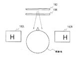
図23は、図18との対比により本発明の実施例9に係る画像表示装置を示すブロック図である。この画像表示装置191は、例えばモニタ装置であり、ビデオデータSDIを入力する。なおここでビデオデータSDIは、立体表示に供するビデオデータであり、右目用及び左目用の画像データがフレーム周期で交互に連続するビデオデータである。画像表示装置191は、このビデオデータSDIに係る構成が異なる点を除いて、実施例8について上述した画像表示装置181と同一に構成される。画像表示装置191は、この立体表示に供するビデオデータSDIの右目用及び左目用の画像データを表示部182に設けられた2系統の駆動回路群186A及び186Bにフレーム周期で交互に格納し、またフレーム周期でこの2系統の駆動回路群186A及び186Bに記録した画像データによる画像を表示部182で交互に表示する。
FIG. 23 is a block diagram showing an image display apparatus according to
この画像表示装置191は、この表示の切り換えに連動してコントローラ194により視差発生機構196の動作を制御し、これにより図24に示すように、右目用の表示画像182R及び左目用の表示画像182Lに視差を設けて、ビデオデータSDIによる右目用及び左目用の画像を視聴者に提供する。なおこのような視差発生機構196は、例えば光の偏向を利用した機構等、種々の機構を広く適用することができる。
The
この実施例では、画像データを記録するメモリ部と、このメモリ部の記録により時分割に液晶セルを駆動する駆動部とを2系統設けて、立体視に利用するようにして、上述の実施例と同様の効果を得ることができる。 In this embodiment, two systems of a memory section for recording image data and a drive section for driving the liquid crystal cell in a time-sharing manner by recording in the memory section are provided for stereoscopic viewing, and the above-described embodiment is used. The same effect can be obtained.
ここで上述した実施例では、各液晶セルの時分割による駆動がフレーム周期で実行されているものの、この駆動の周期を複数フレームに設定してもよい。このように複数フレーム周期により各液晶セルを時分割による駆動した場合、各信号線SIGへの画像データの出力に時間的な余裕が発生する。これによりこの実施例では、この時間的な余裕を有効に利用して、少ない駆動回路により多くの階調を表現する。 In the embodiment described above, although the time division driving of each liquid crystal cell is executed in a frame cycle, this driving cycle may be set to a plurality of frames. In this way, when each liquid crystal cell is driven in a time division manner with a plurality of frame periods, a time margin is generated in the output of image data to each signal line SIG. Thus, in this embodiment, the time margin is effectively used to express many gradations with a small number of drive circuits.
これによりこの実施例に係る画像表示装置は、表示部の画素が図1に示す2ビットの階調に対応するように構成されて、4ビットによる階調を表現する。なおこの実施例では、この表示部と、この表示部に関連する構成が異なる点を除いて、実施例1について上述した画像表示部と同一に構成されることにより、図2の構成を流用して構成を説明する。 Thus, the image display apparatus according to this embodiment is configured so that the pixels of the display unit correspond to the 2-bit gradation shown in FIG. 1, and expresses a 4-bit gradation. In this embodiment, except for the difference between the display unit and the configuration related to the display unit, the configuration shown in FIG. The configuration will be described.
ここで図25に示すように、この実施例において、水平駆動部12O及び12Eは、連続する3フレームのうちの先頭フレームで、4ビットによる画像データの最下位ビットB0、この最下位ビットB0から2ビットだけ上位のビットB2をビットシリアルにより信号線SIGに出力し、また続く2フレームで、残るビットB1及びB3をビットシリアルにより信号線SIGに出力する(図25(A))。
Here, as shown in FIG. 25, in this embodiment, the
タイミングジェネレータ71は、この先頭のフレームの期間を1:4の期間に分割し、続く2フレームの期間では、同様に、この2フレームの期間を1:4の期間に分割するように、選択信号SEP0、SEP1を出力する(図25(B)及び(C))。なおこの実施例では、この先頭フレームで出力した選択信号の繰り返しにより、続く2フレームの期間を1:4の期間に分割する。
The
表示部52は、これにより先頭フレームで信号線SIGに出力される入力画像データの各ビットB0及びB2をそれぞれ駆動回路58A、58Bに取得してスイッチ回路56、57の駆動に供する。また続く2フレームの期間で、信号線SIGに出力される入力画像データの各ビットB1及びB3をそれぞれ駆動回路58A、58Bに取得してスイッチ回路56、57の駆動に供する。
Accordingly, the
これによりこの実施例では、連続する3フレームにおける時分割駆動の繰り返しにより、各ビットB0〜B3の表示に供する期間を1:2:4:8の関係に設定して所望する画像を表示する。 Thus, in this embodiment, by repeating time-division driving in three consecutive frames, a desired image is displayed by setting the period used for displaying each bit B0 to B3 to a relationship of 1: 2: 4: 8.
この実施例のように、複数フレームによる繰り返しにより、入力画像データに応じて時分割で駆動することにより、全体の構成を一段と簡略化することができる。 As in this embodiment, the entire configuration can be further simplified by driving in time division according to input image data by repeating a plurality of frames.
図26は、図2との対比により本発明の実施例11に係る画像表示装置を示すブロック図である。この画像表示装置201は、例えば携帯電話等の電池により動作する携帯機器に適用されて、高い階調が必要な場合には、アナログ信号による駆動により表示部202で画像を表示する。これに対して例えば電子メールのようなテキスト表示等の高い階調が不要な場合、さらには待ち受け画面の表示のように、常時、電力消費の表示の場合、ビット数の少ない多ビットメモリ方式により表示部202で画像表示する。このためこの画像表示装置201は、この駆動方式の切り換えに対応するように表示部202等が構成される。なおこの実施例において、上述の実施例と同一の構成は、対応する符号を付して示し、重複した説明は省略する。
FIG. 26 is a block diagram showing an image display apparatus according to Example 11 of the present invention in comparison with FIG. The
ここで図27は、この表示部202の1つの画素の構成を示す接続図である。この画素202Aは、図1について上述した2ビットによる多ビットメモリ方式による構成に加えて、アナログ信号による駆動に供する構成が設けられる。すなわちこの画素202Aは、2ビットによる画素回路54Aによるスイッチ回路56、57の出力が、NMOSトランジスタQ200によるディジタル駆動切り換え用のスイッチ回路203を介して液晶セル55に出力される。
Here, FIG. 27 is a connection diagram showing the configuration of one pixel of the
この液晶セル55は、保持容量CS1が設けられ、アナログ駆動切り換え用のゲート信号AGATEによりオンオフ動作するNMOSトランジスタQ201によるスイッチ回路204を介して、信号線SIGに接続される。これによりこの画素202Aは、アナログ駆動切り換え用のスイッチ回路204、ディジタル駆動切り換え用のスイッチ回路203をそれぞれオフ状態、オン状態に設定して、多ビットメモリ方式による時分割駆動により液晶セル55を駆動する。またこれとは逆に、アナログ駆動切り換え用のスイッチ回路204、ディジタル駆動切り換え用のスイッチ回路203をそれぞれオン状態、オフ状態に設定して、信号線SIGに出力される駆動信号の信号レベルに応じた階調により液晶セル55を駆動する。
The
水平駆動部206O、206Eは、それぞれ表示部202の奇数ライン及び偶数ラインの信号線SIGに、アナログ信号駆動に係る駆動信号、入力画像データを選択的に出力する。すなわち図28に示すように、水平駆動部206O、206Eは、水平走査期間の開始のタイミングで立ち上がるタイミング信号HSTをシフトレジスタ(SR)21A、21B、……により順次ライン方向に転送して、各シフトレジスタ21A、21B、……から出力されるタイミング信号によりサンプリングラッチ(SL)22A、22B、……により画像データDATAをラッチし、これにより画像データDATAを対応する信号線SIGに振り分ける。
The
また第2ラッチ23A、23B、……によるこれらサンプリングラッチ22A、22B、……によるラッチ結果をそれぞれラッチして出力し、これにより各信号線SIGに振り分けた画像データのタイミングを一致させ、パラレルシリアル変換回路(PS)210A、210B、……は、タイミングジェネレータ205から出力されるタイミング信号SERIにより、第2ラッチ23A、23B、……から出力される6ビットによる画像データの下位側2ビットを選択的に取得してシリアルデータに変換する。
Further, the latch results obtained by the sampling latches 22A, 22B,... By the
水平駆動部206O、206Eは、さらにディジタルアナログ変換回路(DAC)211A、211B、……により第2ラッチ23A、23B、……から出力される6ビットによる画像データをディジタルアナログ変換処理してアナログ信号駆動に係る駆動信号を出力する。
The
水平駆動部206O、206Eは、タイミングジェネレータ205から出力される選択信号SEL、XSELにより相補的にオンオフ動作するスイッチ回路213A及び214A、213B及び214B、……を介して、パラレルシリアル変換回路210A、210B、……の出力データ、ディジタルアナログ変換回路211A、211B、……に出力されるアナログ信号駆動に係る駆動信号を選択的に信号線SIGに出力する。
The
図29に示すように、垂直駆動部207は、垂直同期信号に同期して信号レベルが立ち上がるタイミング信号VSTをシフトレジスタ(SR)41A、41B、……により順次垂直方向に転送する。垂直駆動部207は、それぞれアンド回路211A〜21Cにおいて、タイミングジェネレータ205から出力されるアナログ信号駆動の選択信号AENB、多ビットメモリ方式の駆動においてそれぞれ下位側ビット及び上位側ビットの書き込みを指示する選択信号DENB0、DENB1を、シフトレジスタ41A、41B、……の出力信号によりゲートし、これによりアナログ信号駆動、多ビットメモリ方式の駆動の各ビットを選択するゲート信号AGATE、DGATE0、DGATE1を生成し、このゲート信号AGATE、DGATE0、DGATE1をそれぞれバッファ回路212A〜212Cを介して表示部202に出力する。
As shown in FIG. 29, the
これらによりこの画像表示装置201では、図30に示すように、選択信号レベルSEL(図30(A))をHレベルに設定した状態で、タイミング信号SERI、SER0(図30(B)及び(C))に同期して第2ラッチ23A、23B、・でラッチされる画像データの2ビットLou0、Lou0が交互に信号線SIG(図30(D))に出力される。また垂直駆動部207からそれぞれ下位側ビット及び上位側ビットの書き込みを指示する選択信号DEMB0、DEMB1(図30(F)及び(G))が、シフトレジスタ41Aから出力されるタイミング信号VSRout(図30(E))によりゲートされて、ゲート信号DGATE1、DGATE2(図30(H)及び(L))が出力され、このゲート信号DGATE1、DGATE2によりそれぞれ駆動回路58A及び58Bに、信号線SIGに出力された画像データの各ビットが記録され、この記録により液晶セル55が駆動される。
Accordingly, in the
これに対して図31に示すように、選択信号レベルSEL(図31(A))をLレベルに設定した状態で、ディジタルアナログ変換回路211A、211B、・による駆動信号が信号線SIGに出力され(図31(B))、アナログ信号駆動を選択する選択信号SENB(図31(D))がシフトレジスタ41Aから出力されるタイミング信号VSRout(図31(C))によりゲートされて、ゲート信号AGATE(図31(E))が出力され、ゲート信号AGATEにより信号線SIGに出力される駆動信号で液晶セル55が駆動される。
On the other hand, as shown in FIG. 31, in the state where the selection signal level SEL (FIG. 31A) is set to the L level, the drive signals from the digital /
なお図32は、図30及び図31との対比により、時点t1で、多ビットメモリ方式による駆動から、アナログ信号駆動に駆動を切り換えた場合を示すタイムチャートである。 FIG. 32 is a time chart showing a case where the driving is switched from the driving by the multi-bit memory system to the analog signal driving at the time point t1 in comparison with FIGS. 30 and 31.
これによりタイミングジェネレータ205は、コントローラ208の制御により、水平駆動部206O、206E、垂直駆動部207、表示部202に、これらの動作に必要な各種のタイミング信号を生成して出力する。
As a result, the
コントローラ208は、ユーザーによる操作に応動して図示しないメモリに記録したプログラムを実行することにより全体の動作を制御する制御手段であり、ユーザーが撮像結果の取得を指示すると、図示しない撮像部の動作を制御して撮像結果を取得する。コントローラ208は、この撮像結果による動画、静止画によるビデオデータSDIをインターフェース11に入力し、またアナログ信号駆動により動作するようにタイミングジェネレータ205の動作を制御する。また図示しないメモリにこの撮像結果を記録して保持し、この記録して保持した撮像結果の表示がユーザーにより指示されると、同様にしてこの撮像結果を表示部202で表示する。これによりコントローラ208は、高い階調による表示が必要な場合には、アナログ信号による駆動により表示部202で画像を表示するように全体の動作を制御する。
The
これに対して待ち受け画面表示、電子メールの表示では、多ビットメモリ方式により表示するようにタイミングジェネレータ205の動作を切り換え、これにより消費電力を低減する。
On the other hand, in the standby screen display and e-mail display, the operation of the
この実施例によれば、別途、アナログ信号駆動の構成を設けて表示を切り換えることにより、消費電力の低減を図りつつ、高画質により画像表示するようにして、実施例1と同様の効果を得ることができる。 According to this embodiment, separately, by switching the display provided in the analog signal driving structure, while reducing the power consumption, so as to display images by image quality, the same effect as in Example 1 be able to.
図33は、本発明の実施例12に係る画像表示装置の表示画面を示す平面図である。この実施例に係る画像表示装置は、携帯電話に適用されて、実施例11について説明した画像表示装置201の構成において、コントローラ208によるタイミングジェネレータ205の制御により、表示画面を縦方向に2つの領域ARA、ARBに分割し、このうちの画面上部側の領域ARAをパーシャル表示領域に設定する。
FIG. 33 is a plan view showing a display screen of the image display apparatus according to
ここでパーシャル表示領域は、この機器の状況を常時通知することが必要な情報の表示領域であり、例えば電池の残量、電界強度等の情報が表示される。 Here, the partial display area is a display area for information that needs to be constantly notified of the status of the device, and displays information such as the remaining battery level and electric field strength.
この実施例で、コントローラ208は、このパーシャル表示領域ARAを上述の多ビットメモリ方式により表示するようにタイミングジェネレータ205の動作を設定する。また表示中の情報の更新が必要になった場合にだけ、この多ビットメモリ方式に係る駆動回路に記録した画像データを更新し、その分消費電力を低減する。
In this embodiment, the
これに対して残りの領域ARBでは、アナログ信号駆動により画像表示する。 On the other hand, in the remaining area ARB, an image is displayed by analog signal driving.
この実施例によれば、表示画面の一部で多ビットメモリ方式により画像表示して、残りをアナログ信号駆動による画像表示することにより、消費電力を低減して、実施例11と同様の効果を得ることができる。なおこの場合、この領域による表示方式の切り換えに対応するように、表示部の構成をそれぞれ各領域に専用な構成とするようにしてもよい。
According to this embodiment, an image is displayed by a multi-bit memory system on a part of the display screen, and the remaining image is displayed by analog signal driving, thereby reducing power consumption and achieving the same effect as the
なお上述の実施例においては、多ビットメモリ方式により、2ビット又は6ビットの入力画像データを表示する場合について述べたが、本発明はこれに限らず、種々のビット数による画像データを表示する場合にも広く適用することができる。 In the above-described embodiments, the case where 2-bit or 6-bit input image data is displayed by the multi-bit memory method has been described. However, the present invention is not limited to this, and image data with various bit numbers is displayed. It can be widely applied to cases.
また上述の実施例においては、SRAMの構成により各駆動回路にメモリを設ける場合について述べたが、本発明はこれに限らず、例えばDRAMによるメモリを適用する場合等、種々の構成を広く適用することができる。 In the above-described embodiments, the case where the memory is provided in each drive circuit by the configuration of the SRAM has been described. However, the present invention is not limited to this, and various configurations are widely applied, for example, when a memory using a DRAM is applied. be able to.
また上述の実施例においては、各6ビットの赤色、緑色、青色の色データによる入力画像データを入力して画像表示する場合について述べたが、本発明はこれに限らず、4種類以上の色データによりカラー画像を表示する場合等にも広く適用することができる。 In the above-described embodiment, the case has been described in which image data is displayed by inputting input image data of 6-bit red, green, and blue color data. However, the present invention is not limited to this, and four or more colors are used. The present invention can be widely applied to a case where a color image is displayed using data.
また上述の実施例においては、ガラス基板上に表示部等を作成してなる液晶表示装置に本発明を適用する場合について述べたが、本発明はこれに限らず、EL(Electro Luminescence)表示装置等、種々の表示装置に広く適用することができる。 In the above-described embodiments, the case where the present invention is applied to a liquid crystal display device in which a display unit or the like is formed on a glass substrate has been described. However, the present invention is not limited to this, and an EL (Electro Luminescence) display device. The present invention can be widely applied to various display devices.
本発明は、例えば多ビットメモリ方式による液晶表示装置に適用することができる。 The present invention can be applied to, for example, a liquid crystal display device using a multi-bit memory system.
1、51、181、191、201……画像表示装置、2、52、142、182、202……表示部、2A、52A、82A、102A、202A……画素、3A〜3F、53、83……電極、4A〜4F、54、54A、54B、54C……画素回路、5A、55……液晶セル、6、7、60、61、110、120……インバーター、8〜10、56〜59、64〜66、203、204、213A、214A、213B、214B……スイッチ回路、11、120……インターフェース、12O、12E、206O、206E……水平駆動部、14、71、183、205……タイミングジェネレータ、15、186、207……垂直駆動部、21A、21B、41A、41B……シフトレジスタ、22A、22B……サンプリングラッチ、23A、23B……第2ラッチ、24A、24B、210A、210B……パラレルシリアル変換回路、31、184、194……コントローラ、58A、58B、58AA、58AB、58BA、58BB、186A及び186B……駆動回路、62……メモリ、93A〜93C、103A〜103C……サブ電極、211A、211B……ディジタルアナログ変換回路、Q1〜Q66……トランジスタ
DESCRIPTION OF
Claims (15)
前記画素は、
前記入力画像データを保持するメモリ部と、
前記入力画像データのビット数に比して数が少なく、表示に供する部位の面積が異なる複数のサブ画素とを有し、
前記メモリ部に保持した前記入力画像データの対応するビットの論理値に応じた前記サブ画素の時分割の駆動により、前記入力画像データに応じた階調を表現し、
前記メモリ部は、
前記入力画像データの各ビットのデータをそれぞれ保持する複数ビットのメモリと、
前記入力画像データにおける前記各ビットの位置に応じた期間で、前記各ビットのデータを選択的に出力するメモリ出力用のスイッチ回路とを有し、
前記画素は、
前記メモリ出力用のスイッチ回路の出力信号により、前記画素の電極に印加する信号を、前記画素の共通電極に印加される電圧と同相の駆動信号と逆相の駆動信号とを択一的に選択して印加することによって切り換える駆動信号切り換え用のスイッチ回路を有する
画像表示装置。 A display unit having pixels arranged in a matrix; a vertical drive unit that outputs a gate signal to the display unit; and a horizontal drive unit that outputs multi-bit input image data to a signal line of the display unit. ,
The pixel is
A memory unit for holding the input image data;
A plurality of sub-pixels having a smaller number of bits than the number of bits of the input image data and different areas of the portions used for display;
By representing the time division driving of the sub-pixel according to the logical value of the corresponding bit of the input image data held in the memory unit, to express the gradation according to the input image data ,
The memory unit is
A multi-bit memory for holding each bit of the input image data; and
A switch circuit for memory output that selectively outputs the data of each bit in a period according to the position of each bit in the input image data;
The pixel is
A signal applied to the electrode of the pixel is alternatively selected from a drive signal having the same phase as the voltage applied to the common electrode of the pixel and a drive signal having a phase opposite to that applied to the common electrode of the pixel, based on an output signal of the switch circuit for memory output. An image display device having a switch circuit for switching a drive signal that is switched by application .
前記少なくとも2つのビットのデータの各々は、前記同一の期間において、前記表示に供する部位が異なる複数のサブ画素の各々に出力される
請求項1に記載の画像表示装置。 The period corresponding to the position of each bit is the same period in at least two bits,
2. The image display device according to claim 1 , wherein each of the at least two bits of data is output to each of a plurality of sub-pixels having different parts for display in the same period .
前記入力画像データをシリアルデータにより対応する信号線に出力し、
前記垂直駆動部は、
前記シリアルデータに同期して順次信号レベルが立ち上がる複数のゲート信号を出力し、
前記画素は、
前記複数のゲート信号により、前記シリアルデータの各ビットの論理値を順次取得して前記メモリ部に記録する
請求項1に記載の画像表示装置。 The horizontal drive unit is
The input image data is output to the corresponding signal line by serial data,
The vertical driving unit includes:
A plurality of gate signals whose signal levels rise sequentially in synchronization with the serial data are output,
The pixel is
The image display device according to claim 1 , wherein a logical value of each bit of the serial data is sequentially acquired by the plurality of gate signals and recorded in the memory unit .
隣接するライン間で、前記時分割の駆動に係る位相が異なる
請求項1に記載の画像表示装置。 The pixel is
The image display device according to claim 1 , wherein phases related to the time-division driving are different between adjacent lines .
前記メモリ部を複数系統有し、
前記時分割の駆動に供する入力画像データを、前記複数系統で切り換える
請求項1に記載の画像表示装置。 The pixel is
A plurality of memory units;
The image display device according to claim 1 , wherein input image data used for the time-division driving is switched between the plurality of systems .
請求項5に記載の画像表示装置。 The image display device according to claim 5 , wherein the image display by switching between the plurality of systems is an image display by superimposition .
請求項1に記載の画像表示装置。 The image display device according to claim 1 , wherein the time-division driving is a display in which a period of one frame is repeated .
請求項1に記載の画像表示装置。 The image display apparatus according to claim 1, wherein the time-division driving is a display in which a period of the plurality of frames is divided into a plurality of frames and the driving by each bit of the input image data is repeated.
前記入力画像データをディジタルアナログ変換処理してアナログ信号を出力するディジタルアナログ変換部と、
選択信号に応じて、前記入力画像データに代えて、前記アナログ信号を前記信号線に出力する選択回路とを有し、
前記画素は、
選択信号に応じて、前記時分割による駆動に代えて、前記信号線に出力されるアナログ信号により駆動して階調を表現する
請求項1に記載の画像表示装置。 The horizontal drive unit is
A digital-to-analog conversion unit that performs digital-to-analog conversion processing on the input image data and outputs an analog signal;
In accordance with a selection signal, a selection circuit that outputs the analog signal to the signal line instead of the input image data,
The pixel is
The image display apparatus according to claim 1 , wherein gray scales are expressed by driving with an analog signal output to the signal line instead of the time-division driving in accordance with a selection signal .
前記選択信号に応じて、前記時分割による駆動を停止する動作停止用のスイッチ回路と、
前記信号線に出力されるアナログ信号を選択的に入力するアナログ信号用のスイッチ回路とを有する
請求項10に記載の画像表示装置。 The pixel is
In response to the selection signal, an operation stop switch circuit for stopping the driving by the time division,
The image display device according to claim 10 , further comprising: an analog signal switch circuit that selectively inputs an analog signal output to the signal line .
前記入力画像データをディジタルアナログ変換処理してアナログ信号を出力するディジタルアナログ変換部と、
選択信号に応じて、前記入力画像データに代えて、前記アナログ信号を前記信号線に出力する選択回路とを有し、
前記表示部の一部領域の画素は、
選択信号に応じて、前記時分割による駆動に代えて、前記信号線に出力されるアナログ信号により駆動して階調を表現する
請求項1に記載の画像表示装置。 The horizontal drive unit is
A digital-to-analog conversion unit that performs digital-to-analog conversion processing on the input image data and outputs an analog signal;
In accordance with a selection signal, a selection circuit that outputs the analog signal to the signal line instead of the input image data,
Pixels in a partial area of the display unit are
Depending on the selection signal, instead of driving by the time division, an image display apparatus according to claim 1 for expressing a gray scale by driving by an analog signal output to the signal line.
前記画像表示部は、
マトリックス状に画素を配置した表示部と、前記表示部にゲート信号を出力する垂直駆動部と、多ビットの入力画像データを前記表示部の信号線に出力する水平駆動部とを有しており、
前記画素は、
前記入力画像データを保持するメモリ部と、
前記入力画像データのビット数に比して数が少なく、表示に供する部位の面積が異なる複数のサブ画素とを有し、
前記メモリ部に保持した前記入力画像データの対応するビットの論理値に応じた前記サブ画素の時分割の駆動により、前記入力画像データに応じた階調を表現し、
前記メモリ部は、
前記入力画像データの各ビットのデータをそれぞれ保持する複数ビットのメモリと、
前記入力画像データにおける前記各ビットの位置に応じた期間で、前記各ビットのデータを選択的に出力するメモリ出力用のスイッチ回路とを有し、
前記画素は、
前記メモリ出力用のスイッチ回路の出力信号により、前記画素の電極に印加する信号を、前記画素の共通電極に印加される電圧と同相の駆動信号と逆相の駆動信号とを択一的に選択して印加することによって切り換える駆動信号切り換え用のスイッチ回路を有する
電子機器。 Multi-bit input image data is acquired by an image acquisition means, the input image data is displayed by an image display unit,
The image display unit
A display unit having pixels arranged in a matrix; a vertical drive unit that outputs a gate signal to the display unit; and a horizontal drive unit that outputs multi-bit input image data to a signal line of the display unit. ,
The pixel is
A memory unit for holding the input image data;
A plurality of sub-pixels having a smaller number of bits than the number of bits of the input image data and different areas of the portions used for display;
By representing the time division driving of the sub-pixel according to the logical value of the corresponding bit of the input image data held in the memory unit, to express the gradation according to the input image data,
The memory unit is
A multi-bit memory for holding each bit of the input image data; and
A switch circuit for memory output that selectively outputs the data of each bit in a period according to the position of each bit in the input image data;
The pixel is
A signal applied to the electrode of the pixel is alternatively selected from a drive signal having the same phase as the voltage applied to the common electrode of the pixel and a drive signal having a phase opposite to that applied to the common electrode of the pixel, based on an output signal of the switch circuit for memory output. An electronic apparatus having a switch circuit for switching a drive signal that is switched by applying the same .
前記画像表示部は、
マトリックス状に画素を配置した表示部と、前記表示部にゲート信号を出力する垂直駆動部と、多ビットの入力画像データを前記表示部の信号線に出力する水平駆動部とを有しており、
前記画素は、
前記入力画像データを保持するメモリ部と、
前記入力画像データのビット数に比して数が少なく、表示に供する部位の面積が異なる複数のサブ画素とを有し、
前記メモリ部に保持した前記入力画像データの対応するビットの論理値に応じた前記サブ画素の時分割の駆動により、前記入力画像データに応じた階調を表現し、
前記メモリ部は、
前記入力画像データの各ビットのデータをそれぞれ保持する複数ビットのメモリと、
前記入力画像データにおける前記各ビットの位置に応じた期間で、前記各ビットのデータを選択的に出力するメモリ出力用のスイッチ回路とを有し、
前記画素は、
前記メモリ出力用のスイッチ回路の出力信号により、前記画素の電極に印加する信号を、前記画素の共通電極に印加される電圧と同相の駆動信号と逆相の駆動信号とを択一的に選択して印加することによって切り換える駆動信号切り換え用のスイッチ回路を有する
携帯機器。 Operated by a battery , multi-bit input image data is acquired by an image acquisition means, the input image data is displayed by an image display unit,
The image display unit
A display unit having pixels arranged in a matrix; a vertical drive unit that outputs a gate signal to the display unit; and a horizontal drive unit that outputs multi-bit input image data to a signal line of the display unit. ,
The pixel is
A memory unit for holding the input image data;
A plurality of sub-pixels having a smaller number of bits than the number of bits of the input image data and different areas of the portions used for display;
By representing the time division driving of the sub-pixel according to the logical value of the corresponding bit of the input image data held in the memory unit, to express the gradation according to the input image data ,
The memory unit is
A multi-bit memory for holding each bit of the input image data; and
A switch circuit for memory output that selectively outputs the data of each bit in a period according to the position of each bit in the input image data;
The pixel is
A signal applied to the electrode of the pixel is alternatively selected from a drive signal having the same phase as the voltage applied to the common electrode of the pixel and a drive signal having a phase opposite to that applied to the common electrode of the pixel, based on an output signal of the switch circuit for memory output. A portable device having a switch circuit for switching a drive signal that is switched when applied .
前記画素は、
前記入力画像データを保持するメモリ部と、
前記入力画像データのビット数に比して数が少なく、表示に供する部位の面積が異なる複数のサブ画素とを有し、
前記メモリ部は、
前記入力画像データの各ビットのデータをそれぞれ保持する複数ビットのメモリと、
前記入力画像データにおける前記各ビットの位置に応じた期間で、前記各ビットのデータを選択的に出力するメモリ出力用のスイッチ回路とを有する
画像表示装置における画像表示に当たって、
前記メモリ部に保持した前記入力画像データの対応するビットの論理値に応じた前記サブ画素の時分割の駆動により、前記入力画像データに応じた階調を表現し、
前記メモリ出力用のスイッチ回路の出力信号により、前記画素の電極に印加する信号を、前記画素の共通電極に印加される電圧と同相の駆動信号と逆相の駆動信号とを択一的に選択して印加することによって切り換える
画像表示方法。 It comprises a display unit pixels arranged in a Matrix form, a vertical driver that outputs a gate signal to the display unit, and a horizontal driving unit for outputting an input image data of the multi-bit signal line of the display unit And
The pixel is
A memory unit for holding the input image data;
A plurality of sub-pixels having a smaller number of bits than the number of bits of the input image data and different areas of the portions used for display ;
The memory unit is
A multi-bit memory for holding each bit of the input image data; and
A memory output switch circuit that selectively outputs the data of each bit in a period corresponding to the position of each bit in the input image data.
In image display in the image display device,
By representing the time division driving of the sub-pixel according to the logical value of the corresponding bit of the input image data held in the memory unit, to express the gradation according to the input image data ,
A signal applied to the electrode of the pixel is alternatively selected from a drive signal having the same phase as the voltage applied to the common electrode of the pixel and a drive signal having a phase opposite to that applied to the common electrode of the pixel, based on an output signal of the switch circuit for memory output. The image display method is switched by applying the image.
Priority Applications (7)
| Application Number | Priority Date | Filing Date | Title |
|---|---|---|---|
| JP2005341410A JP5121136B2 (en) | 2005-11-28 | 2005-11-28 | Image display device, electronic device, portable device, and image display method |
| US12/083,992 US8599176B2 (en) | 2005-11-28 | 2006-11-02 | Image display device, electronic apparatus, portable apparatus, and image displaying method |
| KR1020087012654A KR101330486B1 (en) | 2005-11-28 | 2006-11-02 | Image display apparatus, electronic device, portable terminal device, and method of displaying image |
| PCT/JP2006/322423 WO2007060842A1 (en) | 2005-11-28 | 2006-11-02 | Image display apparatus, electronic device, portable terminal device, and method of displaying image |
| CN2006800444650A CN101317211B (en) | 2005-11-28 | 2006-11-02 | Image display apparatus, electronic device, portable terminal device, and method of displaying image |
| EP06832476A EP1956581A4 (en) | 2005-11-28 | 2006-11-02 | Image display apparatus, electronic device, portable terminal device, and method of displaying image |
| TW095141011A TWI423201B (en) | 2005-11-28 | 2006-11-06 | An image display device, an electronic device, a portable machine, and an image display method |
Applications Claiming Priority (1)
| Application Number | Priority Date | Filing Date | Title |
|---|---|---|---|
| JP2005341410A JP5121136B2 (en) | 2005-11-28 | 2005-11-28 | Image display device, electronic device, portable device, and image display method |
Related Child Applications (1)
| Application Number | Title | Priority Date | Filing Date |
|---|---|---|---|
| JP2011152428A Division JP2011215635A (en) | 2011-07-11 | 2011-07-11 | Image display device, electronic apparatus, mobile apparatus, and image display method |
Publications (3)
| Publication Number | Publication Date |
|---|---|
| JP2007147932A JP2007147932A (en) | 2007-06-14 |
| JP2007147932A5 JP2007147932A5 (en) | 2009-01-08 |
| JP5121136B2 true JP5121136B2 (en) | 2013-01-16 |
Family
ID=38067074
Family Applications (1)
| Application Number | Title | Priority Date | Filing Date |
|---|---|---|---|
| JP2005341410A Expired - Fee Related JP5121136B2 (en) | 2005-11-28 | 2005-11-28 | Image display device, electronic device, portable device, and image display method |
Country Status (7)
| Country | Link |
|---|---|
| US (1) | US8599176B2 (en) |
| EP (1) | EP1956581A4 (en) |
| JP (1) | JP5121136B2 (en) |
| KR (1) | KR101330486B1 (en) |
| CN (1) | CN101317211B (en) |
| TW (1) | TWI423201B (en) |
| WO (1) | WO2007060842A1 (en) |
Cited By (1)
| Publication number | Priority date | Publication date | Assignee | Title |
|---|---|---|---|---|
| US11862079B2 (en) * | 2021-12-07 | 2024-01-02 | Lg Display Co., Ltd. | Display device |
Families Citing this family (23)
| Publication number | Priority date | Publication date | Assignee | Title |
|---|---|---|---|---|
| JP4816686B2 (en) | 2008-06-06 | 2011-11-16 | ソニー株式会社 | Scan driver circuit |
| JP4693009B2 (en) * | 2008-10-07 | 2011-06-01 | 奇美電子股▲ふん▼有限公司 | Active matrix display device and portable device including the same |
| KR101746198B1 (en) | 2009-09-04 | 2017-06-12 | 가부시키가이샤 한도오따이 에네루기 켄큐쇼 | Display device and electronic device |
| US20110157322A1 (en) | 2009-12-31 | 2011-06-30 | Broadcom Corporation | Controlling a pixel array to support an adaptable light manipulator |
| KR20120017648A (en) * | 2010-08-19 | 2012-02-29 | 삼성전자주식회사 | Display apparatus and driving method of display panel |
| TWI423239B (en) * | 2010-09-14 | 2014-01-11 | Orise Technology Co Ltd | Integrated circuit for sram standby power reduction in lcd driver |
| JP5687110B2 (en) * | 2011-03-29 | 2015-03-18 | 株式会社ジャパンディスプレイ | Display device |
| JP2013057853A (en) * | 2011-09-09 | 2013-03-28 | Japan Display West Co Ltd | Display device, driving method of display device, and electronic apparatus |
| JP5879902B2 (en) * | 2011-10-13 | 2016-03-08 | セイコーエプソン株式会社 | Electro-optical device and electronic apparatus |
| JP6111588B2 (en) * | 2011-11-30 | 2017-04-12 | 株式会社Jvcケンウッド | Liquid crystal display device and driving method thereof |
| JP5923343B2 (en) | 2012-03-01 | 2016-05-24 | 株式会社ジャパンディスプレイ | Display device, driving method of display device, and electronic apparatus |
| JP5801734B2 (en) | 2012-03-01 | 2015-10-28 | 株式会社ジャパンディスプレイ | Liquid crystal display device, driving method of liquid crystal display device, and electronic apparatus |
| JP5865134B2 (en) * | 2012-03-15 | 2016-02-17 | 株式会社ジャパンディスプレイ | Liquid crystal display device, driving method of liquid crystal display device, and electronic apparatus |
| CN102930849A (en) * | 2012-11-05 | 2013-02-13 | 黑龙江省电力有限公司信息通信分公司 | Displayer for pushing overlapping display content by serial communication interface |
| JP6506961B2 (en) | 2013-12-27 | 2019-04-24 | 株式会社半導体エネルギー研究所 | Liquid crystal display |
| CA2873476A1 (en) * | 2014-12-08 | 2016-06-08 | Ignis Innovation Inc. | Smart-pixel display architecture |
| CN106169288B (en) * | 2016-08-30 | 2018-01-12 | 武汉华星光电技术有限公司 | Display driver circuit and dot structure |
| JP6846272B2 (en) | 2017-04-19 | 2021-03-24 | 株式会社ジャパンディスプレイ | Display device |
| JP6978971B2 (en) * | 2017-06-29 | 2021-12-08 | 株式会社ジャパンディスプレイ | Display device |
| CN110021260B (en) * | 2018-06-27 | 2021-01-26 | 京东方科技集团股份有限公司 | Pixel circuit, driving method thereof and display device |
| CN112017597B (en) * | 2019-05-29 | 2021-10-12 | 成都辰显光电有限公司 | Pixel circuit and display device |
| KR102156270B1 (en) * | 2020-04-02 | 2020-09-15 | 주식회사 사피엔반도체 | Sub-pixel driving circuit capable of operating in a low-quality mode and a high-definition mode using the same pixel memory and a display device including the same |
| JP7133051B2 (en) * | 2021-02-26 | 2022-09-07 | 株式会社ジャパンディスプレイ | Display device |
Family Cites Families (28)
| Publication number | Priority date | Publication date | Assignee | Title |
|---|---|---|---|---|
| JPS6064395A (en) * | 1983-09-20 | 1985-04-12 | セイコーエプソン株式会社 | Integrated circuit substrate for active panel |
| JP3485229B2 (en) * | 1995-11-30 | 2004-01-13 | 株式会社東芝 | Display device |
| US5945972A (en) * | 1995-11-30 | 1999-08-31 | Kabushiki Kaisha Toshiba | Display device |
| JP3292093B2 (en) * | 1997-06-10 | 2002-06-17 | 株式会社日立製作所 | Liquid crystal display |
| JP2000206922A (en) * | 1999-01-14 | 2000-07-28 | Sharp Corp | Display device |
| TW573165B (en) | 1999-12-24 | 2004-01-21 | Sanyo Electric Co | Display device |
| KR100758622B1 (en) | 2000-01-14 | 2007-09-13 | 마쯔시다덴기산교 가부시키가이샤 | Active matrix display apparatus and method for driving the same |
| JP2002175039A (en) * | 2000-01-14 | 2002-06-21 | Matsushita Electric Ind Co Ltd | Active matrix display and drive method therefor |
| US7180496B2 (en) * | 2000-08-18 | 2007-02-20 | Semiconductor Energy Laboratory Co., Ltd. | Liquid crystal display device and method of driving the same |
| JP4954400B2 (en) | 2000-08-18 | 2012-06-13 | 株式会社半導体エネルギー研究所 | Semiconductor device |
| JP2002156953A (en) | 2000-09-05 | 2002-05-31 | Toshiba Corp | Display device and its driving method |
| US6965365B2 (en) * | 2000-09-05 | 2005-11-15 | Kabushiki Kaisha Toshiba | Display apparatus and driving method thereof |
| JP3664059B2 (en) * | 2000-09-06 | 2005-06-22 | セイコーエプソン株式会社 | Electro-optical device driving method, driving circuit, electro-optical device, and electronic apparatus |
| TW507192B (en) * | 2000-09-18 | 2002-10-21 | Sanyo Electric Co | Display device |
| JP3711006B2 (en) * | 2000-09-18 | 2005-10-26 | 三洋電機株式会社 | Display device |
| KR100823047B1 (en) * | 2000-10-02 | 2008-04-18 | 가부시키가이샤 한도오따이 에네루기 켄큐쇼 | Self light emitting device and driving method thereof |
| JP3705123B2 (en) * | 2000-12-05 | 2005-10-12 | セイコーエプソン株式会社 | Electro-optical device, gradation display method, and electronic apparatus |
| JP3618687B2 (en) * | 2001-01-10 | 2005-02-09 | シャープ株式会社 | Display device |
| JP2002287718A (en) | 2001-01-18 | 2002-10-04 | Sharp Corp | Display device, portable appliance and substrate |
| JP2002268600A (en) * | 2001-03-13 | 2002-09-20 | Ricoh Co Ltd | Method for assigning intensity levels, display controller and display device |
| US7009590B2 (en) * | 2001-05-15 | 2006-03-07 | Sharp Kabushiki Kaisha | Display apparatus and display method |
| JP3767737B2 (en) | 2001-10-25 | 2006-04-19 | シャープ株式会社 | Display element and gradation driving method thereof |
| JP2003177717A (en) * | 2001-12-07 | 2003-06-27 | Sharp Corp | Display device |
| KR20030083123A (en) | 2002-04-19 | 2003-10-30 | 삼성전자주식회사 | Flat panel display and driving method thereof |
| JP2004086154A (en) | 2002-06-28 | 2004-03-18 | Seiko Epson Corp | Method for driving electrooptical device, electrooptical device, and electronic apparatus |
| JP4595296B2 (en) * | 2002-09-18 | 2010-12-08 | セイコーエプソン株式会社 | ELECTRO-OPTICAL DEVICE, ELECTRONIC DEVICE, AND PROJECTOR |
| JP2005164814A (en) * | 2003-12-01 | 2005-06-23 | Sony Corp | Display device and method for driving the same |
| JP4524699B2 (en) * | 2007-10-17 | 2010-08-18 | ソニー株式会社 | Display device |
-
2005
- 2005-11-28 JP JP2005341410A patent/JP5121136B2/en not_active Expired - Fee Related
-
2006
- 2006-11-02 KR KR1020087012654A patent/KR101330486B1/en active IP Right Grant
- 2006-11-02 WO PCT/JP2006/322423 patent/WO2007060842A1/en active Application Filing
- 2006-11-02 EP EP06832476A patent/EP1956581A4/en not_active Ceased
- 2006-11-02 US US12/083,992 patent/US8599176B2/en active Active
- 2006-11-02 CN CN2006800444650A patent/CN101317211B/en not_active Expired - Fee Related
- 2006-11-06 TW TW095141011A patent/TWI423201B/en not_active IP Right Cessation
Cited By (1)
| Publication number | Priority date | Publication date | Assignee | Title |
|---|---|---|---|---|
| US11862079B2 (en) * | 2021-12-07 | 2024-01-02 | Lg Display Co., Ltd. | Display device |
Also Published As
| Publication number | Publication date |
|---|---|
| TWI423201B (en) | 2014-01-11 |
| US20090091579A1 (en) | 2009-04-09 |
| US8599176B2 (en) | 2013-12-03 |
| KR20080070045A (en) | 2008-07-29 |
| CN101317211A (en) | 2008-12-03 |
| EP1956581A1 (en) | 2008-08-13 |
| KR101330486B1 (en) | 2013-11-15 |
| JP2007147932A (en) | 2007-06-14 |
| CN101317211B (en) | 2011-08-10 |
| EP1956581A4 (en) | 2010-06-23 |
| WO2007060842A1 (en) | 2007-05-31 |
| TW200731192A (en) | 2007-08-16 |
Similar Documents
| Publication | Publication Date | Title |
|---|---|---|
| JP5121136B2 (en) | Image display device, electronic device, portable device, and image display method | |
| JP5046226B2 (en) | Image display device | |
| US20130063499A1 (en) | Display device, driving method of display device, and electronic apparatus | |
| US9495897B2 (en) | Display device, method of driving display device, and electronic appliance | |
| WO2011092944A1 (en) | Multi-primary color display device | |
| JP2016071320A (en) | Display device and method associated with display device | |
| JP2009175468A (en) | Display | |
| TWI514843B (en) | Electro-optical device and electronic apparatus | |
| US9728121B2 (en) | Organic el display panel with color shutter glass unit selecting a monochromatic, a color, a monochromatic three-dimensional and a color three-dimensional display mode | |
| JP2006171034A (en) | Display apparatus and mobile terminal | |
| JP2011215635A (en) | Image display device, electronic apparatus, mobile apparatus, and image display method | |
| CN110751924A (en) | Micro-LED display screen controlled in split screen mode | |
| JPH02267591A (en) | System and device for multicolor display | |
| JP2005164814A (en) | Display device and method for driving the same | |
| JP5079777B2 (en) | Liquid crystal display | |
| JP2005309304A (en) | Data line driving circuit, electro-optical device, and electronic equipment | |
| JP2018017787A (en) | Electro-optic device, method for controlling the same, and electronic apparatus | |
| JP4556411B2 (en) | Electro-optic device | |
| JP4367211B2 (en) | Electro-optical device, driving method of electro-optical device, and electronic apparatus | |
| JP5703768B2 (en) | Electro-optical device and electronic apparatus | |
| WO2015137428A1 (en) | Liquid crystal driving device and liquid crystal display device | |
| JP2013109130A (en) | Electro-optical device, electronic apparatus and control method | |
| JPH02213894A (en) | Color matrix display device | |
| KR20060019753A (en) | Light emitting display and driving method thereof | |
| JP2004341217A (en) | Liquid crystal driving device |
Legal Events
| Date | Code | Title | Description |
|---|---|---|---|
| A521 | Request for written amendment filed |
Free format text: JAPANESE INTERMEDIATE CODE: A523 Effective date: 20081117 |
|
| A621 | Written request for application examination |
Free format text: JAPANESE INTERMEDIATE CODE: A621 Effective date: 20081117 |
|
| A521 | Request for written amendment filed |
Free format text: JAPANESE INTERMEDIATE CODE: A821 Effective date: 20090326 |
|
| RD02 | Notification of acceptance of power of attorney |
Free format text: JAPANESE INTERMEDIATE CODE: A7422 Effective date: 20090326 |
|
| RD04 | Notification of resignation of power of attorney |
Free format text: JAPANESE INTERMEDIATE CODE: A7424 Effective date: 20090402 |
|
| A131 | Notification of reasons for refusal |
Free format text: JAPANESE INTERMEDIATE CODE: A131 Effective date: 20110517 |
|
| A521 | Request for written amendment filed |
Free format text: JAPANESE INTERMEDIATE CODE: A523 Effective date: 20110708 |
|
| A131 | Notification of reasons for refusal |
Free format text: JAPANESE INTERMEDIATE CODE: A131 Effective date: 20111115 |
|
| A521 | Request for written amendment filed |
Free format text: JAPANESE INTERMEDIATE CODE: A523 Effective date: 20111226 |
|
| A711 | Notification of change in applicant |
Free format text: JAPANESE INTERMEDIATE CODE: A711 Effective date: 20120330 |
|
| TRDD | Decision of grant or rejection written | ||
| A01 | Written decision to grant a patent or to grant a registration (utility model) |
Free format text: JAPANESE INTERMEDIATE CODE: A01 Effective date: 20121002 |
|
| A01 | Written decision to grant a patent or to grant a registration (utility model) |
Free format text: JAPANESE INTERMEDIATE CODE: A01 |
|
| A61 | First payment of annual fees (during grant procedure) |
Free format text: JAPANESE INTERMEDIATE CODE: A61 Effective date: 20121023 |
|
| FPAY | Renewal fee payment (event date is renewal date of database) |
Free format text: PAYMENT UNTIL: 20151102 Year of fee payment: 3 |
|
| R150 | Certificate of patent or registration of utility model |
Free format text: JAPANESE INTERMEDIATE CODE: R150 Ref document number: 5121136 Country of ref document: JP Free format text: JAPANESE INTERMEDIATE CODE: R150 |
|
| R250 | Receipt of annual fees |
Free format text: JAPANESE INTERMEDIATE CODE: R250 |
|
| R250 | Receipt of annual fees |
Free format text: JAPANESE INTERMEDIATE CODE: R250 |
|
| R250 | Receipt of annual fees |
Free format text: JAPANESE INTERMEDIATE CODE: R250 |
|
| R250 | Receipt of annual fees |
Free format text: JAPANESE INTERMEDIATE CODE: R250 |
|
| LAPS | Cancellation because of no payment of annual fees |