Background technology
Traditionally, at LCD, openly so-called area has been proposed than gray level system among the No.2005-1641814 etc. in early days at Japanese patent application.In this system, a pixel is made of a plurality of sub-pixels with different area, and changes the area in the zone that is used to show by the demonstration/control that does not show to these a plurality of sub-pixels, thereby changes the gray level of each pixel.In addition, this Japanese patent application discloses No.2005-1641814 in early days and has proposed a kind of method, this method provides one storer for each sub-pixel, and by in this storer, writing down the demonstration of controlling corresponding sub-pixel/do not show, thereby the gray level of the input image datas that expression is made of a plurality of positions.Hereinafter, such system will be called as the multi-bit memory system, and in this system, each pixel is provided with multi-bit memory, and by in this multi-bit memory, writing down the gray level of representing each pixel.
Fig. 1 shows based on the block diagram of area than the image display device of the multi-bit memory system of gray level system.In this image display device 1, display unit 2 is reflective liquid crystal display panel or transmission-type liquid crystal display panel, and forms by arranging the pixel that is provided with the red, green, blue color filter with the form of matrix.
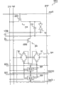
Fig. 2 shows the configuration of a pixel 2A in this display unit 2.As shown in Figure 2, each pixel 2A is made of to 2AF a plurality of sub-pixel 2AA, and wherein the area ratio as electrode 3A, 3B, 3C, 3D, 3E and the 3F of the parts that are used to show was set as 1: 2: 4: 8: 16: 32.Each sub-pixel 2AA is formed to 2AF has identical configuration, and just electrode 3A is designed to have certain proportionate relationship to the area of 3F.In these sub-pixels, comprise that electrode 3A is driven to 4F by image element circuit 4A respectively to 5F to the liquid crystal cells 5A of 3F, as shown in Figure 3.
Particularly, image element circuit 4A comprises CMOS phase inverter 6 and CMOS phase inverter 7 to 4F.CMOS phase inverter 6 is made of N-channel MOS (hereinafter, being called as NMOS) transistor Q1 and P channel MOS (hereinafter, being called as PMOS) transistor Q2, and these two transistorized grids and drain electrode are connected to each other.CMOS phase inverter 7 is made of nmos pass transistor Q3 and PMOS transistor Q4, and these two transistorized grids and drain electrode also are connected to each other similarly. CMOS phase inverter 6 and 7 is set between positive polarity power lead VDD and the negative polarity power lead VSS in parallel with each other, and is connected to each other with the form of loop, thereby has formed the storer based on SRAM (static random-access memory) configuration.In 4F, nmos pass transistor Q5 is as on-off circuit 8 at image element circuit 4A, and this on-off circuit 8 is connected to CMOS phase inverter 6 and 7 and the logical value of signal wire SIG offered storer with signal wire SIG.Based on this configuration, as shown in Figure 4, by utilizing the control of gate-control signal GATE (Fig. 4 (B)) pair nmos transistor Q5, the data of process signal wire SIG (Fig. 4 (A)) are set at (Fig. 4 (C)) in the storer.Symbol V1 represents the input side electromotive force of phase inverter 6, and phase inverter 6 is positioned at input side for this on-off circuit 8.
At image element circuit 4A in 4F, according to the data that are stored in the storer, respectively with common electric voltage VCOM (Fig. 4 (the G)) homophase of the public electrode that is applied to liquid crystal cells 5A (5B is to 5F) and anti-phase drive signal FRP (Fig. 4 (D)) and drive signal XFRP (Fig. 4 (E)) in one selected and be applied to liquid crystal cells 5A (5B is to 5F), thereby drive liquid crystal cells 5A (5B is to 5F).In other words, image element circuit 4A utilizes the output of phase inverter 7 to control the ON/OFF of the on-off circuit 9 that is made of nmos pass transistor Q6 and PMOS transistor Q7 to 4F, thereby will be applied to liquid crystal cells 5A (5B is to 5F) via this on-off circuit 9 with the drive signal XFRP of common potential VCOM homophase.In addition, the ON/OFF of the on-off circuit 10 that image element circuit 4A utilizes phase inverter 6 to 4F output control is made of similar nmos pass transistor Q8 and PMOS transistor Q9, thus will be applied to liquid crystal cells 5A (5B is to 5F) via this on-off circuit 10 with the anti-phase drive signal FRP of common potential VCOM.Because these operations, as shown in Figure 4, if the electromotive force of signal wire SIG is switched, then be applied to timing t 1 place of the gate-control signal GATE rising of voltage V5 (Fig. 4 (F)) after the electromotive force of signal wire SIG switches of liquid crystal cells 5A (5B is to 5F), switch to anti-phase with it voltage from voltage with common potential VCOM homophase.This makes that the state of liquid crystal cells 5A (5B is to 5F) can be at show state and do not switch between the show state.Example shown in Fig. 4 is corresponding to the situation of so-called normal black pattern.
In image display device 1 (Fig. 1), interface (IF) 11 is according to the configuration of the equipment that is provided with this image display device 1, input as the view data SDI of the serial data of the gray level of sequentially indicating each pixel, with synchronous system clock SCK of this view data SDI and the timing signal SCS synchronous with vertical synchronizing signal.Interface 11 is divided into odd-numbered line and the corresponding binary channels data of even number line with display unit 2 with this view data SDI, and the view data DATA after separated is outputed to horizontal driver 12O and 12E.In addition, interface 11 produces and the synchronous clock LSSCK of this view data DATA, and it is outputed to timing generator 14.In addition, based on timing signal SCS, interface 11 is to timing generator 14 output reset signal RST, and the signal level of this signal is in the timing place rising synchronous with vertical synchronizing signal.
Timing generator 14 produces necessary various timing signals of operation for horizontal driver 12O and 12E and vertical driver 15 according to clock LSSCK and reset signal RST, and the signal that produced of output.
Horizontal driver 12O and 12E are according to operating from the timing signal of timing generator 14 outputs, and at the odd-numbered line of display unit 2 and the pixel on the even number line, and from the view data DATA of the interface 11 output logic level of signalization line SIG matchingly.
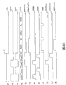
Particularly, as shown in Figure 5, in horizontal driver 12O and 12E, the timing signal HST that timing place that begins in the horizontal scanning period is risen follow direction sequentially by shift register (SR) 21A, 21B ... be transmitted, and view data DATA according to from corresponding shift register 21A, 21B ... the timing signal of output, by sample latch (SL) 22A, 22B ... latch.This makes horizontal driver 12O and 12E view data DATA can be distributed to corresponding signal lines SIG.
The second latch 23A, 23B ... latch and export sample latch 22A, 22B ... latch result.This can distribute to the view data of each signal wire SIG in identical timing place output.And-string change-over circuit (PS) 24A, 24B ... according to select signal SERI sequentially select and export the second latch 23A, 23B ... latch result Lout in the logical value of corresponding positions, thereby the input image data that will be assigned to corresponding signal lines SIG is converted to serial data and with its output.
Particularly, as shown in Fig. 6 and 7, also-string change-over circuit 24A, 24B ... in, AND circuit 25 to 30 sequentially circulates the selection signal SERI0 that rises to SERI5 (Fig. 7 (A0) arrives Fig. 7 (A5)) based on signal level, and the logical value Lout0 that comes the corresponding positions among the gating latch result Lout is to Lout5.The OR signal that OR circuit 31 produces from the output signal of these AND circuit 25 to 30.And-string change-over circuit 24A, 24B ... via the output signal of buffer circuit 32 outputs from this OR circuit 31, thereby the view data that will be assigned to each signal wire SIG outputs to signal wire SIG as bit serial data (Fig. 7 (B)).
With these horizontal drivers 12O and 12E to the driving of signal wire SIG matchingly, vertical driver 15 (Fig. 1) is selected pixel 2A in the display unit 2 line by line according to the timing signal that is produced by timing generator 14.In addition, at each row, vertical driver 15 output gate-control signal GATE0 are to GATE5, with chooser pixel sequentially.
Particularly, as shown in Figure 8, in vertical driver 15, the timing signal VST (Fig. 7 (C)) that its signal level and vertical synchronizing signal rise synchronously vertically by shift register (SR) 41A, 41B ... be transmitted.In vertical driver 15, AND circuit 42A0 to 42A5,42B0 to 42B5 ... based on from shift register 41A, 41B ... its signal level of output signal gating sequentially circulate the selection signal ENB0 that rises to ENB5 (Fig. 7 (D0) is to 7 (D5)), thereby produce gate-control signal GATE0 to GATE5 (Fig. 7 (E0) is to 7 (E5)), be used for sequentially selecting each of sub-pixel on the corresponding line.Vertical driver 15 with gate-control signal GATE0 to GATE5 via buffer circuit 43A0 to 43A5,43B0 to 43B5 ... output to display unit 2.
Based on above-mentioned configuration, in the image display device 1 of the example shown in Fig. 1, one signal line is assigned to vertically a plurality of pixels of arranging based on time division mechanism, and a signal line SIG is assigned to a plurality of sub-pixels in the pixel based on time division mechanism.Control by to the demonstration of each sub-pixel/do not show shows desired image.Image display device based on this multi-bit memory system can be widely used, even can be applied to replace reflective liquid crystal or transmission-type liquid crystal and use under the situation of the liquid crystal cells that adopts reflecting electrode and two kinds of electrodes of transmission electrode.
Yet this multi-bit memory system need make the electrode of a plurality of sub-pixels in the pixel insulated from each other.This can produce the useless region that has no to contribute for the demonstration in the pixel, can cause the transmissivity of a pixel and the shortcoming that reflectivity reduces.This has just caused the problem that can't realize that the high-level efficiency image shows.
In addition because gray level is to represent by the open/close control to sub-pixel with different area, so with the center that shows relevant zone can be according to the brightness of pixel and along with different pixels changes.This can produce following shortcoming: at specific gray level place, the fixed pattern of the arrangement of sub-pixel can visually occur depending on.In addition, have following shortcoming: the resolution of gray level and number are subjected to having the restriction of processing accuracy of the sub-pixel of minimum area.In addition, also there is following shortcoming: need in a pixel, a large amount of semiconductor elements be set, thereby and limit the resolution and the quantity of gray level.Owing to these reasons, said system exists picture quality can not satisfy the problem of practical application.
Embodiment
Describe embodiments of the invention below with reference to the accompanying drawings in detail.
The configuration of (1) first embodiment
Fig. 9 is the block diagram that illustrates according to the image display device of the first embodiment of the present invention.This image display device 51 utilizes the multi-bit memory system, comes display image based on for example video data from tuner unit or unshowned external unit output on display unit 52.For the image display device shown in Fig. 9 51, the assembly identical with those assemblies in the above image display device 1 described in conjunction with Figure 1 is endowed identical symbol, and omitted being repeated in this description about them.
Display unit 52 is reflective liquid crystal display panel or transmission-type liquid crystal display panel, and forms by arranging the pixel that is provided with the red, green, blue color filter with matrix form.Figure 10 shows the configuration of a pixel 52A in this display unit 52.As shown in Figure 10, in pixel 52A, have a large-area electrode 53 and be set at the part that is used to show, and utilize this electrode 53 to form liquid crystal cells.Each pixel 52A is provided with image element circuit 54, and by utilizing 54 pairs of electrodes 53 of this image element circuit to drive the representing gradation level.
Figure 11 illustrates and utilizes two ios dhcp sample configuration IOS DHCPs that come the corresponding image element circuit 54 of situation of representing gradation level.As shown in Figure 12, in each pixel 52A, common electric voltage VCOM (Figure 12 (A)) is applied to the public electrode of liquid crystal cells 55, and the signal level of described common electric voltage VCOM for example is to be switched in the cycle with the frame.In image element circuit 54, electrode 53 is connected to drive signal FRP (Figure 12 (B)) with this common electric voltage VCOM homophase via on-off circuit 56, described on-off circuit 56 is made of nmos pass transistor Q51 and PMOS transistor Q52, and these two transistorized source electrodes and drain electrode are connected to each other.In addition, electrode 53 is connected to the drive signal XFRP anti-phase with this common electric voltage VCOM (Figure 12 (C)) via on-off circuit 57, described on-off circuit 57 is made of nmos pass transistor Q53 and PMOS transistor Q54, and these two transistorized source electrodes and drain electrode are connected to each other similarly.
Based on this configuration, image element circuit 54 is with the mode gauge tap circuit 56 of complementation and 57 ON/OFF, thus the demonstration of switchable liquid crystal unit 55/do not show.In addition, image element circuit 54 utilizes driving circuit 58A and 58B, based on the ON/OFF of time division mechanism gauge tap circuit 56 and 57, driving circuit 58A and 58B be respectively applied for view data in the corresponding demonstration of corresponding positions.Drive the representing gradation level based on the time-division of utilizing these driving circuits 58A and 58B to carry out.More specifically, the time of utilizing these driving circuits 58A and 58B that on- off circuit 56 and 57 is driven is designed to corresponding with the view data position of being handled by driving circuit 58A and 58B.This liquid crystal cells 55 that allows to have an electrode 53 is driven based on time division mechanism.
Driving circuit 58A is formed with 58B has identical configuration, and just the processing target position is different with the signal relevant with control.Thereby, will only describe the configuration of driving circuit 58A below and omit the description that repeats.Driving circuit 58A comprises CMOS phase inverter 60 and CMOS phase inverter 61.CMOS phase inverter 60 is made of by nmos pass transistor Q56 connected to one another and PMOS transistor Q57 grid and drain electrode.CMOS phase inverter 61 is made of by nmos pass transistor Q58 connected to one another similarly and PMOS transistor Q59 grid and drain electrode.These CMOS phase inverters 60 and 61 are arranged between positive polarity power lead VDD1 and the negative polarity power lead VSS in parallel with each other, and are connected to each other with the form of loop, have therefore formed the storer 62 based on the SRAM configuration.
In addition, driving circuit 58A comprises the on-off circuit 64 that is formed by nmos pass transistor Q61, and this on-off circuit switches between ON/OFF according to gate-control signal GATE, and with the logical value write store 62 of signal wire SIG.In addition, driving circuit 58A comprises the on- off circuit 65 and 66 that is formed by nmos pass transistor Q65 and Q66, and on- off circuit 65 and 66 is according to selecting signal SEP optionally the output of storer 62 to be offered on-off circuit 56 and 57.Therefore, this image element circuit 54 can be represented with the equivalent electrical circuit shown in Figure 13.
For each image element circuit 54, as Figure 12 (D1) with (D2), the ratio of period T0 and T1 is set to and the corresponding ratio of the corresponding positions of input image data, during described period T0 and T1, be provided for the selection signal SEP0 of driving circuit 58A and 58B and the signal level of SEP1 respectively and be maintained at high level, thereby make driving circuit 58A and 58B be subjected to the control of on- off circuit 56 and 57 respectively.Thereby in the example of Figure 11, the ratio of period T0 and T1 was set to 1: 2.Utilize Fig. 2 to the description of 4F similarly with above, be imported into corresponding driving circuit 58A and 58B as serial data from the logical value of signal wire SIG to image element circuit 4A.In addition, according to selecting signal SEP0 and SEP1, the logical value of the low level of view data optionally is input to the driving circuit 58A that is subjected to the control of on- off circuit 56 and 57 in the short period, and high-order logical value optionally is input to another driving circuit 58B.
Based on this configuration, image element circuit 54 writes down input image data and be kept in the memory portion that is formed by the storer among driving circuit 58A and the 58B 62.By carrying out the time-division and drive according to being stored in input image data in this memory portion, image element circuit 54 utilizes along the effect of time-axis direction accumulation represents gray level (Figure 12 (E)) based on two input image data.
Based on this gray level expressing principle, the pixel 52A in the image display device 51 (Figure 10) is provided with six driving circuit 58A to 58F, so that can represent the gray level based on six.Utilize these six driving circuit 58A to the time that 58F controls on- off circuit 56 and 57 by selecting signal SEP0 to design to SEP5 so that these times correspond respectively to driving circuit 58A in the 58F a corresponding driving circuit will at its drive.
Particularly, in image display device 51 (Fig. 9), timing generator 71 produces and outputting common voltage VCOM and drive signal FRP and XFRP, as shown in Figure 14 (Figure 14 (A) is to (C)).In addition, timing generator 71 produces selects signal SEP0 to SEP5 (Figure 14 (D1) is to (D6)), is used for making driving circuit 58A to be subjected to the control of on-off circuit 56 and 57 to the corresponding driving circuit of 58F.Select signal SEP0 to be designed to make its signal level to be the cycle and raise, and period T0 increases by the mode of ascending order with two exponential to the direction of length edge from the least significant bit (LSB) to the highest significant position of T5 by order optionally with a frame to SEP5.Thereby, in this example, be maintained at the period T0 of high level with respect to the signal level of relevant with least significant bit (LSB) selection signal SEP0 therebetween, relevant with a high position respectively therebetween selection signal SEP1 is maintained at high level to the signal level of SEP5 period T1 to T5 be designed to respectively have twice, four times, octuple, 16 times and three duodenary length (Figure 14 (E)).In this image display device 51, timing generator 71, horizontal driver 12O and 12E etc. are integrally formed on the glass substrate of display unit 52.
The operation of (2) first embodiment
Based on above-mentioned configuration, in this image display device 51 (Fig. 9), be assigned to odd-numbered line and even number line as serial data via the view data SDI of interface 11 input, to be imported into horizontal driver 12O and 12E, and be assigned to each signal wire SIG (Fig. 5) of display unit 52, be converted into bit serial data afterwards and be output to each signal wire SIG (Fig. 6) of display unit 52.In addition, when signal wire SIG being driven by horizontal driver 12O and 12E, gate-control signal GATE produces and is provided for display unit 52 by vertical driver 15, and therefore the view data that outputs to signal wire SIG from horizontal driver 12O and 12E sequentially is input to corresponding pixel and shows being used for.This allow image display device 51 on display unit 52 based on view data SDI display image.
Among each pixel 52A in display unit 52 (Figure 10,11 and 13), the liquid crystal cells 55 that provides its comparative electrode to form by a broad-area electrode 53.By mode the ON/OFF of on- off circuit 56 and 57 is controlled, optionally imposed on electrode 53 with the common electric voltage VCOM homophase of the public electrode that is applied to liquid crystal cells 55 and one of anti-phase drive signal FRP and drive signal XFRP respectively with complementation.Thereby, under the situation of the liquid crystal cells 55 that forms normal black pattern, driven in phase signal FRP being applied to electrode 53 by control to on- off circuit 56 and 57, pixel 52A can be changed into not show state.On the contrary, by inverted drive signal XFRP is applied to electrode 53, pixel 52A can be changed into show state.
In this image display device 51,, be used as logical value that bit string outputs to the view data of signal wire SIG and write by order bit by bit and be arranged on the storer 62 of driving circuit 58A in the 58F by utilizing the control of gate-control signal GATE0 to GATE5.On- off circuit 56 and 57 is according to the logical value that is write and Be Controlled.Driving circuit 58A period of being subjected to the control of on- off circuit 56 and 57 to 58F is designed to correspond respectively in the view data by driving circuit 58A that a corresponding driving circuit drives at it in the 58F by selecting signal SEP0 to SEP5 therebetween.Particularly, these periods driving circuit 58A of being designed to make to handle high bit carries out by multiply by the driving in the period of growing that two high order exponential obtains to 58F.
Based on this configuration, in this image display device 51, input image data is recorded in the memory portion of each pixel 52A, and by driving the representing gradation level according to the time-division that is stored in the input image data in this memory portion.
Particularly, in each pixel 52A, show state and not the period of show state be switched according to the logical value that is recorded in the corresponding positions in the storer 62 of driving circuit 58A in the 58F, therefore can represent according to the cumulative effect (integral effect) of human eye with the corresponding gray level of the bits number of view data SDI.This allows image display device 51 to drive liquid crystal cells 55 based on the multi-bit memory system, thus the corresponding gray level of bits number of expression and view data SDI.In addition, image display device 51 does not need for horizontal driver 12O and 12E etc. provide analog to digital conversion circuit etc., thereby and can utilize the configured in one piece of having carried out corresponding simplification to come carries out image to show.In addition, because the advantage that view data needn't be write etc. by frame by frame can reduce power consumption.
Show that for the image that utilizes this multi-bit memory system in this image display device 51, a pixel 52A is provided with an electrode 53, and by switch the driving to this electrode 53 based on time division mechanism, with the representing gradation level.With above described in conjunction with Figure 1 more different than the multi-bit memory system of gray level system based on area, this feature can be eliminated the useless region that demonstration is had no to contribute that is present between the sub-pixel, and thereby can correspondingly prevent the transmissivity of a pixel and the reduction of reflectivity, this allows to carry out efficiently image and shows.
In addition because a pixel 52A can utilize an electrode 53 to form, so can prevent area than gray level system in existing center with the variation of gray level, this can be avoided the appearance of fixed pattern.In addition, resolution and the limited in number that can also avoid the processing accuracy owing to sub-pixel to cause to gray level with minimum area.In addition, system is different with multi-bit memory, needn't arrange and between homophase and inverted drive signal, switch relevant on-off circuit for each, and to be used for optionally exporting to on-off circuit 56 and 57 on-off circuit of output of the storer 62 that is assigned to corresponding positions just enough for each layout.Therefore, the number of semiconductor element can correspondingly be reduced, thereby and whole configuration can be simplified.Therefore, can also avoid because resolution and the limited in number that the number of semiconductor element causes gray level.Particularly, for each, can save four transistor Q6 to Q9 (Fig. 3).Instead, be provided for whole image element circuit to Q54, and two transistor Q65 and Q66 are provided for each as on-off circuit 56 and four transistor Q51 of 57.Therefore, according to this embodiment based on six gray level expressing in, transistorized number can be reduced to 46, then needs 54 transistors based on area than the multi-bit memory system of gray level system.
Thereby, compare with conventional art, can carry out have high-level efficiency more and more the image of high image quality show.
Above-mentioned feature is equivalent to the following fact: according to the image display device 51 of this embodiment by the control that is applied in to the pulsewidth of the drive signal of liquid crystal unit is come the representing gradation level.With regard to this gray level expressing method, known traditionally have a kind of based on gray level expressing method at the variable duration impulse system of STN (super twisted nematic, super-twist nematic) liquid crystal.Yet in this variable duration impulse system at stn liquid crystal, display unit is based on simulation system and is driven.By contrast, the drive system according to present embodiment is the multi-bit memory system.Thereby these two kinds of systems fundamentally are different from each other.
The beneficial effect of (3) first embodiment
According to above-mentioned configuration, input image data is recorded in the memory portion of each pixel, and gray level is to represent by driving according to the time-division that is stored in the input image data in the memory portion.Utilize this feature, in the image that utilizes the multi-bit memory system shows, compare, can come display image with the picture quality of higher efficient and Geng Gao with conventional art.
More specifically, each pixel is provided with a plurality of bit memories, and these storeies obtain and write down therein the logical value of the corresponding positions in the input image data respectively.In addition, for with input image data in by the corresponding period of bit position of a corresponding memory processes in a plurality of storeies, the data that are recorded in the corresponding storer in a plurality of storeies are optionally outputed to on-off circuit, are switched according to the output signal of this on-off circuit so that be applied to the signal of the electrode of pixel.Compare with conventional art, this feature allows to show to have the more image of high image quality with the configuration of simplifying.
In addition, input image data is as being output to signal wire based on the serial data of bit string from horizontal driver, and each logical value of this input image data is recorded in the storer and is used for the demonstration of each pixel.Thereby this feature can reduce the number of signal wire and can simplify the configuration of display unit.
(4) second embodiment
Figure 15 be used for based on the connection layout of Figure 10 to a pixel recently being illustrated in the display unit that is applied to image display device according to a second embodiment of the present invention.In image display device, form the electrode 83 relevant with reflecting electrode with this pixel 82A by the combination transmission electrode according to this embodiment.Be formed the identical configuration of configuration that has with the image display device 51 of first embodiment, just pixel arrangement difference according to the image display device of this embodiment.
According to this embodiment, equally when the electrode of liquid crystal cells be by combination transmission electrode and reflecting electrode form the time, can obtain the beneficial effect identical with first embodiment.
(5) the 3rd embodiment
Figure 16 be used for based on the connection layout of Figure 10 to a pixel of the display unit that recently is illustrated in the image display device that is applied to a third embodiment in accordance with the invention.In the 3rd embodiment, based on coming the representing gradation level than the combination of gray scale approach with area.Therefore, in this embodiment, the electrode of liquid crystal cells is made of a plurality of sub-electrodes.In addition, for each position of input image data, the multiply each other value that obtains of area and the length that drives the period by the sub-electrode that will be used to show is designed to have respectively proportionate relationship with the exponential of position, a corresponding position corresponding two.
Particularly, pixel 92A is formed and comprises three sub-electrode 93A, 93B and 93C: the number of this sub-electrode is less than the number of the position of view data.The area of these three sub-electrode 93A, 93B and 93C is designed to have the relation of 2 exponential: this area ratio was set to 1: 2: 4.
Sub-electrode 93A, 93B and 93C are respectively arranged with image element circuit 54A, 54B and 54C, two of each processing of circuit.For among image element circuit 54A, 54B and the 54C each, driving circuit 58A and 58B are subjected to the length of period of the control of on- off circuit 56 and 57 to be designed to have 1: 8 proportionate relationship respectively therebetween, and select signal EP0 and EP1 to be provided to mate this period design from timing generator.
Three that begin from the least significant bit (LSB) of input image data according to sequentially being distributed to sub-electrode from the sub-electrode 93A with minimum area to the order with large-area sub-electrode 93B and 93C.In addition, sub-electrode is sequentially distributed to identical order in follow-up Senior Three position.Except these configurations are different, are formed according to the image display device of this embodiment and have and the configuration identical according to the image display of the foregoing description.
According to present embodiment,, can reduce the number of the type of selecting signal SEP by based on coming the representing gradation level than the combination of gray scale approach with area.This has simplified interconnection and has correspondingly improved wiring efficient, and can obtain the beneficial effect identical with first embodiment.In addition, can improve dirigibility in the pixel design with area than the combination of gray level system.
(6) the 4th embodiment
Figure 17 be used for based on the connection layout of Figure 16 to a pixel of the display unit that recently is illustrated in the image display device that is applied to a fourth embodiment in accordance with the invention.In the image display device according to this embodiment, sub-electrode 103A, 103B relevant with this pixel 102A and 103C all form by combination transmission electrode and reflecting electrode.Be formed the identical configuration of configuration that has with the image display device of the foregoing description, just pixel arrangement difference according to the image display device of this embodiment.
According to this embodiment, equally when the electrode of liquid crystal cells be by combination transmission electrode and reflecting electrode form the time, can obtain the beneficial effect identical with the 3rd embodiment.
(7) the 5th embodiment
Figure 18 to Figure 20 be illustrate according to be different from third and fourth embodiment other embodiment based on the planimetric map of area than the gray level expressing method of the combination of gray scale approach.Based on the gray level expressing of area than the combination of gray scale approach in, for each position of input image data, the multiply each other value that obtains of area and the length that drives the period by the sub-electrode that will be used to show is designed to have respectively relation with the power of corresponding bit position corresponding 2.Between area and length, can there be various combinations.In the example of Figure 18, the ratio of sub-electrode area was set to 1: 4: 16, and the ratio of segment length was set to 1: 2 when driving.In the example of Figure 19, the ratio of sub-electrode area was set to 1: 8, and the ratio of segment length was set to 1: 2: 4 when driving.In the example of Figure 20, the ratio of sub-electrode area was set to 1: 2, and the ratio of segment length was set to 1: 4: 8 when driving.Except these configurations are different, be formed the identical configuration of those configurations that has with according to the image display of the foregoing description according to the image display device of this embodiment.
In addition, the ratio of group electrode area the and when ratio of segment length is carried out various change when driving can obtain the beneficial effect identical with those beneficial effects of third and fourth embodiment.
(8) the 6th embodiment
Figure 21 to Figure 23 be used for based on the connection layout of Figure 13 to configuration that other driving circuits that are used for liquid crystal cells recently are shown.For liquid crystal cells being carried out the time-division driving, can use in the various configurations any.In the example of Figure 21, on-off circuit 56 is to be undertaken anti-phase and driven by the drive signal of utilizing 110 pairs of phase inverters to be used for on-off circuit 57.In addition, be collected on a passage from the output of driving circuit 118A and 118B, and on-off circuit 65 is omitted.In the example of Figure 22, on-off circuit 57 is by utilizing phase inverter 12O to carry out anti-phase and driven to the drive signal that is used for on-off circuit 56.In addition, be collected on a passage from the output of driving circuit 128A and 128B, and on-off circuit 66 is omitted.In the example of Figure 23, the on-off circuit 56 among Figure 22 and 57 and phase inverter 12O replaced by XOR circuit 131, and in image element circuit, produce drive signal XFRP from drive signal FRP.Except these configurations are different, be formed the identical configuration of those configurations that has with according to the image display device of the foregoing description according to the image display device of this embodiment.
In addition, when as this embodiment, when any in the various configurations is applied to being used for the driving circuit of liquid crystal cells, can obtain the beneficial effect identical with those beneficial effects of the foregoing description.
(9) the 7th embodiment
Figure 24 is the planimetric map that the configuration of the display unit that is applied to image display device according to a seventh embodiment of the invention is shown.Be formed according to the image display device of present embodiment and have the configuration identical with those configurations of the foregoing description, it is different having only the configuration relevant with this display unit 142.
In this embodiment, be used for to time-division of liquid crystal cells drive the selection signal SEP0 that controls to SEPN (SEP00 to SEPN0, SEP01 to SEPN1, SEP02 to SEPN2 ...) be designed to make that the phase place of these selection signals is different between adjacent lines.With regard to the method that is used for changing line by line phase place, select the signal SEP0 can be line by line by anti-phase to the polarity of SEPN.Perhaps, as shown in Figure 25, the phase place of selecting signal SEP0 can be fixed by sequence offsets line by line to the phase place of SEPN.Or these schemes can combination with one another.In addition, on delegation, these select signal SEP0 can be caught between consecutive frame to the phase place of SEPN is different.
By be designed for the selection signal that the time-division driving of liquid crystal cells is controlled in one way as present embodiment, so that select the phase place of signal is inequality between adjacent lines, flicker can be prevented, and the beneficial effect identical can be obtained with those beneficial effects of the foregoing description.
(10) the 8th embodiment
Figure 26 be used for based on Fig. 9 to the block diagram according to the image display device of the eighth embodiment of the present invention recently is shown.This image display device 181 is the portable sets such as cell phone, electronic stills camera or video camera.The demonstration of image display device 181 switching display unit 182 under the control of controller 184, described controller 184 is controlled whole operation by carrying out the program that is recorded in the unshowned storer in response to user's operation.
As shown in Figure 27, display unit 182 is provided with the driving circuit group 186A of first system and the driving circuit group 186B of second system.Driving circuit group 186A comprise record be output to driving circuit 58AA, the 58AB of the view data of signal wire SIG and driving switch circuit 56 and 57 ....Driving circuit group 186B comprise recording image data similarly and driving switch circuit 56 and 57 driving circuit 58BA, 58BB ....On- off circuit 56 and 57 be subjected to from these dual system driving circuits 58AA, 58AB ..., 58BA, 58BB ... the control of output.
Be complementary with this configuration, timing generator 183 (Figure 26) under the control of controller 184 optionally output and these dual system driving circuits 58AA, 58AB ..., 58BA, 58BB ... corresponding dual system select signal SEP0A to SEP5A and SEP0B to SEP5B.This driving circuit that allows gauge tap circuit 56 and 57 these dual system driving circuits 58AA, 58AB ..., 58BA, 58BB ... between switch.
Particularly, if the user sends the instruction that will show by the moving image of generations such as imaging results, as shown in Figure 27, then select signal SEP0A to be output to SEP5B to SEP5A and SEP0B so that on- off circuit 56 and 57 be subjected to driving circuit 58AA, the 58AB relevant with first system ... control.If the user sends the instruction that will show Email etc., as forming as shown in Figure 28 of contrast with Figure 27, select signal SEP0A to be output to SEP5B to SEP5A and SEP0B so that on- off circuit 56 and 57 be subjected to driving circuit 58BA, the 58BB relevant with second system ... control.
The video data SDI that interface (I/F) 185 produced under the control of controller 184, according to controller 184 is with view data DV, based on time division mechanism output and these dual system driving circuits group 186A view data DATAA and DATAB relevant with 186B.In addition, vertical driver 186 is exported gate-control signal GATEA and the GATEB with the corresponding corresponding system of output of view data DATAA and DATAB under the similar control of controller 184.
For example when detecting problem by the supervision to the operation of each unit, controller 184 produces the view data DV of the symbol that is used to show the detected problem of warning user, message etc.In addition, under the control of timing generator 183, this view data DV (DATAA) is stored in the system of dual system driving circuit group 186A and 186B, as shown in Figure 29.In addition, produce because the gray level of this view data DV is carried out anti-phase acquired image data DV, and be stored in another system by anti-phase resulting this view data DV of gray level (DATAB).After view data is stored in the corresponding system like this, select signal SEPA and SEPB to be exported by this way, with under the control of timing generator 183 with a plurality of frames for being switched periodically.Because this operation utilizes the image of dual system driving circuit to show with a plurality of frames to be to be switched in the cycle, thereby shows this alarm indication by blanking.
In addition, with reference to Figure 30, if for example if the clearance spaces of remaining power power step-down or recording medium diminishes, then when the image based on video data SDI is shown by one of these two systems, the view data DV that is used to show the symbol, message etc. of these situations of warning user is produced, and this view data DV is stored in the remaining system.The storage of this view data DV for example can be performed in one or more vertical blanking period.Perhaps, can only in the period of a frame, stop to write of video data SDI, and in this period, carry out storage.
In this case, after like this view data DV being stored in the remaining system, controller 184 is the cycle to switch demonstration between these two systems with the frame, thereby shows the character relevant with this alarm, symbol etc. in the mode of stack on moving image.
According to this embodiment, the driver that each pixel is provided with two systems that are used for the memory portion of recording image data therein and is used for driving based on the time division mechanism according to the record of this memory portion liquid crystal cells.Utilize this feature,, can obtain the beneficial effect identical with the beneficial effect of the foregoing description by utilizing two systems to switch demonstration and guaranteeing multiple function.
(11) the 9th embodiment
Figure 31 be used for based on Figure 26 to the block diagram according to the image display device of the ninth embodiment of the present invention recently is shown.This image display device 191 for example is a monitor apparatus, and video data SDI is imported into wherein.In this embodiment, video data SDI is used to 3-D display, and by a series of be forming of cycle with the frame at the view data of right eye with at alternately the switching of view data of left eye.This image display device 191 is formed the identical configuration of configuration that has with according to the above-mentioned image display device 181 of the 8th embodiment, and it is different having only the configuration relevant with this video data SDI.Image display device 191 is that eye image data and the left eye image data of the video data SDI that the cycle alternately will be used for 3-D display is stored among the dual system driving circuit group 186A and 186B that is set at display unit 182 with the frame.In addition, image display device 191 utilizes display unit 182 to show based on the frame being the image that alternately is recorded in the view data among these dual system driving circuits group 186A and the 186B cycle.
This image display device 191 is controlled the operation that parallax generates mechanism 196 by the controller 194 relevant with the switching that shows.Thereby as shown in Figure 32, image display device 191 produces at the display image 182R of right eye with at the parallax between the display image 182L of left eye, and based on video data SDI for beholder's raising at the image of right eye with at the image of left eye.With regard to this parallax generated mechanism 196, the various mechanisms such as the mechanism that adopts light deflection can use.
According to this embodiment, two systems and being used for that are used for the memory portion of recording image data therein drive liquid crystal cells based on the time division mechanism according to the record of this memory portion driver provides and is used to 3-D display fully.Utilize this feature, can obtain the beneficial effect identical with the beneficial effect of the foregoing description.
(12) the tenth embodiment
In the above-described embodiments, the driving of the time-division of each liquid crystal cells is to carry out in the cycle with the frame.Yet this drive cycle also can be set to a plurality of frames.If it is the time division mechanism in cycle and driven that each liquid crystal cells is based on a plurality of frames, then can produce time tolerance limit to each signal wire SIG output image data.Based on this feature, present embodiment can utilize a spot of driving circuit to represent a large amount of gray levels by effectively utilizing this time tolerance limit.
In the image display device according to this embodiment, the pixel in the display unit has the configuration shown in Figure 11, be used to handle the gray level based on two, and this image display device comes the representing gradation level based on four.The image display device of this embodiment is formed the identical configuration of configuration that has with according to the above-mentioned image display device of first embodiment, and having only display unit is different with the configuration relevant with this display unit.Therefore, the configuration of this image display device will be described based on the configuration of Fig. 9.
As shown in Figure 33, in this embodiment, in the start frame of three continuous frames, horizontal driver 12O and 12E be to two of the back that signal wire SIG exports four bit image data, as bit string: least significant bit (LSB) B0 and the position B2 higher two than least significant bit (LSB) B0.In two follow-up frames, horizontal driver 12O and 12E output to signal wire SIG (Figure 33 (A)) with the position B1 and the B3 of remainder as bit string.
Timing generator 71 exports by this way that to select signal SEP0 and SEP1 to be divided into the length ratio with the period with start frame be period of 1: 4 and similarly period of back two frames to be divided into the length ratio be period (Figure 33 (B) and 33 (C)) of 1: 4.In this embodiment, by the selection signal that repeats to export in start frame, it is period of 1: 4 that the period of back two frames is divided into the length ratio.
Display unit 52 obtains the position B0 and the B2 of the input image data that is output to signal wire SIG in start frame respectively in driving circuit 58A and 58B, and the data of being obtained are used for driving to on-off circuit 56 and 57.In addition, in the back in the period of two frames, display unit 52 obtains the position B1 and the B3 of the input image data that is output to signal wire SIG respectively in driving circuit 58A and 58B, and the data of being obtained are used for driving to on- off circuit 56 and 57.
Thereby, in this embodiment, drive by in three continuous frames, repeating this time-division, be designed to have 1: 2: 4 with position B0 to the corresponding period that is used to show of B3 respectively: 8 length ratio concerns, thereby shows desired image.
By as this embodiment, driving according to input image data execution time-division driving, can further simplify whole configuration based on repeating in a plurality of frames.
(13) the 11 embodiment
Figure 34 be used for based on Fig. 9 to the block diagram according to the image display device of the 11st embodiment of the present invention recently is shown.This image display device 201 is applied to the portable set operated based on battery, for example cell phone.When requiring high grade grey level, this image display device 201 comes display image on display unit 202 by the driving based on simulating signal.By contrast, under the situation that does not need high grade grey level, the situation that for example is used for the text display of Email, and under the situation of the demonstration that relates to power consumption all the time, the for example demonstration of idle screen, image display device 201 utilize the less multi-bit memory system of its median to come display image on display unit 202.For this purpose, in this image display device 201, display unit 202 grades are designed to be complementary with the switching of drive system.For this embodiment, the assembly identical with assembly in the foregoing description has been endowed identical symbol or label, and omitted the description that repeats.
Figure 35 is the connection layout that a pixel in this display unit 202 is shown.Except being configured to of above multi-bit memory system based on two described in conjunction with Figure 11, this pixel 202A also has been provided and has been used for the configuration that drives based on simulating signal.Particularly, in this pixel 202A, be used for two the on-off circuit 56 of image element circuit 54A and 57 output switched to digital drive via being used to of being formed by nmos pass transistor Q200 on-off circuit 203 and output to liquid crystal cells 55.
This liquid crystal cells 55 is equipped with and keeps capacitor C S 1, and is connected to signal wire SIG via the on-off circuit 204 that is formed by nmos pass transistor Q201, and the gate-control signal AGATE that on-off circuit 204 bases are used to switch to analog-driven is switched between ON/OFF.Based on this configuration, in this pixel 202A, the on-off circuit 203 that is used to switch to the on-off circuit 204 of analog-driven and is used to switch to digital drive is set to off status respectively and is opened state, thereby drives liquid crystal cells 55 by the time-division based on the multi-bit memory system.By contrast, the on-off circuit 203 that is used to switch to the on-off circuit 204 of analog-driven and is used to switch to digital drive is set to out state and off status respectively, thereby at driving liquid crystal cells 55 with the corresponding gray level of the signal level of the drive signal that is output to signal wire SIG.
In display unit 202, horizontal driver 206O and 206E optionally export with signal wire SIG on the even number line and simulating signal drives relevant drive signal and input image data to odd-numbered line respectively.Particularly, as shown in Figure 36, in horizontal driver 206O and 206E, the timing signal HST that timing place that begins in the horizontal scanning period is risen follow direction be shifted register (SR) 21A, 21B ... sequentially transmit, and view data DATA according to from corresponding shift register 21A, 21B ... the timing signal of output by sample latch (SL) 22A, 22B ... latch.Utilize this operation, view data DATA is assigned to corresponding signal lines SIG.
In addition, these sample latch 22A, 22B ... latch result by the second latch 23A, 23B ... latch and export, thereby the timing of the view data that is assigned to each signal wire SIG is matched each other.And-string change-over circuit (PS) 210A, 210B ... according to the timing signal SERI from timing generator 205 outputs optionally obtain from the second latch 23A, 23B ... low two of six bit image data of output, and the data-switching of being obtained become serial data.
In addition, horizontal driver 206O and 206E utilize D/A converting circuit (DAC) 211A, 211B ... to from the second latch 23A, 23B ... six bit image data of output are carried out digital-to-analog conversion and are handled, thus output and the relevant drive signal of simulating signal driving.
Horizontal driver 206O and 206E via on- off circuit 213A and 214A, 213B and 214B ... to signal wire SIG optionally export from also-string change-over circuit 210A, 210B ... data and by D/A converting circuit 211A, 211B ... output drive relevant drive signal with simulating signal, described on-off circuit is switched between ON/OFF in the mode of complementation according to the selection signal SEL that exports from timing generator 205 and XSEL.
As shown in Figure 37, in vertical driver 207, the timing signal VST that its signal level and vertical synchronizing signal rise synchronously in vertical direction by shift register (SR) 41A, 41B ... be transmitted.In vertical driver 207, based on from shift register 41A, 41B ... output signal, from selection signal AENB, the DENB0 of timing generator 205 output and DENB1 respectively by AND circuit 211A to 21C by gating.Select signal AENB to be used for the signal that simulating signal drives, and select signal DENB0 and DENB1 in driving, to be respectively applied for to send the signal that writes low level and write high-order instruction based on the multi-bit memory system.Because this operation, the gate-control signal AGATE that is used for the simulating signal driving is selecting the gate-control signal DGATE0 and the DGATE1 of corresponding positions to be produced with being used for based on the driving of multi-bit memory system, thereby gate-control signal AGATE, DGATE0 and DGATE1 are output to display unit 202 via buffer circuit 212A to 212C respectively.
Based on above-mentioned configuration, in this image display device 201, as shown in Figure 38, be set as under the situation of high level at the level of selecting signal SEL (Figure 38 (A)), by the second latch 23A, 23B ... two Lout0 of the view data that latchs and Lout1 and timing signal SERI0 and SERI1 (Figure 38 (B) and (C)) are synchronously alternately outputed to signal wire SIG (Figure 38 (D)).In vertical driver 207, be respectively applied for provide the selection signal DENB0 that writes low level and high-order instruction and DENB1 (Figure 38 (F) and (G)) based on the timing signal VST (Figure 38 (E)) that exports from shift register 41A by gating, so gate-control signal DGATE0 and DGATE1 (Figure 38 (H) and (L)) are output from vertical driver 207.According to gate-control signal DGATE0 and DGATE1, the corresponding positions that is output to the view data of signal wire SIG is recorded in respectively among driving circuit 58A and the 58B, makes liquid crystal cells 55 be driven based on this record.
On the other hand, as shown in Figure 39, be set as under the low level situation at the level of selecting signal SEL (Figure 39 (A)), D/A converting circuit 211A, 211B ... drive signal be output to signal wire SIG (Figure 39 (B)).In addition, be used to select selection signal AENB (Figure 39 (D)) that simulating signal drives by from the timing signal VST (Figure 39 (C)) of shift register 41A output by gating, make gate-control signal AGATE (Figure 39 (E)) be output.According to gate-control signal AGATE, liquid crystal cells 55 is driven by the drive signal that is output to signal wire SIG.
Figure 40 be based on Figure 38 and 39 drive the sequential chart that is switched to the situation that simulating signal drives from driving to recently being illustrated in timing t 1 place based on the multi-bit memory system.
At above-mentioned configuration, the necessary various timing signals of operation that timing generator 205 produces for horizontal driver 206O and 206E, vertical driver 207 and display unit 202, and under the control of controller 208, these signals are outputed to units corresponding.
Controller 208 be by in response to user's operation, carry out the opertaing device that the program that is recorded in the unshowned storer is controlled whole operation.When the user sent the instruction of obtaining imaging results, the operation of the unshowned image-generating unit of controller 208 controls was to obtain imaging results.Controller 208 will be input to interface 11 based on the moving image of this imaging results and the video data SDI of still image, and the operation of control timing generator 205 is used for the simulating signal driving so that it can be operated.In addition, controller 208 writes down this imaging results and be kept in the unshowned storer.When the user sent the instruction that shows the image result that is recorded and preserves, controller 208 was presented at this imaging results on the display unit 202 in a similar fashion.Based on this configuration, when requiring to carry out the demonstration of high grade grey level, controller 208 is controlled whole operation in some way, so that will drive display image on display unit 22 by simulating signal.
By contrast, at the demonstration of idle screen and Email, the operation of controller 208 switching timing generators 205 so that can utilize the multi-bit memory system to carry out demonstration, thereby reduces power consumption.
According to this embodiment,, can when reducing power consumption, carry out image and show with high image quality by being provided for the configuration that simulating signal drove and switched demonstration dividually.
(14) the 12 embodiment
Figure 41 is the planimetric map that illustrates according to the display screen of the image display device of the 12nd embodiment of the present invention.Image display device according to present embodiment is applied to cell phone.In this embodiment, in configuration about the described image display device 201 of the 11 embodiment, by utilizing the control of 208 pairs of timing generators 205 of controller, display screen is divided into vertically two regional ARA and the ARB that arranges, and the regional ARA above screen is defined as the part viewing area.
The part viewing area is the viewing area that is used to show the information of the state that is required constantly to notify this equipment.For example, the information about remaining power power, electric field intensity etc. is displayed on this zone.
In this embodiment, 208 designs of the operation controlled device of timing generator 205 will be so that the demonstration on the ARA of this part viewing area will be carried out by above-mentioned multi-bit memory system.In addition, have only when needing to upgrade the information that is being shown, controller 208 just upgrades the view data relevant with this multi-bit memory system that is recorded in the driving circuit, thereby has correspondingly reduced power consumption.
By contrast, on another regional ARB, the image demonstration drives by simulating signal to be carried out.
According to this embodiment, show by on the subregion of display screen, carrying out based on the image demonstration of multi-bit memory system and the image of on all the other zones, carrying out based on the simulating signal driving, reduced power consumption.Therefore, can obtain the beneficial effect identical with those beneficial effects of the 11 embodiment.In this case, and switch display system matchingly based on the zone, display unit can have the configuration that only is used for corresponding that zone respectively.
(15) other embodiment
In the above-described embodiments, utilize the multi-bit memory system to show input image data based on two or six.Yet the present invention is not limited to this, but also can be widely used in the view data of demonstration based on various bits number.
In addition, in the above-described embodiments, each driving circuit is provided with the storer with SRAM configuration.Yet the present invention is not limited to this, but can adopt the various configurations such as the DRAM storer widely.
In addition, in the above-described embodiments, be transfused to based on input image data and carry out image and show by the data of the red, green, blue look of six formations.Yet the present invention is not limited thereto, but also can be widely used in demonstration based on coloured image of four kinds or more kinds of color datas etc.
In the above-described embodiments, the present invention is applied to by make the LCD that display unit etc. obtains on glass substrate.Yet the present invention is not limited thereto, but can be widely used in the various displays such as EL (electroluminescence) display.