JP5116912B2 - Light emitting device using light emitting diode and method for manufacturing the same - Google Patents
Light emitting device using light emitting diode and method for manufacturing the same Download PDFInfo
- Publication number
- JP5116912B2 JP5116912B2 JP2000249758A JP2000249758A JP5116912B2 JP 5116912 B2 JP5116912 B2 JP 5116912B2 JP 2000249758 A JP2000249758 A JP 2000249758A JP 2000249758 A JP2000249758 A JP 2000249758A JP 5116912 B2 JP5116912 B2 JP 5116912B2
- Authority
- JP
- Japan
- Prior art keywords
- light
- led
- package
- fluorescent
- light emitting
- Prior art date
- Legal status (The legal status is an assumption and is not a legal conclusion. Google has not performed a legal analysis and makes no representation as to the accuracy of the status listed.)
- Expired - Lifetime
Links
Images


Classifications
-
- F—MECHANICAL ENGINEERING; LIGHTING; HEATING; WEAPONS; BLASTING
- F21—LIGHTING
- F21K—NON-ELECTRIC LIGHT SOURCES USING LUMINESCENCE; LIGHT SOURCES USING ELECTROCHEMILUMINESCENCE; LIGHT SOURCES USING CHARGES OF COMBUSTIBLE MATERIAL; LIGHT SOURCES USING SEMICONDUCTOR DEVICES AS LIGHT-GENERATING ELEMENTS; LIGHT SOURCES NOT OTHERWISE PROVIDED FOR
- F21K9/00—Light sources using semiconductor devices as light-generating elements, e.g. using light-emitting diodes [LED] or lasers
- F21K9/20—Light sources comprising attachment means
- F21K9/23—Retrofit light sources for lighting devices with a single fitting for each light source, e.g. for substitution of incandescent lamps with bayonet or threaded fittings
- F21K9/233—Retrofit light sources for lighting devices with a single fitting for each light source, e.g. for substitution of incandescent lamps with bayonet or threaded fittings specially adapted for generating a spot light distribution, e.g. for substitution of reflector lamps
-
- F—MECHANICAL ENGINEERING; LIGHTING; HEATING; WEAPONS; BLASTING
- F21—LIGHTING
- F21K—NON-ELECTRIC LIGHT SOURCES USING LUMINESCENCE; LIGHT SOURCES USING ELECTROCHEMILUMINESCENCE; LIGHT SOURCES USING CHARGES OF COMBUSTIBLE MATERIAL; LIGHT SOURCES USING SEMICONDUCTOR DEVICES AS LIGHT-GENERATING ELEMENTS; LIGHT SOURCES NOT OTHERWISE PROVIDED FOR
- F21K9/00—Light sources using semiconductor devices as light-generating elements, e.g. using light-emitting diodes [LED] or lasers
- F21K9/90—Methods of manufacture
-
- F—MECHANICAL ENGINEERING; LIGHTING; HEATING; WEAPONS; BLASTING
- F21—LIGHTING
- F21V—FUNCTIONAL FEATURES OR DETAILS OF LIGHTING DEVICES OR SYSTEMS THEREOF; STRUCTURAL COMBINATIONS OF LIGHTING DEVICES WITH OTHER ARTICLES, NOT OTHERWISE PROVIDED FOR
- F21V13/00—Producing particular characteristics or distribution of the light emitted by means of a combination of elements specified in two or more of main groups F21V1/00 - F21V11/00
- F21V13/12—Combinations of only three kinds of elements
- F21V13/14—Combinations of only three kinds of elements the elements being filters or photoluminescent elements, reflectors and refractors
-
- F—MECHANICAL ENGINEERING; LIGHTING; HEATING; WEAPONS; BLASTING
- F21—LIGHTING
- F21V—FUNCTIONAL FEATURES OR DETAILS OF LIGHTING DEVICES OR SYSTEMS THEREOF; STRUCTURAL COMBINATIONS OF LIGHTING DEVICES WITH OTHER ARTICLES, NOT OTHERWISE PROVIDED FOR
- F21V9/00—Elements for modifying spectral properties, polarisation or intensity of the light emitted, e.g. filters
- F21V9/30—Elements containing photoluminescent material distinct from or spaced from the light source
- F21V9/32—Elements containing photoluminescent material distinct from or spaced from the light source characterised by the arrangement of the photoluminescent material
-
- F—MECHANICAL ENGINEERING; LIGHTING; HEATING; WEAPONS; BLASTING
- F21—LIGHTING
- F21V—FUNCTIONAL FEATURES OR DETAILS OF LIGHTING DEVICES OR SYSTEMS THEREOF; STRUCTURAL COMBINATIONS OF LIGHTING DEVICES WITH OTHER ARTICLES, NOT OTHERWISE PROVIDED FOR
- F21V9/00—Elements for modifying spectral properties, polarisation or intensity of the light emitted, e.g. filters
- F21V9/40—Elements for modifying spectral properties, polarisation or intensity of the light emitted, e.g. filters with provision for controlling spectral properties, e.g. colour, or intensity
- F21V9/45—Elements for modifying spectral properties, polarisation or intensity of the light emitted, e.g. filters with provision for controlling spectral properties, e.g. colour, or intensity by adjustment of photoluminescent elements
-
- F—MECHANICAL ENGINEERING; LIGHTING; HEATING; WEAPONS; BLASTING
- F21—LIGHTING
- F21Y—INDEXING SCHEME ASSOCIATED WITH SUBCLASSES F21K, F21L, F21S and F21V, RELATING TO THE FORM OR THE KIND OF THE LIGHT SOURCES OR OF THE COLOUR OF THE LIGHT EMITTED
- F21Y2115/00—Light-generating elements of semiconductor light sources
- F21Y2115/10—Light-emitting diodes [LED]
-
- H—ELECTRICITY
- H01—ELECTRIC ELEMENTS
- H01L—SEMICONDUCTOR DEVICES NOT COVERED BY CLASS H10
- H01L2224/00—Indexing scheme for arrangements for connecting or disconnecting semiconductor or solid-state bodies and methods related thereto as covered by H01L24/00
- H01L2224/01—Means for bonding being attached to, or being formed on, the surface to be connected, e.g. chip-to-package, die-attach, "first-level" interconnects; Manufacturing methods related thereto
- H01L2224/42—Wire connectors; Manufacturing methods related thereto
- H01L2224/47—Structure, shape, material or disposition of the wire connectors after the connecting process
- H01L2224/48—Structure, shape, material or disposition of the wire connectors after the connecting process of an individual wire connector
- H01L2224/4805—Shape
- H01L2224/4809—Loop shape
- H01L2224/48091—Arched
-
- H—ELECTRICITY
- H01—ELECTRIC ELEMENTS
- H01L—SEMICONDUCTOR DEVICES NOT COVERED BY CLASS H10
- H01L25/00—Assemblies consisting of a plurality of individual semiconductor or other solid state devices ; Multistep manufacturing processes thereof
- H01L25/03—Assemblies consisting of a plurality of individual semiconductor or other solid state devices ; Multistep manufacturing processes thereof all the devices being of a type provided for in the same subgroup of groups H01L27/00 - H01L33/00, or in a single subclass of H10K, H10N, e.g. assemblies of rectifier diodes
- H01L25/04—Assemblies consisting of a plurality of individual semiconductor or other solid state devices ; Multistep manufacturing processes thereof all the devices being of a type provided for in the same subgroup of groups H01L27/00 - H01L33/00, or in a single subclass of H10K, H10N, e.g. assemblies of rectifier diodes the devices not having separate containers
- H01L25/075—Assemblies consisting of a plurality of individual semiconductor or other solid state devices ; Multistep manufacturing processes thereof all the devices being of a type provided for in the same subgroup of groups H01L27/00 - H01L33/00, or in a single subclass of H10K, H10N, e.g. assemblies of rectifier diodes the devices not having separate containers the devices being of a type provided for in group H01L33/00
- H01L25/0753—Assemblies consisting of a plurality of individual semiconductor or other solid state devices ; Multistep manufacturing processes thereof all the devices being of a type provided for in the same subgroup of groups H01L27/00 - H01L33/00, or in a single subclass of H10K, H10N, e.g. assemblies of rectifier diodes the devices not having separate containers the devices being of a type provided for in group H01L33/00 the devices being arranged next to each other
-
- H—ELECTRICITY
- H01—ELECTRIC ELEMENTS
- H01L—SEMICONDUCTOR DEVICES NOT COVERED BY CLASS H10
- H01L2933/00—Details relating to devices covered by the group H01L33/00 but not provided for in its subgroups
- H01L2933/0008—Processes
- H01L2933/0033—Processes relating to semiconductor body packages
- H01L2933/0041—Processes relating to semiconductor body packages relating to wavelength conversion elements
-
- H—ELECTRICITY
- H01—ELECTRIC ELEMENTS
- H01L—SEMICONDUCTOR DEVICES NOT COVERED BY CLASS H10
- H01L33/00—Semiconductor devices with at least one potential-jump barrier or surface barrier specially adapted for light emission; Processes or apparatus specially adapted for the manufacture or treatment thereof or of parts thereof; Details thereof
- H01L33/48—Semiconductor devices with at least one potential-jump barrier or surface barrier specially adapted for light emission; Processes or apparatus specially adapted for the manufacture or treatment thereof or of parts thereof; Details thereof characterised by the semiconductor body packages
- H01L33/50—Wavelength conversion elements
- H01L33/505—Wavelength conversion elements characterised by the shape, e.g. plate or foil
-
- H—ELECTRICITY
- H01—ELECTRIC ELEMENTS
- H01L—SEMICONDUCTOR DEVICES NOT COVERED BY CLASS H10
- H01L33/00—Semiconductor devices with at least one potential-jump barrier or surface barrier specially adapted for light emission; Processes or apparatus specially adapted for the manufacture or treatment thereof or of parts thereof; Details thereof
- H01L33/48—Semiconductor devices with at least one potential-jump barrier or surface barrier specially adapted for light emission; Processes or apparatus specially adapted for the manufacture or treatment thereof or of parts thereof; Details thereof characterised by the semiconductor body packages
- H01L33/50—Wavelength conversion elements
- H01L33/507—Wavelength conversion elements the elements being in intimate contact with parts other than the semiconductor body or integrated with parts other than the semiconductor body
-
- Y—GENERAL TAGGING OF NEW TECHNOLOGICAL DEVELOPMENTS; GENERAL TAGGING OF CROSS-SECTIONAL TECHNOLOGIES SPANNING OVER SEVERAL SECTIONS OF THE IPC; TECHNICAL SUBJECTS COVERED BY FORMER USPC CROSS-REFERENCE ART COLLECTIONS [XRACs] AND DIGESTS
- Y10—TECHNICAL SUBJECTS COVERED BY FORMER USPC
- Y10S—TECHNICAL SUBJECTS COVERED BY FORMER USPC CROSS-REFERENCE ART COLLECTIONS [XRACs] AND DIGESTS
- Y10S362/00—Illumination
- Y10S362/80—Light emitting diode
Description
【0001】
【発明の属する技術分野】
本発明は、一般に、電球パッケージに関するものであり、とりわけ、光源として蛍光材料を利用した発光ダイオードを含む電球パッケージ型の発光装置、及びその製造方法に関するものである。
【0002】
【従来の技術】
一般的な電球パッケージは、ガラス・エンクロージャ内に白熱フィラメントを含む光源を利用している。しかし、これらのガラス・エンクロージャは脆く、それ自体、さほど強くない衝撃を受けるだけでも、簡単に壊れる可能性がある。更に、白熱フィラメント自体が脆く、使用中に漸次劣化する傾向があり、フィラメントによって生じる有効光出力は、時間の経過とともに低下する。フィラメントの脆さは年と共に増すので、最終的には、壊れて断線してしまうことになる。典型的な白熱電球は、平均寿命が500乃至4000時間であるが、これは、ある一群の電球の半分が、フィラメントの破損のためにその時間内に故障することを意味している。
【0003】
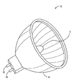
図1を参照すると、MR−16アウトライン・タイプの従来のハロゲン電球パッケージ10が示されている。ハロゲン電球パッケージには、ハロゲン電球によって生じる光を略均一な方向に向ける働きをする、リフレクタ14の中心に配置されたハロゲン電球12が含まれている。パッケージには、更に、電力を受信するため、1対の出力端子16及び18が含まれる。パッケージの前方開放面は、ダスト・カバー(不図示)によって保護することが可能である。図1のパッケージの欠点は、光源としてハロゲン電球を利用している点である。前述のように、ガラス・エンクロージャ及び白熱フィラメントの脆さのために、ハロゲン電球の動作寿命が制限される。
【0004】
上述の欠点に直面して、電球パッケージに可能性のある光源として発光ダイオードを利用することが検討されるようになった。発光ダイオード(LED)は、光スペクトルの特定領域にピーク波長を備える光を発生することが可能な周知の半導体素子である。従来、最も効率のよいLEDは、光スペクトルの赤領域にピーク波長を有する光、即ち、赤色光を放出する。しかし、最近になって、光スペクトルの青領域にピーク波長を有する光、即ち、青色光を効率よく放出することが可能な、窒化ガリウム(GaN)をベースにしたタイプのLEDが開発された。この新タイプのLEDによって、従来のLEDに比べて大幅に明るい出力光を得ることが可能になる。
【0005】
更に、青色光は、ピーク波長が赤色光より短いので、GaNベースのLEDによって発生する青色光をより容易に変換して、ピーク波長がより長い光を生じさせることが可能である。当該技術において周知のように、第1のピーク波長を備えた光(「一次光」)は、蛍光として知られるプロセスを利用して、ピーク波長がより長い光(「二次光」)に変換することが可能である。蛍光プロセスには、蛍光体材料の原子を励起するホトルミネッセント蛍光体材料によって一次光を吸収することと、二次光を放出することが必要とされる。蛍光プロセスを利用するLEDは、本明細書において、「蛍光体LED」と定義される。二次光のピーク波長は、蛍光体材料によって決まる。非変換一次光と二次光の合成光によって、蛍光体LEDの出力光が得られる。従って、出力光の特定のカラーは、一次光と二次光のスペクトル分布によって決まる。従って、電球パッケージは、GaNベースLEDに適した蛍光体材料を選択することによって、白色光を発生するように構成することが可能である。
【0006】
Vriens他に対する米国特許第5,813,753号には、エポキシ層に分散された蛍光体粒子を利用して、LEDによって放出される光のカラーを所望のカラーに変換する、光源としてLEDを備えた発光装置の記載がある。蛍光体粒子は、出力光の所望のカラーによって決まる、単一タイプの蛍光体材料、又は、異なる蛍光体材料の混合物として解説されている。Vriens他の特許に記載の蛍光体粒子を含むエポキシ層の利用に関する問題は、反復可能な均一なやり方で、蛍光体粒子を分配することの困難さである。こうした困難さのため、仕上がった一群の装置の性能にはばらつきがある、即ち、出力光のカラーが、仕上がった装置によって異なる可能性がある。
【0007】
【発明が解決しようとする課題】
以上の問題に鑑みて、本発明の目的は、規定のカラーの出力光を発生することが可能な光源として、蛍光体LEDを備える比較的単純で製造が容易である高性能の電球パッケージを提供することにあり、また、こうした電球パッケージの製造方法を提供することにある。
【0008】
【課題を解決するための手段】
LEDパッケージ及びLEDパッケージの製造方法には、アセンブリ前に、出力光のカラーに関してLEDパッケージの適正な性能を保証するため、光学特性を個別に検査することが可能な、蛍光物質を含む、あらかじめ製造された蛍光部材が利用されている。LEDパッケージには、パッケージの光源として機能する1つ以上のLEDダイが含まれている。あらかじめ製造された蛍光部材に含まれている蛍光物質、及び、LEDパッケージのLEDダイは、LEDパッケージによって生じる出力光が、自然白色光を再現するように淘汰的に選択されている。
【0009】
本発明の第1の実施形態の場合、LEDパッケージには、リード・フレームに取り付けられた個別リフレクタ・カップに個別に装着された、4つの3ボルト窒化ガリウム・ベースLEDダイが含まれている。この実施形態の場合、LEDパッケージは、工業規格MR−16ハロゲン・アウトライン・パッケージと互換性があるように構成されている。しかし、LEDパッケージは、MRC−11、MRC−16、PAR−36、PAR−38、PAR−56、及び、PAR−64といった他の工業規格パッケージに似るように構成することも可能である。実際のところ、LEDパッケージは、完全に異なる電球アウトライン・パッケージをなすように構成することが可能である。
【0010】
リード・フレームには、LEDダイに電力を供給する出力端子も取り付けられている。LEDダイは、特定の構成をなすように端子に電気的に接続されている。典型的な構成の1つでは、LEDダイは、直列に接続されているので、パッケージの全順方向電圧は、12ボルトになる。典型的な他の構成の場合、LEDダイは、6ボルト装置を形成するため、直列及び並列に接続される。LEDダイの正確な電気的構成、並びに、LEDダイの電圧は、本発明にとって重要ではない。更に、LEDパッケージに含まれるLEDダイの数も、本発明にとって重要ではない。
【0011】
LEDダイの上には、カプセル材料が堆積させられている。カプセル材料は、エポキシ又は他の適合する透明材料とすることが可能である。シリコン・ゲルは、高温にさらされるのに耐えることができ、劣化しないので、カプセル材料は、光学グレードのシリコン・ゲルが望ましい。更に、現在では、屈折率が1.5のシリコン・ゲルを利用可能であり、これによって、LEDダイによって発生する光が効率よく抽出されることになる。
【0012】
LEDパッケージの蛍光部材が、カプセル材料の上に固定される。この実施形態の場合、蛍光部材は、予め製造された光学的に透明な略平面のディスクである。しかし、蛍光部材は、LEDパッケージの仕様に従って、正方形又は矩形のような別の形状をなすように構成することも可能である。前述のようにして予め製造された蛍光部材に含まれる蛍光材料は、白色光を生じるように選択することが可能である。一例として、蛍光材料には、ガドリニウムをドープし、セリウムで活性化された、イットリウム・アルミニウム・ガーネット蛍光体粒子を含むことが可能である。
【0013】
LEDパッケージには、更に、蛍光部材に取り付けられたレンズと、レンズの上方に配置されたリフレクタが含まれている。レンズとリフレクタによって、LEDパッケージによって発生する光エネルギーの大部分が、確実に、略共通方向に沿って出力されることになる。
【0014】
本発明の第2の実施形態において、LEDパッケージのレンズは、凹レンズであり、蛍光部材は、凹レンズの内表面に形成される。蛍光部材自体、凹レンズの内表面の輪郭に形状適合する。この実施形態の場合、蛍光部材の光学特性は、レンズ及び取り付けられた蛍光部材を単一部品として検査して、検査することが可能である。
【0015】
本発明によるLEDパッケージの製造方法には、いくつかの透明な蛍光部材の形成が含まれている。第1の実施形態の場合、蛍光部材は、ディスクのように、略平面のプレートとすることが可能である。これらのプレートは、シリコン・ゴムのシートを所望の形状に切ることによって形成することが可能である。第2の実施形態の場合、蛍光部材は、凹面レンズの内表面に形状適合する非平面ディスクとすることが可能である。これらの非平面ディスクは、シリコン、ポリカーボネート、又は、アクリルのような光学的に透明な材料を、凹レンズの内表面上に成形できるようにすることによって、形成することが可能である。次に、光学特性について、蛍光部材の検査が行われる。一例として、蛍光部材は、標準的な単色光源を利用して、蛍光体を活性化し、次に、蛍光部材からの出力の特性を測定することによって検査可能である。次に、検査を受ける蛍光部材は、1組の光学特性に関して分類することが可能である。
【0016】
蛍光部材の検査が済むと、リード・フレームに1つ以上のGaNベースのLEDダイが取り付けられる。次に、透明なカプセル材料が、取り付けられたLEDダイの上に堆積させられる。カプセル材料は、熱安定性が高く、効率のよい光抽出にとって望ましい屈折率を備えた、光学グレードのシリコン・ゲルが望ましい。次に、事前定義された1組の光学特性を備えた蛍光部材が、カプセル材料上に配置される。次に、レンズが蛍光部材に取り付けられる。この工程は、第2の実施形態には適用することができない。次に、レンズの上方にリフレクタが取り付けられる。リフレクタの取り付けが済むと、リフレクタの縁にダスト・カバーを取り付けることによって、LEDパッケージが完成する。
【0017】
本発明の利点は、アセンブリの前に、蛍光部材の検査を行うことによって、仕上がった装置が特定の光学特性を備えることを保証することが可能になるので、望ましくない装置、即ち、所望の仕様を満たさない装置の製造に関連したコストが低下する。
【0018】
【発明の実施の形態】
図2を参照すると、第1の実施形態による典型的なLEDパッケージ20が示されている。図2は、LEDパッケージの略断面図である。LEDパッケージは、構造的に、従来のMR−16ハロゲン・パッケージに似るように構成されているので、LEDパッケージはMR−16パッケージとの互換性がある。しかし、LEDパッケージは、従来のMR−16パッケージの場合のように、ハロゲン電球ではなく、パッケージの光源として4つのLEDダイを利用している(図2で見えるのは、ダイ22及び24だけである)。LEDパッケージは、平均動作寿命が500乃至4000時間のハロゲン・パッケージに比べ、寿命が10,000時間以上である。更に、フィラメントの破損によって故障するハロゲン・パッケージとは異なり、LEDパッケージは、光出力の漸減によって劣化する。一般に、1,000時間の動作寿命の終了時において、LEDパッケージは、まだ、もとの光出力の50%を発生する。
【0019】
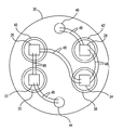
LEDパッケージ20には、円筒形ケーシング32の底部に取り付けられたリード・フレーム30が含まれている。一例として、リード・フレームは、鋼又は銅から構成することが可能である。このケーシングには、LEDパッケージによって生じた光の方向付けを行う正反射体も取り付けられている。次に図2及び3を参照すると、パッケージの4つのLED22、24、26、及び、28は、それぞれ、リフレクタ・カップ36、38、40、及び、42を介してリード・フレームに固定されている。LEDダイは、加えられた電気信号によって作動すると、青色光を放出する窒化ガリウム・ベースのLED(サファイア上のインジウムをドープした窒化ガリウム)であることが望ましい。リード・フレーム上におけるこのLEDダイ及びリフレクタ・カップの構成は、リード・フレームの平面図である図3に最も明瞭に示されている。LEDダイは、図2に最も明瞭に示されているように、リフレクタ・カップの空洞内に取り付けられている。リフレクタ・カップは、LEDダイに整合する熱膨張率(CTE)を備えた材料から製造するのが望ましい。一例として、リフレクタ・カップは、銀メッキしたモリブデンから製造することが可能である。リフレクタ・カップは、リード・フレームにスエージングされているので、LEDダイはリード・フレームに固定される。他の実施形態の場合、モリブデン・ディスク(図示せず)は、例えば、ハンダによって各LEDダイの下に取り付けられている。次に、LEDダイが取り付けられたモリブデン・ディスクは、リード・フレームに取り付けられる。この方法でも、所望のCTE整合が得られる。LEDダイは、リード・フレームにも取り付けられた、陽極端子44及び陰極端子46に電気的に接続されている。
【0020】
LEDパッケージ20に含めるように選択されたLEDダイ22、24、26、及び、28は、その最大定格駆動電流において、それぞれ、3ボルト未満の低順方向電圧による起動を可能にするタイプとすることが可能であり、従って、4つのLEDダイを直列に配線すると、公称12ボルトの全順方向電圧が生じることになる。図3には、この直列接続が例示されている。これによって、このパッケージは12ボルトの白熱パッケージに適合することになる。しかし、異なる直列電圧が必要とされる場合、LEDダイの他の構成を実施することも可能である。例えば、3つの4ボルトLEDダイを選択し、直列に配線して、12ボルトの同じ全順方向電圧を得ることも可能である。パッケージに含まれるLEDダイの正確なタイプ及び数と、LEDダイの接続構成は、製造すべき所望の装置に従って、変動する可能性がある。例えば、図4に示すように、4つの3ボルトLEDダイを直列/並列に配線すると、6ボルトの装置が得られる。LEDダイは、図2、図3、及び図4に示すように、ワイヤボンドによって電気的に接続することが可能である。図3に示すように、端子とLEDダイの間に駆動電流を伝送するため、2つ以上のワイヤを用いることが可能である。図2、図3、及び図4に示す電気接続は、ワイヤボンドによって施されるが、フリップ・チップ・ハンダ・バンピングのような、半導体産業において一般的な他の電気接続技法を代わりに利用することも可能である。
【0021】
LEDダイ22、24、26、及び、28は、測光パワーが有効範囲になるようなサイズであることが望ましい。これには、LEDダイのサイズが2.89平方ミリメートルになることを必要とする可能性があり、この結果、ダイにおける電流密度は70アンペア/平方センチメートルになる。例えば、これらのLEDダイの測光パワーは、5ルーメン(入力電力の1ワット当たり)であり、4つのダイのアセンブリに対する入力電力は、24ワット(2アンペアで12ボルト)である場合、全光出力パワーが5×24=120ルーメンの青色光になる。これを白色光に修正すると、白色光の典型的な出力は、1.9倍に上昇し、その結果、120×1.9=228ルーメンの最終白色光が得られることになる。
【0022】
図2を参照し直すと、LEDパッケージ20には、更に、LEDダイ上におけるカプセル材料の領域50が含まれている。LEDダイ22、24、26、及び、28から最大量の光を抽出するには、同様の屈折率を備えた光学グレードの材料が、LEDダイに接触していなければならない。サファイアLED基板は、一般に、2.5の屈折率を備えている。こうしたLEDは、一般に、屈折率が1.5の材料でカプセル封止(又はカプセル封じ)されている。スネルの法則を適用すると明らかなように、カプセル材料との界面の垂線に対する角度θが約0.644ラジアン(36.9度)の活性領域から放出される光だけが、LEDから脱出する。こうした場合、内部で発生した光の一部である1cosθ、即ち20%が抜け出ることになる。等しい量の光が、LEDダイの水平方向のエッジから放出される。LEDダイ22、24、26、又は28からのエッジ光は、LEDダイが取り付けられているリフレクタ・カップ36、38、40、又は42の反射空洞によって反射されて、順方向に送られる。
【0023】
屈折率の問題以外に、領域50のカプセル材料は、やはり、その動作中、LEDダイ22、24、26、及び、28によって生じる高温に耐えることができなければならない。LEDダイの表面温度は、容易に摂氏200度に達することが可能である。こうした状況下では、エポキシは、利用中、急速に熱劣化を被ることになり、漸次黄ばむようになって、LEDダイからの放射光の多くを吸収するので、装置が役に立たなくなる。以上の理由から、この領域に用いられるカプセル材料は、光学グレードのシリコン・ゲル材料から造られるのが望ましいが、エポキシのような、他のより望ましくない透明材料を利用することも可能である。シリコンは、優れた熱安定性を備えている。更に、光の抽出を最大にするため、屈折率が1.5のシリコン・ゲル材料を利用することも可能である。しかし、カプセル封止用のシリコン材料は、装置20の動作中、ボンド・ワイヤ48又はダイに応力を加えて、破壊することがないように、極めて柔らかくなければならない。これは、シリコンと装置本体(又はモリブデン・リフレクタ36、38、40、又は42)との膨張差によって生じる。一般に、これらのシリコン材料のCTEは、80PPM/単位長/゜Cである。金属本体(例えば、銅)のCTEは、約10乃至12PPM/単位長/゜Cであるため、装置のオン時とオフ時の膨張差は、8倍になり、この差によって、ボンド・ワイヤ又はダイに損傷を及ぼすのに十分なカプセル材料の移動を生じる可能性がある。
【0024】
カプセル材料の領域50に隣接して、蛍光材料を含む蛍光板52が配置されている。蛍光板52は、LEDパッケージのアセンブリ前に、光学特性を検査することが可能な事前製造部品である。蛍光板の検査は、蛍光板に含まれている蛍光体の均質性及び適正な蛍光体濃度に関連する。一例として、蛍光板は、軟質で、光学的に透明なシリコン・ゴムから造ることが可能である。しかし、蛍光板は、蛍光体を分散させた、ポリカーボネート又はアクリルのような他の光学的に透明な材料から造ることも可能である。蛍光板に含まれる蛍光体は、LEDパッケージ20によって発生する出力光の所望の波長特性によって決まる。一例として、蛍光板には、LEDダイ22、24、26、及び、28によって放出される青色放射光(波長が約460乃至480nm)の一部をより波長の長い放射光に変換するため、ガドリニウム(Gd)をドープし、セリウム(Ce)で活性化されたイットリウム・アルミニウム・ガーネット(YAG)蛍光体粒子(「Ce:YAG蛍光体粒子」)を含むことが可能である。Ce:YAG蛍光体粒子によって、蛍光板は、放出される青色光を吸収し、光エネルギーを約520nmの平均波長にアップシフトすることが可能になる。この結果生じる放出光は、480から620nmにわたる広帯域光である。この放出光と残りの青色光、即ち、非変換放出青色光との結合によって、自然白色光を再現する演色の最終放出光が生じることになる。
【0025】
上述の例の場合、蛍光板52は、サマリウム、プラセオジムといった他のいくつかの希土類金属を含めることによって修正を加え、LEDパッケージ20の演色を改良することが可能である。更に、他の蛍光体を加えることによって、他の波長の放出を生じさせ、LEDパッケージによって生じる出力光のスペクトル分布に修正を施すことも可能である。蛍光板に含まれている蛍光材料の正確なタイプは、本発明にとって重要ではない。
【0026】
例示の実施形態の場合、蛍光板52は、図3及び図4に示すように、リードフレーム30の形状に似た略平面のディスクである。しかし、LED22、24、26、及び、28が異なる形状に配置されて、リードフレームが非円形になる他の実施形態の場合、蛍光板は、リードフレーム、及び、取り付けられたLEDダイの形状に一致するように成形することが可能である。例えば、LEDパッケージのLEDダイが、矩形のリードフレーム上に矩形の形状に配置されている場合、蛍光板は、略平面の矩形プレートにすることが可能である。
【0027】
LEDパッケージ20には、更に、装置から放出される光を平行化して、リフレクタ34に均一に分配するため、蛍光板52に取り付けられたレンズ54が含まれている。レンズからの放射パターンは、レンズの上方に配置されたリフレクタに充満するように設計されている。一例として、レンズは、シリコンから造ることが可能である。あるいはまた、レンズは、ポリカーボネート又はアクリル材料から造ることが可能である。仕上がった装置を保護する働きをするダスト・カバー56がレンズの上方に配置され、リフレクタの縁に取り付けられる。
【0028】
次に図5を参照すると、第2の実施形態による典型的なLEDパッケージ60が示されている。図5のLEDパッケージには、図2におけるLEDパッケージの部品の大部分が含まれている。唯一の重要な相違は、LEDパッケージ20に含まれていたレンズ54及び蛍光板52が、凹面レンズ62及び成形された非平面蛍光ディスク64に置き換えられている点である。非平面蛍光ディスクは、凹面レンズの内表面に形成される。従って、レンズ及び成形非平面ディスクは、予め製造されるLEDパッケージの単一部品とされ得る。即ち、レンズ及び非平面ディスクは、パッケージの他の部品とは別個に、ユニットとして光学特性を検査することが可能な一体化部材になる。従って、この実施形態の場合、非平面蛍光ディスクの光学特性は、凹レンズの内表面に非平面蛍光ディスクが形成された後で、検査される。
【0029】
図2及び図5のLEDパッケージ20及び60は、MR−16タイプのアウトライン・パッケージとして例示し、解説してきたが、これらのLEDパッケージは、MRC−11、MRC−16、PAR−36、PAR−38、PAR−56、及び、PAR−64といった他のタイプの工業規格アウトライン・パッケージをなすように構成することも可能である。実際、LEDパッケージは、任意の構成をなすように配置された任意の数のLEDによって、完全に異なるアウトラインをなすように構成することが可能である。
【0030】
図6に関連して、図2及び図5のLEDパッケージ20及び60のようなLEDパッケージの製造方法について述べることにする。工程66において、光学的に透明ないくつかの蛍光部材が形成される。蛍光部材には、蛍光部材内に分散された蛍光体材料が含まれている。蛍光部材は、シリコン・ゴムから造られ、Ce:YAG蛍光体粒子を含んでいるのが望ましい。第1の実施形態の場合、蛍光部材は、整形されたプレートである。蛍光体材料を含む光学的に透明な材料のシートを製造すべきLEDパッケージの軸方向形状に一致する形状に切ることによって形成される。例えば、仕上がったプレートがディスク形状になるように形成することが可能である。第2の実施形態の場合、蛍光部材は、凹レンズの内表面に形状適合する非平面ディスクとして整形される。この実施形態の場合、蛍光部材は、蛍光材料が分散された、ポリカーボネート又はアクリルのような光学的に透明な材料を、凹レンズの輪郭を利用して、非平面ディスク形状をなすように成形することによって形成される。工程68において、蛍光部材は光学特性について検査を受ける。一例として、蛍光部材は、標準的な単色光源を利用して、蛍光体を活性化し、次に、蛍光部材からの出力を測定することによって、検査することが可能である。次に、検査された蛍光部材は、1組の光学特性に関して、「ビンに入れる」即ち分類することが可能である。同様の特性を示す蛍光部材を利用して、極めてよく似た光学特性の仕上がった装置が得られるようにすることが可能である。従って、色温度及び出力スペクトルに関して特定の顧客要求を満たす装置を生産することが可能である。光学特性は、装置の生産前に分かっているので、光学特性が所望の仕様を満たさない望ましくない装置は、回避されるので、生産コストが低下する。
【0031】
工程70において、1つ以上のGaNベースのLEDダイがリードフレームに取り付けられる。工程72において、LEDダイの上に、透明カプセル材料が堆積させられる。シリコン・ゲル材料は、熱特性が優れており、また、所望の屈折率を備えているので、カプセル材料として用いるのが好適である。次に、工程74において、特定の光学特性を有する検査を受けた蛍光部材が、カプセル材料の上に取り付けられる。透明なシリコン接着剤を利用して、蛍光部材をカプセル材料に取り付けることが可能である。あるいはまた、蛍光部材をカプセル材料にしっかりと押しつけることも可能である。次に、工程76において、蛍光部材にレンズが取り付けられる。カプセル材料に対する蛍光部材の取り付けと同様、レンズは、シリコン接着剤を利用するか、又は、レンズを蛍光部材にしっかりと押しつけることによって、蛍光部材に取り付けることが可能である。レンズ及び蛍光部材が単一の事前製造部品である第2の実施形態の場合、この工程は適用できない。工程78において、レンズの上に、リフレクタが取り付けられる。リフレクタの取り付けが済むと、工程80において、リフレクタの縁にダスト・カバーを取り付けることが可能になる。
【0032】
以上のように本発明の好適実施形態となる発光装置及びその製造方法について示したが、これはあくまでも例示的なものであり、当業者によって更に様々な変形変更が可能である。
【0033】
上述の実施形態に即して本発明を説明すると、本発明は、発光装置(20、60)を製造する方法にして、蛍光材料を含む光学部材(52、64)を形成する工程(66)と、前記発光装置の他の部品と共に前記光学部材を組み立てる前に、光学特性について、形成された前記光学部材を検査する工程(68)と、発光ダイオード(22、24、26、及び28)を含むアセンブリに対して前記光学部材を固定する工程が含まれており、前記光学部材を、前記発光ダイオードから放出される光の一部を変換することによって二次発光を生じさせ、前記発光ダイオードから放出される前記光の非変換部分と前記二次発光から構成される合成出力光が得られるように前記発光ダイオードに対して配置させることを特徴とする、発光装置(20、60)を製造する方法を提供する。
【0034】
好ましくは、前記光学部材(52、64)を形成する前記工程(66)は、前記蛍光材料を含む略平板状の透明板(52)を形成する工程である。
【0035】
好ましくは、平面の透明板(52)を形成する前記工程に、前記平面の透明板をディスク状プレートに整形する工程が含まれる。
【0036】
好ましくは、前記光学部材(52、64)を形成する工程(66)に、前記光学部材を前記発光素子のレンズ(62)の表面に対して形状適合させ、前記光学部材が前記レンズの一体化部品になるようにする工程が含まれる。
【0037】
好ましくは、前記アセンブリに前記光学部材(52、64)を固定する前記工程(74)の前に、更に前記アセンブリの前記発光ダイオード(22、24、26、及び28)にカプセル材料である光学グレードのシリコン・ゲルを付着させる工程が含まれる。
【0038】
更に本発明は、発光装置(20、60)であって、加えられる電気信号に応答して、第1のスペクトル分布を有する一次光を放出するための発光体(22、24、26、及び28)と、前記発光体に対して光学的に結合され、光学的に透明であり、蛍光体材料を含んでいて、前記一次光の一部が、前記蛍光体材料によって吸収されると、第2のスペクトル分布を有する二次光が放出されるようになっており、前記一次光と前記二次光が、前記装置によって発生する出力光のスペクトル分布を形成することになる、蛍光部材(52、64)と、前記蛍光部材を前記発光体に取り付けるための接続部材(50)が含まれていることを特徴とする発光装置(20、60)を提供する。
【0039】
好ましくは、前記蛍光部材(52、64)が、略平面のプレート(52)であって、該プレート(52)の面が、前記発光体から放出される前記一次光の方向に対して略垂直をなすように、前記発光体(22、24、26、及び28)に対して配置されている。
【0040】
好ましくは、前記略平面のプレート(52)が、ディスク状の構造に整形される。
【0041】
好ましくは、更に、前記蛍光部材(52、64)に一体化するように取り付けられたレンズ(62)が含まれていることと、前記蛍光部材が前記レンズの表面に対して形状適合することにより、前記蛍光部材と前記レンズが一体化ユニットになる。
【0042】
好ましくは、前記接続部材(50)に、前記発光体(22、24、26、及び28)をカプセル封止する光学グレードのシリコン・ゲルが含まれることと、前記光学グレードのシリコン・ゲルが、前記透明部材(52、64)と前記発光体の間に配置される。
【図面の簡単な説明】
【図1】MR−16アウトライン・タイプの従来のハロゲン電球に関する透視図である。
【図2】本発明の第1の実施形態によるLEDパッケージの断面図である。
【図3】取り付けられたLEDダイが動作電圧12ボルト構成をなすように電気的に接続されている、図2のLEDパッケージのリードフレームに関する平面図である。
【図4】取り付けられたLEDダイが動作電圧6ボルト構成をなすように電気的に接続されている、図2のLEDパッケージのリードフレームに関する平面図である。
【図5】本発明の第2の実施形態によるLEDパッケージの断面図である。
【図6】本発明によるLEDパッケージの製造方法に関する流れ図である。
【符号の説明】
20 発光装置
22 発光ダイオード
24 発光ダイオード
26 発光ダイオード
28 発光ダイオード
50 接続部材
52 光学部材
62 レンズ
64 光学部材[0001]
BACKGROUND OF THE INVENTION
The present invention relates generally to a light bulb package, and more particularly to a light bulb package type light emitting device including a light emitting diode using a fluorescent material as a light source, and a method of manufacturing the same.
[0002]
[Prior art]
A typical light bulb package utilizes a light source that includes an incandescent filament in a glass enclosure. However, these glass enclosures are fragile and can themselves easily break even if they are subjected to a modest impact. Furthermore, the incandescent filament itself is fragile and tends to deteriorate gradually during use, and the effective light output produced by the filament decreases with time. As the fragility of the filament increases with age, it eventually breaks and breaks. Typical incandescent bulbs have an average lifetime of 500 to 4000 hours, which means that half of a group of bulbs will fail within that time due to filament breakage.
[0003]
Referring to FIG. 1, a conventional
[0004]
In the face of the above drawbacks, the use of light emitting diodes as a potential light source for bulb packages has been considered. A light emitting diode (LED) is a well-known semiconductor element capable of generating light having a peak wavelength in a specific region of the light spectrum. Conventionally, the most efficient LEDs emit light having a peak wavelength in the red region of the light spectrum, i.e. red light. Recently, however, LEDs of the type based on gallium nitride (GaN) have been developed that can efficiently emit light having a peak wavelength in the blue region of the light spectrum, that is, blue light. This new type of LED makes it possible to obtain output light that is significantly brighter than conventional LEDs.
[0005]
Furthermore, since blue light has a shorter peak wavelength than red light, blue light generated by GaN-based LEDs can be more easily converted to produce light with a longer peak wavelength. As is well known in the art, light with a first peak wavelength (“primary light”) is converted to light with a longer peak wavelength (“secondary light”) using a process known as fluorescence. Is possible. The fluorescence process requires absorbing primary light and emitting secondary light by a photoluminescent phosphor material that excites the atoms of the phosphor material. An LED that utilizes a fluorescent process is defined herein as a “phosphor LED”. The peak wavelength of the secondary light depends on the phosphor material. The output light of the phosphor LED is obtained by the combined light of the non-converted primary light and the secondary light. Therefore, the specific color of the output light is determined by the spectral distribution of the primary light and the secondary light. Thus, the bulb package can be configured to generate white light by selecting a phosphor material suitable for a GaN-based LED.
[0006]
U.S. Pat. No. 5,813,753 to Vries et al. Includes an LED as a light source that utilizes phosphor particles dispersed in an epoxy layer to convert the color of light emitted by the LED to a desired color. There is a description of a light emitting device. The phosphor particles are described as a single type of phosphor material or a mixture of different phosphor materials, depending on the desired color of the output light. A problem with the use of epoxy layers containing phosphor particles as described in the Vries et al. Patent is the difficulty of dispensing the phosphor particles in a repeatable and uniform manner. Because of these difficulties, the performance of a group of finished devices varies, i.e., the color of the output light can vary from one finished device to another.
[0007]
[Problems to be solved by the invention]
In view of the above problems, an object of the present invention is to provide a relatively simple and easy-to-manufacture high-performance light bulb package that includes a phosphor LED as a light source capable of generating output light of a prescribed color. It is also to provide a method for manufacturing such a light bulb package.
[0008]
[Means for Solving the Problems]
The LED package and the LED package manufacturing method include a pre-manufactured product that includes a phosphor that can be individually inspected for optical properties to ensure proper performance of the LED package with respect to the color of the output light prior to assembly. The fluorescent member made is used. The LED package includes one or more LED dies that function as a light source for the package. The fluorescent material contained in the pre-manufactured fluorescent member and the LED die of the LED package are selected so that the output light generated by the LED package reproduces natural white light.
[0009]
For the first embodiment of the present invention, the LED package includes four 3 volt gallium nitride based LED dies that are individually attached to individual reflector cups attached to the lead frame. In this embodiment, the LED package is configured to be compatible with the industry standard MR-16 halogen outline package. However, the LED package can also be configured to resemble other industry standard packages such as MRC-11, MRC-16, PAR-36, PAR-38, PAR-56, and PAR-64. In fact, the LED package can be configured to form a completely different bulb outline package.
[0010]
An output terminal for supplying power to the LED die is also attached to the lead frame. The LED die is electrically connected to the terminal so as to have a specific configuration. In one typical configuration, the LED dies are connected in series, so the total forward voltage of the package is 12 volts. In another typical configuration, the LED dies are connected in series and in parallel to form a 6 volt device. The exact electrical configuration of the LED die, as well as the LED die voltage, is not critical to the present invention. Further, the number of LED dies included in the LED package is not critical to the present invention.
[0011]
A capsule material is deposited on the LED die. The encapsulant material can be epoxy or other suitable transparent material. Since silicon gels can withstand exposure to high temperatures and do not degrade, the encapsulant material is preferably an optical grade silicon gel. In addition, silicon gel with a refractive index of 1.5 is currently available, which effectively extracts the light generated by the LED die.
[0012]
The fluorescent member of the LED package is fixed on the encapsulant material. In this embodiment, the fluorescent member is an optically transparent substantially flat disk manufactured in advance. However, the fluorescent member may be configured to have another shape such as a square or a rectangle according to the specification of the LED package. The fluorescent material contained in the fluorescent member manufactured in advance as described above can be selected so as to generate white light. As an example, the fluorescent material may include yttrium aluminum garnet phosphor particles doped with gadolinium and activated with cerium.
[0013]
The LED package further includes a lens attached to the fluorescent member and a reflector disposed above the lens. The lens and reflector ensure that most of the light energy generated by the LED package is output along a substantially common direction.
[0014]
In the second embodiment of the present invention, the lens of the LED package is a concave lens, and the fluorescent member is formed on the inner surface of the concave lens. The fluorescent member itself conforms to the contour of the inner surface of the concave lens. In the case of this embodiment, the optical characteristics of the fluorescent member can be inspected by inspecting the lens and the attached fluorescent member as a single part.
[0015]
The method for manufacturing an LED package according to the present invention includes forming several transparent fluorescent members. In the case of the first embodiment, the fluorescent member can be a substantially flat plate like a disk. These plates can be formed by cutting a sheet of silicon rubber into the desired shape. In the case of the second embodiment, the fluorescent member can be a non-planar disk that conforms to the inner surface of the concave lens. These non-planar discs can be formed by allowing an optically transparent material such as silicon, polycarbonate, or acrylic to be molded onto the inner surface of the concave lens. Next, the fluorescent member is inspected for optical characteristics. As an example, the fluorescent member can be inspected by activating the phosphor using a standard monochromatic light source and then measuring the characteristics of the output from the fluorescent member. Next, the fluorescent member to be inspected can be classified with respect to a set of optical properties.
[0016]
Once the fluorescent member is inspected, one or more GaN-based LED dies are attached to the lead frame. A transparent encapsulant is then deposited on the attached LED die. The encapsulant material is preferably an optical grade silicone gel with high thermal stability and a refractive index that is desirable for efficient light extraction. Next, a fluorescent member with a predefined set of optical properties is placed on the capsule material. Next, a lens is attached to the fluorescent member. This process cannot be applied to the second embodiment. Next, a reflector is attached above the lens. When the reflector is attached, the LED package is completed by attaching a dust cover to the edge of the reflector.
[0017]
An advantage of the present invention is that it is possible to ensure that the finished device has specific optical properties by performing an inspection of the fluorescent member prior to assembly, so that the undesired device, i.e. the desired specification. The costs associated with manufacturing devices that do not meet are reduced.
[0018]
DETAILED DESCRIPTION OF THE INVENTION
Referring to FIG. 2, an
[0019]
The
[0020]
The LED dies 22, 24, 26, and 28 selected to be included in the
[0021]
The LED dies 22, 24, 26, and 28 are desirably sized so that the photometric power is within the effective range. This may require the LED die size to be 2.89 square millimeters, resulting in a current density in the die of 70 amps / square centimeter. For example, the metering power of these LED dies is 5 lumens (per watt of input power), and the input power for a four-die assembly is 24 watts (2 volts, 12 volts), the total light output The power becomes 5 × 24 = 120 lumen blue light. Correcting this to white light increases the typical output of white light by a factor of 1.9, resulting in a final white light of 120 × 1.9 = 228 lumens.
[0022]
Referring back to FIG. 2, the
[0023]
Besides the refractive index problem, the encapsulant in
[0024]
A
[0025]
In the above example, the
[0026]
In the illustrated embodiment, the
[0027]
The
[0028]
Referring now to FIG. 5, a
[0029]
2 and 5 have been illustrated and described as MR-16 type outline packages, these LED packages are MRC-11, MRC-16, PAR-36, PAR- Other types of industry standard outline packages such as 38, PAR-56, and PAR-64 can also be configured. In fact, an LED package can be configured to have a completely different outline with any number of LEDs arranged in any configuration.
[0030]
With reference to FIG. 6, a method for manufacturing LED packages such as LED packages 20 and 60 of FIGS. 2 and 5 will be described. In
[0031]
In
[0032]
As described above, the light emitting device and the manufacturing method thereof according to the preferred embodiment of the present invention have been described. However, this is merely an example, and various modifications and changes can be made by those skilled in the art.
[0033]
The present invention will be described with reference to the above-described embodiment. The present invention provides a method (66) of forming an optical member (52, 64) containing a fluorescent material by a method of manufacturing a light emitting device (20, 60). And (68) inspecting the formed optical member for optical properties before assembling the optical member with other components of the light emitting device, and light emitting diodes (22, 24, 26, and 28). Securing the optical member to an assembly that includes the optical member causing secondary light emission by converting a portion of the light emitted from the light emitting diode; from the light emitting diode; A light emitting device (20, 6), wherein the light emitting diode (20, 6) is arranged so as to obtain a combined output light composed of a non-converted portion of the emitted light and the secondary light emission. ) Provides a method for producing a.
[0034]
Preferably, the step (66) of forming the optical member (52, 64) is a step of forming a substantially flat transparent plate (52) containing the fluorescent material.
[0035]
Preferably, the step of forming the flat transparent plate (52) includes a step of shaping the flat transparent plate into a disk-shaped plate.
[0036]
Preferably, in the step (66) of forming the optical member (52, 64), the shape of the optical member is adapted to the surface of the lens (62) of the light emitting element, and the optical member is integrated with the lens. The process of becoming a part is included.
[0037]
Preferably, before the step (74) of fixing the optical member (52, 64) to the assembly, and further to the light emitting diode (22, 24, 26, and 28) of the assembly, an optical grade that is an encapsulating material. Depositing the silicon gel.
[0038]
The present invention further relates to a light emitting device (20, 60) for emitting primary light having a first spectral distribution in response to an applied electrical signal (22, 24, 26, and 28). ), And optically coupled to the light emitter, optically transparent, including a phosphor material, and when a portion of the primary light is absorbed by the phosphor material, the second Secondary light having the following spectral distribution is emitted, and the primary light and the secondary light form a spectral distribution of output light generated by the device, the fluorescent member (52, 64) and a connecting member (50) for attaching the fluorescent member to the light emitter, a light emitting device (20, 60) is provided.
[0039]
Preferably, the fluorescent member (52, 64) is a substantially flat plate (52), and the surface of the plate (52) is substantially perpendicular to the direction of the primary light emitted from the light emitter. The light emitters (22, 24, 26, and 28) are arranged so as to form
[0040]
Preferably, the substantially planar plate (52) is shaped into a disk-like structure.
[0041]
Preferably, it further includes a lens (62) attached so as to be integrated with the fluorescent member (52, 64), and that the fluorescent member conforms to the surface of the lens. The fluorescent member and the lens form an integrated unit.
[0042]
Preferably, the connecting member (50) includes an optical grade silicone gel that encapsulates the light emitters (22, 24, 26, and 28), and the optical grade silicone gel comprises: It arrange | positions between the said transparent member (52, 64) and the said light-emitting body.
[Brief description of the drawings]
FIG. 1 is a perspective view of a conventional halogen bulb of the MR-16 outline type.
FIG. 2 is a cross-sectional view of an LED package according to the first embodiment of the present invention.
3 is a top view of the lead frame of the LED package of FIG. 2 with the attached LED dies electrically connected to form a 12 volt operating voltage configuration.
4 is a plan view of the lead frame of the LED package of FIG. 2 with the attached LED dies electrically connected to form a 6 volt operating voltage configuration.
FIG. 5 is a cross-sectional view of an LED package according to a second embodiment of the present invention.
FIG. 6 is a flowchart for a method of manufacturing an LED package according to the present invention.
[Explanation of symbols]
20 Light emitting device
22 Light emitting diode
24 light emitting diode
26 Light Emitting Diode
28 Light Emitting Diode
50 Connecting members
52 Optical members
62 lenses
64 Optical members
Claims (3)
前記光学部材の各々を、前記出力の特性に基づいて複数に分類し、
光を放射する発光素子をアセンブリに設け、
前記出力の特性に基づいて分類された前記光学部材から所定の光学部材を選択し、
選択された前記光学部材を前記アセンブリに固定する、方法であって、
前記出力の特性と前記光の波長特性との組合せは、白色光を再現するように選択されている、
方法。Each of the plurality of optical members, including a fluorescent material, the fluorescent material activated using the standard monochromatic light source, by measuring the characteristics of the output from the fluorescent material, inspected,
Each of the optical member, are classified into a plurality based on the characteristics of the output,
A light emitting element for emitting light is provided in the assembly;
Selecting a predetermined optical member from the optical member that is classified based on the characteristics of the output,
Fixing the optical member that is selected in the assembly, a method,
Set combined with the wavelength characteristics of the optical characteristic of the output is selected to reproduce the white light,
Method.
Applications Claiming Priority (2)
| Application Number | Priority Date | Filing Date | Title |
|---|---|---|---|
| US09/390,006 US6504301B1 (en) | 1999-09-03 | 1999-09-03 | Non-incandescent lightbulb package using light emitting diodes |
| US390006 | 1999-09-03 |
Related Child Applications (1)
| Application Number | Title | Priority Date | Filing Date |
|---|---|---|---|
| JP2011096108A Division JP5580246B2 (en) | 1999-09-03 | 2011-04-22 | Method for manufacturing light emitting device using light emitting diode |
Publications (2)
| Publication Number | Publication Date |
|---|---|
| JP2001111117A JP2001111117A (en) | 2001-04-20 |
| JP5116912B2 true JP5116912B2 (en) | 2013-01-09 |
Family
ID=23540657
Family Applications (2)
| Application Number | Title | Priority Date | Filing Date |
|---|---|---|---|
| JP2000249758A Expired - Lifetime JP5116912B2 (en) | 1999-09-03 | 2000-08-21 | Light emitting device using light emitting diode and method for manufacturing the same |
| JP2011096108A Expired - Lifetime JP5580246B2 (en) | 1999-09-03 | 2011-04-22 | Method for manufacturing light emitting device using light emitting diode |
Family Applications After (1)
| Application Number | Title | Priority Date | Filing Date |
|---|---|---|---|
| JP2011096108A Expired - Lifetime JP5580246B2 (en) | 1999-09-03 | 2011-04-22 | Method for manufacturing light emitting device using light emitting diode |
Country Status (3)
| Country | Link |
|---|---|
| US (1) | US6504301B1 (en) |
| EP (1) | EP1081771B1 (en) |
| JP (2) | JP5116912B2 (en) |
Families Citing this family (370)
| Publication number | Priority date | Publication date | Assignee | Title |
|---|---|---|---|---|
| US6600175B1 (en) * | 1996-03-26 | 2003-07-29 | Advanced Technology Materials, Inc. | Solid state white light emitter and display using same |
| US7014336B1 (en) * | 1999-11-18 | 2006-03-21 | Color Kinetics Incorporated | Systems and methods for generating and modulating illumination conditions |
| US7064498B2 (en) * | 1997-08-26 | 2006-06-20 | Color Kinetics Incorporated | Light-emitting diode based products |
| US6806659B1 (en) | 1997-08-26 | 2004-10-19 | Color Kinetics, Incorporated | Multicolored LED lighting method and apparatus |
| US7352339B2 (en) * | 1997-08-26 | 2008-04-01 | Philips Solid-State Lighting Solutions | Diffuse illumination systems and methods |
| US20030133292A1 (en) * | 1999-11-18 | 2003-07-17 | Mueller George G. | Methods and apparatus for generating and modulating white light illumination conditions |
| US7482764B2 (en) * | 1997-08-26 | 2009-01-27 | Philips Solid-State Lighting Solutions, Inc. | Light sources for illumination of liquids |
| US7038398B1 (en) * | 1997-08-26 | 2006-05-02 | Color Kinetics, Incorporated | Kinetic illumination system and methods |
| US20020176259A1 (en) * | 1999-11-18 | 2002-11-28 | Ducharme Alfred D. | Systems and methods for converting illumination |
| DE10006286C1 (en) * | 2000-02-14 | 2001-10-18 | 3M Espe Ag | Light wave converter device and its use in the dental field |
| PT1422975E (en) * | 2000-04-24 | 2010-07-09 | Philips Solid State Lighting | Light-emitting diode based product |
| AUPR570501A0 (en) * | 2001-06-15 | 2001-07-12 | Q1 (Pacific) Limited | Led lamp |
| JP4066620B2 (en) * | 2000-07-21 | 2008-03-26 | 日亜化学工業株式会社 | LIGHT EMITTING ELEMENT, DISPLAY DEVICE HAVING LIGHT EMITTING ELEMENT AND METHOD FOR MANUFACTURING DISPLAY DEVICE |
| TW490863B (en) * | 2001-02-12 | 2002-06-11 | Arima Optoelectronics Corp | Manufacturing method of LED with uniform color temperature |
| JP4101468B2 (en) * | 2001-04-09 | 2008-06-18 | 豊田合成株式会社 | Method for manufacturing light emitting device |
| US6878972B2 (en) * | 2001-06-08 | 2005-04-12 | Agilent Technologies, Inc. | Light-emitting diode with plastic reflector cup |
| JP2003110146A (en) * | 2001-07-26 | 2003-04-11 | Matsushita Electric Works Ltd | Light-emitting device |
| ATE356532T1 (en) | 2001-09-13 | 2007-03-15 | Lucea Ag | LED LIGHT PANEL AND CIRCUIT BOARD |
| WO2003038334A1 (en) * | 2001-10-24 | 2003-05-08 | Koenecke Dirk | Luminous element |
| US6871983B2 (en) | 2001-10-25 | 2005-03-29 | Tir Systems Ltd. | Solid state continuous sealed clean room light fixture |
| US7497596B2 (en) * | 2001-12-29 | 2009-03-03 | Mane Lou | LED and LED lamp |
| US6711426B2 (en) * | 2002-04-09 | 2004-03-23 | Spectros Corporation | Spectroscopy illuminator with improved delivery efficiency for high optical density and reduced thermal load |
| US20080009689A1 (en) * | 2002-04-09 | 2008-01-10 | Benaron David A | Difference-weighted somatic spectroscopy |
| CA2427559A1 (en) * | 2002-05-15 | 2003-11-15 | Sumitomo Electric Industries, Ltd. | White color light emitting device |
| US10340424B2 (en) | 2002-08-30 | 2019-07-02 | GE Lighting Solutions, LLC | Light emitting diode component |
| US7800121B2 (en) * | 2002-08-30 | 2010-09-21 | Lumination Llc | Light emitting diode component |
| US7224000B2 (en) | 2002-08-30 | 2007-05-29 | Lumination, Llc | Light emitting diode component |
| ES2335878T3 (en) * | 2002-08-30 | 2010-04-06 | Lumination, Llc | COVERED LED WITH IMPROVED EFFECTIVENESS. |
| US7264378B2 (en) * | 2002-09-04 | 2007-09-04 | Cree, Inc. | Power surface mount light emitting die package |
| US7244965B2 (en) | 2002-09-04 | 2007-07-17 | Cree Inc, | Power surface mount light emitting die package |
| US7775685B2 (en) | 2003-05-27 | 2010-08-17 | Cree, Inc. | Power surface mount light emitting die package |
| JP4201167B2 (en) * | 2002-09-26 | 2008-12-24 | シチズン電子株式会社 | Manufacturing method of white light emitting device |
| JP4280050B2 (en) | 2002-10-07 | 2009-06-17 | シチズン電子株式会社 | White light emitting device |
| US6896381B2 (en) * | 2002-10-11 | 2005-05-24 | Light Prescriptions Innovators, Llc | Compact folded-optics illumination lens |
| US7554258B2 (en) * | 2002-10-22 | 2009-06-30 | Osram Opto Semiconductors Gmbh | Light source having an LED and a luminescence conversion body and method for producing the luminescence conversion body |
| US20040141321A1 (en) * | 2002-11-20 | 2004-07-22 | Color Kinetics, Incorporated | Lighting and other perceivable effects for toys and other consumer products |
| US7042655B2 (en) * | 2002-12-02 | 2006-05-09 | Light Prescriptions Innovators, Llc | Apparatus and method for use in fulfilling illumination prescription |
| MXPA05005658A (en) | 2002-12-02 | 2005-08-16 | 3M Innovative Properties Co | Illumination system using a plurality of light sources. |
| US7312560B2 (en) * | 2003-01-27 | 2007-12-25 | 3M Innovative Properties | Phosphor based light sources having a non-planar long pass reflector and method of making |
| US20040145312A1 (en) * | 2003-01-27 | 2004-07-29 | 3M Innovative Properties Company | Phosphor based light source having a flexible short pass reflector |
| US7245072B2 (en) * | 2003-01-27 | 2007-07-17 | 3M Innovative Properties Company | Phosphor based light sources having a polymeric long pass reflector |
| US7118438B2 (en) * | 2003-01-27 | 2006-10-10 | 3M Innovative Properties Company | Methods of making phosphor based light sources having an interference reflector |
| JP2006516828A (en) * | 2003-01-27 | 2006-07-06 | スリーエム イノベイティブ プロパティズ カンパニー | Phosphorescent light source element and manufacturing method |
| US7091653B2 (en) | 2003-01-27 | 2006-08-15 | 3M Innovative Properties Company | Phosphor based light sources having a non-planar long pass reflector |
| US20040145289A1 (en) * | 2003-01-27 | 2004-07-29 | 3M Innovative Properties Company | Phosphor based light sources having a non-planar short pass reflector and method of making |
| US7091661B2 (en) * | 2003-01-27 | 2006-08-15 | 3M Innovative Properties Company | Phosphor based light sources having a reflective polarizer |
| US20040159900A1 (en) * | 2003-01-27 | 2004-08-19 | 3M Innovative Properties Company | Phosphor based light sources having front illumination |
| US7377671B2 (en) * | 2003-02-04 | 2008-05-27 | Light Prescriptions Innovators, Llc | Etendue-squeezing illumination optics |
| EP2365095A1 (en) | 2003-02-26 | 2011-09-14 | Callida Genomics, Inc. | Random array DNA analysis by hybridization |
| DE10308866A1 (en) * | 2003-02-28 | 2004-09-09 | Osram Opto Semiconductors Gmbh | Lighting module and method for its production |
| EP1455398A3 (en) * | 2003-03-03 | 2011-05-25 | Toyoda Gosei Co., Ltd. | Light emitting device comprising a phosphor layer and method of making same |
| US20040189555A1 (en) * | 2003-03-26 | 2004-09-30 | Capen Larry Stephen | Use of track lighting switching power supplies to efficiently drive LED arrays |
| US20070020578A1 (en) * | 2005-07-19 | 2007-01-25 | Scott Robert R | Dental curing light having a short wavelength LED and a fluorescing lens for converting wavelength light to curing wavelengths and related method |
| US7005679B2 (en) | 2003-05-01 | 2006-02-28 | Cree, Inc. | Multiple component solid state white light |
| CN1802533B (en) * | 2003-05-05 | 2010-11-24 | 吉尔科有限公司 | LED-based light bulb |
| US7329029B2 (en) | 2003-05-13 | 2008-02-12 | Light Prescriptions Innovators, Llc | Optical device for LED-based lamp |
| US8075147B2 (en) * | 2003-05-13 | 2011-12-13 | Light Prescriptions Innovators, Llc | Optical device for LED-based lamp |
| US6921182B2 (en) * | 2003-05-13 | 2005-07-26 | Solaroasis | Efficient LED lamp for enhancing commercial and home plant growth |
| US7021797B2 (en) * | 2003-05-13 | 2006-04-04 | Light Prescriptions Innovators, Llc | Optical device for repositioning and redistributing an LED's light |
| JP4138586B2 (en) | 2003-06-13 | 2008-08-27 | スタンレー電気株式会社 | LED lamp for light source and vehicle headlamp using the same |
| AT412928B (en) | 2003-06-18 | 2005-08-25 | Guenther Dipl Ing Dr Leising | METHOD FOR PRODUCING A WHITE LED AND WHITE LED LIGHT SOURCE |
| US7145125B2 (en) * | 2003-06-23 | 2006-12-05 | Advanced Optical Technologies, Llc | Integrating chamber cone light using LED sources |
| US7521667B2 (en) * | 2003-06-23 | 2009-04-21 | Advanced Optical Technologies, Llc | Intelligent solid state lighting |
| US7462983B2 (en) * | 2003-06-27 | 2008-12-09 | Avago Technologies Ecbu Ip (Singapore) Pte. Ltd. | White light emitting device |
| WO2005012951A2 (en) * | 2003-07-28 | 2005-02-10 | Light Prescriptions Innovators, Llc | Three-dimensional simultaneous multiple-surface method and free-form illumination-optics designed therefrom |
| WO2005012952A2 (en) * | 2003-07-29 | 2005-02-10 | Light Prescriptions Innovators, Llc | Circumferentially emitting luminaires and lens elements formed by transverse-axis profile-sweeps |
| US7009213B2 (en) * | 2003-07-31 | 2006-03-07 | Lumileds Lighting U.S., Llc | Light emitting devices with improved light extraction efficiency |
| US7679096B1 (en) | 2003-08-21 | 2010-03-16 | Opto Technology, Inc. | Integrated LED heat sink |
| EP1668960A2 (en) * | 2003-09-08 | 2006-06-14 | Nanocrystal Lighting Corporation | Light efficient packaging configurations for led lamps using high refractive index encapsulants |
| US7029935B2 (en) * | 2003-09-09 | 2006-04-18 | Cree, Inc. | Transmissive optical elements including transparent plastic shell having a phosphor dispersed therein, and methods of fabricating same |
| US7300173B2 (en) | 2004-04-08 | 2007-11-27 | Technology Assessment Group, Inc. | Replacement illumination device for a miniature flashlight bulb |
| US7777430B2 (en) | 2003-09-12 | 2010-08-17 | Terralux, Inc. | Light emitting diode replacement lamp |
| JP4140042B2 (en) | 2003-09-17 | 2008-08-27 | スタンレー電気株式会社 | LED light source device using phosphor and vehicle headlamp using LED light source device |
| US7052152B2 (en) * | 2003-10-03 | 2006-05-30 | Philips Lumileds Lighting Company, Llc | LCD backlight using two-dimensional array LEDs |
| JP4402425B2 (en) | 2003-10-24 | 2010-01-20 | スタンレー電気株式会社 | Vehicle headlamp |
| DE10351349A1 (en) * | 2003-10-31 | 2005-06-16 | Osram Opto Semiconductors Gmbh | Production of a luminescent diode chip applies a radiation decoupling surface and a semiconductor body with an epitaxial-grown sequence of semiconductor layers with an active zone |
| DE10351397A1 (en) * | 2003-10-31 | 2005-06-16 | Osram Opto Semiconductors Gmbh | LED chip |
| US8632215B2 (en) | 2003-11-04 | 2014-01-21 | Terralux, Inc. | Light emitting diode replacement lamp |
| JP4385741B2 (en) * | 2003-11-25 | 2009-12-16 | パナソニック電工株式会社 | Light emitting device |
| EP1691425B1 (en) * | 2003-11-25 | 2010-08-11 | Panasonic Electric Works Co., Ltd. | Light emitting device using light emitting diode chip |
| US20050116635A1 (en) * | 2003-12-02 | 2005-06-02 | Walson James E. | Multiple LED source and method for assembling same |
| US7250611B2 (en) | 2003-12-02 | 2007-07-31 | 3M Innovative Properties Company | LED curing apparatus and method |
| WO2005078338A1 (en) | 2004-02-17 | 2005-08-25 | Kelly William M | A utility lamp |
| US7517728B2 (en) | 2004-03-31 | 2009-04-14 | Cree, Inc. | Semiconductor light emitting devices including a luminescent conversion element |
| US7837348B2 (en) | 2004-05-05 | 2010-11-23 | Rensselaer Polytechnic Institute | Lighting system using multiple colored light emitting sources and diffuser element |
| WO2005107420A2 (en) * | 2004-05-05 | 2005-11-17 | Rensselaer Polytechnic Institute | High efficiency light source using solid-state emitter and down-conversion material |
| US8227820B2 (en) | 2005-02-09 | 2012-07-24 | The Regents Of The University Of California | Semiconductor light-emitting device |
| US7781789B2 (en) | 2006-11-15 | 2010-08-24 | The Regents Of The University Of California | Transparent mirrorless light emitting diode |
| US7768023B2 (en) | 2005-10-14 | 2010-08-03 | The Regents Of The University Of California | Photonic structures for efficient light extraction and conversion in multi-color light emitting devices |
| US8860051B2 (en) | 2006-11-15 | 2014-10-14 | The Regents Of The University Of California | Textured phosphor conversion layer light emitting diode |
| US7070300B2 (en) | 2004-06-04 | 2006-07-04 | Philips Lumileds Lighting Company, Llc | Remote wavelength conversion in an illumination device |
| US7553683B2 (en) * | 2004-06-09 | 2009-06-30 | Philips Lumiled Lighting Co., Llc | Method of forming pre-fabricated wavelength converting elements for semiconductor light emitting devices |
| US7256057B2 (en) * | 2004-09-11 | 2007-08-14 | 3M Innovative Properties Company | Methods for producing phosphor based light sources |
| JP4823505B2 (en) * | 2004-10-20 | 2011-11-24 | シャープ株式会社 | Semiconductor device and electronic equipment |
| US20060097385A1 (en) * | 2004-10-25 | 2006-05-11 | Negley Gerald H | Solid metal block semiconductor light emitting device mounting substrates and packages including cavities and heat sinks, and methods of packaging same |
| JP2006128562A (en) | 2004-11-01 | 2006-05-18 | Nikon Corp | Light emitting device |
| DE112005002889B4 (en) | 2004-12-14 | 2015-07-23 | Seoul Viosys Co., Ltd. | Light emitting device with a plurality of light emitting cells and assembly assembly thereof |
| DE102004060475A1 (en) * | 2004-12-16 | 2006-07-06 | Hella Kgaa Hueck & Co. | Head light for vehicles has light-converting luminescent material is designed as light-converting luminescent coating which exhibits given contour and a defined irradiancy is generated on the light-converting luminescent material coating |
| US20060139580A1 (en) * | 2004-12-29 | 2006-06-29 | Conner Arlie R | Illumination system using multiple light sources with integrating tunnel and projection systems using same |
| US7564180B2 (en) | 2005-01-10 | 2009-07-21 | Cree, Inc. | Light emission device and method utilizing multiple emitters and multiple phosphors |
| US8125137B2 (en) | 2005-01-10 | 2012-02-28 | Cree, Inc. | Multi-chip light emitting device lamps for providing high-CRI warm white light and light fixtures including the same |
| JP4634810B2 (en) * | 2005-01-20 | 2011-02-16 | 信越化学工業株式会社 | Silicone sealed LED |
| EP1854154A2 (en) * | 2005-02-16 | 2007-11-14 | Koninklijke Philips Electronics N.V. | Light emitting device comprising inorganic light emitting diode(s) |
| JP5373243B2 (en) * | 2005-02-24 | 2013-12-18 | 株式会社朝日ラバー | Light-emitting diode lens component and light-emitting diode light source device |
| WO2006095949A1 (en) | 2005-03-11 | 2006-09-14 | Seoul Semiconductor Co., Ltd. | Led package having an array of light emitting cells coupled in series |
| US7316497B2 (en) * | 2005-03-29 | 2008-01-08 | 3M Innovative Properties Company | Fluorescent volume light source |
| KR101402190B1 (en) | 2005-05-25 | 2014-06-03 | 코닌클리케 필립스 엔.브이. | Electroluminescence device |
| WO2006131924A2 (en) | 2005-06-07 | 2006-12-14 | Oree, Advanced Illumination Solutions Inc. | Illumination apparatus |
| US8272758B2 (en) | 2005-06-07 | 2012-09-25 | Oree, Inc. | Illumination apparatus and methods of forming the same |
| US8215815B2 (en) * | 2005-06-07 | 2012-07-10 | Oree, Inc. | Illumination apparatus and methods of forming the same |
| WO2006138626A2 (en) | 2005-06-17 | 2006-12-28 | The Regents Of The University Of California | (AI,Ga,In)N AND ZnO DIRECT WAFER BONDED STRUCTURE FOR OPTOELECTRONIC APPLICATION AND ITS FABRICATION METHOD |
| CN101203965B (en) * | 2005-06-23 | 2010-04-21 | 皇家飞利浦电子股份有限公司 | A light-emitting device and method for its design |
| DE102005038698A1 (en) * | 2005-07-08 | 2007-01-18 | Tridonic Optoelectronics Gmbh | Optoelectronic components with adhesion promoter |
| EP1905272B1 (en) | 2005-07-14 | 2012-10-17 | Philips Intellectual Property & Standards GmbH | Electroluminescent device |
| WO2007016363A2 (en) * | 2005-07-28 | 2007-02-08 | Light Prescriptions Innovators, Llc | Free-form lenticular optical elements and their application to condensers and headlamps |
| WO2007014371A2 (en) * | 2005-07-28 | 2007-02-01 | Light Prescriptions Innovators, Llc | Etendue-conserving illumination-optics for backlights and frontlights |
| EP2236580A3 (en) | 2005-09-30 | 2010-11-03 | The Regents of the University of California | Nitride and oxy-nitride cerium based phosphor materials for solid-state lighting applications |
| JP2009515344A (en) | 2005-11-04 | 2009-04-09 | ザ リージェンツ オブ ザ ユニバーシティ オブ カリフォルニア | Light-emitting diode (LED) with high light extraction efficiency |
| US8514210B2 (en) | 2005-11-18 | 2013-08-20 | Cree, Inc. | Systems and methods for calibrating solid state lighting panels using combined light output measurements |
| JP5249773B2 (en) | 2005-11-18 | 2013-07-31 | クリー インコーポレイテッド | Solid state lighting panel with variable voltage boost current source |
| US7926300B2 (en) | 2005-11-18 | 2011-04-19 | Cree, Inc. | Adaptive adjustment of light output of solid state lighting panels |
| WO2007067758A2 (en) * | 2005-12-08 | 2007-06-14 | The Regents Of The University Of California | High efficiency light emitting diode (led) |
| TWI421438B (en) | 2005-12-21 | 2014-01-01 | 克里公司 | Lighting device |
| EP2372223A3 (en) | 2005-12-21 | 2012-08-01 | Cree, Inc. | Lighting Device and Lighting Method |
| KR20090009772A (en) * | 2005-12-22 | 2009-01-23 | 크리 엘이디 라이팅 솔루션즈, 인크. | Lighting device |
| US20110103050A1 (en) * | 2006-01-06 | 2011-05-05 | Jeremy Hochman | 360 Degree Viewable Light Emitting Apparatus |
| KR100746749B1 (en) * | 2006-03-15 | 2007-08-09 | (주)케이디티 | Photoluminescent diffusion sheet |
| WO2007109588A2 (en) * | 2006-03-17 | 2007-09-27 | Production Resource Group, L.L.C. | Multiple focus point light |
| US20070228331A1 (en) * | 2006-03-28 | 2007-10-04 | Haitko Deborah A | Q silicone-containing composition, optoelectronic encapsulant thereof and device thereof |
| US7828460B2 (en) | 2006-04-18 | 2010-11-09 | Cree, Inc. | Lighting device and lighting method |
| US9084328B2 (en) | 2006-12-01 | 2015-07-14 | Cree, Inc. | Lighting device and lighting method |
| US7821194B2 (en) | 2006-04-18 | 2010-10-26 | Cree, Inc. | Solid state lighting devices including light mixtures |
| US8513875B2 (en) | 2006-04-18 | 2013-08-20 | Cree, Inc. | Lighting device and lighting method |
| US7997745B2 (en) | 2006-04-20 | 2011-08-16 | Cree, Inc. | Lighting device and lighting method |
| US7777166B2 (en) | 2006-04-21 | 2010-08-17 | Cree, Inc. | Solid state luminaires for general illumination including closed loop feedback control |
| US7648257B2 (en) | 2006-04-21 | 2010-01-19 | Cree, Inc. | Light emitting diode packages |
| CN101484964A (en) | 2006-05-02 | 2009-07-15 | 舒伯布尔斯公司 | Method of light dispersion and preferential scattering of certain wavelengths of light for light-emitting diodes and bulbs constructed therefrom |
| WO2007130358A2 (en) | 2006-05-02 | 2007-11-15 | Superbulbs, Inc. | Plastic led bulb |
| JP2009535784A (en) | 2006-05-02 | 2009-10-01 | スーパーバルブス・インコーポレイテッド | Heat removal design for LED bulbs |
| KR101340682B1 (en) | 2006-05-05 | 2013-12-12 | 크리, 인코포레이티드 | Lighting device |
| JP2009538536A (en) | 2006-05-26 | 2009-11-05 | クリー エル イー ディー ライティング ソリューションズ インコーポレイテッド | Solid state light emitting device and method of manufacturing the same |
| EP2029936B1 (en) | 2006-05-31 | 2015-07-29 | Cree, Inc. | Lighting device and method of lighting |
| WO2007142947A2 (en) | 2006-05-31 | 2007-12-13 | Cree Led Lighting Solutions, Inc. | Lighting device with color control, and method of lighting |
| US20070280622A1 (en) * | 2006-06-02 | 2007-12-06 | 3M Innovative Properties Company | Fluorescent light source having light recycling means |
| US20070279914A1 (en) * | 2006-06-02 | 2007-12-06 | 3M Innovative Properties Company | Fluorescent volume light source with reflector |
| CN101467270B (en) * | 2006-06-14 | 2013-03-27 | 皇家飞利浦电子股份有限公司 | Lighting device |
| US8947619B2 (en) | 2006-07-06 | 2015-02-03 | Intematix Corporation | Photoluminescence color display comprising quantum dots material and a wavelength selective filter that allows passage of excitation radiation and prevents passage of light generated by photoluminescence materials |
| US20080074583A1 (en) * | 2006-07-06 | 2008-03-27 | Intematix Corporation | Photo-luminescence color liquid crystal display |
| EP2064487A4 (en) * | 2006-07-14 | 2010-09-01 | Light Prescriptions Innovators | Brightness-enhancing film |
| US7804147B2 (en) * | 2006-07-31 | 2010-09-28 | Cree, Inc. | Light emitting diode package element with internal meniscus for bubble free lens placement |
| US20080029720A1 (en) | 2006-08-03 | 2008-02-07 | Intematix Corporation | LED lighting arrangement including light emitting phosphor |
| EP2057409A2 (en) * | 2006-08-10 | 2009-05-13 | Light Prescriptions Innovators, LLC. | Led light recycling for luminance enhancement and angular narrowing |
| WO2008022065A2 (en) * | 2006-08-11 | 2008-02-21 | Light Prescriptions Innovators, Llc | Led luminance-enhancement and color-mixing by rotationally multiplexed beam-combining |
| US7842960B2 (en) * | 2006-09-06 | 2010-11-30 | Lumination Llc | Light emitting packages and methods of making same |
| US7766508B2 (en) | 2006-09-12 | 2010-08-03 | Cree, Inc. | LED lighting fixture |
| US7665862B2 (en) | 2006-09-12 | 2010-02-23 | Cree, Inc. | LED lighting fixture |
| DE102006045704A1 (en) * | 2006-09-27 | 2008-04-03 | Osram Opto Semiconductors Gmbh | Optical element and optoelectronic component with such an optical element |
| US7857457B2 (en) * | 2006-09-29 | 2010-12-28 | 3M Innovative Properties Company | Fluorescent volume light source having multiple fluorescent species |
| KR20080032882A (en) * | 2006-10-11 | 2008-04-16 | 삼성전기주식회사 | Light emitting diode package |
| US20100309646A1 (en) * | 2006-10-19 | 2010-12-09 | Panasonic Corporation | Light-emitting device and display unit and lighting unit using the same |
| US20080151143A1 (en) * | 2006-10-19 | 2008-06-26 | Intematix Corporation | Light emitting diode based backlighting for color liquid crystal displays |
| US20080099772A1 (en) * | 2006-10-30 | 2008-05-01 | Geoffrey Wen-Tai Shuy | Light emitting diode matrix |
| US8029155B2 (en) | 2006-11-07 | 2011-10-04 | Cree, Inc. | Lighting device and lighting method |
| TWI446569B (en) | 2006-11-15 | 2014-07-21 | Univ California | Standing transparent mirrorless light emitting diode |
| US9441793B2 (en) | 2006-12-01 | 2016-09-13 | Cree, Inc. | High efficiency lighting device including one or more solid state light emitters, and method of lighting |
| CN101611259B (en) | 2006-12-07 | 2012-06-27 | 科锐公司 | Lighting device and lighting method |
| JP2010512662A (en) | 2006-12-11 | 2010-04-22 | ザ リージェンツ オブ ザ ユニバーシティ オブ カリフォルニア | Transparent light emitting diode |
| DE102006062066A1 (en) * | 2006-12-29 | 2008-07-03 | Osram Opto Semiconductors Gmbh | Lens arrangement for light emitting diode display device, has lens with lens surface and optical axis, which penetrates lens surface of lens |
| US20080192458A1 (en) | 2007-02-12 | 2008-08-14 | Intematix Corporation | Light emitting diode lighting system |
| US8258682B2 (en) | 2007-02-12 | 2012-09-04 | Cree, Inc. | High thermal conductivity packaging for solid state light emitting apparatus and associated assembling methods |
| TWI560405B (en) | 2007-02-22 | 2016-12-01 | Cree Inc | Lighting devices, methods of lighting, light filters and methods of filtering light |
| US7972030B2 (en) | 2007-03-05 | 2011-07-05 | Intematix Corporation | Light emitting diode (LED) based lighting systems |
| US7824070B2 (en) | 2007-03-22 | 2010-11-02 | Cree, Inc. | LED lighting fixture |
| US7618163B2 (en) * | 2007-04-02 | 2009-11-17 | Ruud Lighting, Inc. | Light-directing LED apparatus |
| US8203260B2 (en) * | 2007-04-13 | 2012-06-19 | Intematix Corporation | Color temperature tunable white light source |
| US7703943B2 (en) * | 2007-05-07 | 2010-04-27 | Intematix Corporation | Color tunable light source |
| EP2142844B1 (en) | 2007-05-08 | 2017-08-23 | Cree, Inc. | Lighting device and lighting method |
| BRPI0811561A2 (en) | 2007-05-08 | 2015-06-16 | Cree Led Lighting Solutions | Lighting device and lighting method |
| CN101688644B (en) | 2007-05-08 | 2011-06-15 | 科锐Led照明科技公司 | Lighting device and lighting method |
| WO2008137975A1 (en) | 2007-05-08 | 2008-11-13 | Cree Led Lighting Solutions, Inc. | Lighting device and lighting method |
| JP2010527156A (en) | 2007-05-08 | 2010-08-05 | クリー エル イー ディー ライティング ソリューションズ インコーポレイテッド | Lighting device and lighting method |
| US7700967B2 (en) * | 2007-05-25 | 2010-04-20 | Philips Lumileds Lighting Company Llc | Illumination device with a wavelength converting element held by a support structure having an aperture |
| WO2008154172A1 (en) * | 2007-06-08 | 2008-12-18 | Superbulbs, Inc. | Apparatus for cooling leds in a bulb |
| US7942556B2 (en) * | 2007-06-18 | 2011-05-17 | Xicato, Inc. | Solid state illumination device |
| KR101623422B1 (en) | 2007-06-27 | 2016-05-23 | 더 리전츠 오브 더 유니버시티 오브 캘리포니아 | Optical designs for high-efficacy white-light emitting diodes |
| US8042971B2 (en) | 2007-06-27 | 2011-10-25 | Cree, Inc. | Light emitting device (LED) lighting systems for emitting light in multiple directions and related methods |
| WO2009012287A1 (en) | 2007-07-17 | 2009-01-22 | Cree Led Lighting Solutions, Inc. | Optical elements with internal optical features and methods of fabricating same |
| WO2009016563A1 (en) * | 2007-08-02 | 2009-02-05 | Koninklijke Philips Electronics N.V. | Reflector and light output device |
| TW200926454A (en) * | 2007-08-03 | 2009-06-16 | Panasonic Corp | Light-emitting device |
| US7863635B2 (en) | 2007-08-07 | 2011-01-04 | Cree, Inc. | Semiconductor light emitting devices with applied wavelength conversion materials |
| US7940341B2 (en) * | 2007-08-23 | 2011-05-10 | Philips Lumileds Lighting Company | Light source for a projector |
| US8450927B2 (en) | 2007-09-14 | 2013-05-28 | Switch Bulb Company, Inc. | Phosphor-containing LED light bulb |
| US8783887B2 (en) | 2007-10-01 | 2014-07-22 | Intematix Corporation | Color tunable light emitting device |
| WO2009045438A1 (en) | 2007-10-03 | 2009-04-09 | Superbulbs, Inc. | Glass led light bulbs |
| CN101821544B (en) | 2007-10-10 | 2012-11-28 | 科锐公司 | Lighting device and method of making |
| JP5186875B2 (en) * | 2007-10-12 | 2013-04-24 | 日亜化学工業株式会社 | Lighting unit |
| US9086213B2 (en) | 2007-10-17 | 2015-07-21 | Xicato, Inc. | Illumination device with light emitting diodes |
| US7915627B2 (en) | 2007-10-17 | 2011-03-29 | Intematix Corporation | Light emitting device with phosphor wavelength conversion |
| US7984999B2 (en) * | 2007-10-17 | 2011-07-26 | Xicato, Inc. | Illumination device with light emitting diodes and moveable light adjustment member |
| US8376577B2 (en) * | 2007-11-05 | 2013-02-19 | Xicato, Inc. | Modular solid state lighting device |
| US8119028B2 (en) * | 2007-11-14 | 2012-02-21 | Cree, Inc. | Cerium and europium doped single crystal phosphors |
| DE102007055003A1 (en) * | 2007-11-14 | 2009-05-20 | Carl Zeiss Surgical Gmbh | Medical lighting unit |
| US8866410B2 (en) | 2007-11-28 | 2014-10-21 | Cree, Inc. | Solid state lighting devices and methods of manufacturing the same |
| US8172447B2 (en) * | 2007-12-19 | 2012-05-08 | Oree, Inc. | Discrete lighting elements and planar assembly thereof |
| US20090161369A1 (en) | 2007-12-19 | 2009-06-25 | Keren Regev | Waveguide sheet and methods for manufacturing the same |
| US8147081B2 (en) * | 2007-12-26 | 2012-04-03 | Lumination Llc | Directional linear light source |
| DE102008005120A1 (en) * | 2008-01-18 | 2009-09-10 | Osram Gesellschaft mit beschränkter Haftung | LED module with a lens |
| EP2235428A2 (en) * | 2008-01-22 | 2010-10-06 | Koninklijke Philips Electronics N.V. | Illumination device with led and a transmissive support comprising a luminescent material |
| US7942553B2 (en) * | 2008-01-25 | 2011-05-17 | Eveready Battery Company, Inc. | Lighting device and optics package therefor |
| US9151884B2 (en) * | 2008-02-01 | 2015-10-06 | 3M Innovative Properties Company | Fluorescent volume light source with active chromphore |
| WO2009109974A2 (en) * | 2008-03-05 | 2009-09-11 | Oree, Advanced Illumination Solutions Inc. | Illumination apparatus and methods of forming the same |
| US8740400B2 (en) | 2008-03-07 | 2014-06-03 | Intematix Corporation | White light illumination system with narrow band green phosphor and multiple-wavelength excitation |
| US8567973B2 (en) * | 2008-03-07 | 2013-10-29 | Intematix Corporation | Multiple-chip excitation systems for white light emitting diodes (LEDs) |
| US8067891B2 (en) * | 2008-04-25 | 2011-11-29 | Deng Jia H | A/C LED bulb |
| US9258854B2 (en) * | 2008-05-20 | 2016-02-09 | Jia H. Deng | LED PAR and R lamps |
| US8348475B2 (en) | 2008-05-23 | 2013-01-08 | Ruud Lighting, Inc. | Lens with controlled backlight management |
| US9423096B2 (en) | 2008-05-23 | 2016-08-23 | Cree, Inc. | LED lighting apparatus |
| US8388193B2 (en) | 2008-05-23 | 2013-03-05 | Ruud Lighting, Inc. | Lens with TIR for off-axial light distribution |
| TWI497747B (en) * | 2008-06-02 | 2015-08-21 | Panasonic Corp | Semiconductor light emitting apparatus and light source apparatus using the same |
| TWI469383B (en) * | 2008-06-03 | 2015-01-11 | A light emitting device and a manufacturing method thereof | |
| JP5152502B2 (en) | 2008-06-09 | 2013-02-27 | スタンレー電気株式会社 | Lamp |
| US7862212B2 (en) * | 2008-06-12 | 2011-01-04 | Pacific Speed Limited | Light emitting diode lens structure and an illumination apparatus incorporating with the LED lens structure |
| US8240875B2 (en) | 2008-06-25 | 2012-08-14 | Cree, Inc. | Solid state linear array modules for general illumination |
| US20090321758A1 (en) * | 2008-06-25 | 2009-12-31 | Wen-Huang Liu | Led with improved external light extraction efficiency |
| US8301002B2 (en) * | 2008-07-10 | 2012-10-30 | Oree, Inc. | Slim waveguide coupling apparatus and method |
| US8297786B2 (en) | 2008-07-10 | 2012-10-30 | Oree, Inc. | Slim waveguide coupling apparatus and method |
| US20100027293A1 (en) * | 2008-07-30 | 2010-02-04 | Intematix Corporation | Light Emitting Panel |
| US7841750B2 (en) | 2008-08-01 | 2010-11-30 | Ruud Lighting, Inc. | Light-directing lensing member with improved angled light distribution |
| CN102112807B (en) * | 2008-08-08 | 2014-04-23 | 吉可多公司 | Color tunable light source |
| WO2010021676A1 (en) * | 2008-08-18 | 2010-02-25 | Superbulbs, Inc. | Anti-reflective coatings for light bulbs |
| WO2010021675A1 (en) * | 2008-08-18 | 2010-02-25 | Superbulbs, Inc. | Settable light bulbs |
| WO2010030332A1 (en) * | 2008-09-11 | 2010-03-18 | Superbulbs, Inc. | End-of-life bulb circuitry |
| EP2331869B1 (en) | 2008-09-23 | 2015-04-22 | Koninklijke Philips N.V. | Illumination device with electrical variable scattering element |
| US20100098377A1 (en) * | 2008-10-16 | 2010-04-22 | Noam Meir | Light confinement using diffusers |
| US20100149815A1 (en) * | 2008-10-17 | 2010-06-17 | Luminus Devices, Inc. | Remote lighting assemblies and methods |
| US8822954B2 (en) * | 2008-10-23 | 2014-09-02 | Intematix Corporation | Phosphor based authentication system |
| US20100109025A1 (en) * | 2008-11-05 | 2010-05-06 | Koninklijke Philips Electronics N.V. | Over the mold phosphor lens for an led |
| US8220971B2 (en) | 2008-11-21 | 2012-07-17 | Xicato, Inc. | Light emitting diode module with three part color matching |
| US8390193B2 (en) * | 2008-12-31 | 2013-03-05 | Intematix Corporation | Light emitting device with phosphor wavelength conversion |
| US20100208469A1 (en) * | 2009-02-10 | 2010-08-19 | Yosi Shani | Illumination surfaces with reduced linear artifacts |
| KR101798216B1 (en) * | 2009-03-19 | 2017-11-15 | 필립스 라이팅 홀딩 비.브이. | Illumination device with remote luminescent material |
| US8624527B1 (en) | 2009-03-27 | 2014-01-07 | Oree, Inc. | Independently controllable illumination device |
| CN102482576B (en) * | 2009-04-09 | 2016-03-09 | 皇家飞利浦电子股份有限公司 | For the lamp of laser application |
| SE533513C2 (en) * | 2009-04-20 | 2010-10-12 | Prismalence Ab | Light source for lighting fixtures including a reflector. |
| US8328406B2 (en) * | 2009-05-13 | 2012-12-11 | Oree, Inc. | Low-profile illumination device |
| JP4781451B2 (en) * | 2009-05-19 | 2011-09-28 | スタンレー電気株式会社 | LED light source for vehicular lamp |
| US9255686B2 (en) | 2009-05-29 | 2016-02-09 | Cree, Inc. | Multi-lens LED-array optic system |
| US8921876B2 (en) | 2009-06-02 | 2014-12-30 | Cree, Inc. | Lighting devices with discrete lumiphor-bearing regions within or on a surface of remote elements |
| US8651692B2 (en) * | 2009-06-18 | 2014-02-18 | Intematix Corporation | LED based lamp and light emitting signage |
| WO2010150202A2 (en) | 2009-06-24 | 2010-12-29 | Oree, Advanced Illumination Solutions Inc. | Illumination apparatus with high conversion efficiency and methods of forming the same |
| US20110032699A1 (en) * | 2009-08-10 | 2011-02-10 | Honeywell International, Inc. | Lighting assembly |
| JP2011065979A (en) * | 2009-08-18 | 2011-03-31 | Sharp Corp | Light source device |
| US9293667B2 (en) * | 2010-08-19 | 2016-03-22 | Soraa, Inc. | System and method for selected pump LEDs with multiple phosphors |
| US8310158B2 (en) * | 2009-09-23 | 2012-11-13 | Ecofit Lighting, LLC | LED light engine apparatus |
| EP2480816A1 (en) | 2009-09-25 | 2012-08-01 | Cree, Inc. | Lighting device with low glare and high light level uniformity |
| US8593040B2 (en) | 2009-10-02 | 2013-11-26 | Ge Lighting Solutions Llc | LED lamp with surface area enhancing fins |
| US20110110095A1 (en) * | 2009-10-09 | 2011-05-12 | Intematix Corporation | Solid-state lamps with passive cooling |
| US9435493B2 (en) | 2009-10-27 | 2016-09-06 | Cree, Inc. | Hybrid reflector system for lighting device |
| US8779685B2 (en) * | 2009-11-19 | 2014-07-15 | Intematix Corporation | High CRI white light emitting devices and drive circuitry |
| US8466611B2 (en) | 2009-12-14 | 2013-06-18 | Cree, Inc. | Lighting device with shaped remote phosphor |
| US8330342B2 (en) * | 2009-12-21 | 2012-12-11 | Malek Bhairi | Spherical light output LED lens and heat sink stem system |
| US20110149548A1 (en) * | 2009-12-22 | 2011-06-23 | Intematix Corporation | Light emitting diode based linear lamps |
| US8258524B2 (en) * | 2010-01-26 | 2012-09-04 | Sharp Kabushiki Kaisha | Light emitting diode device |
| US20110215348A1 (en) * | 2010-02-03 | 2011-09-08 | Soraa, Inc. | Reflection Mode Package for Optical Devices Using Gallium and Nitrogen Containing Materials |
| US9631782B2 (en) * | 2010-02-04 | 2017-04-25 | Xicato, Inc. | LED-based rectangular illumination device |
| EP2537899B1 (en) | 2010-02-19 | 2014-11-26 | Toray Industries, Inc. | Phosphor-containing cured silicone, process for production of same, phosphor-containing silicone composition, precursor of the composition, sheet-shaped moldings, led package, light -emitting device, and process for production of led-mounted substrate |
| US9275979B2 (en) | 2010-03-03 | 2016-03-01 | Cree, Inc. | Enhanced color rendering index emitter through phosphor separation |
| US8104908B2 (en) | 2010-03-04 | 2012-01-31 | Xicato, Inc. | Efficient LED-based illumination module with high color rendering index |
| CA2797219A1 (en) | 2010-04-26 | 2011-11-10 | Xicato, Inc. | Led-based illumination module attachment to a light fixture |
| CA2797486A1 (en) * | 2010-05-04 | 2011-11-10 | Xicato, Inc. | Flexible electrical connection of an led-based illumination device to a light fixture |
| US8684559B2 (en) | 2010-06-04 | 2014-04-01 | Cree, Inc. | Solid state light source emitting warm light with high CRI |
| US8888318B2 (en) | 2010-06-11 | 2014-11-18 | Intematix Corporation | LED spotlight |
| US8807799B2 (en) | 2010-06-11 | 2014-08-19 | Intematix Corporation | LED-based lamps |
| MX2012014938A (en) | 2010-06-18 | 2013-02-26 | Xicato Inc | Led-based illumination module on -board diagnostics. |
| US8946998B2 (en) | 2010-08-09 | 2015-02-03 | Intematix Corporation | LED-based light emitting systems and devices with color compensation |
| US8568009B2 (en) | 2010-08-20 | 2013-10-29 | Dicon Fiberoptics Inc. | Compact high brightness LED aquarium light apparatus, using an extended point source LED array with light emitting diodes |
| US8523385B2 (en) * | 2010-08-20 | 2013-09-03 | DiCon Fibêroptics Inc. | Compact high brightness LED grow light apparatus, using an extended point source LED array with light emitting diodes |
| US20120051045A1 (en) | 2010-08-27 | 2012-03-01 | Xicato, Inc. | Led Based Illumination Module Color Matched To An Arbitrary Light Source |
| US8297767B2 (en) | 2010-09-07 | 2012-10-30 | Xicato, Inc. | LED-based illumination modules with PTFE color converting surfaces |
| JP2012063321A (en) * | 2010-09-17 | 2012-03-29 | Hamamatsu Photonics Kk | Reflectivity measurement device, reflectivity measurement method, film thickness measurement device, and film thickness measurement method |
| US9070851B2 (en) | 2010-09-24 | 2015-06-30 | Seoul Semiconductor Co., Ltd. | Wafer-level light emitting diode package and method of fabricating the same |
| US8957585B2 (en) | 2010-10-05 | 2015-02-17 | Intermatix Corporation | Solid-state light emitting devices with photoluminescence wavelength conversion |
| US8604678B2 (en) | 2010-10-05 | 2013-12-10 | Intematix Corporation | Wavelength conversion component with a diffusing layer |
| US9546765B2 (en) | 2010-10-05 | 2017-01-17 | Intematix Corporation | Diffuser component having scattering particles |
| US8614539B2 (en) | 2010-10-05 | 2013-12-24 | Intematix Corporation | Wavelength conversion component with scattering particles |
| US8610341B2 (en) | 2010-10-05 | 2013-12-17 | Intematix Corporation | Wavelength conversion component |
| US8610340B2 (en) | 2010-10-05 | 2013-12-17 | Intematix Corporation | Solid-state light emitting devices and signage with photoluminescence wavelength conversion |
| EP2450612B1 (en) * | 2010-11-08 | 2014-04-30 | LG Innotek Co., Ltd. | Lighting apparatus |
| US8556469B2 (en) | 2010-12-06 | 2013-10-15 | Cree, Inc. | High efficiency total internal reflection optic for solid state lighting luminaires |
| SG190320A1 (en) * | 2010-12-13 | 2013-07-31 | Toray Industries | Phosphor sheet, led and light emitting device using same and method for producing led |
| US8425065B2 (en) | 2010-12-30 | 2013-04-23 | Xicato, Inc. | LED-based illumination modules with thin color converting layers |
| US11251164B2 (en) | 2011-02-16 | 2022-02-15 | Creeled, Inc. | Multi-layer conversion material for down conversion in solid state lighting |
| US8226274B2 (en) | 2011-03-01 | 2012-07-24 | Switch Bulb Company, Inc. | Liquid displacer in LED bulbs |
| US8899767B2 (en) | 2011-03-31 | 2014-12-02 | Xicato, Inc. | Grid structure on a transmissive layer of an LED-based illumination module |
| US9004705B2 (en) | 2011-04-13 | 2015-04-14 | Intematix Corporation | LED-based light sources for light emitting devices and lighting arrangements with photoluminescence wavelength conversion |
| US8596815B2 (en) | 2011-04-15 | 2013-12-03 | Dicon Fiberoptics Inc. | Multiple wavelength LED array illuminator for fluorescence microscopy |
| US8979316B2 (en) | 2011-05-11 | 2015-03-17 | Dicon Fiberoptics Inc. | Zoom spotlight using LED array |
| WO2013009221A2 (en) * | 2011-07-14 | 2013-01-17 | Gorlinskiy Bronislav Vladislavovich | Light-emitting diode lamp |
| US8449129B2 (en) | 2011-08-02 | 2013-05-28 | Xicato, Inc. | LED-based illumination device with color converting surfaces |
| US8403529B2 (en) | 2011-08-02 | 2013-03-26 | Xicato, Inc. | LED-based illumination module with preferentially illuminated color converting surfaces |
| US8485692B2 (en) | 2011-09-09 | 2013-07-16 | Xicato, Inc. | LED-based light source with sharply defined field angle |
| US8591069B2 (en) | 2011-09-21 | 2013-11-26 | Switch Bulb Company, Inc. | LED light bulb with controlled color distribution using quantum dots |
| US8992051B2 (en) | 2011-10-06 | 2015-03-31 | Intematix Corporation | Solid-state lamps with improved radial emission and thermal performance |
| US20130088848A1 (en) | 2011-10-06 | 2013-04-11 | Intematix Corporation | Solid-state lamps with improved radial emission and thermal performance |
| US9365766B2 (en) | 2011-10-13 | 2016-06-14 | Intematix Corporation | Wavelength conversion component having photo-luminescence material embedded into a hermetic material for remote wavelength conversion |
| US9115868B2 (en) | 2011-10-13 | 2015-08-25 | Intematix Corporation | Wavelength conversion component with improved protective characteristics for remote wavelength conversion |
| US8591072B2 (en) | 2011-11-16 | 2013-11-26 | Oree, Inc. | Illumination apparatus confining light by total internal reflection and methods of forming the same |
| US8858045B2 (en) | 2011-12-05 | 2014-10-14 | Xicato, Inc. | Reflector attachment to an LED-based illumination module |
| KR101901228B1 (en) * | 2011-12-20 | 2018-09-28 | 엘지이노텍 주식회사 | Lighting device |
| WO2013108738A1 (en) * | 2012-01-17 | 2013-07-25 | 京セラ株式会社 | Light-emitting device |
| US8820951B2 (en) | 2012-02-06 | 2014-09-02 | Xicato, Inc. | LED-based light source with hybrid spot and general lighting characteristics |
| US8779687B2 (en) | 2012-02-13 | 2014-07-15 | Xicato, Inc. | Current routing to multiple LED circuits |
| TW201347242A (en) * | 2012-02-27 | 2013-11-16 | Mitsubishi Chem Corp | Wavelength conversion unit and semiconductor light-emitting device using the wavelength conversion unit |
| US10408429B2 (en) | 2012-02-29 | 2019-09-10 | Ideal Industries Lighting Llc | Lens for preferential-side distribution |
| US9541257B2 (en) | 2012-02-29 | 2017-01-10 | Cree, Inc. | Lens for primarily-elongate light distribution |
| US9541258B2 (en) | 2012-02-29 | 2017-01-10 | Cree, Inc. | Lens for wide lateral-angle distribution |
| RU2639565C2 (en) | 2012-03-30 | 2017-12-21 | Люмиледс Холдинг Б.В. | Light-emitting device with wavelength-converting side coating |
| CN104247058B (en) | 2012-04-26 | 2017-10-03 | 英特曼帝克司公司 | Method and apparatus for implementing color consistency in being changed in remote wavelength |
| US9500355B2 (en) | 2012-05-04 | 2016-11-22 | GE Lighting Solutions, LLC | Lamp with light emitting elements surrounding active cooling device |
| USD697664S1 (en) | 2012-05-07 | 2014-01-14 | Cree, Inc. | LED lens |
| US8680785B2 (en) | 2012-05-18 | 2014-03-25 | Xicato, Inc. | Variable master current mirror |
| US9857519B2 (en) | 2012-07-03 | 2018-01-02 | Oree Advanced Illumination Solutions Ltd. | Planar remote phosphor illumination apparatus |
| US8994056B2 (en) | 2012-07-13 | 2015-03-31 | Intematix Corporation | LED-based large area display |
| US8974077B2 (en) | 2012-07-30 | 2015-03-10 | Ultravision Technologies, Llc | Heat sink for LED light source |
| US20140003044A1 (en) | 2012-09-06 | 2014-01-02 | Xicato, Inc. | Integrated led based illumination device |
| WO2014043384A1 (en) * | 2012-09-13 | 2014-03-20 | Quarkstar Llc | Light-emitting device with remote scattering element and total internal reflection extractor element |
| US8662352B1 (en) | 2012-10-29 | 2014-03-04 | Nordson Corporation | Fluid dispenser and method for dispensing a fluid including a uniform distribution of composite materials |
| US8845380B2 (en) | 2012-12-17 | 2014-09-30 | Xicato, Inc. | Automated color tuning of an LED based illumination device |
| WO2014098931A1 (en) * | 2012-12-21 | 2014-06-26 | Cree, Inc. | Led lamp |
| US20140185269A1 (en) | 2012-12-28 | 2014-07-03 | Intermatix Corporation | Solid-state lamps utilizing photoluminescence wavelength conversion components |
| US8870617B2 (en) | 2013-01-03 | 2014-10-28 | Xicato, Inc. | Color tuning of a multi-color LED based illumination device |
| US9217543B2 (en) | 2013-01-28 | 2015-12-22 | Intematix Corporation | Solid-state lamps with omnidirectional emission patterns |
| US9133990B2 (en) | 2013-01-31 | 2015-09-15 | Dicon Fiberoptics Inc. | LED illuminator apparatus, using multiple luminescent materials dispensed onto an array of LEDs, for improved color rendering, color mixing, and color temperature control |
| US9235039B2 (en) | 2013-02-15 | 2016-01-12 | Dicon Fiberoptics Inc. | Broad-spectrum illuminator for microscopy applications, using the emissions of luminescent materials |
| TWI627371B (en) | 2013-03-15 | 2018-06-21 | 英特曼帝克司公司 | Photoluminescence wavelength conversion components |
| USD718490S1 (en) | 2013-03-15 | 2014-11-25 | Cree, Inc. | LED lens |
| US8770800B1 (en) | 2013-03-15 | 2014-07-08 | Xicato, Inc. | LED-based light source reflector with shell elements |
| CN104241262B (en) | 2013-06-14 | 2020-11-06 | 惠州科锐半导体照明有限公司 | Light emitting device and display device |
| US9591726B2 (en) | 2013-07-02 | 2017-03-07 | Xicato, Inc. | LED-based lighting control network communication |
| US9596737B2 (en) | 2013-07-02 | 2017-03-14 | Xicato, Inc. | Multi-port LED-based lighting communications gateway |
| EP3047203A2 (en) | 2013-09-17 | 2016-07-27 | Xicato, Inc. | Led based illumination device with integrated output window |
| JP5935067B2 (en) * | 2013-10-10 | 2016-06-15 | パナソニックIpマネジメント株式会社 | Wavelength conversion plate and lighting device using the same |
| US20150159817A1 (en) * | 2013-12-09 | 2015-06-11 | Mark S. Olsson | Led illumination devices and methods |
| US9425896B2 (en) | 2013-12-31 | 2016-08-23 | Xicato, Inc. | Color modulated LED-based illumination |
| US9523479B2 (en) | 2014-01-03 | 2016-12-20 | Cree, Inc. | LED lens |
| US9788379B2 (en) | 2014-03-28 | 2017-10-10 | Xicato, Inc. | Deep dimming of an LED-based illumination device |
| US9781799B2 (en) | 2014-05-05 | 2017-10-03 | Xicato, Inc. | LED-based illumination device reflector having sense and communication capability |
| US9318670B2 (en) | 2014-05-21 | 2016-04-19 | Intematix Corporation | Materials for photoluminescence wavelength converted solid-state light emitting devices and arrangements |
| US10149439B2 (en) | 2014-12-18 | 2018-12-11 | Spectra Harvest Lighting, LLC | LED grow light system |
| GB2535534B (en) * | 2015-02-23 | 2018-11-14 | Jaguar Land Rover Ltd | Illumination device, method and system |
| US9930741B2 (en) | 2015-02-27 | 2018-03-27 | Xicato, Inc. | Synchronized light control over a wireless network |
| US9960848B2 (en) | 2015-02-27 | 2018-05-01 | Xicato, Inc. | Commissioning of devices on a lighting communications network |
| US9788397B2 (en) | 2015-02-27 | 2017-10-10 | Xicato, Inc. | Lighting communication advertising packets |
| US9853730B2 (en) | 2015-02-27 | 2017-12-26 | Xicato, Inc. | Lighting based authentication of a mobile electronic device |
| JP6511528B2 (en) | 2015-03-23 | 2019-05-15 | インテマティックス・コーポレーションIntematix Corporation | Photoluminescent color display |
| WO2016164645A1 (en) | 2015-04-08 | 2016-10-13 | Xicato, Inc. | Led-based illumination systems having sense and communication capability |
| US10009980B2 (en) | 2015-05-18 | 2018-06-26 | Xicato, Inc. | Lighting communications gateway |
| US9750092B2 (en) | 2015-10-01 | 2017-08-29 | Xicato, Inc. | Power management of an LED-based illumination device |
| US9478587B1 (en) | 2015-12-22 | 2016-10-25 | Dicon Fiberoptics Inc. | Multi-layer circuit board for mounting multi-color LED chips into a uniform light emitter |
| WO2017164672A1 (en) * | 2016-03-23 | 2017-09-28 | 엘지이노텍 주식회사 | Optical module |
| CN205944139U (en) | 2016-03-30 | 2017-02-08 | 首尔伟傲世有限公司 | Ultraviolet ray light -emitting diode spare and contain this emitting diode module |
| US10468566B2 (en) | 2017-04-10 | 2019-11-05 | Ideal Industries Lighting Llc | Hybrid lens for controlled light distribution |
| US20190049512A1 (en) * | 2017-08-09 | 2019-02-14 | Dominant Opto Technologies Sdn Bhd | SYSTEMS AND METHODS FOR SIMPLIFYING INTEGRATION OF LEDs INTO MULTIPLE APPLICATIONS |
| US11333320B2 (en) * | 2018-10-22 | 2022-05-17 | American Sterilizer Company | Retroreflector LED spectrum enhancement method and apparatus |
| US11032976B1 (en) | 2020-03-16 | 2021-06-15 | Hgci, Inc. | Light fixture for indoor grow application and components thereof |
| USD933881S1 (en) | 2020-03-16 | 2021-10-19 | Hgci, Inc. | Light fixture having heat sink |
| USD933872S1 (en) | 2020-03-16 | 2021-10-19 | Hgci, Inc. | Light fixture |
| US11592166B2 (en) | 2020-05-12 | 2023-02-28 | Feit Electric Company, Inc. | Light emitting device having improved illumination and manufacturing flexibility |
| US11628234B2 (en) | 2020-06-01 | 2023-04-18 | Know Labs, Inc. | White light LED light bulbs for ambient lighting and pathogen inactivation |
| US11876042B2 (en) | 2020-08-03 | 2024-01-16 | Feit Electric Company, Inc. | Omnidirectional flexible light emitting device |
Family Cites Families (30)
| Publication number | Priority date | Publication date | Assignee | Title |
|---|---|---|---|---|
| US3760237A (en) * | 1972-06-21 | 1973-09-18 | Gen Electric | Solid state lamp assembly having conical light director |
| US3932881A (en) | 1972-09-05 | 1976-01-13 | Nippon Electric Co., Inc. | Electroluminescent device including dichroic and infrared reflecting components |
| JPS5079379A (en) * | 1973-11-13 | 1975-06-27 | ||
| US4035686A (en) * | 1976-02-13 | 1977-07-12 | Atkins & Merrill, Incorported | Narrow emission spectrum lamp using electroluminescent and photoluminescent materials |
| JPS5353983U (en) | 1976-10-12 | 1978-05-09 | ||
| JPH0727560B2 (en) * | 1986-02-10 | 1995-03-29 | 株式会社日立製作所 | Point pattern matching method |
| DE3804293A1 (en) | 1988-02-12 | 1989-08-24 | Philips Patentverwaltung | Arrangement containing an electroluminescent or laser diode |
| JPH0348368U (en) * | 1989-09-19 | 1991-05-09 | ||
| US5208462A (en) | 1991-12-19 | 1993-05-04 | Allied-Signal Inc. | Wide bandwidth solid state optical source |
| JPH0730154A (en) * | 1993-07-07 | 1995-01-31 | Omron Corp | Optical semiconductor element and product with built-in optical semiconductor chip |
| JPH0927642A (en) * | 1995-07-13 | 1997-01-28 | Clarion Co Ltd | Lighting device |
| DE29724848U1 (en) | 1996-06-26 | 2004-09-30 | Osram Opto Semiconductors Gmbh | Light-emitting semiconductor component with luminescence conversion element |
| US5966393A (en) | 1996-12-13 | 1999-10-12 | The Regents Of The University Of California | Hybrid light-emitting sources for efficient and cost effective white lighting and for full-color applications |
| JP3065263B2 (en) | 1996-12-27 | 2000-07-17 | 日亜化学工業株式会社 | Light emitting device and LED display using the same |
| US5895932A (en) | 1997-01-24 | 1999-04-20 | International Business Machines Corporation | Hybrid organic-inorganic semiconductor light emitting diodes |
| JP3424061B2 (en) * | 1997-01-31 | 2003-07-07 | スタンレー電気株式会社 | Light emitting diode manufacturing method |
| JPH10268814A (en) * | 1997-03-25 | 1998-10-09 | Nichia Chem Ind Ltd | Led display unit and signal lamp using the same |
| JP3167641B2 (en) * | 1997-03-31 | 2001-05-21 | 和泉電気株式会社 | LED bulb |
| US5813753A (en) | 1997-05-27 | 1998-09-29 | Philips Electronics North America Corporation | UV/blue led-phosphor device with efficient conversion of UV/blues light to visible light |
| EP0883195A1 (en) | 1997-06-03 | 1998-12-09 | BARR & STROUD LIMITED | Head tracking system comprising LED with fluorescent coating |
| JPH1125704A (en) * | 1997-06-27 | 1999-01-29 | Omron Corp | Light projector, and lighting device and image-pickup system using it |
| JP4271747B2 (en) | 1997-07-07 | 2009-06-03 | 株式会社朝日ラバー | Translucent coating material for light emitting diode and fluorescent color light source |
| JPH1139917A (en) | 1997-07-22 | 1999-02-12 | Hewlett Packard Co <Hp> | High color rendering property light source |
| US5962971A (en) * | 1997-08-29 | 1999-10-05 | Chen; Hsing | LED structure with ultraviolet-light emission chip and multilayered resins to generate various colored lights |
| JP3966954B2 (en) * | 1997-09-01 | 2007-08-29 | 東芝電子エンジニアリング株式会社 | Illumination device, reading device, projection device, purification device, and display device |
| JPH11145519A (en) * | 1997-09-02 | 1999-05-28 | Toshiba Corp | Semiconductor light-emitting element, semiconductor light-emitting device, and image-display device |
| JPH11177149A (en) * | 1997-12-10 | 1999-07-02 | Hiyoshi Denshi Kk | Electric lamp |
| DE29804149U1 (en) | 1998-03-09 | 1998-06-18 | Chen Hsing | Light emitting diode (LED) with an improved structure |
| US5959316A (en) | 1998-09-01 | 1999-09-28 | Hewlett-Packard Company | Multiple encapsulation of phosphor-LED devices |
| US6273589B1 (en) | 1999-01-29 | 2001-08-14 | Agilent Technologies, Inc. | Solid state illumination source utilizing dichroic reflectors |
-
1999
- 1999-09-03 US US09/390,006 patent/US6504301B1/en not_active Expired - Lifetime
-
2000
- 2000-08-21 JP JP2000249758A patent/JP5116912B2/en not_active Expired - Lifetime
- 2000-09-01 EP EP00307565A patent/EP1081771B1/en not_active Expired - Lifetime
-
2011
- 2011-04-22 JP JP2011096108A patent/JP5580246B2/en not_active Expired - Lifetime
Also Published As
| Publication number | Publication date |
|---|---|
| JP2001111117A (en) | 2001-04-20 |
| EP1081771A3 (en) | 2002-03-13 |
| JP5580246B2 (en) | 2014-08-27 |
| JP2011181510A (en) | 2011-09-15 |
| EP1081771A2 (en) | 2001-03-07 |
| EP1081771B1 (en) | 2011-06-01 |
| US6504301B1 (en) | 2003-01-07 |
Similar Documents
| Publication | Publication Date | Title |
|---|---|---|
| JP5116912B2 (en) | Light emitting device using light emitting diode and method for manufacturing the same | |
| US7842960B2 (en) | Light emitting packages and methods of making same | |
| US10305001B2 (en) | High-power white LEDs | |
| US7777412B2 (en) | Phosphor converted LED with improved uniformity and having lower phosphor requirements | |
| JP4254266B2 (en) | LIGHT EMITTING DEVICE AND LIGHT EMITTING DEVICE MANUFACTURING METHOD | |
| US7795052B2 (en) | Chip coated light emitting diode package and manufacturing method thereof | |
| US7828453B2 (en) | Light emitting device and lamp-cover structure containing luminescent material | |
| US8461610B2 (en) | Semiconductor light emitting device having a reflective material with a side slant surface and method of manufacturing | |
| US6890234B2 (en) | LED cross-linkable phosphor coating | |
| US6881980B1 (en) | Package structure of light emitting diode | |
| US20090321758A1 (en) | Led with improved external light extraction efficiency | |
| US7108386B2 (en) | High-brightness LED-phosphor coupling | |
| EP2479812A2 (en) | Semiconductor light emitting device and manufacturing method | |
| JP2008514030A (en) | High power small area III-nitride LED | |
| JP2004517502A (en) | Light emitting diode and method of manufacturing the same | |
| JP2006237264A (en) | Light emitting device and lighting apparatus | |
| KR100780182B1 (en) | Chip coating type light emitting diode package and fabrication method thereof | |
| TWI312586B (en) | Method and apparatus for an led light engine | |
| JP4820133B2 (en) | Light emitting device | |
| JP3941826B2 (en) | LED luminaire manufacturing method | |
| KR100882821B1 (en) | Light emitting diode | |
| JP2004095969A (en) | Wavelength conversion element | |
| JP2008124500A (en) | Light-emitting device | |
| JP5655253B2 (en) | Light emitting device | |
| KR20160064396A (en) | Light emitting device package |
Legal Events
| Date | Code | Title | Description |
|---|---|---|---|
| A621 | Written request for application examination |
Free format text: JAPANESE INTERMEDIATE CODE: A621 Effective date: 20070820 |
|
| A131 | Notification of reasons for refusal |
Free format text: JAPANESE INTERMEDIATE CODE: A131 Effective date: 20100624 |
|
| A601 | Written request for extension of time |
Free format text: JAPANESE INTERMEDIATE CODE: A601 Effective date: 20100924 |
|
| A602 | Written permission of extension of time |
Free format text: JAPANESE INTERMEDIATE CODE: A602 Effective date: 20100929 |
|
| A601 | Written request for extension of time |
Free format text: JAPANESE INTERMEDIATE CODE: A601 Effective date: 20101025 |
|
| A602 | Written permission of extension of time |
Free format text: JAPANESE INTERMEDIATE CODE: A602 Effective date: 20101028 |
|
| A521 | Written amendment |
Free format text: JAPANESE INTERMEDIATE CODE: A523 Effective date: 20101119 |
|
| A02 | Decision of refusal |
Free format text: JAPANESE INTERMEDIATE CODE: A02 Effective date: 20101222 |
|
| RD03 | Notification of appointment of power of attorney |
Free format text: JAPANESE INTERMEDIATE CODE: A7423 Effective date: 20110105 |
|
| A521 | Written amendment |
Free format text: JAPANESE INTERMEDIATE CODE: A523 Effective date: 20110422 |
|
| A911 | Transfer to examiner for re-examination before appeal (zenchi) |
Free format text: JAPANESE INTERMEDIATE CODE: A911 Effective date: 20110614 |
|
| A131 | Notification of reasons for refusal |
Free format text: JAPANESE INTERMEDIATE CODE: A131 Effective date: 20110802 |
|
| A521 | Written amendment |
Free format text: JAPANESE INTERMEDIATE CODE: A523 Effective date: 20111101 |
|
| A912 | Re-examination (zenchi) completed and case transferred to appeal board |
Free format text: JAPANESE INTERMEDIATE CODE: A912 Effective date: 20111202 |
|
| RD04 | Notification of resignation of power of attorney |
Free format text: JAPANESE INTERMEDIATE CODE: A7424 Effective date: 20120228 |
|
| A601 | Written request for extension of time |
Free format text: JAPANESE INTERMEDIATE CODE: A601 Effective date: 20120416 |
|
| A602 | Written permission of extension of time |
Free format text: JAPANESE INTERMEDIATE CODE: A602 Effective date: 20120419 |
|
| A521 | Written amendment |
Free format text: JAPANESE INTERMEDIATE CODE: A523 Effective date: 20120821 |
|
| A521 | Written amendment |
Free format text: JAPANESE INTERMEDIATE CODE: A523 Effective date: 20120821 |
|
| A01 | Written decision to grant a patent or to grant a registration (utility model) |
Free format text: JAPANESE INTERMEDIATE CODE: A01 |
|
| A61 | First payment of annual fees (during grant procedure) |
Free format text: JAPANESE INTERMEDIATE CODE: A61 Effective date: 20121017 |
|
| R150 | Certificate of patent or registration of utility model |
Free format text: JAPANESE INTERMEDIATE CODE: R150 Ref document number: 5116912 Country of ref document: JP Free format text: JAPANESE INTERMEDIATE CODE: R150 |
|
| FPAY | Renewal fee payment (event date is renewal date of database) |
Free format text: PAYMENT UNTIL: 20151026 Year of fee payment: 3 |
|
| R250 | Receipt of annual fees |
Free format text: JAPANESE INTERMEDIATE CODE: R250 |
|
| R250 | Receipt of annual fees |
Free format text: JAPANESE INTERMEDIATE CODE: R250 |
|
| R250 | Receipt of annual fees |
Free format text: JAPANESE INTERMEDIATE CODE: R250 |
|
| S111 | Request for change of ownership or part of ownership |
Free format text: JAPANESE INTERMEDIATE CODE: R313113 |
|
| S533 | Written request for registration of change of name |
Free format text: JAPANESE INTERMEDIATE CODE: R313533 |
|
| R350 | Written notification of registration of transfer |
Free format text: JAPANESE INTERMEDIATE CODE: R350 |
|
| R250 | Receipt of annual fees |
Free format text: JAPANESE INTERMEDIATE CODE: R250 |
|
| R250 | Receipt of annual fees |
Free format text: JAPANESE INTERMEDIATE CODE: R250 |
|
| EXPY | Cancellation because of completion of term |