JP2012063321A - Reflectivity measurement device, reflectivity measurement method, film thickness measurement device, and film thickness measurement method - Google Patents
Reflectivity measurement device, reflectivity measurement method, film thickness measurement device, and film thickness measurement method Download PDFInfo
- Publication number
- JP2012063321A JP2012063321A JP2010209668A JP2010209668A JP2012063321A JP 2012063321 A JP2012063321 A JP 2012063321A JP 2010209668 A JP2010209668 A JP 2010209668A JP 2010209668 A JP2010209668 A JP 2010209668A JP 2012063321 A JP2012063321 A JP 2012063321A
- Authority
- JP
- Japan
- Prior art keywords
- measurement
- light
- irradiation light
- wavelength
- optical waveguide
- Prior art date
- Legal status (The legal status is an assumption and is not a legal conclusion. Google has not performed a legal analysis and makes no representation as to the accuracy of the status listed.)
- Pending
Links
Images


Classifications
-
- G—PHYSICS
- G01—MEASURING; TESTING
- G01N—INVESTIGATING OR ANALYSING MATERIALS BY DETERMINING THEIR CHEMICAL OR PHYSICAL PROPERTIES
- G01N21/00—Investigating or analysing materials by the use of optical means, i.e. using sub-millimetre waves, infrared, visible or ultraviolet light
- G01N21/17—Systems in which incident light is modified in accordance with the properties of the material investigated
- G01N21/55—Specular reflectivity
-
- G—PHYSICS
- G01—MEASURING; TESTING
- G01B—MEASURING LENGTH, THICKNESS OR SIMILAR LINEAR DIMENSIONS; MEASURING ANGLES; MEASURING AREAS; MEASURING IRREGULARITIES OF SURFACES OR CONTOURS
- G01B11/00—Measuring arrangements characterised by the use of optical techniques
- G01B11/02—Measuring arrangements characterised by the use of optical techniques for measuring length, width or thickness
- G01B11/06—Measuring arrangements characterised by the use of optical techniques for measuring length, width or thickness for measuring thickness ; e.g. of sheet material
- G01B11/0616—Measuring arrangements characterised by the use of optical techniques for measuring length, width or thickness for measuring thickness ; e.g. of sheet material of coating
- G01B11/0625—Measuring arrangements characterised by the use of optical techniques for measuring length, width or thickness for measuring thickness ; e.g. of sheet material of coating with measurement of absorption or reflection
-
- G—PHYSICS
- G01—MEASURING; TESTING
- G01B—MEASURING LENGTH, THICKNESS OR SIMILAR LINEAR DIMENSIONS; MEASURING ANGLES; MEASURING AREAS; MEASURING IRREGULARITIES OF SURFACES OR CONTOURS
- G01B11/00—Measuring arrangements characterised by the use of optical techniques
- G01B11/02—Measuring arrangements characterised by the use of optical techniques for measuring length, width or thickness
- G01B11/06—Measuring arrangements characterised by the use of optical techniques for measuring length, width or thickness for measuring thickness ; e.g. of sheet material
- G01B11/0616—Measuring arrangements characterised by the use of optical techniques for measuring length, width or thickness for measuring thickness ; e.g. of sheet material of coating
- G01B11/0658—Measuring arrangements characterised by the use of optical techniques for measuring length, width or thickness for measuring thickness ; e.g. of sheet material of coating with measurement of emissivity or reradiation
-
- G—PHYSICS
- G01—MEASURING; TESTING
- G01N—INVESTIGATING OR ANALYSING MATERIALS BY DETERMINING THEIR CHEMICAL OR PHYSICAL PROPERTIES
- G01N21/00—Investigating or analysing materials by the use of optical means, i.e. using sub-millimetre waves, infrared, visible or ultraviolet light
- G01N21/17—Systems in which incident light is modified in accordance with the properties of the material investigated
- G01N21/25—Colour; Spectral properties, i.e. comparison of effect of material on the light at two or more different wavelengths or wavelength bands
- G01N21/27—Colour; Spectral properties, i.e. comparison of effect of material on the light at two or more different wavelengths or wavelength bands using photo-electric detection ; circuits for computing concentration
-
- G—PHYSICS
- G01—MEASURING; TESTING
- G01N—INVESTIGATING OR ANALYSING MATERIALS BY DETERMINING THEIR CHEMICAL OR PHYSICAL PROPERTIES
- G01N21/00—Investigating or analysing materials by the use of optical means, i.e. using sub-millimetre waves, infrared, visible or ultraviolet light
- G01N21/17—Systems in which incident light is modified in accordance with the properties of the material investigated
- G01N21/25—Colour; Spectral properties, i.e. comparison of effect of material on the light at two or more different wavelengths or wavelength bands
- G01N21/31—Investigating relative effect of material at wavelengths characteristic of specific elements or molecules, e.g. atomic absorption spectrometry
Abstract
Description
本発明は、反射率測定装置、反射率測定方法、膜厚測定装置及び膜厚測定方法に関する。 The present invention relates to a reflectance measuring device, a reflectance measuring method, a film thickness measuring device, and a film thickness measuring method.
特許文献1には、キセノンランプやハロゲンランプ等の光源からの光を測定対象物である液晶表示器用基板に照射し、液晶表示器用基板からの反射光を検出して、反射光の波長毎の反射率から液晶表示器用基板の表面処理の終点を検出する装置が記載されている。
In
また、特許文献2にはキセノンランプ等の白色光源からの光を測定対象物である被エッチング基板に照射し、被エッチング基板からの反射光を検出して、被エッチング基板のエッチング深さを求める装置が記載されている。
Further, in
測定対象物の膜厚の測定方法として、測定対象物からの反射干渉光を検出して波長毎の反射率を算出することにより、測定対象物の膜厚を求める方法が知られている。これは、薄膜の表面と裏面とにおける反射光による干渉を利用するものである。裏面からの反射光は表面からの反射光に対し膜厚の2倍の厚さ分だけ光路が長くなり、位相が変化する。これらの表面からの反射光と裏面からの反射光とが干渉することにより干渉光が得られる。この干渉光を波長毎に分解すると、波長毎に強弱が変化しており、その変化の様子から膜厚を算出することができる。 As a method of measuring the film thickness of the measurement object, a method is known in which the reflection interference light from the measurement object is detected and the reflectance for each wavelength is calculated to determine the film thickness of the measurement object. This utilizes interference by reflected light on the front and back surfaces of the thin film. The light path of the reflected light from the back surface becomes longer by the thickness of twice the film thickness than the reflected light from the front surface, and the phase changes. Interference light is obtained by interference between the reflected light from the front surface and the reflected light from the back surface. When this interference light is decomposed for each wavelength, the intensity changes for each wavelength, and the film thickness can be calculated from the state of the change.
干渉光の波長毎の強度の変動から膜厚を算出する場合には、光源から照射される光の波長毎の強度の影響を除去するために波長毎の反射率を求めることが一般的である。この波長毎の反射率を求める際には、基準測定対象物からの反射光の波長毎の強度と、測定対象物からの反射光の波長毎の強度とをそれぞれ取得する必要がある。通常は、測定装置の工場出荷時等に基準測定対象物からの反射光の波長毎の強度を取得して測定装置の記録部等に記録しておく。そして、測定対象物の膜厚を算出する際に、記録された基準測定対象物からの反射光の波長毎の強度を読み出して使用している。 When calculating the film thickness from the fluctuation of the intensity of the interference light for each wavelength, it is common to obtain the reflectance for each wavelength in order to eliminate the influence of the intensity of the light emitted from the light source for each wavelength. . When obtaining the reflectance for each wavelength, it is necessary to acquire the intensity for each wavelength of the reflected light from the reference measurement object and the intensity for each wavelength of the reflected light from the measurement object. Usually, the intensity for each wavelength of the reflected light from the reference measurement object is acquired and recorded in a recording unit or the like of the measuring apparatus when the measuring apparatus is shipped from the factory. And when calculating the film thickness of a measuring object, the intensity | strength for every wavelength of the reflected light from the recorded reference | standard measuring object is read and used.
上記した装置によれば、測定に用いる光源の波長毎の強度が経年変化や周囲環境により変動すると、基準測定対象物からの反射光の波長毎の強度を取得する際に測定光源から基準測定対象物へと供給された照射光の強度と、測定対象物の膜厚を算出する際に測定光源から測定対象物へと供給された照射光の強度とが相違することとなり、波長毎の反射率を精度良く測定できない。 According to the above-described apparatus, when the intensity for each wavelength of the light source used for measurement fluctuates due to aging or the surrounding environment, the reference measurement object is obtained from the measurement light source when acquiring the intensity for each wavelength of the reflected light from the reference measurement object. The intensity of the irradiation light supplied to the object differs from the intensity of the irradiation light supplied from the measurement light source to the measurement object when calculating the film thickness of the measurement object. Cannot be measured accurately.
本発明は、上記した問題点に鑑みてなされたものであり、測定対象物の波長毎の反射率を精度良く測定することができる反射率測定装置及び反射率測定方法、並びに本発明による反射率測定装置を備える膜厚測定装置及び本発明による反射率測定方法を含む膜厚測定方法を提供することを目的とする。 The present invention has been made in view of the above-described problems, and a reflectance measuring device and a reflectance measuring method that can accurately measure the reflectance of each wavelength of a measurement object, and the reflectance according to the present invention. It is an object of the present invention to provide a film thickness measuring apparatus including the measuring apparatus and a film thickness measuring method including the reflectance measuring method according to the present invention.
本発明に係る反射率測定装置は、照射光を測定対象物へ供給する測定光源と、照射光の強度及び測定対象物からの反射光の強度を波長毎に検出する分光検出部と、照射光の波長毎の強度の検出値を、基準測定対象物からの反射光の波長毎の強度に相当する値に変換するための変換係数を記録する係数記録部と、照射光の波長毎の強度の検出値及び変換係数より求まる基準測定対象物からの反射光の波長毎の強度に相当する値に基づいて、測定対象物の波長毎の反射率を算出する反射率算出部とを備えることを特徴とする。 A reflectance measuring apparatus according to the present invention includes a measurement light source that supplies irradiation light to a measurement object, a spectral detection unit that detects the intensity of irradiation light and the intensity of reflected light from the measurement object for each wavelength, and irradiation light. A coefficient recording unit for recording a conversion coefficient for converting the detected value of the intensity for each wavelength into a value corresponding to the intensity for each wavelength of reflected light from the reference measurement object, and the intensity for each wavelength of the irradiation light. A reflectance calculating unit that calculates the reflectance for each wavelength of the measurement object based on a value corresponding to the intensity for each wavelength of the reflected light from the reference measurement object obtained from the detection value and the conversion coefficient. And
また、本発明に係る反射率測定方法は、基準測定対象物へと供給される補正用照射光の強度を波長毎に検出する補正用照射光検出ステップと、補正用照射光を測定光源から基準測定対象物へと供給する補正用照射光供給ステップと、基準測定対象物からの補正用照射光の反射光の強度を波長毎に検出する第1の反射光検出ステップと、補正用照射光検出ステップにより得られる補正用照射光の波長毎の強度の検出値と、第1の反射光検出ステップにより得られる補正用照射光の反射光の波長毎の強度の検出値とに基づいて、測定対象物へと供給される測定用照射光の波長毎の強度の検出値を、基準測定対象物からの測定用照射光の反射光の波長毎の強度に相当する値に変換するための変換係数を算出する係数算出ステップと、測定対象物を設置する設置ステップと、励起光及び励起光により生じた蛍光を含む測定用照射光の強度を波長毎に検出する測定用照射光検出ステップと、測定用照射光を測定光源から測定対象物へと供給する測定用照射光供給ステップと、測定対象物からの測定用照射光の反射光の強度を波長毎に検出する第2の反射光検出ステップと、測定用照射光検出ステップにより得られる測定用照射光のスペクトルの検出値及び変換係数により求まる基準測定対象物からの測定用照射光の反射光の波長毎の強度に相当する値と、第2の反射光検出ステップにより得られる測定対象物からの測定用照射光の反射光の波長毎の強度の検出値とに基づいて、測定対象物の波長毎の反射率を算出する反射率算出ステップとを備えることを特徴とする。 Further, the reflectance measurement method according to the present invention includes a correction irradiation light detection step for detecting the intensity of the correction irradiation light supplied to the reference measurement object for each wavelength, and the correction irradiation light from the measurement light source as a reference. A correction irradiation light supply step to be supplied to the measurement object, a first reflected light detection step for detecting the intensity of the reflected light of the correction irradiation light from the reference measurement object for each wavelength, and a correction irradiation light detection Based on the detection value of the intensity for each wavelength of the correction irradiation light obtained by the step and the detection value of the intensity for each wavelength of the reflection light of the correction irradiation light obtained by the first reflected light detection step A conversion coefficient for converting the detected value of the intensity of the irradiation light for measurement supplied to the object into a value corresponding to the intensity of the reflected light of the irradiation light for measurement from the reference measurement object. Set the coefficient calculation step to calculate and the measurement object. A measurement irradiation light detection step for detecting the intensity of the measurement light including the excitation light and the fluorescence generated by the excitation light for each wavelength, and supplying the measurement light from the measurement light source to the measurement object Measurement irradiation light supply step, a second reflected light detection step for detecting the intensity of reflected light of the measurement irradiation light from the measurement object for each wavelength, and a measurement irradiation light obtained by the measurement irradiation light detection step A value corresponding to the intensity for each wavelength of the reflected light of the measurement irradiation light from the reference measurement object obtained from the detected value of the light spectrum and the conversion coefficient, and from the measurement object obtained by the second reflected light detection step And a reflectance calculation step of calculating a reflectance for each wavelength of the measurement object based on a detected value of the intensity for each wavelength of the reflected light of the measurement irradiation light.
上記した反射率測定装置及び反射率測定方法によれば、基準測定対象物からの反射光の波長毎の強度に相当する値を、測定対象物の測定の際に基準測定対象物を用いることなく、測定対象物に照射される照射光の波長毎の強度の検出値と、係数記録部に記録された変換係数とから測定毎に算出することができる。これにより、照射光の波長毎の強度が変動する場合であっても、測定対象物の波長毎の反射率を精度良く測定することができる。 According to the reflectance measuring apparatus and the reflectance measuring method described above, a value corresponding to the intensity for each wavelength of the reflected light from the reference measurement object can be obtained without using the reference measurement object when measuring the measurement object. It can be calculated for each measurement from the detected value of the intensity for each wavelength of the irradiation light irradiated to the measurement object and the conversion coefficient recorded in the coefficient recording unit. Thereby, even if it is a case where the intensity | strength for every wavelength of irradiated light is fluctuate | varied, the reflectance for every wavelength of a measurement object can be measured accurately.
また、測定光源は、励起光及び励起光により生じた蛍光を含む照射光を供給する蛍光体方式の白色発光ダイオードであることが好ましい。発光ダイオードの寿命はハロゲンランプ等よりも長いため、測定光源の交換回数を減少させることができる。 The measurement light source is preferably a phosphor-type white light emitting diode that supplies excitation light and irradiation light including fluorescence generated by the excitation light. Since the lifetime of the light emitting diode is longer than that of a halogen lamp or the like, the number of times of replacement of the measurement light source can be reduced.
また、上記した反射率測定装置は、測定光源から照射光が照射されるリファレンス光受光面を一端に有し、他端が分光検出部に光学的に結合されているリファレンス用光導波路と、測定光源から照射光が照射される照射光受光面を一端に有し、測定対象物へ照射光を供給する照射光供給面を他端に有する第1測定用光導波路と、測定対象物からの反射光を受光する反射光受光面を一端に有し、他端が分光検出部に光学的に結合されている第2測定用光導波路とをさらに備えることが好ましい。この構成によれば、リファレンス用光導波路と第1測定用光導波路との配置により照射光の波長毎の強度を調整することができる。 Further, the reflectance measuring apparatus described above has a reference optical waveguide having a reference light receiving surface irradiated with irradiation light from a measurement light source at one end and the other end optically coupled to the spectroscopic detection unit, and a measurement A first measurement optical waveguide having an irradiation light receiving surface irradiated with irradiation light from a light source at one end and an irradiation light supply surface supplying the irradiation light to the measurement object at the other end, and reflection from the measurement object It is preferable to further include a second measurement optical waveguide having a reflected light receiving surface for receiving light at one end and the other end optically coupled to the spectroscopic detection unit. According to this structure, the intensity | strength for every wavelength of irradiation light can be adjusted with arrangement | positioning with the optical waveguide for a reference, and the optical waveguide for a 1st measurement.
また、分光検出部は、照射光の強度を波長毎に検出する第1検出部、及び測定対象物からの反射光の強度を波長毎に検出する第2検出部を有し、リファレンス用光導波路の他端は、第1検出部に光学的に結合され、第2測定用光導波路の他端は、第2検出部に光学的に結合されていることが好ましい。このような構成では、照射光の強度を波長毎に検出する検出部と、測定対象物からの反射光の強度を波長毎に検出する検出部とが互いに独立している。従って、照射光の波長毎の強度と反射光の波長毎の強度とを同時に検出することが可能となり、測定対象物の波長毎の反射率を精度良く測定することができる。さらに、波長毎の反射率の測定に要する時間を短縮することができる。 The spectroscopic detection unit includes a first detection unit that detects the intensity of the irradiation light for each wavelength, and a second detection unit that detects the intensity of the reflected light from the measurement object for each wavelength. It is preferable that the other end of the second optical waveguide is optically coupled to the first detection unit, and the other end of the second measurement optical waveguide is optically coupled to the second detection unit. In such a configuration, the detection unit that detects the intensity of irradiation light for each wavelength and the detection unit that detects the intensity of reflected light from the measurement object for each wavelength are independent of each other. Therefore, it becomes possible to detect simultaneously the intensity | strength for every wavelength of irradiated light, and the intensity | strength for every wavelength of reflected light, and can measure the reflectance for every wavelength of a measurement object with a sufficient precision. Furthermore, the time required for measuring the reflectance for each wavelength can be shortened.
また、測定光源から照射された照射光をリファレンス光受光面及び照射光受光面のいずれか一方に選択的に入射させる光導波路選択手段をさらに備え、分光検出部は、照射光の強度を波長毎に検出し且つ反射光の強度を波長毎に検出する第3検出部を有し、リファレンス用光導波路の他端と第2測定用光導波路の他端とは、第3検出部に光学的に結合されていることが好ましい。このような構成によれば、分光検出部は1つの検出部で構成することが可能となり、簡易な構成により反射率測定装置を製造することができる。 Further, the optical detector further includes an optical waveguide selection unit for selectively irradiating the irradiation light emitted from the measurement light source to one of the reference light receiving surface and the irradiation light receiving surface, and the spectroscopic detection unit determines the intensity of the irradiation light for each wavelength. And detecting the intensity of the reflected light for each wavelength, and the other end of the reference optical waveguide and the other end of the second measurement optical waveguide are optically connected to the third detection unit. It is preferable that they are bonded. According to such a configuration, the spectroscopic detection unit can be configured with a single detection unit, and the reflectance measuring apparatus can be manufactured with a simple configuration.
また、照射光受光面に照射される照射光の光量は、リファレンス光受光面に照射される照射光の光量よりも大きいことを特徴としてもよい。従って、照射光、反射光が光導波路等を通過することにより減衰した場合であっても、波長毎の反射率を精度良く測定するために必要な光量を確保することができる。また、第1測定用光導波路は、照射光受光面と測定光源とが対向するように配置されてもよい。このような配置によれば、第1測定用光導波路に照射される照射光の光量を大きくすることが可能となる。 Further, the amount of irradiation light irradiated on the irradiation light receiving surface may be larger than the amount of irradiation light irradiated on the reference light receiving surface. Therefore, even when the irradiation light and the reflected light are attenuated by passing through the optical waveguide or the like, it is possible to secure a light amount necessary for accurately measuring the reflectance for each wavelength. In addition, the first measurement optical waveguide may be arranged so that the irradiation light receiving surface and the measurement light source face each other. According to such an arrangement, it is possible to increase the amount of irradiation light applied to the first measurement optical waveguide.
また、第1測定用光導波路及びリファレンス用光導波路は、第1測定用光導波路の中心軸とリファレンス用光導波路の中心軸とが、測定光源を通る軸に対して互いに線対称となるように配置されていることが好ましい。例えば、発光ダイオードから照射される光のように指向性を有する光を照射光として用いた場合には、測定光源と光導波路との位置関係により、光導波路に入射される照射光の波長毎の強度の検出値が異なる場合がある。このような配置によれば、リファレンス用光導波路に照射される照射光の波長毎の強度の検出値と、第1測定用光導波路に照射される照射光の波長毎の強度の検出値との差異を抑制し、波長毎の反射率を精度良く測定することができる。 The first measurement optical waveguide and the reference optical waveguide are arranged so that the central axis of the first measurement optical waveguide and the central axis of the reference optical waveguide are line-symmetric with respect to an axis passing through the measurement light source. It is preferable that they are arranged. For example, when directional light such as light emitted from a light emitting diode is used as irradiation light, depending on the positional relationship between the measurement light source and the optical waveguide, for each wavelength of irradiation light incident on the optical waveguide The detected intensity value may be different. According to such an arrangement, the detection value of the intensity for each wavelength of the irradiation light irradiated to the reference optical waveguide and the detection value of the intensity for each wavelength of the irradiation light irradiated to the first measurement optical waveguide. The difference can be suppressed and the reflectance for each wavelength can be accurately measured.
さらに、膜厚測定装置は上記した反射率測定装置を備えることを特徴とする。また、膜厚測定方法は上記した反射率測定方法を含み反射率測定方法により得られる波長毎の反射率に基づいて測定対象物の膜厚を算出することを特徴とする。これにより、膜厚の測定に必要な、測定対象物の波長毎の反射率を精度良く算出することが可能となり、測定対象物の膜厚を精度良く測定することができる。 Furthermore, the film thickness measuring apparatus includes the above-described reflectance measuring apparatus. The film thickness measurement method includes the above-described reflectance measurement method, and calculates the film thickness of the measurement object based on the reflectance for each wavelength obtained by the reflectance measurement method. Thereby, it becomes possible to calculate accurately the reflectance for every wavelength of a measurement object required for the measurement of a film thickness, and to measure the film thickness of a measurement object with high precision.
本発明による反射率測定装置及び反射率測定方法によれば、測定対象物の波長毎の反射率を精度良く測定することができる。また、本発明による膜厚測定装置及び膜厚測定方法によれば、測定対象物の膜厚を精度良く測定することができる。 According to the reflectance measuring apparatus and the reflectance measuring method according to the present invention, the reflectance for each wavelength of the measurement object can be accurately measured. Moreover, according to the film thickness measuring apparatus and the film thickness measuring method of the present invention, the film thickness of the measurement object can be measured with high accuracy.
以下、添付図面を参照しながら本発明による反射率測定装置及び反射率測定方法の実施の形態を詳細に説明する。なお、図面の説明において同一の要素には同一の符号を付し、重複する説明を省略する。
(第1実施形態)
Hereinafter, embodiments of a reflectance measuring device and a reflectance measuring method according to the present invention will be described in detail with reference to the accompanying drawings. In the description of the drawings, the same elements are denoted by the same reference numerals, and redundant description is omitted.
(First embodiment)
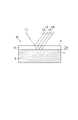
最初に、反射光による干渉を利用した膜厚測定の原理について説明する。図1に示す例では、膜状の測定対象物の一例として、基板2上に形成された半導体膜13を示している。このような膜厚dについて、基板2及び半導体膜13からなる試料12に対し、基板2とは反対側となる半導体膜13の上面(第1面)6側から膜厚測定用の照射光L1を供給する。そして、その上面6からの反射光L2と、下面(第2面、基板2と半導体膜13との境界面)7からの反射光L3〜Lmとが干渉して生成される干渉光を検出することで、半導体膜13の膜厚dを算出する。
First, the principle of film thickness measurement using interference by reflected light will be described. In the example shown in FIG. 1, a
次に、本発明に係る反射率測定装置を備えた膜厚測定装置の構成について説明する。図2は膜厚測定装置10の一実施形態の構成を示すブロック図である。図2では、試料測定部11の処理チャンバ内に設置された試料12の半導体膜13を測定対象物とした例を示している。膜厚測定装置10は、後述する反射率測定装置1と、測定光学系14と、膜厚算出部19とを備えている。
Next, the structure of the film thickness measuring apparatus provided with the reflectance measuring apparatus according to the present invention will be described. FIG. 2 is a block diagram showing a configuration of one embodiment of the film
膜厚算出部19は、測定対象物である半導体膜13の膜厚を算出する膜厚算出手段であり、反射率測定装置1から出力された波長毎の反射率(以下「波長毎の反射率」を「分光反射率データ」という)の算出値に基づいて膜厚を算出する。この膜厚算出部19の入力端は、反射率測定装置1の出力端と接続されている。なお、このような膜厚算出部19は、例えば所定の算出プログラムが実行されるコンピュータにより構成されることができる。
The film
この膜厚算出部19には、測定制御部20が接続されている。測定制御部20は、膜厚算出部19から出力される膜厚情報等を参照し、反射率測定装置1などの膜厚測定装置10の装置各部を制御することで、膜厚測定装置10における膜厚測定動作等の動作について必要な制御を行う。
A
この測定制御部20には、入力装置21及び表示装置22が接続されている。入力装置21は、反射率測定装置1及び膜厚測定装置10における測定動作に必要な情報、条件、指示等の操作者による入力に用いられる。また、表示装置22は、上記した測定動作についての必要な情報の操作者への表示に用いられる。
An
測定光学系14は、反射率測定装置1から供給される照射光L1を試料12の所定の測定位置に照射するとともに、試料12の表面で反射した反射光L2を反射率測定装置1に導光する。この測定光学系14に対して、反射率測定装置1からの照射光L1を導光する第1測定用光導波路(後述のため図示せず)、及び後述する試料12からの反射光L2を反射率測定装置1へと導光する第2測定用光導波路(後述のため図示せず)が光学的に結合されている。また測定光学系14には、内部に測定対象物である試料12が設置される試料測定部11が設けられている。この測定対象物には、波長毎の反射率が既知である基準測定対象物と、膜厚測定の対象となる測定対象物とがある。
The measurement
この測定光学系14には、XYθステージ15が設けられている。このXYθステージ15は、測定光学系14の位置、角度等をX方向、Y方向、θ方向に調整することで、膜厚測定装置10による半導体膜13での膜厚の測定位置、測定条件を調整する。また、XYθステージ15は、ステージ制御部16によって駆動制御されている。
The measurement
また、試料測定部11内の試料12、及び測定光学系14には、さらに撮像装置17、及び測定位置設定部18が設けられている。撮像装置17は、膜厚測定装置10による半導体膜13での膜厚の測定位置を確認するための位置確認用撮像装置である。また、測定位置設定部18は、撮像装置17によって測定光学系14を介して取得された半導体膜13を含む試料12の画像を参照して、試料12に対する膜厚測定位置を設定する。
The
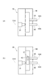
次に、第1実施形態に係る反射率測定装置1の構成について説明する。図3は、第1実施形態に係る反射率測定装置1の構成の一例を示す。この反射率測定装置1は、測定光源30、リファレンス用光導波路50、第1測定用光導波路60、第2測定用光導波路70、分光検出部80、及び処理部90を備えて構成されている。
Next, the configuration of the
この反射率測定装置1には、試料測定部11内の試料12の半導体膜13に対し、測定光学系14を介して照射光L1を供給する測定光源30が設けられている。この測定光源30は、所定帯域に亘る波長成分を少なくとも含む照射光L1を測定対象物である半導体膜13へと供給する。このような測定光源30としては、例えば、励起光及び励起光により生じた蛍光を含む光を照射する蛍光方式の白色発光ダイオード(LightEmittingDiode、以下「蛍光体方式の白色LED」という)を好適に用いることができる。白色LEDは、短波長の励起光が蛍光体に照射されることで長波長領域の蛍光が生成され、励起光と蛍光とが混合されて白色光を発生させるものである。なお、測定光源30としては、キセノンランプやハロゲンランプ等の光源や、赤色LED、緑色LED及び青色LEDなどを組み合わせた3色LED方式による白色LEDを用いてもよい。
The
第1測定用光導波路60は、測定光源30から測定光学系14へと照射光L1を導光する。この第1測定用光導波路60は、測定光源30から照射光L1が照射される照射光受光面61、及び測定対象物に照射光L1を供給する照射光供給面62を有している。照射光受光面61は測定光源30に光学的に結合され、照射光供給面62は測定光学系14に光学的に結合されている。この第1測定用光導波路60としては、例えば、光ファイバを好適に用いることができる。
The first measurement
第2測定用光導波路70は、試料12からの反射光L2を測定光学系14を介して反射率測定装置1へと導光する。この第2測定用光導波路70は、試料12からの反射光L2を受光する反射光受光面71を有している。反射光受光面71は、測定光学系14に光学的に結合されている。また、第2測定用光導波路70の他端は分光検出部80に光学的に結合されている。この第2測定用光導波路70としては、例えば、光ファイバを好適に用いることができる。
The second measurement
リファレンス用光導波路50の一端には、測定光源30から照射光L1が照射されるリファレンス光受光面51が設けられている。このリファレンス光受光面51は、測定光源30に光学的に結合されている。また、リファレンス用光導波路50の他端は分光検出部80に光学的に結合されている。このリファレンス用光導波路50としては、例えば、光ファイバを好適に用いることができる。
At one end of the reference
分光検出部80は、照射光L1の強度を波長毎に検出し、波長毎の強度の検出値(以下「波長毎の強度の検出値」を「スペクトル波形」という)を取得する第1検出部81、及び反射光L2のスペクトル波形を取得する第2検出部84を備えて構成されている。この第1検出部81は、分光光学系82及び光検出器83を備えて構成されている。分光光学系82は、分光光学系82に入射された光を波長毎に分解し、波長毎に分解した光を光検出器83に出力する。光検出器83は、分光光学系82から出力された光のスペクトル波形を取得し、取得したスペクトル波形を処理部90へ出力する。第1検出部81の分光光学系82の入力端には、リファレンス用光導波路50の他端が光学的に結合されている。また、光検出器83の出力端は処理部90の入力端に接続されている。また、第2検出部84も第1検出部81と同様に、分光光学系82及び光検出器83を備えて構成されている。第2検出部84の分光光学系82の入力端には第2測定用光導波路70の他端が光学的に結合されている。また、光検出器83の出力端は処理部90の他の入力端に接続されている。
The
処理部90は、係数算出部91、係数記録部92及び反射率算出部93を備えて構成されている。係数算出部91は、照射光L1のスペクトル波形を、基準測定対象物からの反射光L2のスペクトル波形に相当する値に変換する変換係数を算出する。係数記録部92は算出した変換係数を記録する。反射率算出部93は測定対象物の分光反射率データを算出する。処理部90の入力端は、第1検出部81の光検出器83の出力端と接続されている。また、処理部90の他の入力端は、第2検出部84の光検出器83の出力端と接続されている。さらに、処理部90の出力端は、図2に示す膜厚算出部19の入力端に接続されている。
The
係数算出部91は、基準測定対象物に照射される照射光L1のスペクトル波形と、基準測定対象物からの反射光L2のスペクトル波形とに基づいて変換係数を算出する。さらに、係数算出部91は、算出した変換係数を係数記録部92に出力する。この係数算出部91の出力端は、係数記録部92の入力端と接続されている。なお、このような係数算出部91は、例えば所定の算出プログラムが実行されるコンピュータにより構成されることができる。
The
係数記録部92は、上記した変換係数を記録し、該変換係数を反射率算出部93に出力する。この係数記録部92の入力端は、係数算出部91の出力端と接続されている。
The
反射率算出部93は、測定対象物に照射される照射光L1のスペクトル波形及び変換係数により求まる基準測定対象物からの反射光L2のスペクトル波形に相当する値と、測定対象物からの反射光L2のスペクトル波形とに基づいて、測定対象物の分光反射率データを算出し、算出したスペクトル波形を膜厚算出部19(図2参照)に出力する。この反射率算出部93の出力端は、膜厚算出部19(図2参照)の入力端と接続されている。なお、このような反射率算出部93は、例えば所定の算出プログラムが実行されるコンピュータにより構成されることができる。
The
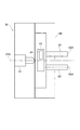
図4は、本実施形態における測定光源30、リファレンス用光導波路50、及び第1測定用光導波路60の構成を示す。この測定光源30は、蛍光体方式の白色LED31及び光源本体部32を備えて構成されている。また、リファレンス用光導波路50及び第1測定用光導波路60は光導波路保持部96により保持されている。本実施形態において、リファレンス用光導波路50及び第1測定用光導波路60は、リファレンス用光導波路50の中心軸50A及び第1測定用光導波路60の中心軸60Aが、白色LED31を通る軸31Aに対して互いに線対称となるように配置されている。
FIG. 4 shows the configuration of the
図5は、分光光学系82の構成の一例を示す。具体的には、分光光学系82は、照射光L1の測定対象物からの反射光L2と照射光L1とを、波長毎に検出可能なように分解する。この分光光学系82は、入射スリット301、コリメーティング光学系302、分散素子である回折格子303、及びフォーカシング光学系304を備えて構成されている。このような構成において、回折格子303で各波長へと分解された光は、フォーカシング光学系304を介して波長スペクトルの出力面305において波長成分毎に結像され、出力面305に配置された光検出器83によって波長成分毎に検出される。なお、本例以外にも、例えば帯域フィルタを用いることによって、測定対象物からの反射光L2と照射光L1とを波長毎に検出可能なように分解する分光光学系82を好適に構成することができる。
FIG. 5 shows an example of the configuration of the spectroscopic
図5に示すように、分光光学系82によって波長成分毎に分解された光に対し、各波長成分の強度を検出する検出手段として、光検出器83が設けられている。具体的には、この光検出器83は、分光光学系82によって分解された出力光の強度を数nm単位の波長成分毎に検出する。光検出器83は、例えば、図5に示した分光光学系82に対し、その出力面305に配置されて、分光光学系82によって分解された各波長成分の強度を検出する複数の光検出素子が配列されたマルチチャンネル光検出器により構成されている。
As shown in FIG. 5, a
次に、第1実施形態に係る反射率測定方法について説明する。説明の前に、ダーク減算補正について説明する。図3に示す第1検出部81からは、リファレンス用光導波路50から照射光L1の入射がない場合であっても微弱な信号が出力される。また、第2検出部84からは、第2測定用光導波路70から反射光L2の入射がない場合であっても微弱な信号が出力される。この微弱な信号は、暗電流と呼ばれるものである。この暗電流は、光検出素子により光の強度を取得する場合には校正を要する要素として扱う必要がある。この暗電流の他に、第1検出部81及び第2検出部84から出力される信号には、室内照明から照射される光等の外乱光に起因する信号が含まれている。上記した暗電流及び外乱光等の不要な信号を合わせたものをダーク信号と呼ぶことにする。照射光L1のスペクトル波形及び反射光L2のスペクトル波形を精度良く取得するためには、照射光L1のスペクトル波形及び反射光L2のスペクトル波形からダーク信号のスペクトル波形を減算する必要がある。
Next, the reflectance measurement method according to the first embodiment will be described. Before the description, dark subtraction correction will be described. A weak signal is output from the
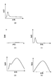
図6を参照しながら、ダーク減算補正の方法を説明する。ここでは、例として照射光L1についてダーク減算補正を行う方法について説明する。まず、測定光源30を消灯させて、分光検出部80によりダーク信号のスペクトル波形を取得する。図6(a)に示すように、ダーク信号のスペクトル波形は、白色雑音成分と特定の波長領域にピークを有する雑音成分とを含んでいる。白色雑音成分は、暗電流による雑音成分である(図6(b))。また、特定の波長領域において強度がピークを有する雑音成分は、外乱光等による雑音成分である(図6(c))。
A dark subtraction correction method will be described with reference to FIG. Here, as an example, a method of performing dark subtraction correction on the irradiation light L1 will be described. First, the
次に、測定光源30を点灯させて、分光検出部80により照射光L1のスペクトル波形を取得する。図6(d)に示すように、この光のスペクトル波形には照射光L1のスペクトル波形の成分ほかに、例えば図6(a)に示すようなダーク信号のスペクトル波形の成分が含まれている。そして、図6(d)に示すような照射光L1のスペクトル波形の成分及びダーク信号のスペクトル波形の成分を含んだスペクトル波形から、図6(a)に示すようなダーク信号のスペクトル波形を減算する。これにより、ダーク信号のスペクトル波形の成分を含まない、図6(e)に示すような照射光L1のスペクトル波形を精度良く取得することができる。反射光L2についても、測定光源30を点灯させて得た反射光L2のスペクトル波形から、測定光源30を消灯させて得たダーク信号のスペクトル波形を減算することにより、反射光L2のスペクトル波形を精度良く取得することができる。
Next, the
次に、ダーク減算補正を用いた本実施形態に係る反射率測定方法を説明する。図7及び図8は、第1実施形態に係る反射率測定方法を含む膜厚測定方法を示すフローチャートである。 Next, a reflectance measurement method according to this embodiment using dark subtraction correction will be described. 7 and 8 are flowcharts showing a film thickness measurement method including the reflectance measurement method according to the first embodiment.
まず、図7に示す変換係数K(λ)を算出する工程を実施する。ここでλは波長または分光検出部の波長分解単位を意味する。分光反射率データRref(λ)が既知である基準測定対象物を試料測定部11に設置する(S10)。次に、測定光源30を点灯させて、照射光L1を測定光源30からリファレンス光受光面51及び照射光受光面61へと照射させる。ここで、この変換係数K(λ)を算出する工程において、測定光源30から照射される照射光L1を補正用照射光と呼ぶことにする。照射光受光面61に照射された補正用照射光は、第1測定用光導波路60及び測定光学系14を介して、基準測定対象物へと供給される。(補正用照射光供給ステップS12)。
First, the step of calculating the conversion coefficient K (λ) shown in FIG. 7 is performed. Here, λ means the wavelength or the wavelength resolution unit of the spectroscopic detector. A reference measurement object whose spectral reflectance data Rref (λ) is known is set in the sample measurement unit 11 (S10). Next, the
リファレンス光受光面51に照射された補正用照射光は、リファレンス用光導波路50により第1検出部81に導光され、分光光学系82において波長成分毎に分解される。その後、光検出器83により補正用照射光のスペクトル波形Sref(λ)を取得する(補正用照射光検出ステップS14)。
The correction irradiation light irradiated to the reference
一方、基準測定対象物に供給された補正用照射光は、基準測定対象物の表面で反射し、反射光L2となる。ここで、基準測定対象物の表面で反射した補正用照射光を補正用反射光と呼ぶことにする。補正用反射光は、測定光学系14及び第2測定用光導波路70により第2検出部84に導光され、分光光学系82において波長成分毎に分解される。その後、光検出器83により補正用反射光のスペクトル波形Ssig(λ)を取得する(第1の反射光検出ステップS16)。次に、測定光源30を消灯させる(S18)。この状態において、第1検出部81から出力されるダーク信号のスペクトル波形Dref(λ)を取得する(S20)。さらに、第2検出部84から出力されるダーク信号のスペクトル波形Dsig(λ)を取得する(S22)。
On the other hand, the correction irradiation light supplied to the reference measurement object is reflected by the surface of the reference measurement object and becomes reflected light L2. Here, the correction irradiation light reflected by the surface of the reference measurement object is referred to as correction reflection light. The corrected reflected light is guided to the
下記の式(1)は変換係数K(λ)を算出する式である。基準測定対象物の分光反射率データRref(λ)、補正用照射光のスペクトル波形Sref(λ)、補正用反射光のスペクトル波形Ssig(λ)、第1検出部81から出力されるダーク信号のスペクトル波形Dref(λ)及び第2検出部84から出力されるダーク信号のスペクトル波形Dsig(λ)に基づいて、変換係数K(λ)を、算出する(係数算出ステップS24)。変換係数K(λ)の算出は、係数算出部91において実行される。変換係数K(λ)は係数記録部92に記録される(S26)。なお、上記した変換係数K(λ)を算出する工程は、出荷検査時若しくは定期的な保守作業で実施すれば足りる。
![]()
![]()
次に、図8に示す測定対象物の分光反射率データRsig(λ)を算出する工程を実施する。まず、測定対象物を試料測定部11に設置する(設置ステップS28)。次に、測定光源30を点灯させて、照射光L1をリファレンス光受光面51及び照射光受光面61に照射させる。ここで、この測定対象物の分光反射率データRsig(λ)を算出する場合において、測定光源30から照射される照射光L1を測定用照射光と呼ぶことにする。照射光受光面61に照射された測定用照射光は、第1測定用光導波路60及び測定光学系14を介して、測定対象物に供給される。(測定用照射光供給ステップS30)。
Next, a step of calculating spectral reflectance data Rsig (λ) of the measurement object shown in FIG. 8 is performed. First, a measurement object is installed in the sample measurement unit 11 (installation step S28). Next, the
リファレンス光受光面51に照射された測定用照射光は、リファレンス用光導波路50により第1検出部81に導光され、分光光学系82において波長成分毎に分解される。その後、光検出器83により測定用照射光のスペクトル波形S’ref(λ)を取得する(測定用照射光検出ステップS32)。測定用照射光のスペクトル波形S’ref(λ)を取得する時間を任意の時間に設定する。
The measurement irradiation light irradiated on the reference
一方、測定対象物に供給された測定用照射光は、測定対象物の表面で反射し、反射光L2となる。ここでは、反射光L2を測定用反射光と呼ぶことにする。測定用反射光は、測定光学系14及び第2測定用光導波路70により第2検出部84に導光され、分光光学系82において波長成分毎に分解される。その後、光検出器83により測定用反射光のスペクトル波形S’sig(λ)を取得する(第2の反射光検出ステップS34)。測定用反射光のスペクトル波形を取得する時間を任意の時間に設定する。
On the other hand, the measurement irradiation light supplied to the measurement object is reflected by the surface of the measurement object and becomes reflected light L2. Here, the reflected light L2 is referred to as measurement reflected light. The reflected light for measurement is guided to the
次に、測定光源30を消灯させる(S36)。測定光源30を消灯させる時間を100ミリ秒程度に設定する。その後、第1検出部81から出力されるダーク信号のスペクトル波形D’ref(λ)を取得する(S38)。ダーク信号のスペクトル波形D’ref(λ)を取得する時間を任意の時間に設定する。また、測定光源30を消灯させた状態で、第2検出部84から出力されるダーク信号のスペクトル波形D’sig(λ)を取得する(S40)。ダーク信号のスペクトル波形D’sig(λ)を取得する時間を任意の時間に設定する。
Next, the
下記の式(2)は、分光反射率データRsig(λ)を算出する数式である。式(2)の分子は、ダーク信号のスペクトル波形D’sig(λ)を含まない測定用反射光のスペクトル波形S’sig(λ)を示す。式(2)の分母は、基準測定対象物からの測定用反射光のスペクトル波形に相当する値を示す。測定用照射光のスペクトル波形S’ref(λ)からダーク信号のスペクトル波形D’ref(λ)を減算した波形と、変換係数K(λ)とを乗算することにより、式(2)の分母に該当する基準測定対象物からの測定用反射光のスペクトル波形に相当する値を算出する。そして、測定用反射光のスペクトル波形S’sig(λ)からダーク信号のスペクトル波形D’sig(λ)を減算した波形を、基準測定対象物からの測定用反射光のスペクトル波形に相当する値で除算することにより、測定対象物の分光反射率データRsig(λ)を算出する(反射率算出ステップS42)。分光反射率データRsig(λ)の算出は、反射率算出部93において実行される。
![]()
![]()
本実施形態における反射率測定装置1により測定された分光反射率データRsig(λ)は、膜厚算出部19に出力される。膜厚算出部19では、分光反射率データRsig(λ)に基づいて測定対象物の膜厚を算出する(S44)。
The spectral reflectance data Rsig (λ) measured by the
本実施形態による反射率測定装置1を用いた膜厚測定装置10、及び反射率測定方法を用いた膜厚測定方法ついて、はじめに測定光源30のスペクトル波形の変動に関する課題を説明しその後に作用効果を説明する。
Regarding the film
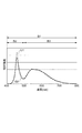
本実施形態による反射率測定装置1は、図4に示すように照射光L1の光源として蛍光体方式の白色LED31を備えている。一般的に、白色LED31では、周囲環境から与えられる熱のような外的要因により、励起光の光量が変動することが知られている。図9は、異なる温度環境下における白色LED31から発生させた白色光の波長と波長毎の相対強度との関係の一例を示すグラフである。この白色光が有する波長領域のうち、例えば、波長が400nm以上800nm以下である領域B1が、測定対象となる波長領域である。領域B1のうち例えば波長が400nm以上500nm以下である領域B2が励起光の波長領域であり、例えば波長が500nm以上800nm以下である領域B3が蛍光の波長領域である。また、図9の曲線G1は、室温の温度環境下で白色LED31を発光させた場合の白色光の波長毎の相対強度を示し、曲線G2は、0℃の温度環境下で白色LED31を発光させた場合の白色光の波長毎の相対強度を示す。図9の曲線G1と曲線G2とを比較すると、励起光の波長領域である領域B2において曲線G1と曲線G2とのピーク値が異なっている。すなわち、異なる温度環境下で白色LED31を発光させた場合には、励起光の波長領域における相対強度が相違する。
The
この励起光の波長領域の強度の相違は、白色LED31を照明器具に用いる場合には問題とならない。一方、白色LED31を、測定光の波長領域に励起光の波長領域が含まれるような測定に用いる場合には問題となる。なお、蛍光の波長領域である領域B3において曲線G1と曲線G2とでは、相対強度の相違は殆どない。これは、蛍光体が飽和状態になるように、蛍光体に励起光を供給しているためである。
This difference in intensity in the wavelength region of the excitation light does not cause a problem when the
上記に例示したように、測定光源30が備える白色LED31から照射される照射光L1のスペクトル波形は、周囲温度等の外的要因により変動する。例えば、基準測定対象物からの反射光L2のスペクトル波形を取得する際の白色LED31の温度と、測定対象物からの反射光L2のスペクトル波形を取得する際の白色LED31の温度とが相違した場合は、基準測定対象物に照射された補正用照射光と、測定対象物に照射された測定用照射光との励起光の波長領域における波長毎の相対強度が相違する。そのために、測定対象物の分光反射率データRsig(λ)を精度良く測定できない。
As illustrated above, the spectrum waveform of the irradiation light L1 emitted from the
本実施形態による反射率測定装置1及び反射率測定方法によれば、基準測定対象物からの測定用反射光のスペクトル波形に相当する値を、測定対象物の測定の際に基準測定対象物を用いることなく、測定対象物に照射される測定用照射光のスペクトル波形S’ref(λ)と、変換係数K(λ)とから測定毎に算出することができる。これにより、測定対象物の分光反射率データRsig(λ)を算出する際には、照射光L1の変動の影響を含んだ測定用反射光のスペクトル波形に相当する値を用いることができる。すなわち、測定用照射光のスペクトル波形S’ref(λ)が変動する場合であっても、測定用反射光のスペクトル波形S’sig(λ)に含まれる測定用照射光のスペクトル波形S’ref(λ)の変動をキャンセルすることが可能となる。従って、測定対象物の分光反射率データRsig(λ)を常に精度良く測定することができる。なお、変換係数K(λ)は、スペクトル波形S’ref(λ)が変動しても影響を受けることはない。
According to the
さらに、本実施形態による反射率測定装置を備える膜厚測定装置10、及び本実施形態による反射率測定方法を含む膜厚測定方法によれば、測定対象物の分光反射率データRsig(λ)を精度良く算出することが可能となるため、分光反射率データRsig(λ)から求まる測定対象物の膜厚を精度良く算出することができる。
Furthermore, according to the film
また、精度の良い分光反射率データRsig(λ)が得られることにより、同一の測定対象物について複数回の反射率測定をした場合に得られる分光反射率データRsig(λ)のばらつきを抑えることができる。従って、分光反射率データRsig(λ)から算出される測定対象物の膜厚の測定値のばらつきを抑えることができる。 In addition, by obtaining accurate spectral reflectance data Rsig (λ), it is possible to suppress variations in spectral reflectance data Rsig (λ) obtained when the same measurement object is subjected to reflectance measurement multiple times. Can do. Therefore, it is possible to suppress variations in the measured value of the film thickness of the measurement object calculated from the spectral reflectance data Rsig (λ).
また、照射光L1のスペクトル波形の変動があるような場合、生産現場においては、基準測定対象物を用いて基準測定対象物からの測定用反射光のスペクトル波形を測定毎に取得し、取得したスペクトル波形を再度設定していた。これによれば、基準測定対象物からの測定用反射光のスペクトル波形を取得し、再度設定するために、生産ラインを一時停止させる必要がある。そのために、生産ラインにおける生産効率を低下させる要因となっていた。 Further, when there is a change in the spectrum waveform of the irradiation light L1, in the production site, the spectrum waveform of the reflected light for measurement from the reference measurement object is acquired for each measurement using the reference measurement object, and acquired. The spectrum waveform was set again. According to this, it is necessary to temporarily stop the production line in order to acquire and set the spectrum waveform of the reflected light for measurement from the reference measurement object. For this reason, it has been a factor of reducing the production efficiency in the production line.
本実施形態による反射率測定装置1及び反射率測定方法によれば、基準測定対象物からの測定用反射光のスペクトル波形に相当する値を測定用照射光のスペクトル波形S’ref(λ)及び変換係数K(λ)から算出する。従って、基準測定対象物からの測定用反射光のスペクトル波形を測定毎に取得することなく、分光反射率データRsig(λ)を算出することが可能となる。これにより、照射光L1のスペクトル波形の変動があるような場合であっても、基準測定対象物からの測定用反射光のスペクトル波形に相当する値を取得する工程を測定毎に実施することなく、分光反射率データRsig(λ)を精度良く測定することができる。さらに、作業工程を削減することができるため、生産効率の低下を防ぐことができ、コストダウンが可能となる。
According to the
次に、図10及び図11を参照しながらリファレンス用光導波路50及び第1測定用光導波路60と、白色LED31を含む測定光源30との位置関係により、スペクトル波形が異なる課題について述べ、その後作用効果を説明する。図10(a)は、白色LED31を通る軸31Aと光導波路P1の中心軸P1Aとを一致させて、白色LED31と光導波路P1とを対向させた位置に光導波路P1を配置した形態を示している。図10(b)は、白色LED31を通る軸31Aと光導波路P2の中心軸P2Aとを離間させた位置に光導波路P2を配置した形態を示している。図10(c)は、白色LED31を通る軸31Aと光導波路P3の中心軸P3Aとをさらに離間させた位置に光導波路P2を配置した形態を示している。
Next, with reference to FIG. 10 and FIG. 11, problems with different spectral waveforms depending on the positional relationship between the reference
図11は、図10に示す光導波路P1〜P3に入射された照射光L1の波長毎の相対強度を示すグラフである。図9と同様に、B1は測定対象となる波長領域であり、B2は励起光の波長領域であり、B3は蛍光の波長領域である。また、曲線G3は光導波路P1に入射された照射光L1の波長毎の相対強度であり、曲線G4は光導波路P2に入射された照射光L1の波長毎の相対強度であり、曲線G5は光導波路P3に入射された照射光L1の波長毎の相対強度である。 FIG. 11 is a graph showing the relative intensity for each wavelength of the irradiation light L1 incident on the optical waveguides P1 to P3 shown in FIG. Similarly to FIG. 9, B1 is a wavelength region to be measured, B2 is a wavelength region of excitation light, and B3 is a wavelength region of fluorescence. The curve G3 is the relative intensity for each wavelength of the irradiation light L1 incident on the optical waveguide P1, the curve G4 is the relative intensity for each wavelength of the irradiation light L1 incident on the optical waveguide P2, and the curve G5 is the light intensity. It is the relative intensity for each wavelength of the irradiation light L1 incident on the waveguide P3.
図11に示すように、それぞれの光導波路P1〜P3に入射された照射光L1の波長毎の相対強度は、蛍光の波長領域(B3)では略同じである。一方、励起光の波長領域(B2)ではピーク値が相違する。すなわち、リファレンス用光導波路50及び第1測定用光導波路60と、白色LED31との位置関係により、励起光の波長領域においてスペクトル波形が相違する。
As shown in FIG. 11, the relative intensity for each wavelength of the irradiation light L1 incident on each of the optical waveguides P1 to P3 is substantially the same in the fluorescence wavelength region (B3). On the other hand, the peak values are different in the wavelength region (B2) of the excitation light. That is, the spectral waveform differs in the wavelength region of the excitation light depending on the positional relationship between the reference
蛍光体方式の白色LED31の場合、発光素子からの光が励起光となり蛍光体に照射されることで蛍光を生じる。図12は、照射光L1の照射範囲の断面を示す概念図である。励起光は指向性があるために、照射光L1の照射範囲の断面における中心部T1は励起光の影響が強い領域となる。また、蛍光は広域性があるため、照射光L1の照射範囲の断面における周辺部T2は蛍光の影響が強い領域となる。そのため、測定光源30と光導波路P1〜P3との位置関係により、光導波路P1〜P3に入射させた照射光L1のスペクトル波形が異なると考えられる。
In the case of the phosphor type
本実施形態による反射率測定装置1を用いた膜厚測定装置10では、図4に示すようにリファレンス用光導波路50及び第1測定用光導波路60は、リファレンス用光導波路50の中心軸50A及び第1測定用光導波路60の中心軸60Aが、白色LED31を通る軸31Aに対して互いに線対称となるように配置されている。
In the film
図13は、このように配置した場合に、リファレンス用光導波路50及び第1測定用光導波路60に照射される照射光L1の波長毎の相対強度を示す。図9と同様に、B1は測定対象となる波長領域であり、B2は励起光の波長領域であり、B3は蛍光の波長領域である。曲線G6はリファレンス用光導波路50に照射された射光L1の波長毎の相対強度を示し、曲線G7は第1測定用光導波路60に照射された射光L1の波長毎の相対強度を示す。リファレンス用光導波路50の中心軸50A及び第1測定用光導波路60の中心軸60Aが、白色LED31を通る軸31Aに対して互いに線対称となるように配置された場合には、リファレンス用光導波路50及び第1測定用光導波路60に照射される照射光L1のスペクトル波形の違いが抑制されている。従って、本実施形態による反射率測定装置1を用いた膜厚測定装置10によれば、リファレンス用光導波路50に照射される照射光L1のスペクトル波形と、第1測定用光導波路60に照射される照射光L1のスペクトル波形との違いを抑制し、分光反射率データRsig(λ)を精度の良く測定することができる。
FIG. 13 shows the relative intensity for each wavelength of the irradiation light L <b> 1 irradiated to the reference
また、本実施形態による反射率測定装置1は、測定光源30として白色LED31を備えている。白色LED31の寿命は、従来に使用されていた寿命が1000時間程度であるキセノンランプやハロゲンランプ等のランプ系光源よりも長い。これにより、測定光源30が備えている光源の交換回数を減少させることができる。
Further, the
また、本実施形態による反射率測定装置1は、リファレンス用光導波路50及び第1測定用光導波路60を備える。このような構成によれば、それぞれの光導波路の配置を調整することが可能となる。これにより、リファレンス用光導波路50及び第1測定用光導波路60に照射される照射光L1の波長毎の強度を調整することができる。
The
また、本実施形態による反射率測定装置1は、分光検出部80が第1検出部81及び第2検出部84を備えている。このような構成によれば、照射光L1のスペクトル波形を取得する検出部及び測定対象物からの反射光L2のスペクトル波形を取得する検出部を互いに独立させることができる。従って、照射光L1のスペクトル波形及び測定対象物からの反射光L2のスペクトル波形を同時に取得することが可能となり、さらに測定対象物の分光反射率データRsig(λ)を精度良く測定することができる。さらに、波長毎の反射率の測定に要する時間を短縮することができる。
Further, in the
また、本実施形態による反射率測定装置1は、上記した式(2)により分光反射率データRsig(λ)を算出する。式(2)を用いることにより、分光反射率データRsig(λ)を容易に算出することができる。さらに、式(2)によれば基準測定対象物の分光反射率データRref(λ)を用いることなく分光反射率データRsig(λ)を算出できる。従って、基準測定対象物の分光反射率データRref(λ)を記録する装置を備えることなく、反射率測定装置1を構成することができる。
(第2実施形態)
Further, the
(Second Embodiment)
続いて、第2実施形態について説明する。図14は、第2実施形態に係る反射率測定装置1Aの構成の一例を示す。図14に示される本実施形態と、上記した第1実施形態とで異なる点は、複数の試料12を同時に測定することができるように構成されている点である。すなわち、本実施形態による反射率測定装置1Aは、第1測定用光導波路60、測定光学系14、第2測定用光導波路70、第2検出部84をそれぞれ複数備えて構成されている。ここで、本実施形態では2つの試料12についてそれぞれの分光反射率データRsig(n、λ)を算出する場合を例に説明する。なお、本実施形態による反射率測定装置1Aによれば試料12は2つ以上であってもよい。
Next, the second embodiment will be described. FIG. 14 shows an example of the configuration of the
次に、本実施形態に係る反射率測定装置1Aの構成について説明する。なお、ここでは第1実施形態と異なる構成となる点についてのみ説明をする。この反射率測定装置1Aは、測定光源30、リファレンス用光導波路50、2つの第1測定用光導波路60、2つの第2測定用光導波路70、分光検出部80A、及び処理部90を備えて構成されている。
Next, the configuration of the
本実施形態に係る分光検出部80Aは、照射光L1のスペクトル波形を取得する第1検出部81、及び試料12A、12Bからの反射光L2のスペクトル波形を取得する2つの第2検出部84を備えて構成されている。一方の第2検出部84の分光光学系82には、試料12A、12Bのいずれか一方からの反射光L2を導光する第2測定用光導波路70の他端が光学的に結合されている。また、他方の第2検出部84の分光光学系82には、試料12A、12Bの他方からの反射光L2を導光する第2測定用光導波路70の他端が光学的に結合されている。
The
測定光源30から照射された照射光L1は、第1測定用光導波路60及び測定光学系14を介して試料12A、12Bに供給される。試料12A、12Bに供給された照射光L1は試料12A、12Bの表面で反射し、反射光L2となる。反射光L2は測定光学系14及び第2測定用光導波路70を介して第2の検出部84の分光光学系82に供給される。分光光学系82に供給された反射光L2は、波長毎に検出可能なように分解される。その後、光検出器83により反射光L2のスペクトル波形を取得する。
Irradiation light L1 emitted from the
次に、ダーク減算補正を用いた本実施形態に係る反射率測定方法について説明する。なお、ダーク減算補正の原理は、第1実施形態で説明した原理と同じである。本実施形態と第1実施形態とで相違する点は、第1実施形態では1つの変換係数K(λ)を算出したが、本実施形態では第2検出部84毎に変換係数K(n、λ)を算出する点が相違する。ここでnは、本実施形態ではn=1〜2の整数である。また、本実施形態では複数の試料12毎に分光反射率データRsig(n、λ)を算出する点が第1実施形態と相違する。本実施形態に係る反射率測定方法の手順において上記した相違点以外の手順は、第1実施形態と同様である。
Next, a reflectance measurement method according to this embodiment using dark subtraction correction will be described. The principle of dark subtraction correction is the same as that described in the first embodiment. The difference between this embodiment and the first embodiment is that one conversion coefficient K (λ) is calculated in the first embodiment, but in this embodiment, the conversion coefficient K (n, The difference is that λ) is calculated. Here, n is an integer of n = 1 to 2 in the present embodiment. Further, the present embodiment is different from the first embodiment in that the spectral reflectance data Rsig (n, λ) is calculated for each of the plurality of
まず、本実施形態では、2つの第2検出部84のそれぞれについて変換係数K(n、λ)を算出する。下記の式(3)は変換係数K(n、λ)を算出する式である。基準測定対象物からの補正用反射光のスペクトル波形Ssin(n、λ)、補正用照射光のスペクトル波形Sref(λ)、ダーク信号のスペクトル波形Dsig(n、λ)、Dref(λ)、及び基準測定対象物の既知の分光反射率Rref(λ)に基づいて、変換係数K(n、λ)を算出する。
![]()
![]()
次に、試料12A、12Bの分光反射率データRsig(n、λ)を算出する。下記の式(4)は分光反射率データRsig(n、λ)を算出する式である。測定対象物からの測定用反射光のスペクトル波形S’sin(n、λ)、測定用照射光のスペクトル波形S’ref(λ)、ダーク信号のスペクトル波形D’sig(n、λ)、D’ref(λ)、及び変換係数K(n、λ)に基づいて、試料12A、12Bの分光反射率データRsig(n、λ)を算出する。
![]()
![]()
本実施形態の反射率測定装置1A及び反射率測定装置1Aを用いた反射率測定方法によれば、複数の測定対象物の分光反射率データRsig(n、λ)を測定することができる。また、複数の測定対象物の分光反射率データRsig(n、λ)を同時に測定することもできる。さらに、本実施形態の反射率測定装置1Aを備える膜厚測定装置10、及び膜厚装置10を用いた膜厚測定方法によれば、複数の測定対象物の膜厚を同時に測定することができる。
(第3実施形態)
According to the
(Third embodiment)
続いて、第3実施形態について説明する。図15は、第3実施形態に係る反射率測定装置1Bの構成の一例を示す。上記した第1実施形態と本実施形態とで異なる点は、図15に示すように、分光検出部80Bが第3の検出部85により構成されている点である。すなわち、本実施形態においては、第3検出部85により照射光L1のスペクトル波形及び反射光L2のスペクトル波形が取得される構成が第1実施形態と異なっている。さらに、上記した第1実施形態と本実施形態とで異なる点は、本実施形態に係る反射率測定装置1Bが光導波路選択手段40を備えている点である。なお、分光検出部80B及び光導波路選択手段40以外の装置構成については、第1実施形態と同様である。
Subsequently, the third embodiment will be described. FIG. 15 shows an example of the configuration of the
まず、図15に示すような本実施形態に用いられる反射率測定装置1Bの構成について説明する。なお、ここでは第1実施形態と異なる構成となる点についてのみ説明をする。測定光源30には光導波路選択手段40が光学的に結合されている。この光導波路選択手段40は、シャッタ41を含んで構成されている。シャッタ41により、リファレンス用光導波路50及び第1測定用光導波路60の少なくとも一方に、選択的に照射光L1を照射することができる。また、リファレンス用光導波路50及び第1測定用光導波路60の双方に照射しないようにすることもできる。
First, the configuration of the
リファレンス用光導波路50において、リファレンス光受光面51が設けられた一端は光導波路選択手段40と光学的に結合されており、他端は第3検出部85における分光光学系82に光学的に結合されている。第1測定用光導波路60において、照射光受光面61が設けられた一端は光導波路選択手段40と光学的に結合されている。また、第2測定用光導波路70において他端は第3検出部85における分光光学系82に光学的に結合されている。
In the reference
次に、ダーク減算補正を用いた第3実施形態に係る反射率測定方法について説明する。図16及び図17は本実施形態に係る反射率測定方法を含む膜厚測定方法を示すフローチャートである。なお、ダーク減算補正の原理は、第1実施形態で説明した原理と同じである。 Next, a reflectance measurement method according to the third embodiment using dark subtraction correction will be described. 16 and 17 are flowcharts showing a film thickness measuring method including the reflectance measuring method according to the present embodiment. The principle of dark subtraction correction is the same as that described in the first embodiment.
まず、図16に示す変換係数K(λ)を算出する工程を実施する。本実施形態では変換係数K(λ)を算出する方法として、測定光源30を制御してダーク信号のスペクトル波形を取得することにより変換係数K(λ)を算出する方法を説明する。
First, the step of calculating the conversion coefficient K (λ) shown in FIG. 16 is performed. In this embodiment, as a method for calculating the conversion coefficient K (λ), a method for calculating the conversion coefficient K (λ) by controlling the
分光反射率データRref(λ)が既知である基準測定対象物を試料測定部11に設置する(S50)。次に、光導波路選択手段40を制御して、照射光受光面61への照射光L1の照射を遮断しリファレンス光受光面51のみに照射光L1を入射させるようにシャッタ41を操作する(S52)。シャッタ41を操作する時間は100ミリ秒程度かかる。次に、測定光源30を点灯させて、照射光L1を測定光源30からリファレンス光受光面51へと照射させる。(S54)。ここで、この変換係数K(λ)を算出する工程において測定光源30から照射される照射光L1を補正用照射光と呼ぶことにする。
A reference measurement object whose spectral reflectance data Rref (λ) is known is set in the sample measurement unit 11 (S50). Next, the optical waveguide selection means 40 is controlled to operate the
リファレンス光受光面51に照射された補正用照射光は、リファレンス用光導波路50により第3検出部85に導光される。第3検出部85に導光された補正用照射光は、分光光学系82において波長成分毎に分解される。その後、光検出器83により補正用照射光のスペクトル波形Sref(λ)を取得する(補正用照射光検出ステップS56)。なお、補正用照射光のスペクトル波形Sref(λ)を取得する時間は任意の時間に設定される。次に、測定光源30を消灯させる(S58)。測定光源30を消灯させる時間は補正用照射光のスペクトル波形Sref(λ)を取得する時間と同程度の時間に設定される。その後、第3検出部85から出力されるダーク信号のスペクトル波形Dref(λ)を取得する(S60)。
The correction irradiation light irradiated on the reference
次に、光導波路選択手段40を制御して、リファレンス光受光面51への補正用照射光の照射を遮断し、照射光受光面61のみに補正用照射光が照射されるようにシャッタ41を操作する(S62)。シャッタ41を操作する時間は100ミリ秒程度かかる。この状態において、第3検出部85から出力されるダーク信号のスペクトル波形Dsig(λ)を取得する(S64)。ダーク信号のスペクトル波形Dsig(λ)を取得する時間は補正用反射光のスペクトル波形Ssig(λ)を取得する時間と同程度の時間に設定される。なお、ここでは上記したDref(λ)をDsig(λ)として用いてもよい。
Next, the optical waveguide selection means 40 is controlled to block the irradiation of the correction irradiation light on the reference
次に、測定光源30を点灯させる。照射光受光面61に照射される補正用照射光は、第1測定用光導波路60及び測定光学系14を介して、基準測定対象物に供給される(補正用照射光供給ステップS66)。基準測定対象物に供給された補正用照射光は、基準測定対象物の表面で反射し、反射光L2となる。ここで、反射光L2を補正用反射光と呼ぶことにする。補正用反射光は、測定光学系14及び第2測定用光導波路70により第3検出部85に導光され、分光光学系82において波長成分毎に分解される。その後、光検出器83により補正用反射光のスペクトル波形Ssig(λ)を取得する(第1の反射光検出ステップS68)。補正用反射光のスペクトル波形Ssig(λ)を取得する時間は、所定の時間に設定される。
Next, the
下記の式(5)は変換係数K(λ)を算出する式である。基準測定対象物の分光反射率データRref(λ)、補正用照射光のスペクトル波形Sref(λ)、補正用反射光のスペクトル波形Ssig(λ)、第3検出部85から出力されるダーク信号のスペクトル波形Dref(λ)、Dsig(λ)に基づいて、変換係数K(λ)を算出する(係数算出ステップS70)。変換係数K(λ)の算出は、係数算出部91において実行される。変換係数K(λ)は係数記録部92に記録される(S72)。なお、上記した変換係数K(λ)を算出する工程は、出荷検査時若しくは定期的な保守作業で実施すれば足りる。
![]()
![]()
次に、図17に示す測定対象物の分光反射率データRsig(λ)を算出する工程を実施する。まず、測定対象物を試料測定部11に設置する(設置ステップS74)。次に、光導波路選択手段40を制御して、リファレンス光受光面51に測定光源30からの照射光L1を入射させるように、シャッタ41を操作する(S76)。次に、測定光源30を点灯させて、照射光L1をリファレンス光受光面51に照射させる。(S78)。ここで、この測定対象物の分光反射率データRsig(λ)を算出する場合において、測定光源30から照射される照射光L1を測定用照射光と呼ぶことにする。
Next, a step of calculating spectral reflectance data Rsig (λ) of the measurement object shown in FIG. 17 is performed. First, a measurement object is installed in the sample measurement unit 11 (installation step S74). Next, the optical waveguide selection means 40 is controlled to operate the
リファレンス光受光面51に照射された測定用照射光は、リファレンス用光導波路50を介して第3検出部85に供給される。第3検出部85に供給された測定用照射光は、分光光学系82において波長成分毎に分解される。その後、光検出器83により測定用照射光のスペクトル波形S’ref(λ)を取得する(測定用照射光検出ステップS80)。
The measurement irradiation light irradiated on the reference
次に、測定光源30を消灯させる(S82)。この状態において、第3検出部85から出力されるダーク信号のスペクトル波形D’ref(λ)を取得する(S84)。次に、第3検出部85から出力されるダーク信号のスペクトル波形D’sig(λ)を取得する(S86)。なお、上記したD’ref(λ)及びD’sig(λ)のうちD’ref(λ)のみを取得し、取得されたD’ref(λ)をD’sig(λ)として用いてもよい。逆に、上記したD’ref(λ)及びD’sig(λ)のうちD’sig(λ)のみを取得し、取得したD’sig(λ)をD’ref(λ)として用いてもよい。
Next, the
次に、光導波路選択手段40を制御して、リファレンス光受光面51への測定用照射光の照射を遮断し照射光受光面61のみに測定用照射光が照射されるようにシャッタ41を操作する(S88)。次に、測定光源30を点灯させる。照射光受光面61に照射された測定用照射光は、第1測定用光導波路60及び測定光学系14を介して、測定対象物に供給される(測定用照射光供給ステップS90)。
Next, the optical waveguide selection means 40 is controlled to operate the
測定用対象物に供給された測定用照射光は、測定対象物の表面で反射し、反射光L2となる。ここでは、反射光L2を測定用反射光と呼ぶことにする。測定用反射光は、測定光学系14及び第2測定用光導波路70により第3検出部85に導光され、分光光学系82において波長成分毎に分解される。その後、光検出器83により測定用反射光のスペクトル波形S’sig(λ)を取得する(第2の反射光検出ステップS92)。
The measurement irradiation light supplied to the measurement object is reflected by the surface of the measurement object and becomes reflected light L2. Here, the reflected light L2 is referred to as measurement reflected light. The reflected light for measurement is guided to the
下記の式(6)は、分光反射率データRsig(λ)を算出する数式である。測定用照射光のスペクトル波形S’ref(λ)、ダーク信号のスペクトル波形D’ref(λ)、及び変換係数K(λ)に基づいて、式(6)の分母に該当する基準測定対象物からの測定用反射光のスペクトル波形に相当する値を算出する。そして、測定用反射光のスペクトル波形S’sig(λ)、ダーク信号のスペクトル波形D’sig(λ)、及び式(6)の分母に該当する基準測定対象物からの測定用反射光のスペクトル波形に相当する値に基づいて、測定対象物の分光反射率データRsig(λ)を算出する(反射率算出ステップS94)。分光反射率データRsig(λ)の算出は、反射率算出部93において実行される。
![]()
![]()
本実施形態における反射率測定装置1Bにより測定された分光反射率データRsig(λ)は、膜厚算出部19に出力される。膜厚算出部19では、分光反射率データRsig(λ)に基づいて測定対象物の膜厚を算出する(S96)。
The spectral reflectance data Rsig (λ) measured by the
本実施形態による反射率測定装置1及び反射率測定方法によれば、上記した第1実施形態と同様に、基準測定対象物からの測定用反射光のスペクトル波形S’sig(λ)に相当する値を、測定対象物に照射される測定用照射光のスペクトル波形S’ref(λ)と、係数記録部92に記録された変換係数K(λ)とから測定毎に算出することができる。これにより、測定用照射光のスペクトル波形S’ref(λ)が変動する場合であっても、測定対象物からの測定用反射光のスペクトル波形S’sig(λ)に含まれる測定用照射光のスペクトル波形S’ref(λ)の変動の影響をキャンセルすることが可能となる。従って、測定対象物の分光反射率データRsig(λ)を精度良く測定することができる。
According to the
本実施形態による反射率測定装置1Bによれば、分光検出部80Bは1つの光検出器83により構成することが可能となる。この構成により、反射率測定装置1Bの構成を簡素にし、小型化することができる。さらに、反射率測定装置1Bの構成を簡素にすることにより製造に必要な部材及び製造工程を削減することが可能となるため、反射率測定装置1Bの製造コストを抑制することができる。
(第4実施形態)
According to the
(Fourth embodiment)
続いて、第3実施形態の変形例である第4実施形態について説明する。上記した第3実施形態と本実施形態とで異なる点は、変換係数K(λ)を算出する方法である。第3実施形態では、測定光源30を制御することにより変換係数K(λ)を算出したが、本実施形態では測定光源30は点灯させた状態にし、光導波路選択手段40を制御することにより変換係数K(λ)を算出している。なお、本実施形態に使用する反射率測定装置1Bは、第3実施形態に使用する反射率測定装置1Bと同様の構成を備える。また、分光反射率データRsig(λ)に基づいて測定対象物の膜厚等を算出する図17に示す工程は、第3実施形態の工程と同様である。
Then, 4th Embodiment which is a modification of 3rd Embodiment is described. The difference between the third embodiment and the present embodiment is a method of calculating the conversion coefficient K (λ). In the third embodiment, the conversion coefficient K (λ) is calculated by controlling the
図18に示す変換係数K(λ)を算出する工程について説明する。本実施形態では、変換係数K(λ)を算出する方法として、光導波路選択手段40を制御してダーク信号のスペクトル波形を取得することにより変換係数K(λ)を算出する方法を説明する。
A process of calculating the conversion coefficient K (λ) shown in FIG. 18 will be described. In the present embodiment, as a method for calculating the conversion coefficient K (λ), a method for calculating the conversion coefficient K (λ) by controlling the optical
分光反射率データRref(λ)が既知である基準測定対象物を試料測定部11に設置する(S100)。次に、光導波路選択手段40を制御して、照射光受光面61への照射光L1の照射を遮断しリファレンス光受光面51のみに照射光L1を照射するようにシャッタ41を操作する(S102)。次に、測定光源30を点灯させる(S104)。ここで、この変換係数K(λ)を算出する工程において測定光源30から照射される照射光L1を補正用照射光と呼ぶことにする。
A reference measurement object whose spectral reflectance data Rref (λ) is known is set in the sample measurement unit 11 (S100). Next, the optical waveguide selection means 40 is controlled to operate the
リファレンス光受光面51に照射された補正用照射光は、リファレンス用光導波路50により第3検出部85に導光される。第3検出部85に導光された補正用照射光は、分光光学系82において波長成分毎に分解される。その後、光検出器83により補正用照射光のスペクトル波形Sref(λ)を取得する(補正用照射光検出ステップS106)。補正用照射光のスペクトル波形Sref(λ)を取得する時間を任意の時間に設定する。
The correction irradiation light irradiated on the reference
次に、光導波路選択手段40を制御して、リファレンス光受光面51及び照射光受光面61に補正用照射光が照射されないようにシャッタ41を操作する(S108)。その後、第3検出部85から出力されるダーク信号のスペクトル波形Dref(λ)を取得する(S110)。ダーク信号のスペクトル波形Dref(λ)を取得する時間を補正用照射光のスペクトル波形Sref(λ)を取得する時間と同程度に設定する。さらに、第3検出部85から出力されるダーク信号のスペクトル波形Dsig(λ)を取得する(S112)。なお、Dref(λ)及びDsig(λ)は同時に測定してもよい。次に、光導波路選択手段40を制御して、照射光受光面61に補正用照射光が照射されるようにシャッタ41を操作する。照射光受光面61に照射された補正用照射光は、第1測定用光導波路60及び測定光学系14を介して、基準測定対象物に供給される(補正用照射光供給ステップS114)。
Next, the optical waveguide selection means 40 is controlled to operate the
基準測定対象物に供給された補正用照射光は、基準測定対象物の表面で反射し、反射光L2となる。ここでは、反射光L2を補正用反射光と呼ぶことにする。補正用反射光は、測定光学系14及び第2測定用光導波路70により第3検出部85に導光される。第3検出部85に導光された補正用反射光は、分光光学系82において波長成分毎に分解される。その後、光検出器83により補正用反射光のスペクトル波形Ssig(λ)を取得する(第1の反射検出ステップS116)。補正用反射光スペクトル波形の取得する時間を任意の時間に設定する。
The correction irradiation light supplied to the reference measurement object is reflected by the surface of the reference measurement object and becomes reflected light L2. Here, the reflected light L2 is referred to as correction reflected light. The corrected reflected light is guided to the
下記の式(7)は変換係数K(λ)を算出する式である。基準測定対象物の分光反射率データRref(λ)、補正用照射光のスペクトル波形Sref(λ)、補正用反射光のスペクトル波形Ssig(λ)、第3検出部85から出力されるダーク信号のスペクトル波形Dref(λ)、Dsig(λ)に基づいて、変換係数K(λ)を算出する(係数算出ステップS118)。変換係数K(λ)の算出は、係数算出部91において実行される。変換係数K(λ)は係数記録部92に記録される(S120)。なお、上記した変換係数K(λ)を算出する工程は、出荷検査時若しくは定期的な保守作業で実施すれば足りる。
![]()
![]()
光導波路選択手段40を制御することにより変換係数K(λ)を算出する上記した方法によれば、測定光源30を連続して点灯させた状態で基準測定対象物の分光反射率データRref(λ)、補正用照射光のスペクトル波形Sref(λ)、補正用反射光のスペクトル波形Ssig(λ)、第3検出部85から出力されるダーク信号のスペクトル波形Dref(λ)、Dsig(λ)を取得することが可能である。そのため、測定光源30を連続して点灯させた状態で変換係数K(λ)を算出することができる。従って、測定の間は測定光源30を点灯させた状態を維持することが可能となり、測定光源30から照射される照射光L1のスペクトル波形を安定させることができる。
According to the above-described method of calculating the conversion coefficient K (λ) by controlling the optical waveguide selection means 40, the spectral reflectance data Rref (λ of the reference measurement object with the
本発明による反射率測定装置及び反射率測定方法は、上記実施形態に限られるものではなく、様々な変形が可能である。例えば、上記した第1実施形態及び第2実施形態では、図19に示すように、リファレンス用光導波路50及び第1測定用光導波路60はバンドルファイバ95を介して測定光源30と光学的に結合されていてもよい。リファレンス用光導波路50及び第1測定用光導波路60は、リファレンス光受光面51及び照射光受光面61を介してバンドルファイバ95の一端に光学的に結合されている。リファレンス用光導波路50の中心軸50Aと第1測定用光導波路60の中心軸60Aとは、バンドルファイバ95の中心軸95Aに対して互いに線対称となるように配置されている。このバンドルファイバ95は光導波路保持部96により保持され、白色LED31の中心を通る軸と、バンドルファイバ95の中心軸95Aとが略一致するように光学的に結合されている。
The reflectance measuring device and the reflectance measuring method according to the present invention are not limited to the above-described embodiments, and various modifications are possible. For example, in the first and second embodiments described above, the reference
図19に示す構成を備えた反射率測定装置1によれば、白色LED31を通る軸31Aと、リファレンス用光導波路50の中心軸50A及び第1測定用光導波路60の中心軸60Aとの位置の調整を容易に行うことができる。
According to the
また、バンドルファイバ95により光導波路を分岐させる場合は、バンドルファイバ95を構成するファイバを理想的なランダム配置にすることが望まれる。バンドルファイバ95を構成するファイバを理想的なランダム配置にすることが製造上の問題により困難である場合には、バンドルファイバ95を用いることなく反射率測定装置1を構成することもできる。バンドルファイバ95を用いない構成にすることにより、反射率測定装置1の製造コストを抑制することができる。
In addition, when the optical waveguide is branched by the
また、リファレンス用光導波路50に入射される照射光L1、及び第1測定用光導波路60に入射される照射光L1の光量の大きさを調整する必要がある場合は、バンドルファイバ95を用いることなく反射率測定装置1を構成することもできる。バンドルファイバ95を用いない構成にすることにより、リファレンス用光導波路50に入射される照射光L1、及び第1測定用光導波路60に入射される照射光L1の光量の大きさを調整することができる。
In addition, when it is necessary to adjust the amount of light of the irradiation light L1 incident on the reference
さらに、図20はバンドルファイバ95を備えた反射率測定装置1の他の変形例の構成を示す。図19の変形例と相違する点は、光導波路選択手段40を備えている点である。光導波路選択手段40を備えていることにより、リファレンス用光導波路50及び第1測定用光導波路60の少なくとも一方について選択的に、白色LED31から照射された照射光L1を照射することができる。また、リファレンス用光導波路50及び第1測定用光導波路60の双方に照射しないようにすることもできる。
Furthermore, FIG. 20 shows a configuration of another modified example of the
また、図20に示す構成を備えた反射率測定装置1では、反射率測定装置1の構成が煩雑になる場合がある。簡易な構成による反射率測定装置1を望む場合には、バンドルファイバ95を用いることなく反射率測定装置1を構成することもできる。バンドルファイバ95を用いない構成にすることにより、測定光源30と光導波路選択手段40とを備える構成を簡素にすることができる。さらに簡素な構成にすることにより、測定光源30と光導波路選択手段40とを容易に一体化することができる。さらに、測定光源30と光導波路選択手段40とを備える構成を容易に小型化することができる。
Further, in the
また、上記した第1実施形態〜第4実施形態では、リファレンス用光導波路50及び第1測定用光導波路60は、リファレンス用光導波路50の中心軸50A及び第1測定用光導波路60の中心軸60Aが、白色LED31を通る軸31Aに対して互いに線対称となるように配置されているが、図21(a)に示すように白色LED31と第1測定用光導波路60とが対向するように配置されていてもよい。これによれば、試料12に供給される照射光L1の光量を大きくすることができる。従って、照射光L1、反射光L2が光導波路等を通過することにより減衰した場合であっても、分光反射率データRsig(λ)を精度良く測定するために必要な光量を確保することができる。また、図21(b)のように、光導波路選択手段40を備えていてもよい。
In the first to fourth embodiments described above, the reference
また、上記した第1実施形態に示した反射利率測定装置1及び第2実施形態に示した反射利率測定装置1Aでは、光導波路選択手段40を備えていないが、図22に示すように光導波路選択手段40を備えていても良い。
In addition, the reflection
また、上記した第1実施形態〜第4実施形態では、照射光L1のスペクトル波形Sref(λ)と、ダーク減算補正用の補正データであるDsig(λ)、Dref(λ)とを測定毎に取得する必要がある。本発明による反射率測定装置及び反射率測定方法はこれに限られるものではなく、例えば、一連の測定時間内において照射光L1のスペクトル波形Sref(λ)及びダーク信号のスペクトル波形Dsig(λ)、Dref(λ)の変動が測定結果に影響を及ぼさない程度であれば、照射光L1のスペクトル波形Sref(λ)及びダーク信号のスペクトル波形Dsig(λ)、Dref(λ)の取得は測定開始直後に1回のみ実施して該データを保存しておき、それ以降は保存されたデータを使用してもよい。これにより、タクトタイムを短縮することができる。 In the first to fourth embodiments described above, the spectral waveform Sref (λ) of the irradiation light L1 and the Dsig (λ) and Dref (λ) that are correction data for dark subtraction correction are measured for each measurement. Need to get. The reflectance measuring apparatus and the reflectance measuring method according to the present invention are not limited to this. For example, the spectral waveform Sref (λ) of the irradiation light L1 and the spectral waveform Dsig (λ) of the dark signal within a series of measurement times. If the fluctuation of Dref (λ) does not affect the measurement result, the spectral waveform Sref (λ) of the irradiation light L1 and the spectral waveforms Dsig (λ) and Dref (λ) of the dark signal are acquired immediately after the start of measurement The data may be stored only once, and the stored data may be used thereafter. Thereby, the tact time can be shortened.
また、上記した第1実施形態〜第4実施形態では、反射率測定装置1を、分光反射率データの算出値に基づいて膜厚を算出する膜厚測定装置10に用いている。本発明による反射率測定装置1はこれに限られるものではなく、分光反射率データの算出値に基づいて、色を測定する色測定装置、反射率を測定する反射率測定装置、または透過率を測定する透過率測定装置に用いてもよい。
In the first to fourth embodiments described above, the
また、上記した第1実施形態、第3実施形態、及び第4実施形態では下記に示す式(8)を用いて変換係数K(λ)を算出し、さらに式(9)を用いて分光反射率データRsig(λ)を算出している。本発明による反射率測定装置1はこれに限られるものではなく、下記に示す式(10)を用いて変換係数K(λ)を算出し、さらに式(11)を用いて分光反射率データRsig(λ)を算出してもよい。

1…反射率測定装置、30…測定光源、80…分光検出部、92…係数記録部、93…反射率算出部、L1…照射光、L2…反射光、K(λ)…変換係数。
DESCRIPTION OF
Claims (11)
前記照射光の強度及び前記測定対象物からの反射光の強度を波長毎に検出する分光検出部と、
前記照射光の波長毎の強度の検出値を、基準測定対象物からの反射光の波長毎の強度に相当する値に変換するための変換係数を記録する係数記録部と、
前記照射光の波長毎の強度の検出値及び前記変換係数より求まる前記基準測定対象物からの前記反射光の波長毎の強度に相当する値に基づいて、前記測定対象物の波長毎の反射率を算出する反射率算出部と、
を備えることを特徴とする反射率測定装置。 A measurement light source for supplying irradiation light to a measurement object;
A spectroscopic detector that detects the intensity of the irradiation light and the intensity of reflected light from the measurement object for each wavelength;
A coefficient recording unit for recording a conversion coefficient for converting the detected value of the intensity for each wavelength of the irradiation light into a value corresponding to the intensity for each wavelength of the reflected light from the reference measurement object;
Based on a value corresponding to the intensity for each wavelength of the reflected light from the reference measurement object obtained from the detected value of the intensity for each wavelength of the irradiation light and the conversion coefficient, the reflectance for each wavelength of the measurement object. A reflectance calculation unit for calculating
A reflectance measuring device comprising:
前記測定光源から前記照射光が照射される照射光受光面を一端に有し、前記測定対象物へ前記照射光を供給する照射光供給面を他端に有する第1測定用光導波路と、
前記測定対象物からの前記反射光を受光する反射光受光面を一端に有し、他端が前記分光検出部に光学的に結合されている第2測定用光導波路と、
をさらに備えることを特徴とする請求項1又は2のいずれか一項に記載の反射率測定装置。 A reference optical waveguide having a reference light receiving surface irradiated with the irradiation light from the measurement light source at one end and the other end optically coupled to the spectral detection unit,
A first optical waveguide for measurement having an irradiation light receiving surface irradiated with the irradiation light from the measurement light source at one end and an irradiation light supply surface for supplying the irradiation light to the measurement object at the other end;
A second optical waveguide for measurement having a reflected light receiving surface for receiving the reflected light from the measurement object at one end and the other end optically coupled to the spectroscopic detection unit;
The reflectance measuring device according to claim 1, further comprising:
前記リファレンス用光導波路の他端は、前記第1検出部に光学的に結合され、前記第2測定用光導波路の他端は、前記第2検出部に光学的に結合されていることを特徴とする請求項3に記載の反射率測定装置。 The spectral detection unit has a first detection unit that detects the intensity of the irradiation light for each wavelength, and a second detection unit that detects the intensity of the reflected light from the measurement object for each wavelength,
The other end of the reference optical waveguide is optically coupled to the first detection unit, and the other end of the second measurement optical waveguide is optically coupled to the second detection unit. The reflectance measuring apparatus according to claim 3.
前記分光検出部は、前記照射光の強度を波長毎に検出し且つ前記反射光の強度を波長毎に検出する第3検出部を有し、
前記リファレンス用光導波路の他端と前記第2測定用光導波路の他端とは、前記第3検出部に光学的に結合されていることを特徴とする請求項3に記載の反射率測定装置。 Optical waveguide selection means for selectively making the irradiation light emitted from the measurement light source selectively enter one of the reference light receiving surface and the irradiation light receiving surface;
The spectral detection unit includes a third detection unit that detects the intensity of the irradiation light for each wavelength and detects the intensity of the reflected light for each wavelength;
The reflectance measuring apparatus according to claim 3, wherein the other end of the reference optical waveguide and the other end of the second measurement optical waveguide are optically coupled to the third detection unit. .
前記補正用照射光を測定光源から前記基準測定対象物へと供給する補正用照射光供給ステップと、
前記基準測定対象物からの前記補正用照射光の反射光の強度を波長毎に検出する第1の反射光検出ステップと、
前記補正用照射光検出ステップにより得られる前記補正用照射光の波長毎の強度の検出値と、前記第1の反射光検出ステップにより得られる前記補正用照射光の反射光の波長毎の強度の検出値とに基づいて、測定対象物へと供給される測定用照射光の波長毎の強度の検出値を、前記基準測定対象物からの前記測定用照射光の反射光の波長毎の強度に相当する値に変換するための変換係数を算出する係数算出ステップと、
前記測定対象物を設置する設置ステップと、
励起光及び前記励起光により生じた蛍光を含む前記測定用照射光の強度を波長毎に検出する測定用照射光検出ステップと、
前記測定用照射光を前記測定光源から前記測定対象物へと供給する測定用照射光供給ステップと、
前記測定対象物からの前記測定用照射光の反射光の強度を波長毎に検出する第2の反射光検出ステップと、
前記測定用照射光検出ステップにより得られる前記測定用照射光の波長毎の強度の検出値及び前記変換係数により求まる前記基準測定対象物からの前記測定用照射光の反射光の波長毎の強度に相当する値と、前記第2の反射光検出ステップにより得られる前記測定対象物からの前記測定用照射光の反射光の波長毎の強度の検出値とに基づいて、前記測定対象物の波長毎の反射率を算出する反射率算出ステップとを備えることを特徴とする反射率測定方法。 A correction irradiation light detection step for detecting, for each wavelength, the intensity of the correction irradiation light supplied to the reference measurement object;
A correction irradiation light supply step of supplying the correction irradiation light from a measurement light source to the reference measurement object;
A first reflected light detection step for detecting, for each wavelength, the intensity of reflected light of the correction irradiation light from the reference measurement object;
The detection value of the intensity for each wavelength of the correction irradiation light obtained by the correction irradiation light detection step and the intensity for each wavelength of the reflection light of the correction irradiation light obtained by the first reflected light detection step. Based on the detection value, the detection value of the intensity for each wavelength of the measurement irradiation light supplied to the measurement object is changed to the intensity for each wavelength of the reflected light of the measurement irradiation light from the reference measurement object. A coefficient calculating step for calculating a conversion coefficient for conversion into a corresponding value;
An installation step of installing the measurement object;
A measurement irradiation light detection step for detecting, for each wavelength, the intensity of the measurement irradiation light including excitation light and fluorescence generated by the excitation light;
A measurement irradiation light supply step for supplying the measurement irradiation light from the measurement light source to the measurement object;
A second reflected light detection step for detecting the intensity of the reflected light of the measurement irradiation light from the measurement object for each wavelength;
Intensity for each wavelength of reflected light of the measurement irradiation light from the reference measurement object obtained from the detection value of the intensity of the measurement irradiation light for each wavelength obtained by the measurement irradiation light detection step and the conversion coefficient Based on the corresponding value and the detected value of the intensity for each wavelength of the reflected light of the measurement irradiation light from the measurement object obtained by the second reflected light detection step, for each wavelength of the measurement object And a reflectance calculating step for calculating the reflectance of the reflectance.
A film thickness measuring method comprising the reflectance measuring method according to claim 10, wherein the film thickness of the measurement object is calculated based on a reflectance for each wavelength obtained by the reflectance measuring method.
Priority Applications (7)
| Application Number | Priority Date | Filing Date | Title |
|---|---|---|---|
| JP2010209668A JP2012063321A (en) | 2010-09-17 | 2010-09-17 | Reflectivity measurement device, reflectivity measurement method, film thickness measurement device, and film thickness measurement method |
| US13/822,741 US8699023B2 (en) | 2010-09-17 | 2011-09-14 | Reflectivity measuring device, reflectivity measuring method, membrane thickness measuring device, and membrane thickness measuring method |
| DE112011103113.0T DE112011103113B4 (en) | 2010-09-17 | 2011-09-14 | Reflectivity measurement method, membrane thickness measurement device and membrane thickness measurement method |
| PCT/JP2011/071020 WO2012036213A1 (en) | 2010-09-17 | 2011-09-14 | Reflectivity measuring device, reflectivity measuring method, membrane thickness measuring device, and membrane thickness measuring method |
| CN201180044880.7A CN103140750B (en) | 2010-09-17 | 2011-09-14 | Reflectivity measuring device, reflectivity measuring method, membrane thickness measuring device, and membrane thickness measuring method |
| KR1020137003557A KR20130106810A (en) | 2010-09-17 | 2011-09-14 | Reflectivity measuring device, reflectivity measuring method, membrane thickness measuring device, and membrane thickness measuring method |
| TW100133490A TWI513972B (en) | 2010-09-17 | 2011-09-16 | Reflectance measuring apparatus reflectivity measurement method, film thickness measuring apparatus and method for measuring film thickness |
Applications Claiming Priority (1)
| Application Number | Priority Date | Filing Date | Title |
|---|---|---|---|
| JP2010209668A JP2012063321A (en) | 2010-09-17 | 2010-09-17 | Reflectivity measurement device, reflectivity measurement method, film thickness measurement device, and film thickness measurement method |
Publications (2)
| Publication Number | Publication Date |
|---|---|
| JP2012063321A true JP2012063321A (en) | 2012-03-29 |
| JP2012063321A5 JP2012063321A5 (en) | 2013-10-03 |
Family
ID=45831669
Family Applications (1)
| Application Number | Title | Priority Date | Filing Date |
|---|---|---|---|
| JP2010209668A Pending JP2012063321A (en) | 2010-09-17 | 2010-09-17 | Reflectivity measurement device, reflectivity measurement method, film thickness measurement device, and film thickness measurement method |
Country Status (7)
| Country | Link |
|---|---|
| US (1) | US8699023B2 (en) |
| JP (1) | JP2012063321A (en) |
| KR (1) | KR20130106810A (en) |
| CN (1) | CN103140750B (en) |
| DE (1) | DE112011103113B4 (en) |
| TW (1) | TWI513972B (en) |
| WO (1) | WO2012036213A1 (en) |
Cited By (6)
| Publication number | Priority date | Publication date | Assignee | Title |
|---|---|---|---|---|
| WO2013146163A1 (en) * | 2012-03-29 | 2013-10-03 | 住友化学株式会社 | Polarizing plate fabrication method and fabrication apparatus |
| JP2016510408A (en) * | 2013-01-31 | 2016-04-07 | ベンタナ メディカル システムズ, インコーポレイテッド | System and method for calibrating, configuring, and determining validity of an imaging device or system for multiple tissue assays |
| JP2020020815A (en) * | 2019-11-06 | 2020-02-06 | 株式会社キーエンス | Confocal displacement meter |
| JP2021067557A (en) * | 2019-10-24 | 2021-04-30 | 大塚電子株式会社 | Optical measurement device and optical measurement method |
| US20220065697A1 (en) * | 2020-08-26 | 2022-03-03 | Yokogawa Electric Corporation | Spectroscopic analysis device, optical system, and method |
| KR20230063313A (en) | 2021-11-01 | 2023-05-09 | 캐논 톡키 가부시키가이샤 | Reflectivity measuring device, film forming apparatus |
Families Citing this family (12)
| Publication number | Priority date | Publication date | Assignee | Title |
|---|---|---|---|---|
| WO2014038090A1 (en) * | 2012-09-10 | 2014-03-13 | 株式会社シンクロン | Measuring apparatus and film-forming apparatus |
| CN105745526B (en) * | 2014-01-09 | 2018-11-30 | 夏普株式会社 | Light intensity sensing device and detection method |
| JPWO2016181743A1 (en) * | 2015-05-12 | 2018-03-01 | コニカミノルタ株式会社 | Plant growth index measuring apparatus and method, and plant growth index measuring system |
| JP6248244B1 (en) * | 2016-08-09 | 2017-12-20 | ナルックス株式会社 | Parts with position measuring unit |
| JP6533770B2 (en) * | 2016-11-10 | 2019-06-19 | 日東電工株式会社 | A reference device, a spectral interference type measuring device, a coating apparatus, a method for guaranteeing measurement accuracy of the spectral interference type measuring device, and a method of manufacturing a coated film. |
| JP7076951B2 (en) * | 2017-05-23 | 2022-05-30 | 株式会社ディスコ | Reflectance detector |
| JP7092146B2 (en) * | 2017-11-01 | 2022-06-28 | コニカミノルタ株式会社 | Film thickness measurement method, film thickness measurement system, light reflection film manufacturing method and light reflection film manufacturing system |
| CN110806388B (en) * | 2019-11-20 | 2022-05-27 | 河南牧业经济学院 | Dark light column positioning device, positioning method and color measurement method of columnar laser paper |
| CN113646874B (en) * | 2020-03-11 | 2023-07-28 | 株式会社日立高新技术 | Plasma processing apparatus and plasma processing method |
| GB202009640D0 (en) | 2020-06-24 | 2020-08-05 | Ams Sensors Singapore Pte Ltd | Optical detection system calibration |
| KR20230125053A (en) * | 2020-12-30 | 2023-08-28 | 주식회사 씨젠 | Method and device for detecting target analyte in spectroscopic analysis-based sample |
| CN113720825B (en) * | 2021-11-04 | 2022-02-08 | 四川丹诺迪科技有限公司 | Optical instant detector and detection method and application |
Citations (2)
| Publication number | Priority date | Publication date | Assignee | Title |
|---|---|---|---|---|
| JPH01308930A (en) * | 1988-06-08 | 1989-12-13 | Dainippon Screen Mfg Co Ltd | Microspectroscopic apparatus |
| JP2006132986A (en) * | 2004-11-02 | 2006-05-25 | Olympus Corp | Optical biological information measuring instrument and measuring method using it |
Family Cites Families (21)
| Publication number | Priority date | Publication date | Assignee | Title |
|---|---|---|---|---|
| JPH0820223B2 (en) | 1990-03-20 | 1996-03-04 | 日本航空電子工業株式会社 | Method and apparatus for measuring film thickness / refractive index |
| JP2698286B2 (en) | 1992-05-22 | 1998-01-19 | 大日本スクリーン製造株式会社 | Surface treatment end point detector |
| FR2693565B1 (en) | 1992-07-10 | 1994-09-23 | France Telecom | Method for adjusting a photolithographic exposure machine and associated device. |
| JP3219223B2 (en) | 1993-08-12 | 2001-10-15 | 株式会社日立製作所 | Characteristic value measuring method and device |
| JP3106790B2 (en) * | 1993-09-01 | 2000-11-06 | 株式会社日立製作所 | Thin film characteristic value measuring method and apparatus |
| JPH10123250A (en) | 1996-10-24 | 1998-05-15 | Nec Corp | Electronic distance measuring system and method |
| JPH1196333A (en) * | 1997-09-16 | 1999-04-09 | Olympus Optical Co Ltd | Color image processor |
| JP2000193424A (en) | 1998-12-24 | 2000-07-14 | Sharp Corp | Method and device for measuring thickness of thin-film |
| JP2000212773A (en) * | 1999-01-20 | 2000-08-02 | Hamamatsu Photonics Kk | Wet etching completion point detecting device |
| US6504301B1 (en) * | 1999-09-03 | 2003-01-07 | Lumileds Lighting, U.S., Llc | Non-incandescent lightbulb package using light emitting diodes |
| JP2001267300A (en) | 2000-03-21 | 2001-09-28 | Olympus Optical Co Ltd | Measuring method and apparatus of etching depth |
| JP3995579B2 (en) * | 2002-10-18 | 2007-10-24 | 大日本スクリーン製造株式会社 | Film thickness measuring device and reflectance measuring device |
| JP2005084019A (en) * | 2003-09-11 | 2005-03-31 | Akifumi Ito | Temperature measuring method of substrate |
| JP4216209B2 (en) * | 2004-03-04 | 2009-01-28 | 大日本スクリーン製造株式会社 | Film thickness measuring method and apparatus |
| JP2007212260A (en) * | 2006-02-09 | 2007-08-23 | Mitsubishi Electric Corp | Reflectance measuring device, reflectance measuring method, and manufacturing method of display panel |
| JP4687644B2 (en) | 2006-12-22 | 2011-05-25 | 富士ゼロックス株式会社 | Image processing apparatus, image reading apparatus, and image forming apparatus |
| JP5090837B2 (en) * | 2007-09-19 | 2012-12-05 | 浜松ホトニクス株式会社 | Spectrometer, spectroscopic method, and spectroscopic program |
| KR100947464B1 (en) * | 2008-02-13 | 2010-03-17 | 에스엔유 프리시젼 주식회사 | Apparatus for measuring thickness |
| JP5274862B2 (en) | 2008-03-10 | 2013-08-28 | 東京エレクトロン株式会社 | Temperature measuring apparatus and temperature measuring method |
| JP5410806B2 (en) | 2009-03-27 | 2014-02-05 | 浜松ホトニクス株式会社 | Film thickness measuring apparatus and measuring method |
| US8885173B2 (en) | 2009-10-13 | 2014-11-11 | Hamamatsu Photonics K.K. | Film thickness measurement device and film thickness measurement method |
-
2010
- 2010-09-17 JP JP2010209668A patent/JP2012063321A/en active Pending
-
2011
- 2011-09-14 CN CN201180044880.7A patent/CN103140750B/en active Active
- 2011-09-14 US US13/822,741 patent/US8699023B2/en active Active
- 2011-09-14 DE DE112011103113.0T patent/DE112011103113B4/en active Active
- 2011-09-14 KR KR1020137003557A patent/KR20130106810A/en not_active Application Discontinuation
- 2011-09-14 WO PCT/JP2011/071020 patent/WO2012036213A1/en active Application Filing
- 2011-09-16 TW TW100133490A patent/TWI513972B/en active
Patent Citations (2)
| Publication number | Priority date | Publication date | Assignee | Title |
|---|---|---|---|---|
| JPH01308930A (en) * | 1988-06-08 | 1989-12-13 | Dainippon Screen Mfg Co Ltd | Microspectroscopic apparatus |
| JP2006132986A (en) * | 2004-11-02 | 2006-05-25 | Olympus Corp | Optical biological information measuring instrument and measuring method using it |
Cited By (11)
| Publication number | Priority date | Publication date | Assignee | Title |
|---|---|---|---|---|
| WO2013146163A1 (en) * | 2012-03-29 | 2013-10-03 | 住友化学株式会社 | Polarizing plate fabrication method and fabrication apparatus |
| JP2016510408A (en) * | 2013-01-31 | 2016-04-07 | ベンタナ メディカル システムズ, インコーポレイテッド | System and method for calibrating, configuring, and determining validity of an imaging device or system for multiple tissue assays |
| US10012537B2 (en) | 2013-01-31 | 2018-07-03 | Ventana Medical Systems, Inc. | Systems and methods for calibrating, configuring and validating an imaging device or system for multiplex tissue assays |
| US10598548B2 (en) | 2013-01-31 | 2020-03-24 | Ventana Medical Systems, Inc. | Systems and methods for calibrating, configuring and validating an imaging device or system for multiplex tissue assays |
| US11566941B2 (en) | 2013-01-31 | 2023-01-31 | Ventana Medical Systems, Inc. | Systems and methods for calibrating, configuring and validating an imaging device or system for multiplex tissue assays |
| JP2021067557A (en) * | 2019-10-24 | 2021-04-30 | 大塚電子株式会社 | Optical measurement device and optical measurement method |
| JP7341849B2 (en) | 2019-10-24 | 2023-09-11 | 大塚電子株式会社 | Optical measurement device and optical measurement method |
| JP2020020815A (en) * | 2019-11-06 | 2020-02-06 | 株式会社キーエンス | Confocal displacement meter |
| US20220065697A1 (en) * | 2020-08-26 | 2022-03-03 | Yokogawa Electric Corporation | Spectroscopic analysis device, optical system, and method |
| US11940326B2 (en) * | 2020-08-26 | 2024-03-26 | Yokogawa Electric Corporation | Spectroscopic analysis device, optical system, and method |
| KR20230063313A (en) | 2021-11-01 | 2023-05-09 | 캐논 톡키 가부시키가이샤 | Reflectivity measuring device, film forming apparatus |
Also Published As
| Publication number | Publication date |
|---|---|
| CN103140750B (en) | 2015-06-03 |
| DE112011103113T5 (en) | 2013-08-08 |
| DE112011103113B4 (en) | 2022-11-10 |
| KR20130106810A (en) | 2013-09-30 |
| TWI513972B (en) | 2015-12-21 |
| US8699023B2 (en) | 2014-04-15 |
| TW201224430A (en) | 2012-06-16 |
| WO2012036213A1 (en) | 2012-03-22 |
| CN103140750A (en) | 2013-06-05 |
| US20130169968A1 (en) | 2013-07-04 |
Similar Documents
| Publication | Publication Date | Title |
|---|---|---|
| WO2012036213A1 (en) | Reflectivity measuring device, reflectivity measuring method, membrane thickness measuring device, and membrane thickness measuring method | |
| US10267622B2 (en) | Confocal displacement sensor | |
| TWI480501B (en) | Displacement measurement method and displacement measuring device | |
| JP7408265B2 (en) | confocal displacement meter | |
| KR101548017B1 (en) | Apparatus for measuring optical property | |
| CN104568155A (en) | Spectroscopic measurement device and spectroscopic measurement method | |
| KR20060041959A (en) | Film thickness measuring method and apparatus | |
| US8049882B2 (en) | Spectrometric optical method and system providing required signal-to-noise of measurements | |
| KR101890944B1 (en) | Spectral characteristic measurement method and spectral characteristic measurement apparatus | |
| JP2007139632A (en) | Reflectivity measuring instrument and reflectivity measuring method | |
| JP5338467B2 (en) | Plasma measuring device | |
| JP2017207354A (en) | Light source device | |
| CN114688964B (en) | Critical dimension measurement correction method, system and computer readable storage medium | |
| US20230058064A1 (en) | Film thickness measuring device and film thickness measuring method | |
| JPH11153416A (en) | Film thickness measuring device, and film thickness measuring method | |
| JP2010190729A (en) | Spectral sensitivity characteristic measuring device and spectral sensitivity characteristic measuring method | |
| JP2012018118A (en) | Colorimetric device and colorimetric method | |
| JP5216657B2 (en) | Optical film thickness measuring apparatus and vacuum film forming apparatus having the same | |
| US20240069316A1 (en) | Microscope and imaging method for a microscope | |
| JP7136136B2 (en) | Light-receiving characteristic evaluation device and light-receiving characteristic evaluation method for optical sensor | |
| EP4141477A1 (en) | Imaging lidar apparatus and methods for operation in day-light conditions | |
| JP6928688B2 (en) | Confocal displacement meter | |
| JP2019002721A (en) | Confocal displacement meter | |
| JP2017203722A (en) | Light source device | |
| JPH06331320A (en) | Film thickness measuring device |
Legal Events
| Date | Code | Title | Description |
|---|---|---|---|
| A521 | Request for written amendment filed |
Free format text: JAPANESE INTERMEDIATE CODE: A523 Effective date: 20130819 |
|
| A621 | Written request for application examination |
Free format text: JAPANESE INTERMEDIATE CODE: A621 Effective date: 20130819 |
|
| A131 | Notification of reasons for refusal |
Free format text: JAPANESE INTERMEDIATE CODE: A131 Effective date: 20140930 |
|
| A521 | Request for written amendment filed |
Free format text: JAPANESE INTERMEDIATE CODE: A523 Effective date: 20141128 |
|
| A131 | Notification of reasons for refusal |
Free format text: JAPANESE INTERMEDIATE CODE: A131 Effective date: 20150127 |
|
| A02 | Decision of refusal |
Free format text: JAPANESE INTERMEDIATE CODE: A02 Effective date: 20150602 |