JP5113573B2 - LED lighting device - Google Patents
LED lighting device Download PDFInfo
- Publication number
- JP5113573B2 JP5113573B2 JP2008076699A JP2008076699A JP5113573B2 JP 5113573 B2 JP5113573 B2 JP 5113573B2 JP 2008076699 A JP2008076699 A JP 2008076699A JP 2008076699 A JP2008076699 A JP 2008076699A JP 5113573 B2 JP5113573 B2 JP 5113573B2
- Authority
- JP
- Japan
- Prior art keywords
- light
- light source
- opening
- full
- esushito
- Prior art date
- Legal status (The legal status is an assumption and is not a legal conclusion. Google has not performed a legal analysis and makes no representation as to the accuracy of the status listed.)
- Active
Links
Images


Classifications
-
- F—MECHANICAL ENGINEERING; LIGHTING; HEATING; WEAPONS; BLASTING
- F21—LIGHTING
- F21V—FUNCTIONAL FEATURES OR DETAILS OF LIGHTING DEVICES OR SYSTEMS THEREOF; STRUCTURAL COMBINATIONS OF LIGHTING DEVICES WITH OTHER ARTICLES, NOT OTHERWISE PROVIDED FOR
- F21V13/00—Producing particular characteristics or distribution of the light emitted by means of a combination of elements specified in two or more of main groups F21V1/00 - F21V11/00
- F21V13/02—Combinations of only two kinds of elements
-
- F—MECHANICAL ENGINEERING; LIGHTING; HEATING; WEAPONS; BLASTING
- F21—LIGHTING
- F21V—FUNCTIONAL FEATURES OR DETAILS OF LIGHTING DEVICES OR SYSTEMS THEREOF; STRUCTURAL COMBINATIONS OF LIGHTING DEVICES WITH OTHER ARTICLES, NOT OTHERWISE PROVIDED FOR
- F21V11/00—Screens not covered by groups F21V1/00, F21V3/00, F21V7/00 or F21V9/00
- F21V11/08—Screens not covered by groups F21V1/00, F21V3/00, F21V7/00 or F21V9/00 using diaphragms containing one or more apertures
- F21V11/14—Screens not covered by groups F21V1/00, F21V3/00, F21V7/00 or F21V9/00 using diaphragms containing one or more apertures with many small apertures
-
- F—MECHANICAL ENGINEERING; LIGHTING; HEATING; WEAPONS; BLASTING
- F21—LIGHTING
- F21V—FUNCTIONAL FEATURES OR DETAILS OF LIGHTING DEVICES OR SYSTEMS THEREOF; STRUCTURAL COMBINATIONS OF LIGHTING DEVICES WITH OTHER ARTICLES, NOT OTHERWISE PROVIDED FOR
- F21V3/00—Globes; Bowls; Cover glasses
-
- F—MECHANICAL ENGINEERING; LIGHTING; HEATING; WEAPONS; BLASTING
- F21—LIGHTING
- F21Y—INDEXING SCHEME ASSOCIATED WITH SUBCLASSES F21K, F21L, F21S and F21V, RELATING TO THE FORM OR THE KIND OF THE LIGHT SOURCES OR OF THE COLOUR OF THE LIGHT EMITTED
- F21Y2115/00—Light-generating elements of semiconductor light sources
- F21Y2115/10—Light-emitting diodes [LED]
Landscapes
- Engineering & Computer Science (AREA)
- General Engineering & Computer Science (AREA)
- Planar Illumination Modules (AREA)
- Led Device Packages (AREA)
Description
本発明は、発光波長の異なる複数のLEDチップを有する光源を利用したLED照明装置に関するものである。 The present invention relates to an LED illumination device using a light source having a plurality of LED chips having different emission wavelengths.
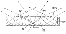
従来から、この種のLED照明装置として、図9に示すように、一面開口した箱状に形成されたケース100と、ケース100の底壁の中央部に形成された窓孔101内に配置され発光波長の異なる複数のLEDチップ(例えば、赤色LEDチップ、緑色LEDチップ、青色LEDチップ)を有する光源1’と、透光性材料(例えば、アクリル樹脂、シリコーン樹脂などのポリマー)により形成されケース100内に収納された導光体102と、導光体102におけるケース100の底壁側とは反対の放射面102a側に形成され光源1’からの光を所定の割合で反射させる放射側反射部103と、導光体102とケース100の内面との間に設けられ光源1’から放射され放射側反射部103で反射された光を反射する内側反射部104とを備えたものが提案されている(特許文献1)。
ところで、図9に示した構成のLED照明装置では、導光体102での光損失に起因して光取出し効率が低下してしまう。また、図9に示した構成のLED照明装置では、光源1’が1種類のLEDチップのみを利用したものであれば、大面積で均一な照明光を得ることが可能であるが、導光体102の放射面102a側の放射側反射部103が光源1’からの光を所定の割合で反射させるように形成されており、光源1’からの光の一部が放射側反射部103で反射されずに直接外部へ出射されるので(なお、図9中に一点鎖線で示した矢印は、光源1’から放射された光の伝搬経路を示している)、光源1’において発光波長の異なる複数のLEDチップが近接配置されていても、光源1’自体に色むらがある場合、LED照明装置全体として色むらが発生してしまう。
By the way, in the LED illumination device having the configuration shown in FIG. 9, the light extraction efficiency is reduced due to the light loss in the
本発明は上記事由に鑑みて為されたものであり、その目的は、光取出し効率を向上でき且つ色むらの発生を抑制できるLED照明装置を提供することにある。 This invention is made | formed in view of the said reason, The objective is to provide the LED lighting apparatus which can improve light extraction efficiency and can suppress generation | occurrence | production of color unevenness.
請求項1の発明は、発光波長の異なる複数のLEDチップを有する光源と、光取り出し用の多数の開口部が形成された拡散反射シートからなり前記光源の光軸に厚み方向が一致する形で配置されるフェースシートと、前記フェースシートの光出射面側とは反対側において前記フェースシートに対向配置され前記フェースシートで拡散反射された光を前記フェースシート側へ拡散反射する拡散反射シートからなるリヤシートとを備え、前記フェースシートと前記リヤシートとの間の媒質が空気であり、前記フェースシートは、前記光源からの直接光が外部へ出射せず且つ前記光出射面側の輝度が均一になるように前記各開口部が形成されてなることを特徴とする。
The invention of
この発明によれば、光取り出し用の多数の開口部が形成された拡散反射シートからなり光源の光軸に厚み方向が一致する形で配置されるフェースシートと、前記フェースシートの光出射面側とは反対側において前記フェースシートに対向配置され前記フェースシートで拡散反射された光を前記フェースシート側へ拡散反射する拡散反射シートからなる前記リヤシートとを備え、前記フェースシートと前記リヤシートとの間の媒質が空気なので、光取出し効率を向上でき、しかも、前記フェースシートは、前記光源からの直接光が外部へ出射せず且つ前記光出射面側の輝度が均一になるように前記各開口部が形成されているので、発光波長の異なる複数の前記LEDチップを有する前記光源において色むらがある場合でもLED照明装置全体として色むらの発生を抑制できる。 According to the present invention, a face sheet disposed in a manner that the thickness direction coincides with the optical axis of the light source consists of a number of diffuse reflective sheet having an opening formed for light extraction, the light emitting surface side of the full Esushito and a said re Yashito ing from diffuse reflection sheet that diffuses and reflects light diffused reflected by the full Esushito disposed to face the full Esushito Te opposite odor to the full Esushito side to the said off Esushito since the medium between the re Yashito is air, can improve light extraction efficiency, moreover, the off Esushito directly light intensity of且one said light emitting surface side without emitting uniformly to the outside from the light source since each opening is formed such that the entire LED lighting device even if there is color unevenness in the light source that have a plurality of different LED chips having emission wavelengths The occurrence of color unevenness can be suppressed Te.
また、請求項1の発明は、前記フェースシートは、前記光源に近い前記開口部ほど開口サイズが小さく、前記光源からの前記直接光が前記外部へ出射しないように前記各開口部のアスペクト比が設定されてなることを特徴とする。
The invention of
この発明によれば、前記光源からの前記直接光が前記光源に近い前記開口部の内側面で反射されることなく出射するのを防止することができ、前記光源からの前記直接光が前記開口部を通して前記外部へ出射するのを防止することが可能となる。 According to the present invention, it is possible to prevent the direct light from the light source to emit without being reflected by the inner surface of the open mouth have close to the light source, from the optical source wherein it is possible to direct light is prevented from exiting into the outer portion through the open mouth.
請求項2の発明は、請求項1の発明において、前記フェースシートは、前記光源の前記光軸に近いほど厚みが厚く、前記光源からの前記直接光が前記外部へ出射しないように前記各開口部のアスペクト比が設定されてなることを特徴とする。
According to a second aspect of the invention, in the invention of
この発明によれば、前記光源からの前記直接光が前記光源に近い前記開口部の内側面で反射されることなく出射するのを防止することができ、前記光源からの前記直接光が前記開口部を通して前記外部へ出射するのを防止することが可能となる。 According to the present invention, it is possible to prevent the direct light from the light source to emit without being reflected by the inner surface of the open mouth have close to the light source, from the optical source wherein it is possible to direct light is prevented from exiting into the outer portion through the open mouth.
請求項3の発明は、請求項1または請求項2の発明において、前記フェースシートは、前記光源の前記光軸を含む断面における前記開口部の内側面のうち前記光軸から遠い側が前記光軸に平行で前記光軸に近い側が前記光源に近づくにつれて前記光軸から離れるテーパ状に形成されてなることを特徴とする。
The invention of
この発明によれば、輝度の均一化を図れる。 According to the present invention, the luminance can be made uniform.
請求項4の発明は、請求項1の発明において、前記フェースシートは、前記光出射面側における前記開口部の周部のうち前記光源の前記光軸から遠い側に前記厚み方向に突出し前記光源からの前記直接光を反射する反射部が形成されてなることを特徴とする。
The invention of
この発明によれば、前記光源からの前記直接光の一部が1度も反射されずに前記開口部を通過したとしても反射部により反射されるので、前記光源からの前記直接光が前記外部へ出射されるのをより確実に防止することが可能となる。 According to the present invention, since a part of the direct light from the light source is reflected by the reflecting portion even be passed through the open mouth without being reflected once, the straight from the light source is against light can be more reliably prevented from being emitted to the outside portion.
請求項5の発明は、請求項1ないし請求項4の発明において、前記フェースシートの前記光出射面側に配置される導光板を備えることを特徴とする。
The invention of
この発明によれば、前記フェースシートの前記光出射面側に配置される導光板を備えていることにより、輝度のより一層の均一化を図れる。 According to the present invention, due to the provision of the light guide plate disposed on the light emitting surface side of the full Esushito, thereby to further uniform luminance.
請求項6の発明は、請求項5の発明において、前記導光板における前記フェースシート側とは反対側の表面に光取出し効率向上用の凹凸構造が形成されてなることを特徴とする。
The invention of
この発明によれば、前記外部への光取出し効率をさらに向上できる。 According to the present invention, it can be further improved light extraction efficiency to the outside portion.
請求項7の発明は、請求項1の発明において、前記フェースシートにおける前記光出射面側に離間して配置された拡散反射シートからなる2次フェースシートを備え、前記2次フェースシートは、前記光源からの前記直接光が前記外部へ出射せず且つ前記2次フェースシートの光出射面側の輝度が均一になるように多数の2次開口部が形成されてなることを特徴とする。
The invention of
この発明によれば、前記光源からの前記直接光が前記外部へ出射されるのをより確実に防止することが可能となるとともに、輝度のより一層の均一化を図れる。 According to the present invention, together with the direct light from the light source can be more reliably prevented from being emitted to the outer portion, thereby to further uniform luminance.
請求項1の発明では、光取出し効率を向上でき且つ色むらの発生を抑制できるという効果がある。 According to the first aspect of the present invention, the light extraction efficiency can be improved and the occurrence of color unevenness can be suppressed.
(実施形態1)
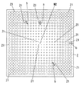
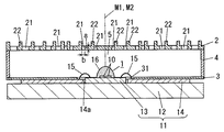
本実施形態のLED照明装置は、図1に示すように、発光波長の異なる複数のLEDチップ10を有する光源1と、光取り出し用の多数の開口部21が形成された矩形板状の拡散反射シートからなり光源1の光軸M1に厚み方向が一致する形で配置されるフェースシート2と、フェースシート2の光出射面側とは反対側においてフェースシート2に対向配置されフェースシート2で拡散反射された光をフェースシート2側へ拡散反射する矩形板状の拡散反射シートからなるリヤシート3と、フェースシート2とリヤリート3との間に介在する枠状(ここでは、矩形枠状)のスペーサ4とを備え、フェースシート2とリヤシート3との間の媒質5が空気であり、フェースシート2は、光源1からの直接光が外部へ出射せず且つ光出射面側の輝度が均一になるように各開口部21が形成されている。なお、スペーサ4の形状は枠状に限らず、例えば、柱状の形状として、フェースシート2とリヤシート3との四隅同士の間に介在させてもよい。
(Embodiment 1)
As shown in FIG. 1, the LED illumination device of the present embodiment is a rectangular plate-shaped diffuse reflection in which a
ここにおいて、光源1の各LEDチップ10は、1つの実装基板11の一表面側に実装され、透光性材料(例えば、シリコーン樹脂、エポキシ樹脂、アクリル樹脂、ポリカーボネート樹脂、ガラスなど)からなるレンズ状の封止部16により封止されている。実装基板11は、第1の熱伝導性材料(例えば、Cu、Alなど)からなる矩形板状の伝熱板12と、伝熱板12の一表面側の中央部に接合された第2の熱伝導性材料(例えば、AlNなど)からなる矩形板状のサブマウント部材13と、伝熱板12の上記一表面側に接合されサブマウント部材13が内側に離間して配置される開口窓14aを有する配線基板14とを備えており、配線基板14がリヤシート3に接合されている。ここで、サブマウント部材13は、LEDチップ10のチップサイズよりも大きなサイズの矩形板状に形成されLEDチップ10と伝熱板12との線膨張率差に起因してLEDチップ10に働く応力を緩和する応力緩和機能と、LEDチップ10で発生した熱を伝熱板12においてLEDチップ10のチップサイズよりも広い範囲に伝熱させる熱伝導機能とを有している。
Here, each
また、各LEDチップ10は、サブマウント部材13におけるLEDチップ10の搭載面側に形成された導体パターンと配線基板14の配線パターンとを電気的に接続する複数のボンディングワイヤ15を介して給電されるようになっている。ここで、配線基板14は、平面視において一部が伝熱板21の外周縁よりも外方へ延出する突出部(図示せず)が設けられており、当該突出部において電源ユニットなどからの給電用の電線が接続されるようになっている。なお、配線基板14としては、例えば、絶縁性基材の一表面側に各LEDチップ10への給電用の配線パターンが設けられたものを用いればよいが、絶縁性基材の材料としては、例えば、ガラスエポキシ樹脂(FR4、FR5など)、紙フェノールなどを採用すればよい。
Each
上述の光源1は、発光波長の異なる複数のLEDチップ10として、赤色光を放射する赤色LEDチップ、緑色光を放射する緑色LEDチップ、青色光を放射する青色LEDチップ、黄色光を放射する黄色LEDチップを採用しており、赤色光と緑色光と青色光と黄色光の混色光として白色光を得ることができる。ただし、LEDチップ10の数や発光色は特に限定するものではなく、所望の混色光に応じて適宜選択すればよい。
The
また、上述のスペーサ4は、フェースシート2およびリヤシート3と同様に、光源1からの光を反射する拡散反射シートにより構成されているが、スペーサ4は、必ずしも拡散反射シートにより構成する必要はない。
The
フェースシート2、リヤシート3およびスペーサ4に用いる拡散反射シートとしては、例えば、ポリエチレンテレフタレート樹脂(PET)を発泡させて10μm以下の超微細な気泡を多数形成した光反射板(超微細発泡光反射板)を用いればよく、この種の光反射板としては、例えば、MCPET(登録商標)を採用すればよいが、MCPETと同様に拡散反射率および全反射率の高いものであればMCPET以外のものを採用してもよく、シート状部材の表面に拡散反射膜を形成したものでもよい。本実施形態では、フェースシート2、リヤシート3およびスペーサ4を上述の拡散反射シートにより構成しているので、金属鏡面により反射面が形成されている場合に比べて、拡散反射率および全反射率を高めることができ、外部への光取り出し効率を高めることができ、光出力の向上を図れる。
As a diffuse reflection sheet used for the
リヤシート3は、サブマウント部材13が内側に離間して配置され且つ配線基板14における開口窓14aの周部を露出させる窓孔31が中央部に形成されている。
In the
また、フェースシート2は、上述のように、光源1からの直接光が外部へ出射せず且つ光出射面側の輝度が均一になるように各開口部21が形成されており、図1および図2に示すように、光源1に近い開口部21ほど開口サイズが小さく、光源1からの直接光が外部へ出射しないように光源1の光軸M1を含む断面(フェースシート2の厚み方向に沿った中心軸M2を含む断面)における各開口部21のアスペクト比が設定されている。ここにおいて、開口部21のアスペクト比は、フェースシート2における開口部21周部の厚みa(図1参照)とフェースシート2におけるリヤシート3側の表面における開口部21の幅b(図1参照)との比であり、〔アスペクト比〕=〔フェースシート2における開口部21周部の厚みa〕/〔開口部21の開口幅b〕により求められる値である。なお、本実施形態では、各開口部21の開口形状を円形状としてあり、フェースシート2の上記中心軸M2からの距離が大きな開口部21ほど開口幅bが大きくなっているが、開口部21の開口形状は円形状に限らず、例えば、図3に示すように、弧状の開口形状として、フェースシート2の上記中心軸M2からの距離が大きな開口部21ほど開口幅bが大きくなるようにしてもよい。
Further, as described above, each
以上説明した本実施形態のLED照明装置では、光取り出し用の多数の開口部21が形成された拡散反射シートからなり光源1の光軸M1に厚み方向が一致する形で配置されるフェースシート2と、フェースシート2の光出射面側とは反対側においてフェースシート2に対向配置されフェースシート2で拡散反射された光をフェースシート2側へ拡散反射する拡散反射シートからなるリヤシート3とを備え、フェースシート2とリヤシート3との間の媒質が空気なので、光取出し効率を向上でき、しかも、フェースシート2は、光源1からの直接光が外部へ出射せず且つ光出射面側の輝度が均一になるように各開口部21が形成されているので、発光波長の異なる複数のLEDチップ10を有する光源1において色むらがある場合でもLED照明装置全体として色むらの発生を抑制できる。また、本実施形態のLED照明装置では、フェースシート2とリヤシート3との間に枠状のスペーサ4を備え、スペーサ4も拡散反射シートにより形成されているので、外部への光取出し効率をさらに向上できる。
In the LED illumination device according to the present embodiment described above, the
また、本実施形態のLED照明装置によれば、フェースシート2は、光源1に近い開口部21ほど開口サイズが小さく、光源1からの直接光が外部へ出射しないように各開口部21のアスペクト比が設定されているので、光源1からの直接光が光源1に近い開口部21の内側面で反射されることなく出射するのを防止することができ、光源1からの直接光が開口部21を通して外部へ出射するのを防止することが可能となる。
Further, according to the LED lighting device of the present embodiment, the
また、本実施形態のLED照明装置では、光源1の点灯時に各LEDチップ10で発生した熱を配線基板14を通すことなくサブマウント部材13を介して伝熱板12へ伝熱して放熱することができるので、放熱性が向上し、各LEDチップ10のジャンクション温度の温度上昇を抑制できるから、入力電力を大きくでき、光出力の高出力化を図れる。
Further, in the LED lighting device of the present embodiment, the heat generated in each
(実施形態2)
本実施形態のLED照明装置の構成は実施形態1と略同じであって、図4に示すように、フェースシート2の構造が相違している。なお、実施形態1と同様の構成要素には同一の符号を付して説明を省略する。
(Embodiment 2)
The configuration of the LED lighting device of the present embodiment is substantially the same as that of the first embodiment, and the structure of the
本実施形態におけるフェースシート2は、光源1の光軸M1に近いほど厚みが厚く、光源1からの直接光が外部へ出射しないように各開口部21のアスペクト比が設定されている。なお、開口部21のアスペクト比の定義は基本的に実施形態1と同じであるが、開口部21のフェースシート2における開口部21周部の厚みaとしては、光源1の光軸M1を含む断面において光軸M1から遠い側の周部の厚みを採用する。
The
以上説明した本実施形態のLED照明装置では、開口部21の開口形状および開口サイズを実施形態1と同じに設定した場合に、光源1からの直接光が光源1に近い開口部21の内側面で反射されることなく出射するのをより確実に防止することができ、光源1からの直接光が開口部21を通して外部へ出射するのを防止することが可能となる。
In the LED lighting device of the present embodiment described above, when the opening shape and the opening size of the
(実施形態3)
本実施形態のLED照明装置の構成は実施形態1と略同じであって、図5に示すように、フェースシート2の構造が相違している。なお、実施形態1と同様の構成要素には同一の符号を付して説明を省略する。
(Embodiment 3)
The configuration of the LED lighting device of the present embodiment is substantially the same as that of the first embodiment, and the structure of the
ところで、実施形態2のLED照明装置では、フェースシート2において光源1の光軸M1に近い部位ほど厚みが厚くなっているので、輝度の均一性が低下してしまう。
By the way, in the LED illuminating device of
これに対して、本実施形態におけるフェースシート2は、光源1の光軸M1を含む断面における開口部21の内側面のうち光軸M1から遠い側が光軸M1に平行で光軸M1に近い側が光源1に近づくにつれて光軸M1から離れるテーパ状に形成されている。
On the other hand, in the
しかして、本実施形態のLED照明装置では、実施形態2に比べて、輝度の均一化を図れる。なお、実施形態2におけるフェースシート2の開口部21の形状を本実施形態と同様の形状としてもよい。
Therefore, in the LED lighting device of the present embodiment, it is possible to make the luminance uniform compared to the second embodiment. The shape of the
(実施形態4)
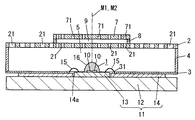
本実施形態のLED照明装置の構成は実施形態1と略同じであって、図6に示すように、フェースシート2の構造が相違している。なお、実施形態1と同様の構成要素には同一の符号を付して説明を省略する。
(Embodiment 4)
The configuration of the LED lighting device of the present embodiment is substantially the same as that of the first embodiment, and the structure of the
本実施形態におけるフェースシート2は、光出射面側における開口部21の周部のうち光源1の光軸M1から遠い側に厚み方向に突出し光源1からの直接光を反射する反射部22が形成されている。
The
しかして、本実施形態のLED照明装置では、光源1からの直接光の一部が1度も反射されずに開口部21を通過したとしても反射部22により反射されるので、光源1からの直接光が外部へ出射されるのをより確実に防止することが可能となる。
Thus, in the LED illumination device of the present embodiment, a part of the direct light from the
(実施形態5)
本実施形態のLED照明装置の構成は実施形態1と略同じであり、図7に示すように、フェースシート2の光出射面側に配置される矩形板状の導光板6であってフェースシート2の各開口部21それぞれに埋設される複数の導光部6bが連続一体に形成された導光板6を備えている点が相違する。なお、実施形態1と同様の構成要素には同一の符号を付して説明を省略する。
(Embodiment 5)
The configuration of the LED illumination device according to the present embodiment is substantially the same as that of the first embodiment, and as shown in FIG. 7, a rectangular plate-shaped
ここにおいて、導光板6の厚みは、当該導光板6での光損失をより少なくするために薄い方が好ましく、フェースシート2とリヤシート3との間の距離よりも小さく設定してある。また、導光板6は、ガラスにより形成してあるが、ガラスに限らず、例えば、アクリル樹脂、シリコーン樹脂、エポキシ樹脂、ポリカーボネート樹脂などにより形成してもよい。
Here, the thickness of the
しかして、本実施形態のLED照明装置では、フェースシート2の光出射面側に配置される導光板6を備えていることにより、フェースシート2の光出射面側へ出射した光が導光板6で導光されるので、輝度のより一層の均一化を図れる。
Therefore, in the LED illumination device of the present embodiment, the
また、本実施形態のLED照明装置では、導光板6におけるフェースシート2側とは反対側の表面に光取出し効率向上用の凹凸構造を形成すれば、外部への光取出し効率をさらに向上できる。なお、他の実施形態2〜4においても導光板6を設けてもよい。
Further, in the LED lighting device of the present embodiment, the light extraction efficiency to the outside can be further improved by forming a concavo-convex structure for improving the light extraction efficiency on the surface of the
(実施形態6)
本実施形態のLED照明装置の構成は実施形態1と略同じであって、図8に示すように、フェースシート2における光出射面側に離間して配置された拡散反射シートからなる2次フェースシート7を備え、2次フェースシート7は、光源1からの直接光が外部へ出射せず且つ当該2次フェースシート7の光出射面側の輝度が均一になるように多数の2次開口部71が形成されている点が相違する。なお、実施形態1と同様の構成要素には同一の符号を付して説明を省略する。
(Embodiment 6)
The configuration of the LED illumination device of the present embodiment is substantially the same as that of the first embodiment, and as shown in FIG. 8, a secondary face comprising a diffuse reflection sheet spaced apart on the light emitting surface side of the
2次フェースシート7は、フェースシート2と同様の拡散反射シートにより形成してあり、スペーサ8を介してフェースシート2に対向配置されている。したがって、2次フェースシート7とフェースシート2との間には、空隙9が形成されている。また、2次フェースシート7の開口部71は、フェースシート2の開口部21と同じ開口形状で開口部21の投影領域に形成してあるが、必ずしもフェースシート2の開口部21と同じ開口形状でなくてもよいし、形成位置もフェースシート2の開口部21の投影領域でなくてもよい。
The
以上説明した本実施形態のLED照明装置によれば、光源1からの直接光が外部へ出射されるのをより確実に防止することが可能となるとともに、輝度のより一層の均一化を図れる。なお、本実施形態では、2次フェースシート7の平面サイズをフェースシート2の平面サイズよりも小さく設定してあるが、フェースシート2と同じ平面サイズに設定してもよい。
According to the LED illumination device of the present embodiment described above, it is possible to more surely prevent direct light from the
1 光源
2 フェースシート
3 リヤシート
4 スペーサ
5 媒質
6 導光板
7 2次フェースシート
10 LEDチップ
21 開口部
22 反射部
31 窓孔
71 2次開口部
M1 光軸
M2 中心軸
DESCRIPTION OF
Claims (7)
Priority Applications (6)
| Application Number | Priority Date | Filing Date | Title |
|---|---|---|---|
| JP2008076699A JP5113573B2 (en) | 2008-03-24 | 2008-03-24 | LED lighting device |
| CN2009801103483A CN101978210B (en) | 2008-03-24 | 2009-03-24 | Led lighting device |
| KR1020107023715A KR101203133B1 (en) | 2008-03-24 | 2009-03-24 | Led lighting device |
| US12/933,486 US8742435B2 (en) | 2008-03-24 | 2009-03-24 | LED lighting device |
| EP09725294.4A EP2261551B1 (en) | 2008-03-24 | 2009-03-24 | Led lighting device |
| PCT/JP2009/055761 WO2009119550A1 (en) | 2008-03-24 | 2009-03-24 | Led illuminating apparatus |
Applications Claiming Priority (1)
| Application Number | Priority Date | Filing Date | Title |
|---|---|---|---|
| JP2008076699A JP5113573B2 (en) | 2008-03-24 | 2008-03-24 | LED lighting device |
Publications (2)
| Publication Number | Publication Date |
|---|---|
| JP2009231128A JP2009231128A (en) | 2009-10-08 |
| JP5113573B2 true JP5113573B2 (en) | 2013-01-09 |
Family
ID=41113742
Family Applications (1)
| Application Number | Title | Priority Date | Filing Date |
|---|---|---|---|
| JP2008076699A Active JP5113573B2 (en) | 2008-03-24 | 2008-03-24 | LED lighting device |
Country Status (6)
| Country | Link |
|---|---|
| US (1) | US8742435B2 (en) |
| EP (1) | EP2261551B1 (en) |
| JP (1) | JP5113573B2 (en) |
| KR (1) | KR101203133B1 (en) |
| CN (1) | CN101978210B (en) |
| WO (1) | WO2009119550A1 (en) |
Families Citing this family (63)
| Publication number | Priority date | Publication date | Assignee | Title |
|---|---|---|---|---|
| KR101702695B1 (en) * | 2009-11-16 | 2017-02-03 | 가부시키가이샤 오푸토 디자인 | Surface light source unit, surface illumination device, and liquid crystal display device |
| JP2011112423A (en) * | 2009-11-25 | 2011-06-09 | Hioki Ee Corp | Linear irradiator, and imaging unit for visual examination of substrate to be inspected containing linear irradiator |
| JP5457851B2 (en) * | 2010-01-19 | 2014-04-02 | パナソニック株式会社 | lighting equipment |
| JP2011150861A (en) * | 2010-01-20 | 2011-08-04 | Opt Design:Kk | Led light source device, and lighting system using the same |
| KR101707574B1 (en) * | 2010-03-16 | 2017-02-16 | 엘지전자 주식회사 | backlight unit having light blocking pattern and method for forming light blocking pattern of the same |
| US8355093B2 (en) * | 2010-03-16 | 2013-01-15 | Lg Electronics Inc. | Backlight unit and display device |
| WO2011132787A1 (en) * | 2010-04-23 | 2011-10-27 | 株式会社オプトデザイン | Surface illumination fixture and surface illumination device |
| JP2011249141A (en) * | 2010-05-26 | 2011-12-08 | Nittoh Kogaku Kk | Light emitting device |
| JP5433860B2 (en) * | 2010-06-25 | 2014-03-05 | 株式会社オプトデザイン | Lighting device |
| JP5584852B2 (en) * | 2010-07-16 | 2014-09-10 | 株式会社オプトデザイン | Surface illumination light source device |
| KR101191213B1 (en) | 2010-11-02 | 2012-10-15 | 엘지전자 주식회사 | Lighting apparatus |
| JP2012174634A (en) * | 2011-02-24 | 2012-09-10 | Sharp Corp | Light source module and optical member |
| CN102644883A (en) * | 2011-03-25 | 2012-08-22 | 京东方科技集团股份有限公司 | Direct type backlight source |
| JP5842274B2 (en) * | 2011-06-09 | 2016-01-13 | 株式会社オプトデザイン | Lighting device |
| KR20130051768A (en) * | 2011-11-10 | 2013-05-21 | 서울반도체 주식회사 | Surface illumination device |
| KR101910356B1 (en) * | 2012-04-04 | 2018-10-22 | 에스엘 주식회사 | Vehicle lamp with an inner component |
| DE102012209354A1 (en) * | 2012-04-30 | 2013-10-31 | At & S Austria Technologie & Systemtechnik Aktiengesellschaft | LED module |
| KR101961310B1 (en) * | 2012-07-09 | 2019-07-17 | 엘지이노텍 주식회사 | Light emitting device |
| US9632357B2 (en) * | 2012-07-17 | 2017-04-25 | Lg Electronics Inc. | Display device |
| EP2875278A4 (en) * | 2012-07-20 | 2015-09-23 | Sharp Kk | Lighting device and method for providing light |
| JP2014049275A (en) * | 2012-08-31 | 2014-03-17 | Toshiba Lighting & Technology Corp | Lighting apparatus |
| CN102997096A (en) * | 2012-11-19 | 2013-03-27 | 无锡莱吉特信息科技有限公司 | Lateral light inlet surface light source free of light guide plate |
| EP2959214B1 (en) * | 2013-02-19 | 2020-08-12 | Signify Holding B.V. | An arrangement comprising an optical device and a reflector |
| CN105026834B (en) * | 2013-02-25 | 2019-04-23 | 飞利浦照明控股有限公司 | lighting device |
| JP6292369B2 (en) * | 2013-04-18 | 2018-03-14 | 東芝ライテック株式会社 | Automotive interior lighting equipment |
| TWI510841B (en) * | 2013-07-23 | 2015-12-01 | Au Optronics Corp | Display device |
| DE112014004109B4 (en) | 2013-09-06 | 2021-05-20 | Sensor Electronic Technology Inc. | Diffuse ultraviolet lighting |
| JP2015088420A (en) * | 2013-11-01 | 2015-05-07 | 株式会社デンソー | Backlight unit |
| KR20150105169A (en) * | 2014-03-06 | 2015-09-16 | 교우세라 커넥터 프로덕츠 가부시키가이샤 | Lighting apparatus |
| JP6315179B2 (en) * | 2014-03-17 | 2018-04-25 | Tianma Japan株式会社 | Surface light emitting device and liquid crystal display device |
| KR102362100B1 (en) * | 2014-03-27 | 2022-02-11 | 도레이 카부시키가이샤 | Reflecting sheet, reflection unit for surface light source device, and surface light source device |
| KR102236711B1 (en) * | 2014-04-10 | 2021-04-06 | 엘지이노텍 주식회사 | Optical element and backlight unit including the same |
| US20160230955A1 (en) * | 2014-05-27 | 2016-08-11 | El Lighting Co., LTD. | Optical module |
| JP2015228315A (en) * | 2014-05-30 | 2015-12-17 | オムロン株式会社 | Diffused reflection structure and surface-emitting device comprising the same |
| JP6358896B2 (en) * | 2014-08-20 | 2018-07-18 | 三菱電機株式会社 | Surface light source device and liquid crystal display device |
| JP6358895B2 (en) | 2014-08-20 | 2018-07-18 | 三菱電機株式会社 | Surface light source device and liquid crystal display device |
| WO2016074898A1 (en) * | 2014-11-10 | 2016-05-19 | Philips Lighting Holding B.V. | Collimator for a lighting device, lighting device and method of manufacturing a collimator |
| JPWO2016104023A1 (en) * | 2014-12-25 | 2017-10-05 | 株式会社Nano Wave | Light emitting device |
| KR102362197B1 (en) | 2015-02-02 | 2022-02-11 | 삼성디스플레이 주식회사 | Backlight assembly and liquid crystal display device comprising the same |
| KR101723291B1 (en) * | 2015-04-29 | 2017-04-04 | 주식회사 다비스 | Lighting apparatus using light emitting diode |
| CN106940005A (en) * | 2015-05-07 | 2017-07-11 | 赵志强 | A kind of LED wall bricks |
| TWI541472B (en) * | 2015-06-11 | 2016-07-11 | 友達光電股份有限公司 | Backlight module |
| JP6373231B2 (en) * | 2015-06-30 | 2018-08-15 | 古河電気工業株式会社 | Illumination device and light extraction method from illumination device |
| JP6200458B2 (en) * | 2015-06-30 | 2017-09-20 | 古河電気工業株式会社 | LED lighting device |
| EP3426974B1 (en) * | 2016-03-11 | 2021-02-17 | Signify Holding B.V. | Lighting device with sparkling effect |
| CN108886072A (en) * | 2016-04-05 | 2018-11-23 | 飞利浦照明控股有限公司 | Optical switching equipment with the wavelength conversion layer with hydrophobic nano structure |
| JP2019511828A (en) * | 2016-04-22 | 2019-04-25 | シグニファイ ホールディング ビー ヴィ | Integrated air guide and beam shaping |
| JP6636651B2 (en) * | 2016-04-22 | 2020-01-29 | シグニファイ ホールディング ビー ヴィSignify Holding B.V. | Pebble louver |
| WO2017182370A1 (en) * | 2016-04-22 | 2017-10-26 | Philips Lighting Holding B.V. | Integrated air guide and beam shaping' |
| CN109844401A (en) * | 2016-10-26 | 2019-06-04 | 夏普株式会社 | Lighting device and display device |
| US10274783B2 (en) * | 2017-05-05 | 2019-04-30 | Pelka & Associates, Inc. | Direct-view LED backlight with gradient reflective layer |
| CN110612417A (en) * | 2017-05-17 | 2019-12-24 | 夏普株式会社 | Backlight unit, display device, manufacturing method of backlight unit, and manufacturing device of backlight unit |
| WO2019013216A1 (en) | 2017-07-11 | 2019-01-17 | 古河電気工業株式会社 | Led illumination device with speaker function, and method for extracting light and sound from led illumination device with speaker function |
| WO2019134829A1 (en) * | 2018-01-02 | 2019-07-11 | Signify Holding B.V. | Lighting module, kit and panel |
| TWI686651B (en) * | 2018-11-23 | 2020-03-01 | 友達光電股份有限公司 | Backlight module |
| KR102218345B1 (en) * | 2019-01-23 | 2021-02-22 | 주식회사 지엘비젼 | Lighting devicee |
| CN110441957B (en) * | 2019-06-10 | 2021-06-11 | 惠科股份有限公司 | Display module assembly and display device |
| KR20220019975A (en) * | 2020-08-11 | 2022-02-18 | 엘지이노텍 주식회사 | Lighting apparatus and lamp including the same |
| CN112684636A (en) * | 2021-01-20 | 2021-04-20 | 惠科股份有限公司 | Backlight module and display device |
| US11835213B2 (en) | 2021-08-19 | 2023-12-05 | Matthew Hartley | Lighting fixtures with improved lighting components |
| CN116243519B (en) | 2021-12-08 | 2025-01-14 | 日亚化学工业株式会社 | Light-emitting module and planar light source |
| JP7458581B2 (en) * | 2021-12-08 | 2024-04-01 | 日亜化学工業株式会社 | Light emitting module and surface light source |
| EP4696607A1 (en) * | 2024-08-14 | 2026-02-18 | Goodrich Lighting Systems GmbH & Co. KG | Aircraft tail navigation light, aircraft comprising an aircraft tail navigation light, and method of operating an aircraft tail navigation light |
Family Cites Families (17)
| Publication number | Priority date | Publication date | Assignee | Title |
|---|---|---|---|---|
| US4146883A (en) * | 1977-09-12 | 1979-03-27 | Minnesota Mining And Manufacturing Company | Display |
| JPH08153405A (en) * | 1994-06-21 | 1996-06-11 | Nakaya:Kk | Surface light source |
| JPH10106327A (en) * | 1996-10-02 | 1998-04-24 | Kuraray Co Ltd | Surface light source element and display apparatus using the element |
| US6878969B2 (en) * | 2002-07-29 | 2005-04-12 | Matsushita Electric Works, Ltd. | Light emitting device |
| US7211831B2 (en) * | 2003-04-15 | 2007-05-01 | Luminus Devices, Inc. | Light emitting device with patterned surfaces |
| US6995355B2 (en) * | 2003-06-23 | 2006-02-07 | Advanced Optical Technologies, Llc | Optical integrating chamber lighting using multiple color sources |
| US6921929B2 (en) * | 2003-06-27 | 2005-07-26 | Lockheed Martin Corporation | Light-emitting diode (LED) with amorphous fluoropolymer encapsulant and lens |
| US7997771B2 (en) * | 2004-06-01 | 2011-08-16 | 3M Innovative Properties Company | LED array systems |
| JP3821141B2 (en) * | 2004-06-14 | 2006-09-13 | ソニー株式会社 | Backlight device and liquid crystal display device |
| JP4691917B2 (en) | 2004-07-12 | 2011-06-01 | ソニー株式会社 | Display equipment |
| JP2006027886A (en) * | 2004-07-21 | 2006-02-02 | Hitachi Building Systems Co Ltd | Elevator sharing prevention method |
| US7323721B2 (en) * | 2004-09-09 | 2008-01-29 | Blue Photonics Inc. | Monolithic multi-color, multi-quantum well semiconductor LED |
| JP2007012323A (en) * | 2005-06-28 | 2007-01-18 | Cheil Ind Co Ltd | Surface light source device, and liquid crystal display device |
| WO2007072919A1 (en) * | 2005-12-22 | 2007-06-28 | Matsushita Electric Works, Ltd. | Illumination instrument using led |
| KR101220204B1 (en) * | 2005-12-28 | 2013-01-09 | 엘지디스플레이 주식회사 | Light Emitting Diodes back-light assembly and liquid crystal display device module using thereof |
| JP4280283B2 (en) * | 2006-01-27 | 2009-06-17 | 株式会社オプトデザイン | Surface illumination light source device and surface illumination device using the same |
| JP2008027866A (en) | 2006-07-25 | 2008-02-07 | Toyota Motor Corp | Fuel cell |
-
2008
- 2008-03-24 JP JP2008076699A patent/JP5113573B2/en active Active
-
2009
- 2009-03-24 US US12/933,486 patent/US8742435B2/en active Active
- 2009-03-24 WO PCT/JP2009/055761 patent/WO2009119550A1/en not_active Ceased
- 2009-03-24 EP EP09725294.4A patent/EP2261551B1/en active Active
- 2009-03-24 CN CN2009801103483A patent/CN101978210B/en active Active
- 2009-03-24 KR KR1020107023715A patent/KR101203133B1/en not_active Expired - Fee Related
Also Published As
| Publication number | Publication date |
|---|---|
| WO2009119550A1 (en) | 2009-10-01 |
| KR20100124839A (en) | 2010-11-29 |
| EP2261551A4 (en) | 2014-07-16 |
| EP2261551A1 (en) | 2010-12-15 |
| JP2009231128A (en) | 2009-10-08 |
| KR101203133B1 (en) | 2012-11-20 |
| EP2261551B1 (en) | 2019-05-08 |
| CN101978210A (en) | 2011-02-16 |
| US8742435B2 (en) | 2014-06-03 |
| US20110018012A1 (en) | 2011-01-27 |
| CN101978210B (en) | 2013-04-03 |
Similar Documents
| Publication | Publication Date | Title |
|---|---|---|
| JP5113573B2 (en) | LED lighting device | |
| CN103486511B (en) | Lamp unit and the vehicle using the lamp unit | |
| JP5025612B2 (en) | LED light source and light emitter using the same | |
| JP5066462B2 (en) | Vehicle lighting | |
| US8585237B2 (en) | Lighting module | |
| CN101319759B (en) | Light emitting device, area light source apparatus and image display apparatus | |
| CN101627326B (en) | Device with semiconductor chip and light guiding layer | |
| CN111025743B (en) | Light source module and display device | |
| JP2006286639A (en) | Light emitting device having a plurality of overlapping panels forming recesses for emitting light | |
| US20110180832A1 (en) | Light emitting device package | |
| JP2006286638A (en) | Light emitting device having a plurality of adjacently overlapping light guide plates | |
| CN101275720A (en) | LED lighting device | |
| CN111458925A (en) | Light source module and display device | |
| JP2015103323A (en) | Lighting device | |
| JP5738309B2 (en) | Light emitting module | |
| JP5538479B2 (en) | LED light source and light emitter using the same | |
| KR20130081868A (en) | Lens unit and light-emitting apparatus | |
| CN111722434A (en) | Light source module and display device | |
| KR101039738B1 (en) | Light guide plate cartridge, backlight unit and display device including same | |
| CN215867197U (en) | Light guide plate and light guide plate system | |
| JP2012227537A (en) | Led light source and luminous body using the same | |
| KR20130095051A (en) | Ligout source package and backlight unit including the same | |
| TWI313336B (en) | Light emitting diode lamp | |
| WO2024053572A1 (en) | Optical member and illumination device | |
| JP2024508662A (en) | Light emitting element package and lighting device equipped with the same |
Legal Events
| Date | Code | Title | Description |
|---|---|---|---|
| RD04 | Notification of resignation of power of attorney |
Free format text: JAPANESE INTERMEDIATE CODE: A7424 Effective date: 20100811 |
|
| A621 | Written request for application examination |
Free format text: JAPANESE INTERMEDIATE CODE: A621 Effective date: 20101022 |
|
| A711 | Notification of change in applicant |
Free format text: JAPANESE INTERMEDIATE CODE: A712 Effective date: 20120112 |
|
| A131 | Notification of reasons for refusal |
Free format text: JAPANESE INTERMEDIATE CODE: A131 Effective date: 20120522 |
|
| A521 | Request for written amendment filed |
Free format text: JAPANESE INTERMEDIATE CODE: A523 Effective date: 20120723 |
|
| TRDD | Decision of grant or rejection written | ||
| A01 | Written decision to grant a patent or to grant a registration (utility model) |
Free format text: JAPANESE INTERMEDIATE CODE: A01 Effective date: 20120918 |
|
| A01 | Written decision to grant a patent or to grant a registration (utility model) |
Free format text: JAPANESE INTERMEDIATE CODE: A01 |
|
| A61 | First payment of annual fees (during grant procedure) |
Free format text: JAPANESE INTERMEDIATE CODE: A61 Effective date: 20121012 |
|
| FPAY | Renewal fee payment (event date is renewal date of database) |
Free format text: PAYMENT UNTIL: 20151019 Year of fee payment: 3 |
|
| R150 | Certificate of patent or registration of utility model |
Ref document number: 5113573 Country of ref document: JP Free format text: JAPANESE INTERMEDIATE CODE: R150 Free format text: JAPANESE INTERMEDIATE CODE: R150 |