JP5057980B2 - プラズマ加工システムで基板の属性を現場でモニターするためのモニター方法 - Google Patents
プラズマ加工システムで基板の属性を現場でモニターするためのモニター方法 Download PDFInfo
- Publication number
- JP5057980B2 JP5057980B2 JP2007533669A JP2007533669A JP5057980B2 JP 5057980 B2 JP5057980 B2 JP 5057980B2 JP 2007533669 A JP2007533669 A JP 2007533669A JP 2007533669 A JP2007533669 A JP 2007533669A JP 5057980 B2 JP5057980 B2 JP 5057980B2
- Authority
- JP
- Japan
- Prior art keywords
- plasma
- substrate
- plasma processing
- frequency
- attribute
- Prior art date
- Legal status (The legal status is an assumption and is not a legal conclusion. Google has not performed a legal analysis and makes no representation as to the accuracy of the status listed.)
- Active
Links
- 238000012545 processing Methods 0.000 title claims description 77
- 239000000758 substrate Substances 0.000 title claims description 62
- 238000000034 method Methods 0.000 title claims description 34
- 238000012544 monitoring process Methods 0.000 title claims description 12
- 238000005530 etching Methods 0.000 claims description 17
- 239000000523 sample Substances 0.000 claims description 13
- 230000008569 process Effects 0.000 claims description 12
- 239000007789 gas Substances 0.000 description 15
- 238000010586 diagram Methods 0.000 description 12
- 238000005259 measurement Methods 0.000 description 11
- 230000000875 corresponding effect Effects 0.000 description 8
- 230000002596 correlated effect Effects 0.000 description 7
- 238000004519 manufacturing process Methods 0.000 description 7
- 238000011109 contamination Methods 0.000 description 5
- 238000011156 evaluation Methods 0.000 description 5
- 229920002120 photoresistant polymer Polymers 0.000 description 5
- 230000015556 catabolic process Effects 0.000 description 4
- 238000006731 degradation reaction Methods 0.000 description 4
- 239000000463 material Substances 0.000 description 4
- 238000004140 cleaning Methods 0.000 description 3
- 238000001816 cooling Methods 0.000 description 3
- 230000008878 coupling Effects 0.000 description 3
- 238000010168 coupling process Methods 0.000 description 3
- 238000005859 coupling reaction Methods 0.000 description 3
- 239000001307 helium Substances 0.000 description 3
- 229910052734 helium Inorganic materials 0.000 description 3
- SWQJXJOGLNCZEY-UHFFFAOYSA-N helium atom Chemical compound [He] SWQJXJOGLNCZEY-UHFFFAOYSA-N 0.000 description 3
- 150000002500 ions Chemical class 0.000 description 3
- RYGMFSIKBFXOCR-UHFFFAOYSA-N Copper Chemical compound [Cu] RYGMFSIKBFXOCR-UHFFFAOYSA-N 0.000 description 2
- 230000009471 action Effects 0.000 description 2
- 230000008901 benefit Effects 0.000 description 2
- 230000008859 change Effects 0.000 description 2
- 239000004020 conductor Substances 0.000 description 2
- 229910052802 copper Inorganic materials 0.000 description 2
- 239000010949 copper Substances 0.000 description 2
- 238000009826 distribution Methods 0.000 description 2
- 230000009977 dual effect Effects 0.000 description 2
- 239000000839 emulsion Substances 0.000 description 2
- 239000011521 glass Substances 0.000 description 2
- 238000010849 ion bombardment Methods 0.000 description 2
- 238000011160 research Methods 0.000 description 2
- 239000004065 semiconductor Substances 0.000 description 2
- 238000012360 testing method Methods 0.000 description 2
- 229910052581 Si3N4 Inorganic materials 0.000 description 1
- ATJFFYVFTNAWJD-UHFFFAOYSA-N Tin Chemical compound [Sn] ATJFFYVFTNAWJD-UHFFFAOYSA-N 0.000 description 1
- XAGFODPZIPBFFR-UHFFFAOYSA-N aluminium Chemical compound [Al] XAGFODPZIPBFFR-UHFFFAOYSA-N 0.000 description 1
- 229910052782 aluminium Inorganic materials 0.000 description 1
- 238000004458 analytical method Methods 0.000 description 1
- 230000004888 barrier function Effects 0.000 description 1
- 239000000356 contaminant Substances 0.000 description 1
- 230000001276 controlling effect Effects 0.000 description 1
- 239000002826 coolant Substances 0.000 description 1
- 238000000151 deposition Methods 0.000 description 1
- 238000002405 diagnostic procedure Methods 0.000 description 1
- 230000005684 electric field Effects 0.000 description 1
- 238000005516 engineering process Methods 0.000 description 1
- 230000006870 function Effects 0.000 description 1
- 238000007429 general method Methods 0.000 description 1
- 230000017525 heat dissipation Effects 0.000 description 1
- 230000006872 improvement Effects 0.000 description 1
- 238000011065 in-situ storage Methods 0.000 description 1
- 230000001939 inductive effect Effects 0.000 description 1
- 238000012423 maintenance Methods 0.000 description 1
- 239000000203 mixture Substances 0.000 description 1
- 238000012986 modification Methods 0.000 description 1
- 230000004048 modification Effects 0.000 description 1
- NJPPVKZQTLUDBO-UHFFFAOYSA-N novaluron Chemical compound C1=C(Cl)C(OC(F)(F)C(OC(F)(F)F)F)=CC=C1NC(=O)NC(=O)C1=C(F)C=CC=C1F NJPPVKZQTLUDBO-UHFFFAOYSA-N 0.000 description 1
- 238000005498 polishing Methods 0.000 description 1
- 230000003449 preventive effect Effects 0.000 description 1
- 238000003672 processing method Methods 0.000 description 1
- 230000009467 reduction Effects 0.000 description 1
- 238000002310 reflectometry Methods 0.000 description 1
- HQVNEWCFYHHQES-UHFFFAOYSA-N silicon nitride Chemical compound N12[Si]34N5[Si]62N3[Si]51N64 HQVNEWCFYHHQES-UHFFFAOYSA-N 0.000 description 1
- 239000000126 substance Substances 0.000 description 1
- 230000026676 system process Effects 0.000 description 1
- 239000010409 thin film Substances 0.000 description 1
- 238000012546 transfer Methods 0.000 description 1
Images


Classifications
-
- H—ELECTRICITY
- H01—ELECTRIC ELEMENTS
- H01J—ELECTRIC DISCHARGE TUBES OR DISCHARGE LAMPS
- H01J37/00—Discharge tubes with provision for introducing objects or material to be exposed to the discharge, e.g. for the purpose of examination or processing thereof
- H01J37/32—Gas-filled discharge tubes
- H01J37/32917—Plasma diagnostics
- H01J37/32935—Monitoring and controlling tubes by information coming from the object and/or discharge
-
- H—ELECTRICITY
- H01—ELECTRIC ELEMENTS
- H01L—SEMICONDUCTOR DEVICES NOT COVERED BY CLASS H10
- H01L21/00—Processes or apparatus adapted for the manufacture or treatment of semiconductor or solid state devices or of parts thereof
- H01L21/02—Manufacture or treatment of semiconductor devices or of parts thereof
- H01L21/04—Manufacture or treatment of semiconductor devices or of parts thereof the devices having potential barriers, e.g. a PN junction, depletion layer or carrier concentration layer
- H01L21/18—Manufacture or treatment of semiconductor devices or of parts thereof the devices having potential barriers, e.g. a PN junction, depletion layer or carrier concentration layer the devices having semiconductor bodies comprising elements of Group IV of the Periodic Table or AIIIBV compounds with or without impurities, e.g. doping materials
- H01L21/30—Treatment of semiconductor bodies using processes or apparatus not provided for in groups H01L21/20 - H01L21/26
- H01L21/302—Treatment of semiconductor bodies using processes or apparatus not provided for in groups H01L21/20 - H01L21/26 to change their surface-physical characteristics or shape, e.g. etching, polishing, cutting
- H01L21/306—Chemical or electrical treatment, e.g. electrolytic etching
Landscapes
- Engineering & Computer Science (AREA)
- Physics & Mathematics (AREA)
- Microelectronics & Electronic Packaging (AREA)
- General Physics & Mathematics (AREA)
- Manufacturing & Machinery (AREA)
- Computer Hardware Design (AREA)
- Condensed Matter Physics & Semiconductors (AREA)
- Power Engineering (AREA)
- Plasma & Fusion (AREA)
- Chemical & Material Sciences (AREA)
- Analytical Chemistry (AREA)
- Drying Of Semiconductors (AREA)
- Plasma Technology (AREA)
Description
Xは特定評価値であり、μは平均値であり、Nは評価値数である。
供給電力は一般的に次の様に計算できる。
インピーダンス、複素数、は一般的に次の様に計算できる。
V0が基部での電圧(ピーク電圧)である場合、I0は基部での電流(ピーク電流)であり、Rは実抵抗であり、j=sqrt(−1)(複素数の虚数部)であり、Xはコンプレックスリアクタンスである。コンプレックスリアクタンスは、電流及び電圧がωで表わされる角周波数を有した発生信号のそれぞれのACサイクルと共に変動するとき、電子部品がエネルギーを保存及び放出する程度のことである。
プラズマインピーダンスの位相角は次の式で表わすことができる。
R=Zcos(θ)でX=Zsin(θ)である。
電力(2MHz):1000.0ワット
電力(27MHz):2000.0ワット
混合ガス:5 SCCM CH2F2,6 SCCM C4F8,180 SCCM N2及び200 SCCM AR
温度: TP(上部)で80℃及びESCで20℃
加工時間: 60秒間
CW:37
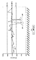
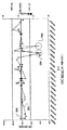
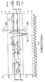
プロット202は数週間に渡ったブランケット酸化物のエッチング速度をナノメータ毎分(nm/分)で表している。この図を分析すると2つのエクスカーションポイントが明らかとなる:2004年4月6日実施の204と2004年4月9日実施の206である。前述のごとくエクスカーションは設定統計範囲または値範囲を外れているデータポイントを表し、数々の要素(すなわち、チャンバ汚染、プラズマ構造ダメージ及び劣化、ガス圧漏出、ガス流混合問題、仕様を外れたチャンバ温度、劣悪RFケーブル、不適当に接続されたケーブル、裏側Heフロー等々)によって発生する。
2004年4月6日に示すように、エッチングプロット202とプロットHeフロー208は共に204でエクスカーションを示している。すなわち、Heフローは約33.5SCCMへ減少し、エッチング速度も実質的に約33.4nm/分へ減少し、実質的に100.91nm/分である3σ制御下限を外れている。
Claims (9)
- プラズマ加工チャンバを有したプラズマ加工システムで基板の属性を現場でモニターするためのモニター方法であって、
前記プラズマ加工チャンバ内に基板を配置するステップと、
前記基板が前記プラズマ加工チャンバ内に配置されているときに該プラズマ加工チャンバ内でプラズマを放射するステップと、
一連のプラズマパラメータの値を測定するステップであって、前記プラズマパラメータが、特定周波数のRF電源のインピーダンス、周波数調整されたプラズマシステムのRF周波数、特定周波数のRF電源の位相角、の中のいずれかであるステップと、を備えており、
一連の前記プラズマパラメータの値が設定されている統計的範囲を外れていれば、前記基板の前記属性のエクスカーションの特定の種類が発生したと推定し、一連の前記プラズマパラメータの値が設定されている統計的範囲を外れている場合に前記基板の前記属性のエクスカーションの特定の種類の推定に役立つデータを発生させるために、前記基板の前記属性は、基板の工程の履歴データを用いて前記プラズマパラメータと予め関連づけられていることを特徴としており、
且つ前記基板の前記属性が、エッチング速度、選択度、エッチング均一性の測定値の中のいずれか一つであることを特徴とする方法。 - プラズマ加工システムはV/Iプローブを含んでおり、前記一連のプラズマパラメータの値は前記V/Iプローブを利用して測定されることを特徴とする請求項1記載の方法。
- 測定された前記一連のプラズマパラメータの値は、前記特定周波数の前記RF電源の位相角であることを特徴とする請求項1記載の方法。
- 測定された前記一連のプラズマパラメータの値は、前記特定周波数の前記RF電源のインピーダンスであることを特徴とする請求項1記載の方法。
- 測定された前記一連のプラズマパラメータの値は、前記周波数調整されたプラズマシステムのRF周波数であることを特徴とする請求項1記載の方法。
- 前記基板属性は、基板エッチング中の前記エッチング速度であることを特徴とする請求項1記載の方法。
- 前記基板属性は、基板エッチング中の前記選択度であることを特徴とする請求項1記載の方法。
- 前記基板属性は、基板エッチング中の前記エッチング均一性の測定値であることを特徴とする請求項1記載の方法。
- 前記プラズマ加工システムは、周波数調整結合プラズマ加工システムであることを特徴とする請求項1記載の方法。
Applications Claiming Priority (3)
| Application Number | Priority Date | Filing Date | Title |
|---|---|---|---|
| US10/951,553 | 2004-09-27 | ||
| US10/951,553 US7323116B2 (en) | 2004-09-27 | 2004-09-27 | Methods and apparatus for monitoring a process in a plasma processing system by measuring self-bias voltage |
| PCT/US2005/034227 WO2006036821A2 (en) | 2004-09-27 | 2005-09-23 | Methods and apparatus for monitoring a process in a plasma processing system by measuring self-bias voltage |
Publications (3)
| Publication Number | Publication Date |
|---|---|
| JP2008515198A JP2008515198A (ja) | 2008-05-08 |
| JP2008515198A5 JP2008515198A5 (ja) | 2008-11-13 |
| JP5057980B2 true JP5057980B2 (ja) | 2012-10-24 |
Family
ID=36097829
Family Applications (1)
| Application Number | Title | Priority Date | Filing Date |
|---|---|---|---|
| JP2007533669A Active JP5057980B2 (ja) | 2004-09-27 | 2005-09-23 | プラズマ加工システムで基板の属性を現場でモニターするためのモニター方法 |
Country Status (6)
| Country | Link |
|---|---|
| US (1) | US7323116B2 (ja) |
| JP (1) | JP5057980B2 (ja) |
| KR (1) | KR101164828B1 (ja) |
| CN (1) | CN101088147B (ja) |
| TW (1) | TWI398626B (ja) |
| WO (1) | WO2006036821A2 (ja) |
Families Citing this family (55)
| Publication number | Priority date | Publication date | Assignee | Title |
|---|---|---|---|---|
| JP4416569B2 (ja) * | 2004-05-24 | 2010-02-17 | キヤノン株式会社 | 堆積膜形成方法および堆積膜形成装置 |
| JP4657949B2 (ja) * | 2006-03-01 | 2011-03-23 | 株式会社日立ハイテクノロジーズ | エッチング処理装置および自己バイアス電圧測定方法ならびにエッチング処理装置の監視方法 |
| DE102007000611A1 (de) * | 2007-10-31 | 2009-05-07 | Fraunhofer-Gesellschaft zur Förderung der angewandten Forschung e.V. | Kratzfeste und dehnbare Korrosionsschutzschicht für Leichtmetallsubstrate |
| CN101470455B (zh) * | 2007-12-29 | 2011-06-15 | 北京北方微电子基地设备工艺研究中心有限责任公司 | 一种补偿直流自偏压的方法及系统、半导体处理设备 |
| TWI475592B (zh) * | 2008-07-07 | 2015-03-01 | Lam Res Corp | 用來偵測電漿處理腔室中之電漿不穩定性的被動電容耦合靜電探針裝置 |
| JP2010199475A (ja) * | 2009-02-27 | 2010-09-09 | Tokyo Electron Ltd | プラズマ処理装置のクリーニング方法及び記憶媒体 |
| DE102009016701A1 (de) * | 2009-04-06 | 2010-10-14 | Forschungsverbund Berlin E.V. | Prozesskammer mit modulierter Plasmaversorgung |
| US8501631B2 (en) | 2009-11-19 | 2013-08-06 | Lam Research Corporation | Plasma processing system control based on RF voltage |
| US9111729B2 (en) * | 2009-12-03 | 2015-08-18 | Lam Research Corporation | Small plasma chamber systems and methods |
| US9190289B2 (en) | 2010-02-26 | 2015-11-17 | Lam Research Corporation | System, method and apparatus for plasma etch having independent control of ion generation and dissociation of process gas |
| US9117767B2 (en) | 2011-07-21 | 2015-08-25 | Lam Research Corporation | Negative ion control for dielectric etch |
| US9967965B2 (en) | 2010-08-06 | 2018-05-08 | Lam Research Corporation | Distributed, concentric multi-zone plasma source systems, methods and apparatus |
| US9449793B2 (en) | 2010-08-06 | 2016-09-20 | Lam Research Corporation | Systems, methods and apparatus for choked flow element extraction |
| US9155181B2 (en) | 2010-08-06 | 2015-10-06 | Lam Research Corporation | Distributed multi-zone plasma source systems, methods and apparatus |
| US8999104B2 (en) | 2010-08-06 | 2015-04-07 | Lam Research Corporation | Systems, methods and apparatus for separate plasma source control |
| US9177762B2 (en) | 2011-11-16 | 2015-11-03 | Lam Research Corporation | System, method and apparatus of a wedge-shaped parallel plate plasma reactor for substrate processing |
| US10283325B2 (en) | 2012-10-10 | 2019-05-07 | Lam Research Corporation | Distributed multi-zone plasma source systems, methods and apparatus |
| US8872525B2 (en) | 2011-11-21 | 2014-10-28 | Lam Research Corporation | System, method and apparatus for detecting DC bias in a plasma processing chamber |
| US9083182B2 (en) | 2011-11-21 | 2015-07-14 | Lam Research Corporation | Bypass capacitors for high voltage bias power in the mid frequency RF range |
| US9396908B2 (en) | 2011-11-22 | 2016-07-19 | Lam Research Corporation | Systems and methods for controlling a plasma edge region |
| US8898889B2 (en) | 2011-11-22 | 2014-12-02 | Lam Research Corporation | Chuck assembly for plasma processing |
| US9263240B2 (en) * | 2011-11-22 | 2016-02-16 | Lam Research Corporation | Dual zone temperature control of upper electrodes |
| US10586686B2 (en) | 2011-11-22 | 2020-03-10 | Law Research Corporation | Peripheral RF feed and symmetric RF return for symmetric RF delivery |
| WO2013078098A1 (en) * | 2011-11-23 | 2013-05-30 | Lam Research Corporation | Multi zone gas injection upper electrode system |
| KR102011535B1 (ko) | 2011-11-24 | 2019-08-16 | 램 리써치 코포레이션 | 가요성 있는 대칭적 rf 복귀 스트랩을 갖는 플라즈마 프로세싱 챔버 |
| US10157729B2 (en) | 2012-02-22 | 2018-12-18 | Lam Research Corporation | Soft pulsing |
| US9368329B2 (en) | 2012-02-22 | 2016-06-14 | Lam Research Corporation | Methods and apparatus for synchronizing RF pulses in a plasma processing system |
| US9462672B2 (en) | 2012-02-22 | 2016-10-04 | Lam Research Corporation | Adjustment of power and frequency based on three or more states |
| US9390893B2 (en) | 2012-02-22 | 2016-07-12 | Lam Research Corporation | Sub-pulsing during a state |
| US9295148B2 (en) | 2012-12-14 | 2016-03-22 | Lam Research Corporation | Computation of statistics for statistical data decimation |
| US9502216B2 (en) | 2013-01-31 | 2016-11-22 | Lam Research Corporation | Using modeling to determine wafer bias associated with a plasma system |
| US9171699B2 (en) | 2012-02-22 | 2015-10-27 | Lam Research Corporation | Impedance-based adjustment of power and frequency |
| US9530620B2 (en) | 2013-03-15 | 2016-12-27 | Lam Research Corporation | Dual control modes |
| US9842725B2 (en) | 2013-01-31 | 2017-12-12 | Lam Research Corporation | Using modeling to determine ion energy associated with a plasma system |
| US9197196B2 (en) | 2012-02-22 | 2015-11-24 | Lam Research Corporation | State-based adjustment of power and frequency |
| US9320126B2 (en) | 2012-12-17 | 2016-04-19 | Lam Research Corporation | Determining a value of a variable on an RF transmission model |
| US10325759B2 (en) | 2012-02-22 | 2019-06-18 | Lam Research Corporation | Multiple control modes |
| US9114666B2 (en) | 2012-02-22 | 2015-08-25 | Lam Research Corporation | Methods and apparatus for controlling plasma in a plasma processing system |
| US10128090B2 (en) | 2012-02-22 | 2018-11-13 | Lam Research Corporation | RF impedance model based fault detection |
| US9408288B2 (en) | 2012-09-14 | 2016-08-02 | Lam Research Corporation | Edge ramping |
| US9043525B2 (en) | 2012-12-14 | 2015-05-26 | Lam Research Corporation | Optimizing a rate of transfer of data between an RF generator and a host system within a plasma tool |
| US9155182B2 (en) | 2013-01-11 | 2015-10-06 | Lam Research Corporation | Tuning a parameter associated with plasma impedance |
| US9779196B2 (en) | 2013-01-31 | 2017-10-03 | Lam Research Corporation | Segmenting a model within a plasma system |
| US9620337B2 (en) | 2013-01-31 | 2017-04-11 | Lam Research Corporation | Determining a malfunctioning device in a plasma system |
| US9107284B2 (en) | 2013-03-13 | 2015-08-11 | Lam Research Corporation | Chamber matching using voltage control mode |
| US9119283B2 (en) | 2013-03-14 | 2015-08-25 | Lam Research Corporation | Chamber matching for power control mode |
| US9502221B2 (en) | 2013-07-26 | 2016-11-22 | Lam Research Corporation | Etch rate modeling and use thereof with multiple parameters for in-chamber and chamber-to-chamber matching |
| US9594105B2 (en) | 2014-01-10 | 2017-03-14 | Lam Research Corporation | Cable power loss determination for virtual metrology |
| US10950421B2 (en) | 2014-04-21 | 2021-03-16 | Lam Research Corporation | Using modeling for identifying a location of a fault in an RF transmission system for a plasma system |
| US9536749B2 (en) | 2014-12-15 | 2017-01-03 | Lam Research Corporation | Ion energy control by RF pulse shape |
| JP2018041217A (ja) | 2016-09-06 | 2018-03-15 | 東京エレクトロン株式会社 | 異常検知方法及び半導体製造装置 |
| US10536130B2 (en) | 2017-08-29 | 2020-01-14 | Mks Instruments, Inc. | Balancing RF circuit and control for a cross-coupled SIMO distribution network |
| JP7258562B2 (ja) * | 2019-01-11 | 2023-04-17 | 東京エレクトロン株式会社 | 処理方法及びプラズマ処理装置 |
| CN113035677B (zh) * | 2019-12-09 | 2023-01-24 | 中微半导体设备(上海)股份有限公司 | 等离子体处理设备以及等离子体处理方法 |
| CN112888128B (zh) * | 2021-01-18 | 2023-04-07 | 南昌大学 | 一种测量等离子体离子非广延参数的方法 |
Family Cites Families (19)
| Publication number | Priority date | Publication date | Assignee | Title |
|---|---|---|---|---|
| JPS59162276A (ja) | 1983-03-07 | 1984-09-13 | Toshiba Corp | 反応性イオンエツチング方法 |
| US5427827A (en) * | 1991-03-29 | 1995-06-27 | The United States Of America As Represented By The Administrator Of The National Aeronautics And Space Administration | Deposition of diamond-like films by ECR microwave plasma |
| JP3343818B2 (ja) * | 1991-08-23 | 2002-11-11 | 日本電信電話株式会社 | イオンエッチング方法および装置 |
| US5557215A (en) * | 1993-05-12 | 1996-09-17 | Tokyo Electron Limited | Self-bias measuring method, apparatus thereof and electrostatic chucking apparatus |
| TW293231B (ja) | 1994-04-27 | 1996-12-11 | Aneruba Kk | |
| JPH08165585A (ja) * | 1994-12-09 | 1996-06-25 | Nippon Soken Inc | プラズマエッチング方法 |
| US5863376A (en) | 1996-06-05 | 1999-01-26 | Lam Research Corporation | Temperature controlling method and apparatus for a plasma processing chamber |
| US6197116B1 (en) * | 1996-08-29 | 2001-03-06 | Fujitsu Limited | Plasma processing system |
| US6063234A (en) | 1997-09-10 | 2000-05-16 | Lam Research Corporation | Temperature sensing system for use in a radio frequency environment |
| JP2000040690A (ja) * | 1998-07-24 | 2000-02-08 | Semiconductor Energy Lab Co Ltd | エッチング方法およびエッチング装置 |
| US6361645B1 (en) * | 1998-10-08 | 2002-03-26 | Lam Research Corporation | Method and device for compensating wafer bias in a plasma processing chamber |
| JP2000173924A (ja) * | 1998-12-01 | 2000-06-23 | Hitachi Ltd | プラズマ処理方法及び装置 |
| US6123775A (en) | 1999-06-30 | 2000-09-26 | Lam Research Corporation | Reaction chamber component having improved temperature uniformity |
| US6302966B1 (en) | 1999-11-15 | 2001-10-16 | Lam Research Corporation | Temperature control system for plasma processing apparatus |
| TW511398B (en) * | 2000-09-12 | 2002-11-21 | Tokyo Electron Ltd | Apparatus and method to control the uniformity of plasma by reducing radial loss |
| JP4219628B2 (ja) * | 2001-07-27 | 2009-02-04 | 東京エレクトロン株式会社 | プラズマ処理装置および基板載置台 |
| JP2005303099A (ja) * | 2004-04-14 | 2005-10-27 | Hitachi High-Technologies Corp | プラズマ処理装置およびプラズマ処理方法 |
| US20060065632A1 (en) * | 2004-09-27 | 2006-03-30 | Chia-Cheng Cheng | Methods and apparatus for monitoring a process in a plasma processing system by measuring a plasma frequency |
| US20060065631A1 (en) * | 2004-09-27 | 2006-03-30 | Chia-Cheng Cheng | Methods and apparatus for monitoring a process in a plasma processing system by measuring impedance |
-
2004
- 2004-09-27 US US10/951,553 patent/US7323116B2/en not_active Expired - Lifetime
-
2005
- 2005-09-23 WO PCT/US2005/034227 patent/WO2006036821A2/en active Application Filing
- 2005-09-23 KR KR1020077009422A patent/KR101164828B1/ko active Active
- 2005-09-23 JP JP2007533669A patent/JP5057980B2/ja active Active
- 2005-09-23 CN CN2005800397621A patent/CN101088147B/zh active Active
- 2005-09-23 TW TW094133150A patent/TWI398626B/zh active
Also Published As
| Publication number | Publication date |
|---|---|
| JP2008515198A (ja) | 2008-05-08 |
| TWI398626B (zh) | 2013-06-11 |
| WO2006036821A2 (en) | 2006-04-06 |
| US7323116B2 (en) | 2008-01-29 |
| US20060065623A1 (en) | 2006-03-30 |
| WO2006036821A3 (en) | 2007-02-01 |
| KR101164828B1 (ko) | 2012-07-11 |
| TW200622214A (en) | 2006-07-01 |
| KR20070083803A (ko) | 2007-08-24 |
| CN101088147A (zh) | 2007-12-12 |
| CN101088147B (zh) | 2011-12-28 |
Similar Documents
| Publication | Publication Date | Title |
|---|---|---|
| JP5057980B2 (ja) | プラズマ加工システムで基板の属性を現場でモニターするためのモニター方法 | |
| JP2008515197A (ja) | インピーダンス測定によるプラズマ加工システムの加工工程モニター方法並びに装置 | |
| JP2008515199A (ja) | プラズマ周波数測定によるプラズマ加工システムの加工工程モニター方法並びに装置 | |
| US7344993B2 (en) | Low-pressure removal of photoresist and etch residue | |
| US7700494B2 (en) | Low-pressure removal of photoresist and etch residue | |
| US7430496B2 (en) | Method and apparatus for using a pressure control system to monitor a plasma processing system | |
| TWI427684B (zh) | 用於現場基底處理之方法及裝置 | |
| US8263496B1 (en) | Etching method for preparing a stepped structure | |
| US9147556B2 (en) | Plasma processing method and plasma processing apparatus | |
| US20110061811A1 (en) | Plasma processing apparatus | |
| JP3362093B2 (ja) | エッチングダメージの除去方法 | |
| CN115058695B (zh) | 溅射方法及半导体器件的制造方法 |
Legal Events
| Date | Code | Title | Description |
|---|---|---|---|
| A521 | Request for written amendment filed |
Free format text: JAPANESE INTERMEDIATE CODE: A523 Effective date: 20080922 |
|
| A621 | Written request for application examination |
Free format text: JAPANESE INTERMEDIATE CODE: A621 Effective date: 20080922 |
|
| A977 | Report on retrieval |
Free format text: JAPANESE INTERMEDIATE CODE: A971007 Effective date: 20110513 |
|
| A131 | Notification of reasons for refusal |
Free format text: JAPANESE INTERMEDIATE CODE: A131 Effective date: 20110517 |
|
| A601 | Written request for extension of time |
Free format text: JAPANESE INTERMEDIATE CODE: A601 Effective date: 20110812 |
|
| A602 | Written permission of extension of time |
Free format text: JAPANESE INTERMEDIATE CODE: A602 Effective date: 20110819 |
|
| A521 | Request for written amendment filed |
Free format text: JAPANESE INTERMEDIATE CODE: A523 Effective date: 20110901 |
|
| A131 | Notification of reasons for refusal |
Free format text: JAPANESE INTERMEDIATE CODE: A131 Effective date: 20120327 |
|
| A521 | Request for written amendment filed |
Free format text: JAPANESE INTERMEDIATE CODE: A523 Effective date: 20120605 |
|
| A521 | Request for written amendment filed |
Free format text: JAPANESE INTERMEDIATE CODE: A523 Effective date: 20120625 |
|
| TRDD | Decision of grant or rejection written | ||
| A01 | Written decision to grant a patent or to grant a registration (utility model) |
Free format text: JAPANESE INTERMEDIATE CODE: A01 Effective date: 20120710 |
|
| A01 | Written decision to grant a patent or to grant a registration (utility model) |
Free format text: JAPANESE INTERMEDIATE CODE: A01 |
|
| A61 | First payment of annual fees (during grant procedure) |
Free format text: JAPANESE INTERMEDIATE CODE: A61 Effective date: 20120731 |
|
| FPAY | Renewal fee payment (event date is renewal date of database) |
Free format text: PAYMENT UNTIL: 20150810 Year of fee payment: 3 |
|
| R150 | Certificate of patent or registration of utility model |
Free format text: JAPANESE INTERMEDIATE CODE: R150 Ref document number: 5057980 Country of ref document: JP Free format text: JAPANESE INTERMEDIATE CODE: R150 |
|
| RD02 | Notification of acceptance of power of attorney |
Free format text: JAPANESE INTERMEDIATE CODE: R3D02 |
|
| R250 | Receipt of annual fees |
Free format text: JAPANESE INTERMEDIATE CODE: R250 |
|
| R250 | Receipt of annual fees |
Free format text: JAPANESE INTERMEDIATE CODE: R250 |
|
| R250 | Receipt of annual fees |
Free format text: JAPANESE INTERMEDIATE CODE: R250 |
|
| R250 | Receipt of annual fees |
Free format text: JAPANESE INTERMEDIATE CODE: R250 |
|
| R250 | Receipt of annual fees |
Free format text: JAPANESE INTERMEDIATE CODE: R250 |
|
| R250 | Receipt of annual fees |
Free format text: JAPANESE INTERMEDIATE CODE: R250 |
|
| R250 | Receipt of annual fees |
Free format text: JAPANESE INTERMEDIATE CODE: R250 |
|
| R250 | Receipt of annual fees |
Free format text: JAPANESE INTERMEDIATE CODE: R250 |
|
| R250 | Receipt of annual fees |
Free format text: JAPANESE INTERMEDIATE CODE: R250 |
|
| R250 | Receipt of annual fees |
Free format text: JAPANESE INTERMEDIATE CODE: R250 |