JP5048920B2 - Current resonance type inverter circuit and power control means - Google Patents
Current resonance type inverter circuit and power control means Download PDFInfo
- Publication number
- JP5048920B2 JP5048920B2 JP2004318059A JP2004318059A JP5048920B2 JP 5048920 B2 JP5048920 B2 JP 5048920B2 JP 2004318059 A JP2004318059 A JP 2004318059A JP 2004318059 A JP2004318059 A JP 2004318059A JP 5048920 B2 JP5048920 B2 JP 5048920B2
- Authority
- JP
- Japan
- Prior art keywords
- current
- circuit
- transformer
- resonance
- inverter circuit
- Prior art date
- Legal status (The legal status is an assumption and is not a legal conclusion. Google has not performed a legal analysis and makes no representation as to the accuracy of the status listed.)
- Expired - Fee Related
Links
Images


Classifications
-
- H—ELECTRICITY
- H05—ELECTRIC TECHNIQUES NOT OTHERWISE PROVIDED FOR
- H05B—ELECTRIC HEATING; ELECTRIC LIGHT SOURCES NOT OTHERWISE PROVIDED FOR; CIRCUIT ARRANGEMENTS FOR ELECTRIC LIGHT SOURCES, IN GENERAL
- H05B41/00—Circuit arrangements or apparatus for igniting or operating discharge lamps
- H05B41/14—Circuit arrangements
- H05B41/26—Circuit arrangements in which the lamp is fed by power derived from dc by means of a converter, e.g. by high-voltage dc
- H05B41/28—Circuit arrangements in which the lamp is fed by power derived from dc by means of a converter, e.g. by high-voltage dc using static converters
- H05B41/282—Circuit arrangements in which the lamp is fed by power derived from dc by means of a converter, e.g. by high-voltage dc using static converters with semiconductor devices
-
- H—ELECTRICITY
- H02—GENERATION; CONVERSION OR DISTRIBUTION OF ELECTRIC POWER
- H02M—APPARATUS FOR CONVERSION BETWEEN AC AND AC, BETWEEN AC AND DC, OR BETWEEN DC AND DC, AND FOR USE WITH MAINS OR SIMILAR POWER SUPPLY SYSTEMS; CONVERSION OF DC OR AC INPUT POWER INTO SURGE OUTPUT POWER; CONTROL OR REGULATION THEREOF
- H02M7/00—Conversion of ac power input into dc power output; Conversion of dc power input into ac power output
- H02M7/42—Conversion of dc power input into ac power output without possibility of reversal
- H02M7/44—Conversion of dc power input into ac power output without possibility of reversal by static converters
- H02M7/48—Conversion of dc power input into ac power output without possibility of reversal by static converters using discharge tubes with control electrode or semiconductor devices with control electrode
- H02M7/505—Conversion of dc power input into ac power output without possibility of reversal by static converters using discharge tubes with control electrode or semiconductor devices with control electrode using devices of a thyratron or thyristor type requiring extinguishing means
- H02M7/51—Conversion of dc power input into ac power output without possibility of reversal by static converters using discharge tubes with control electrode or semiconductor devices with control electrode using devices of a thyratron or thyristor type requiring extinguishing means using discharge tubes only
-
- H—ELECTRICITY
- H02—GENERATION; CONVERSION OR DISTRIBUTION OF ELECTRIC POWER
- H02M—APPARATUS FOR CONVERSION BETWEEN AC AND AC, BETWEEN AC AND DC, OR BETWEEN DC AND DC, AND FOR USE WITH MAINS OR SIMILAR POWER SUPPLY SYSTEMS; CONVERSION OF DC OR AC INPUT POWER INTO SURGE OUTPUT POWER; CONTROL OR REGULATION THEREOF
- H02M7/00—Conversion of ac power input into dc power output; Conversion of dc power input into ac power output
- H02M7/42—Conversion of dc power input into ac power output without possibility of reversal
- H02M7/44—Conversion of dc power input into ac power output without possibility of reversal by static converters
- H02M7/48—Conversion of dc power input into ac power output without possibility of reversal by static converters using discharge tubes with control electrode or semiconductor devices with control electrode
Landscapes
- Engineering & Computer Science (AREA)
- Power Engineering (AREA)
- Inverter Devices (AREA)
- Circuit Arrangements For Discharge Lamps (AREA)
Description
本発明は本願発明者の発明に係る特許第2733817号(米国特許第5495405号)発明の利用発明又はその技術的趣旨の利用にかかわるものであり、冷陰極蛍光管(CCFL)(Cold Cathode Fluorescent Lamp)、外部電極冷陰極管(EEFL)(External Electrode Fluorescent Lamp)、ネオン灯などの容量性を有する光源用のインバータ回路に関する。 The present invention relates to the use of the invention of Patent No. 2733817 (US Pat. No. 5,495,405) related to the invention of the present inventor or to the utilization of the technical spirit thereof, and cold cathode fluorescent tube (CCFL) (Cold Cathode Fluorescent Lamp ), An external electrode cold-cathode tube (EEFL) (External Electrode Fluorescent Lamp), an inverter circuit for a light source having a capacitive property such as a neon lamp.
近年、面光源の用途は広がり、広告表示装置やパソコン用表示装置だけでなく、液晶テレビジョンなどに用途が拡大している。
また、これらの面光源を駆動するインバータ回路には小型で、かつ高効率であることが求められている。
In recent years, the application of the surface light source has expanded, and the application has been expanded not only to advertisement display devices and personal computer display devices, but also to liquid crystal televisions.
Further, an inverter circuit that drives these surface light sources is required to be small and highly efficient.
ここで、近年の冷陰極管用インバータ回路の変遷と特許第2733817号発明との関係を述べると以下のとおりである。 Here, the relationship between the recent transition of the inverter circuit for cold cathode fluorescent lamps and the invention of Japanese Patent No. 2733817 is described as follows.
冷陰極管用インバータ回路は古典的な回路としてコレクタ共振型回路(図17)が広く用いられていた。これを別名、Royer回路と呼ぶことがあるが、正式なRoyer回路の定義はトランスを飽和させてスイッチング動作の反転を行うものであって、コレクタ側の共振を利用して反転動作を行うものはコレクタ共振型回路と称するか、或いは、Royer回路と区別してコレクタ共振型Royer回路と称することが望ましい。 As a cold cathode tube inverter circuit, a collector resonance type circuit (FIG. 17) has been widely used as a classic circuit. This is sometimes called the Royer circuit, but the formal definition of the Royer circuit is to reverse the switching operation by saturating the transformer. It is desirable to call it a collector resonance type circuit, or to distinguish it from a Royer circuit and to call it a collector resonance type Royer circuit.
ところで、当初の冷陰極管用のインバータ回路は二次側回路の共振手段を全く利用しないものであって、昇圧トランスには漏れインダクタンスが少ない、いわゆる閉磁路型トランスが用いられていた。この時代背景において当業者における認識として、いわゆる閉磁路型トランスというのは漏れインダクタンスの少ないトランスを意味するものである。また、インバータ回路における昇圧トランスの漏れインダクタンスに対する認識は、トランス二次側の出力電圧を下げるものであり、好ましいものではないものとされ、できる限り少ないことが望ましいものとされていた。 By the way, the original inverter circuit for a cold cathode tube does not use the resonance means of the secondary circuit at all, and a so-called closed magnetic circuit type transformer having a small leakage inductance has been used as the step-up transformer. In the background of this era, a person skilled in the art recognizes that a so-called closed magnetic circuit type transformer means a transformer with low leakage inductance. Further, the recognition of the leakage inductance of the step-up transformer in the inverter circuit lowers the output voltage on the secondary side of the transformer, which is not preferable, and it is desirable that it is as small as possible.
その結果、この時代背景におけるトランスの二次側回路の共振周波数はインバータ回路の動作周波数とは無関係であり、インバータ回路の動作周波数に影響を与えないように、二次側回路の共振周波数はインバータ回路の動作周波数よりも遥かに高い周波数に設定されていたものである。また、バラストコンデンサCbは管電流の安定化のために必須のものである。 As a result, the resonant frequency of the secondary circuit of the transformer in the background of this era is independent of the operating frequency of the inverter circuit, so that the resonant frequency of the secondary circuit is an inverter so as not to affect the operating frequency of the inverter circuit. The frequency was set to be much higher than the operating frequency of the circuit. The ballast capacitor Cb is essential for stabilizing the tube current.
次に、冷陰極管用インバータ回路としては、図18に示されているものが知られているが、それは特開平7−211472号公報に開示されているものであって、当該回路は、図19に示すように、二次側回路の共振周波数が一次側回路の発振周波数の3倍である、いわゆる3倍共振回路と呼ばれて普及した。この場合に使用される昇圧トランスは漏れインダクタンス値をある程度大きくしたものが適する。 Next, as an inverter circuit for a cold cathode tube, the one shown in FIG. 18 is known, which is disclosed in Japanese Patent Laid-Open No. 7-212472, and the circuit is shown in FIG. As shown in FIG. 5, the so-called triple resonance circuit, in which the resonance frequency of the secondary side circuit is three times the oscillation frequency of the primary side circuit, has become widespread. A step-up transformer used in this case is suitable with a leakage inductance value increased to some extent.
この場合、図20の説明図に示すように、インバータ回路の発振周波数と3次の高調波が合成されて台形の波形が生成される。 In this case, as shown in the explanatory diagram of FIG. 20, the oscillation frequency of the inverter circuit and the third harmonic are synthesized to generate a trapezoidal waveform.
そして、実際の3倍共振型回路の冷陰極管に流れる電流は、図21に示すような波形を呈する。 The current flowing in the cold cathode tube of the actual triple resonance circuit has a waveform as shown in FIG.
この場合の昇圧トランスの呼称には混乱がある。当業者の間で言うところの、いわゆる閉磁路トランスと称して良いものであるか否は議論があり、呼称の定義が曖昧となっている。磁路構造が閉じながら磁束漏れの多い状態をどう記述すべきかの問題がある。これらの用語は上記のような状態を想定した専門技術用語ではないという問題が依然存在する。 In this case, there is confusion regarding the name of the step-up transformer. Whether or not it can be called a so-called closed magnetic circuit transformer among those skilled in the art is debated, and the definition of the name is ambiguous. There is a problem of how to describe a state in which the magnetic path structure is closed and there are many magnetic flux leaks. There is still a problem that these terms are not technical terms that assume the above-mentioned situation.
実際のいわゆる3倍共振に用いられるトランスの形状は図22に示されているように扁平なものであって、磁路構造が閉じていながら従来のものに比べて相当磁束漏れが大きくなっている。即ち、大きな漏れインダクタンス値を持っている。 The actual shape of the transformer used for so-called triple resonance is flat as shown in FIG. 22, and the magnetic flux structure is closed, but the corresponding magnetic flux leakage is larger than the conventional one. . That is, it has a large leakage inductance value.
いずれにせよ、この技術思想(図18)は昇圧トランスの漏れインダクタンス値をある程度大きくすることにより、その漏れインダクタンス(図18中ではLe)と昇圧トランスの二次側に構成される容量成分との間で共振回路を構成するものであって、この共振周波数をインバータ回路の動作周波数の3倍の周波数に設定することにより、二次側回路に3次高調波を発生させて(図19)管電流波形を台形波状(図20)とするものである。この場合のバラストコンデンサC2はバラストコンデンサでありながら共振コンデンサの一部として機能する。 In any case, this technical idea (FIG. 18) increases the leakage inductance value of the step-up transformer to some extent, so that the leakage inductance (Le in FIG. 18) and the capacitance component configured on the secondary side of the step-up transformer A resonant circuit is formed between the two, and by setting this resonant frequency to a frequency that is three times the operating frequency of the inverter circuit, a third-order harmonic is generated in the secondary side circuit (FIG. 19). The current waveform is trapezoidal (FIG. 20). The ballast capacitor C2 in this case functions as a part of the resonance capacitor while being a ballast capacitor.
このことによって特開平7−211472号発明に開示されているように、インバータ回路の変換効率はかなりの改善が見られ、また昇圧トランスもより小型化になった。またこの3倍共振の技術思想は、近年ないし現在におけるコレクタ共振型の冷陰極管用インバータ回路の基本となっており、現在普及しているコレクタ共振型インバータ回路の大半の相当数において当該の技術が利用されていると言っても過言ではない。 As a result, as disclosed in Japanese Patent Laid-Open No. 7-21472, the conversion efficiency of the inverter circuit has been considerably improved, and the step-up transformer has been further downsized. The technical idea of the triple resonance has become the basis of collector resonance type cold cathode tube inverter circuits in recent or present years, and the technology has been applied to a considerable number of collector resonance type inverter circuits that are widely used at present. It is no exaggeration to say that it is being used.
次に、本発明の基礎となる特許第2733817号の発明が開示されたことにより昇圧トランスはさらに劇的な小型化と高効率化を実現した。当該発明は1996年頃から広く実施され始め、ノート型パソコンのインバータ回路の小型化と高効率化に大きく貢献している。これはインバータ回路の動作周波数と二次側回路の共振周波数とをほぼ一致させる発明であって、前記3倍共振における昇圧トランスの漏れインダクタンス値をさらに大きくすると同時に二次側回路の容量成分を大きくすることによって実現される。 Next, the invention of Japanese Patent No. 2733817, which is the basis of the present invention, has been disclosed, so that the step-up transformer has been further dramatically reduced in size and efficiency. The invention has been widely implemented since around 1996, and has greatly contributed to the downsizing and high efficiency of the inverter circuit of notebook personal computers. This is an invention in which the operating frequency of the inverter circuit and the resonance frequency of the secondary side circuit are substantially matched, and further increases the leakage inductance value of the step-up transformer in the triple resonance and simultaneously increases the capacitance component of the secondary side circuit. It is realized by doing.
この技術は、インバータ回路を二次側回路の共振周波数付近で動作させた際に、昇圧トランス一次巻線に流れる励磁電流が少なくなる効果を利用したものであり、一次巻線側から見た力率が向上し、昇圧トランスの銅損が減少するというものである。 This technology utilizes the effect of reducing the exciting current flowing in the step-up transformer primary winding when the inverter circuit is operated near the resonance frequency of the secondary side circuit. The rate is improved and the copper loss of the step-up transformer is reduced.
同時に、当該発明開示後、一次側回路の駆動手段としてはコレクタ共振型による従来回路の他に、以下に示す固定周波数の他励型駆動手段、及び、一次側巻線のゼロ電流を検出して切り替えるゼロ電流スイッチング型の駆動手段など、多数の駆動手段が用いられるようになった。これら一連の周辺技術は、いずれも当該発明とは利用発明の関係にあり、当該発明における二次側回路の共振技術の普及に寄与している。 At the same time, after the disclosure of the present invention, as a drive means for the primary side circuit, in addition to the conventional circuit of the collector resonance type, the following fixed frequency separately excited drive means and the zero current of the primary side winding are detected. Numerous driving means such as a zero current switching type driving means for switching have come to be used. Each of these series of peripheral technologies has a relationship with the invention in use, and contributes to the popularization of secondary-side circuit resonance technology in the invention.
これら一連の冷陰極管用インバータ回路に関する背景技術の変遷を、昇圧トランスの漏れインダクタンス値の視点から見れば、これらは、インバータ回路の世代が新しくなるとともに昇圧トランスの漏れインダクタンス値も大きくなり、同時に、二次側回路の共振周波数が低くなっていった歴史であったと見なすことができる。 Looking at the transition of the background technology related to a series of inverter circuits for cold cathode fluorescent lamps from the viewpoint of the leakage inductance value of the step-up transformer, the new generation of the inverter circuit and the leakage inductance value of the step-up transformer increase at the same time. It can be considered that the resonance frequency of the secondary circuit has been lowered.
そして、インバータ回路の高効率化と小型化は、昇圧トランスの改良とその駆動周波数を適切に選ぶことにより実現されるものである。これについては、本発明の発明者が特開2003−168585発明として、図23(駆動手段側から見た力率改善の手法を説明する説明図である。横軸は周波数、θは昇圧トランス一次巻線の電圧位相と電流位相の位相差を示している。θがゼロに近づくほど力率が改善されることを説明している。)に示す如き説明図とともに駆動手段側から見た高効率化の手法を詳細に開示している。 Further, high efficiency and miniaturization of the inverter circuit can be realized by improving the step-up transformer and appropriately selecting the drive frequency. As for this, the inventor of the present invention describes, as Japanese Patent Laid-Open No. 2003-168585, FIG. 23 (an explanatory diagram for explaining a power factor improvement technique viewed from the drive means side. This shows the phase difference between the voltage phase and current phase of the winding, and explains that the power factor improves as θ approaches zero.) The method of conversion is disclosed in detail.
ところが一方で、米国特許第6114814−B1号及び特開昭59−032370号のように、高効率のインバータ回路はゼロ電流スイッチング手段によってもたらされるとする技術思想が当業者の間で根強く唱えられている。 On the other hand, a technical idea that a high-efficiency inverter circuit is brought about by a zero-current switching means, such as US Pat. Yes.
しかしながら、これらの技術思想は昇圧トランスの力率改善効果の視点を欠いたものであり、高効率の由来をスイッチングトランジスタの発熱低減にあるものとする点で正しくない。 However, these technical ideas lack the viewpoint of the power factor improvement effect of the step-up transformer, and are not correct in that the high efficiency originates in the reduction of heat generation of the switching transistor.
以下にこれを詳しく説明する。
ゼロ電流スイッチング手段とはインバータ回路の電力制御手段の一つであり、代表的なものとしては、図24、図30に示される如きゼロ電流スイッチング型の回路例が米国特許第6114814−B1号及び特開昭59−032370号に開示されるものである。また、本発明の発明者も特開平8−288080号として同様の技術を開示している(図29)。この技術を、米国特許第6114814−B1号をもとに説明すれば以下のようになる。
This will be described in detail below.
The zero current switching means is one of the power control means of the inverter circuit. As a typical example, a zero current switching type circuit as shown in FIGS. 24 and 30 is disclosed in US Pat. No. 6,114,814-B1 and This is disclosed in Japanese Patent Application Laid-Open No. 59-032370. The inventor of the present invention also discloses a similar technique in Japanese Patent Laid-Open No. 8-288080 (FIG. 29). This technique will be described below based on US Pat. No. 6,114,814-B1.
米国特許第6114814−B1号には、図25に示すような当該発明のゼロ電流スイッチング型回路の動作を説明する説明図がFig.11で示されており、Fig.11A,Bは電力制御を全く行っていない状態、Fig.11C,Dは電力制御を行った状態、Fig.11E,Fは電圧の位相が電流の位相よりも進んだ状態でゼロ電流スイッチング動作をさせようとした場合が示されている。また、図26に示すような図面がFig.12で示されており、Fig.12A,Bはゼロ電流スイッチング動作ではない制御の一例を示している。
In U.S. Pat. No. 6,114,814-B1, an explanatory diagram for explaining the operation of the zero current switching type circuit of the present invention as shown in FIG. 11 and FIG. 11A and 11B are in a state where no power control is performed, FIG. 11C and D are states in which power control is performed, FIG. 11E, F is shown if an attempt is zero current switching operation in a state where the phase has advanced from the phase of the current of the voltage. Also, a drawing as shown in FIG. 12 and FIG. 12A and B show an example of control that is not a zero current switching operation.
この図において、Fig.11Aは駆動電力が最大の場合のトランス一次巻線の電圧を示しており、Fig.11Bはその場合の一次巻線に流れる電流を示している。冷陰極管用インバータ回路におけるゼロ電流スイッチング手段とは、電流のゼロになるタイミングを検出して駆動手段のスイッチング素子のONを行うものである。最大電力の場合、即ち流通角を100%にして電力制御を全くしない場合には、一次巻線に与えられる電圧位相と電流位相との間には必然的に位相差がなくなる。このことは即ち力率が良好であることを意味する。
In this figure, FIG. 11A indicates the voltage of the transformer primary winding when the drive power is maximum. FIG. 11B indicates the current flowing in the primary winding in that case. The zero current switching means in the cold cathode tube inverter circuit detects the timing when the current becomes zero and turns on the switching element of the driving means. For maximum power, i.e., when the flow angle in the 100% without any power control, eliminates inevitably phase difference between the given voltage phase and current phase in the primary winding. This means that the power factor is good.
次に、Fig.11Cは駆動電力を制御するために流通角を小さくした場合のトランス一次巻線の電圧を示している。そして、Fig.11Dはその場合の一次巻線に流れる電流を示している。この図において、駆動手段のスイッチングトランジスタがONとなるのは電流がゼロになるタイミングである。しかし一方、スイッチングトランジスタがOFFとなるのはゼロ電流のタイミングではない。この場合、一次巻線に与えられる電圧の位相と一次巻線を流れる電流の位相との間に位相差が生じる。その結果、この場合の力率は良好ではない。
Next, FIG. 11C indicates the voltage of the transformer primary winding when the flow angle is reduced in order to control the drive power. And FIG. 11D indicates the current flowing in the primary winding in that case. In this figure, the switching transistor of the driving means is turned on when the current becomes zero. However, it is not the zero current timing that the switching transistor is turned off. In this case, a phase difference occurs between the phase of the voltage applied to the primary winding and the phase of the current flowing through the primary winding. As a result, the power factor in this case is not good.
一方、Fig.12Aは同じように流通角を制限して電力制御をしたものであるが、ゼロ電流スイッチング手段を無視して一次巻線における電圧の位相と、一次巻線に流れる電流の位相を均しくなるように制御している。この場合トランス一次巻線側から見た力率は実は良好であって昇圧トランスの発熱は少ない。しかし、これはゼロ電流スイッチング手段ではない。
On the other hand, FIG. 12A is a power control that similarly restricts the flow angle, but ignores the zero current switching means so that the phase of the voltage in the primary winding and the phase of the current flowing in the primary winding are equalized. Is controlling. In this case, the power factor viewed from the transformer primary winding side is actually good, and the step-up transformer generates little heat. However, this is not a zero current switching means.
ここで、ゼロ電流スイッチング手段は、インバータ回路の高効率をもたらすという技術思想に矛盾が生じる。米国特許第6114814−B1号の技術思想、即ち、ゼロ電流スイッチング手段においては、Fig.12A,Bのような状態について、インバータ回路の変換効率が良くないものとして排除しているものである。 Here, a contradiction arises in the technical idea that the zero current switching means brings about the high efficiency of the inverter circuit. In the technical idea of US Pat. No. 6,114,814-B1, that is, zero current switching means, FIG. The states such as 12A and B are excluded because the conversion efficiency of the inverter circuit is not good.
しかしながら、発明者が比較実験したところによれば、Fig.11C,Dの制御方法よりもFig.12A,Bの制御方法の方が明らかにインバータ回路の変換効率は高い。 However, according to the inventor's comparative experiment, FIG. 11 than the control method of 11C and D. FIG. The conversion method of the inverter circuit is clearly higher in the control method of 12A, B.
結論として、ゼロ電流スイッチング手段がインバータ回路に高効率をもたらすというのは誤りである。そのような誤解が生じた背景は以下のとおりである。 In conclusion, it is an error that the zero current switching means provides high efficiency to the inverter circuit. The background for such misunderstandings is as follows.
ゼロ電流スイッチング手段のうちで、特に電力制御を全く行わない場合に限って、昇圧トランスの一次巻線の電圧位相と電流位相との間に位相差が必然的になくなる。そのために昇圧トランスの力率が改善され、一次巻線に流れる電流が減るとともに、スイッチングトランジスタに流れる電流も最小となり、その結果、昇圧トランス一次巻線の発熱とスイッチングトランジスタの発熱が減り、インバータ回路の効率が改善されるものである。これを、ゼロ電流スイッチング手段により高効率がもたらされたものと誤認したものと考えられる。 Of the zero current switching means, the phase difference inevitably disappears between the voltage phase and the current phase of the primary winding of the step-up transformer only when no power control is performed. Therefore, the power factor of the step-up transformer is improved, the current flowing through the primary winding is reduced, and the current flowing through the switching transistor is also minimized. As a result, the heat generation of the step-up transformer primary winding and the heat generation of the switching transistor are reduced, and the inverter circuit The efficiency is improved. This is considered to be a misconception that high efficiency is brought about by the zero current switching means.
米国特許第6114814−B1号におけるFig.11A,Bのような状態は全く電力制御を行わない場合であって、この場合の動作状態は一般的な電流共振型の動作状態と等価なものとなる。即ち、高効率のインバータ回路はゼロ電流スイッチング手段によりもたらされるものではなくて、実は従来の電流共振型手段によりもたらされるものであったということである。 In US Pat. No. 6,114,814-B1, FIG. The states such as 11A and B are cases where no power control is performed, and the operation state in this case is equivalent to a general current resonance type operation state. That is, the high efficiency inverter circuit is not provided by the zero current switching means, but is actually provided by the conventional current resonance type means.
電流共振型のインバータ回路は熱陰極管点灯用としては公知であって、例えば図27に示すような回路が一般的に用いられている。このような電流共振型回路は基本回路の構成のみでは調光手段がない。そこで、電流共振型回路において調光を行う場合は前段にDC−DCコンバータ回路を設けて調光する。 A current resonance type inverter circuit is well known for lighting a hot cathode tube. For example, a circuit as shown in FIG. 27 is generally used. Such a current resonance type circuit has no dimming means only by the configuration of the basic circuit. Therefore, when dimming is performed in the current resonance type circuit, dimming is performed by providing a DC-DC converter circuit in the previous stage.
図28は、従来の電流共振型回路と前段にDC−DCコンバータ回路とを組み合わせた冷陰極管用インバータ回路の調光回路の例である。この例では、スイッチング手段Qs、チョークコイルLc、フライホイール・ダイオードDs、平滑容量CvによりDC−DCコンバータ回路を構成している。 FIG. 28 shows an example of a dimming circuit of an inverter circuit for a cold cathode tube in which a conventional current resonance type circuit and a DC-DC converter circuit are combined in the previous stage. In this example, the switching means Qs, choke coil Lc, flywheel diode Ds, and smoothing capacitor Cv constitute a DC-DC converter circuit.
一方、電流共振型回路そのものを改良して調光する手法も提案されている。図29は本発明の発明者が特開平8−288080号発明として開示する調光回路であって、タイマ回路10,11はゼロ電流を検出し一定の時間経過後、周波数制御回路12はスイッチング素子2,3をOFFする。タイマ回路10,11はRSフリップフロップであって、ゼロ電流でセットされ、一定時間後にリセットされる。これは、ゼロ電流を検出してスイッチング手段をONした後、一定時間後にスイッチング手段をOFFする方法により調光するものである。
On the other hand, a method of dimming by improving the current resonance type circuit itself has also been proposed. FIG. 29 shows a dimming circuit disclosed by the inventor of the present invention as Japanese Patent Laid-Open No. 8-288080. The
同様の手法が、米国特許第6114814−B1号のFig.9でも開示されている。それは図30に示すとおりの回路図であって、RSフリップフロップ172はゼロ電流でセットされ、一定時間後にリセットされる。米国特許第6114814−B1号も特開平8−288080号もゼロ電流を検出してスイッチング手段をONすると同時にRSフリップフロップをセットし、一定時間経過後リセットすることによってスイッチング手段をOFFするものである。どちらも電流共振型回路のスイッチング手段に調光機能を持たせるもので、調光時には電圧の位相よりも電流の位相が遅延するという特徴を持つものであり、全く同一の技術思想であるとともに、実現の方法においてもほぼ同一である。
A similar approach is described in US Pat. No. 6,114,814-B1, FIG. 9 is also disclosed. It is a circuit diagram as shown in FIG. 30, in which the RS flip-flop 172 is set at zero current and reset after a certain time. U.S. Pat. No. 6,114,814-B1 and JP-A-8-288080 both detect zero current and turn on the switching means, and simultaneously set the RS flip-flop and reset it after a lapse of time to turn off the switching means. . Both have a dimming function in the switching means of the current resonance type circuit, and have the feature that the phase of the current is delayed from the phase of the voltage at the time of dimming. The method of realization is almost the same.
発明者が自ら知るところでは、特開平8−288080号による調光を行うと、冷陰極管あるいは熱陰極管を相当暗いところまで制御した際に、スイッチング手段のトランジスタに流れる電流が多くなり、発熱することを確認している。
従来のコレクタ共振型回路を用いたインバータ回路の電力制御手段においては、図17に示すように、放電管を調光する際には、前段に設けられたDC−DCコンバータ回路によって制御するのが一般的であった。 In the inverter circuit power control means using a conventional collector resonance type circuit, as shown in FIG. 17, when the discharge tube is dimmed, it is controlled by a DC-DC converter circuit provided in the preceding stage. It was general.
また、これらのDC−DCコンバータの動作周波数は一般的にインバータ回路の発振周波数とは無関係であって、スイッチングのタイミングはゼロ電圧、ゼロ電流のいずれでもない。それにもかかわらず、DC−DCコンバータのスイッチング手段からの発熱はそれほど多いものではなく、DC−DCコンバータ回路はインバータ回路全体の変換効率を低下させるものではない。 The operating frequency of these DC-DC converters is generally independent of the oscillation frequency of the inverter circuit, and the switching timing is neither zero voltage nor zero current. Nevertheless, the heat generated from the switching means of the DC-DC converter is not so much, and the DC-DC converter circuit does not lower the conversion efficiency of the entire inverter circuit.
従来のインバータ回路において変換効率が低かったのは、コレクタ共振型回路の変換効率が低いからであって、DC−DCコンバータの変換効率が低かったわけではない。このことは、ゼロ電流スイッチング手段が必ずしもインバータ回路の変換効率の改善に寄与するものではないことを意味している。 The reason why the conversion efficiency in the conventional inverter circuit is low is that the conversion efficiency of the collector resonance type circuit is low, and the conversion efficiency of the DC-DC converter is not low. This means that the zero current switching means does not necessarily contribute to improving the conversion efficiency of the inverter circuit.
それを検証するために、図28のように、従来のインバータ回路におけるコレクタ共振型の回路を電流共振型の回路に置き換える実験を行った。その結果、従来のハーフ・ブリッジ型の電流共振型回路は電源の利用効率が悪いために、電源電圧が低い場合には良好な結果が得られないという問題があるものの、電源電圧が高い場合にはインバータ回路の変換効率が飛躍的に向上することが確認された。 In order to verify this, an experiment was conducted in which the collector resonance type circuit in the conventional inverter circuit was replaced with a current resonance type circuit as shown in FIG. As a result, the conventional half-bridge type current resonance circuit has poor power utilization efficiency, so it cannot obtain good results when the power supply voltage is low. It has been confirmed that the conversion efficiency of the inverter circuit is dramatically improved.
ここで、電流共振型回路とゼロ電流スイッチング手段との関係を整理すると以下のようになる。
ゼロ電流スイッチング手段では流通角を制限せず、電力制御を全く行わない場合においては図25におけるFig.11A,Bに示すように、トランス一次巻線側から見た電圧位相と電流位相の位相差は少なく、力率は良好であるのでインバータ回路の変換効率もまた良好である。
Here, the relationship between the current resonance type circuit and the zero current switching means is summarized as follows.
In the case where the zero current switching means does not limit the flow angle and no power control is performed, FIG. 11A and 11B, since the phase difference between the voltage phase and the current phase seen from the transformer primary winding side is small and the power factor is good, the conversion efficiency of the inverter circuit is also good.
次に、ゼロ電流スイッチング手段において、電力制御を行う場合は電圧波形を図25におけるFig.11Cとすることによって電力制御を行うものである。この場合、流通角を制限して電力制御を行った場合には、図25におけるFig.11C,Dに示すように電圧位相と電流位相の位相差が大きくなり、力率が低下して電流が多くなり、銅損が増加してトランスの一次巻線の発熱が多くなる。また、電流が増加するためにスイッチング手段のトランジスタの発熱が多くなる。その結果、インバータ回路の変換効率は低下する。
Next, when power control is performed in the zero current switching means, the voltage waveform is shown in FIG. 11C is used to perform power control. In this case, when power control is performed with the flow angle limited, FIG. 11C and D, the phase difference between the voltage phase and the current phase is increased, the power factor is decreased, the current is increased, the copper loss is increased, and the heat generation of the primary winding of the transformer is increased. Further, since the current increases, the transistor of the switching means generates more heat. As a result, the conversion efficiency of the inverter circuit decreases.
即ち、冷陰極管用インバータ回路の変換効率の改善に最も寄与しているのは、ゼロ電流スイッチング手段ではなく、ゼロ電流スイッチング手段によってもたらされる特定の条件下における、昇圧トランスの力率改善効果が支配的に寄与しているということである。特定の条件下とは流通角を制限しない場合のことである。それは電流共振型回路であるということである。 That is, it is not the zero current switching means that contributes most to the improvement of the conversion efficiency of the inverter circuit for the cold cathode tube, but the power factor improvement effect of the step-up transformer under the specific conditions brought about by the zero current switching means dominates. It is that it contributes. The specific condition is when the distribution angle is not limited. It is a current resonance type circuit.
これを詳しく見ると次のようになる。
図31は、図25におけるFig.11C,Dの電圧と電流の関係を一つの図にまとめたもので、ゼロ電流スイッチング手段におけるトランス一次巻線の電圧と電流及びその位相関係を説明する説明図である。これは、電力制御を行う場合の図25におけるFig.11C,Dの流通角を概ね25%とした場合の図である。この場合、31図中のa点はスイッチング手段がONになるタイミングであり、b点はスイッチング手段がOFFになるタイミングである。また、波形Esはトランス一次巻線に与えられる電圧であり、波形Erはその電圧であり、波形Iwはトランス一次巻線に流れる電流である。この図から読み取れることは、まず、スイッチング手段のONについてはゼロ電流タイミングであるが、OFFの場合はゼロ電流タイミングではないということである。また、このようにゼロ電流スイッチング制御をすると、波形(電圧)Erよりも波形(電流)Iwの位相が必然的に遅延することになる。
The details are as follows.
FIG. 31 shows FIG. 11C and 11D are diagrams illustrating the relationship between the voltage and current of 11C and D in one figure, and are explanatory diagrams for explaining the voltage and current of the transformer primary winding and the phase relationship thereof in the zero current switching means. This is illustrated in FIG. 25 in FIG. It is a figure at the time of making the distribution angle of 11C and D into about 25%. In this case, point a in FIG. 31 is the timing when the switching means is turned on, and point b is the timing when the switching means is turned off. The waveform Es is a voltage applied to the transformer primary winding, the waveform Er is the voltage , and the waveform Iw is a current flowing through the transformer primary winding. What can be read from this figure is that the switching means is first turned on with zero current timing, but when turned off, it is not with zero current timing. In addition, when the zero current switching control is performed in this manner, the phase of the waveform (current) Iw is inevitably delayed from the waveform (voltage ) Er.
これをさらに詳しく見ると、次のようになる。
波形(電圧)Erの位相に比べて波形(電流)Iwの位相がどれだけ遅延するかについて、遅延角と流通角(デューティー比)との関係を見ると、単純な反比例関係になる。図32はその様子を図にしたものである。
Looking at this in more detail, it is as follows.
When the relationship between the delay angle and the flow angle (duty ratio) is determined as to how much the phase of the waveform (current) Iw is delayed compared to the phase of the waveform (voltage ) Er, a simple inverse proportional relationship is obtained. FIG. 32 illustrates this situation.
図32は流通角の変化に伴って電圧の位相と電流の位相とがどのように変化するかを算出した図であって、流通角が25%の場合、電圧に対する電流の遅延角が67.5deg.であることを説明している。この図より、流通角(デューティー比)を25%とした場合の電圧に対する電流の位相遅延は概ね67.5deg.と求められる。
Figure 32 is a diagram obtained by calculating whether the voltage of the phase and current phase how changes with a change in flow angle, when the distribution angle is 25%, the delay angle of the current with respect to voltage 67. 5 deg. Is explained. From this figure, the phase delay of the current with respect to the voltage when the flow angle (duty ratio) is 25% is approximately 67.5 deg. Is required.
次に、力率について検討した図が、図33、図34である。
図33において、一次側換算した負荷電流をaとすれば、励磁電流はtanθで表され、一次巻線の電流は1/cosθ(力率の逆数)で表される。
Next, the figure which examined the power factor is FIG. 33, FIG.
In FIG. 33, if the load current converted to the primary side is a, the exciting current is represented by tan θ, and the current of the primary winding is represented by 1 / cos θ (reciprocal of the power factor).
図34は力率について検討する場合の一次側換算負荷電流、励磁電流、一次巻線電流の関係を表す説明図であって、遅延角が大きい場合、励磁電流が多く流れて無効電流が多くなることを説明している。 FIG. 34 is an explanatory diagram showing the relationship between the primary side converted load current, the excitation current, and the primary winding current when the power factor is examined. When the delay angle is large, the excitation current flows and the reactive current increases. Explain that.
図34において合成電流比とは1/cosθ(力率の逆数)のことである。これを電圧の位相に対する電流位相の遅れを電流遅延角θとして1/cosθ(力率の逆数)との関係を図にしたものである。負荷電流に対して何倍の一次巻線電流が流れるのかを図34より検討すると次のようになる。電圧の位相に対する電流の位相が67.5deg.遅延した場合の一次巻線の電流は全く遅延しない場合に比べて2.61倍もの電流が流れる。そのため力率が非常に悪く、銅損の増加により一次巻線の発熱が多くなり、また、同様の理由によりスイッチング手段のトランジスタの発熱も多くなることがわかる。
In FIG. 34, the composite current ratio is 1 / cos θ (reciprocal of power factor). This is obtained by the Fig the relationship between 1 / cos [theta] a delay of the current phase as a current delay angle theta (the inverse of the power factor) with respect to the voltage phase. A study of how many times the primary winding current flows with respect to the load current is as follows from FIG. Phase 67.5deg of the current with respect to the voltage phase. When the current is delayed, the current of the primary winding is 2.61 times as large as that of the case where there is no delay. Therefore, it can be seen that the power factor is very poor, the heat generation of the primary winding increases due to the increase in copper loss, and the heat generation of the transistor of the switching means also increases for the same reason.
つまり、ゼロ電流スイッチング手段を用いて電力を制御する場合、米国特許第6114814−B1号、特開平8−288080号あるいは特開昭59−032370号に開示されている流通角制御手段により電力制御を行うことは力率改善の視点から見れば以下のように結論付けられる。 That is, when controlling the power using the zero current switching means, the power control is performed by the flow angle control means disclosed in US Pat. No. 6,114,814-B1, Japanese Patent Laid-Open No. 8-288080 or Japanese Patent Laid-Open No. 59-032370. From the viewpoint of power factor improvement, it can be concluded as follows.
流通角が広い状態、即ち電圧位相に対する電流位相の遅延が少ない状態においてはインバータ回路の変換効率は良好である。しかし、流通角が小さい場合は電流位相の遅延が大きく、そのために力率が悪くなり、トランス一次巻線を流れる電流が多くなることによってインバータ回路の変換効率が悪化する。特に、流通角が狭く、電流位相の遅延が90deg.に近づくにしたがって急激に無効電流が増え、著しく効率が悪化する。
In a state where the circulation angle is wide, that is, in a state where the delay of the current phase with respect to the voltage phase is small, the conversion efficiency of the inverter circuit is good. However, when the flow angle is small, the delay of the current phase is large, so that the power factor is deteriorated, and the conversion current of the inverter circuit is deteriorated by increasing the current flowing through the transformer primary winding. In particular, the flow angle is narrow and the current phase delay is 90 deg. As the value approaches the reactive current, the reactive current increases abruptly, and the efficiency deteriorates remarkably.
このような状態は、具体的にはゼロ電流スイッチング手段をノート型パソコンに適用した際にACアダプタを使用する場合は最も電源電圧が高くなるが、その条件下において、電力制限をして液晶画面を暗くした場合などに電流位相の遅延が最も大きくなる。この場合、実際にインバータ回路の著しい発熱を伴うものである。 Specifically, when the AC adapter is used when the zero current switching means is applied to a notebook personal computer, the power supply voltage becomes the highest in such a state. The current phase delay becomes the largest, for example, when the is darkened. In this case, the inverter circuit actually generates significant heat.
さらに、ゼロ電流スイッチング手段により電流制御を行う場合、インバータ回路の動作周波数の変動が避けられないという問題も存在する。 Furthermore, when current control is performed by zero current switching means, there is a problem that fluctuations in the operating frequency of the inverter circuit are unavoidable.
ここで明らかなことは、電力制御をした状態において効率の良いインバータ回路を構成するためには、ゼロ電流スイッチングという技術的思想が必ずしも必須なものではない。それどころかむしろ有害である。変換効率の良いインバータ回路を構成するためには上記の技術思想を排除し、昇圧トランス一次巻線における力率が最も良くなる方法を採用する必要がある。 What is clear here is that the technical idea of zero current switching is not necessarily essential in order to construct an efficient inverter circuit in the state of power control. On the contrary, it is rather harmful. In order to construct an inverter circuit with good conversion efficiency, it is necessary to eliminate the above technical idea and adopt a method in which the power factor in the step-up transformer primary winding is the best.
一方、特許2733817号(米国特許第5495405号)の技術的趣旨を実施する他の方法として、固定周波数の他励型駆動手段を用いる場合が多いが、この場合、回路定数のバラツキなどにより、二次側回路の共振周波数がずれたり、或いは一次側の駆動回路の駆動周波数がずれたりすると、力率改善効果が現れる最適な共振周波数で駆動できなくなることがある。 On the other hand, as another method for implementing the technical spirit of Japanese Patent No. 2733817 (US Pat. No. 5,495,405), fixed-frequency separately-excited driving means is often used. In this case, due to variations in circuit constants, etc. If the resonance frequency of the secondary circuit is shifted, or if the drive frequency of the primary drive circuit is shifted, it may not be possible to drive at an optimal resonance frequency at which a power factor improvement effect appears.
二次側回路の共振周波数と一次側回路の駆動周波数とがずれると、インバータ回路の効率を極度に悪化させる。このようなことから、固定周波数の他励型駆動手段を用いる場合には二次側回路の共振回路のQを低くしてブロードな共振特性とし、周波数ずれに対処していた。そのような理由から固定周波数の他励型駆動手段においては二次側の共振回路のQを高くすることが難しかった。 If the resonance frequency of the secondary circuit and the drive frequency of the primary circuit are shifted, the efficiency of the inverter circuit is extremely deteriorated. For this reason, when using a separately-excited drive unit having a fixed frequency, the resonance circuit of the secondary side circuit is set to have a low resonance characteristic so as to cope with the frequency shift. For this reason, it is difficult to increase the Q of the secondary-side resonant circuit in the fixed-frequency separately excited drive means.
又、ゼロ電流スイッチング手段や固定周波数の他励型駆動手段は高効率なインバータ回路が構成できる一方で回路部品の定数が多く、コストが高いという問題がある。その一方で、コレクタ共振型回路は効率が悪く、発熱が多いという問題を抱えているが、ローコストである。そのようなところから、ローコスト化の手段としてコレクタ共振型回路も未だに根強く支持されてり、これらの問題は高効率なインバータ回路の普及の障害となっている。 In addition, the zero current switching means and the fixed frequency separately excited type driving means have a problem that a high efficiency inverter circuit can be formed, but there are many constants of circuit parts and the cost is high. On the other hand, the collector resonance type circuit has a problem that it is inefficient and generates a lot of heat, but it is low cost. For this reason, collector resonant circuits are still firmly supported as a means for reducing costs, and these problems are obstacles to the spread of highly efficient inverter circuits.
本発明は、以上の如き観点に鑑みてなされたものであって、従来のコレクタ共振型の放電管用インバータ回路を排除し、これを電流共振型にすることにより特許2733817号(米国特許第5495405号)の技術的趣旨を反映して、より高効率な電流共振型インバータ回路を提供しようとするものである。 The present invention has been made in view of the above-described viewpoints, and eliminates the conventional collector resonance type discharge tube inverter circuit and makes it a current resonance type, thereby obtaining Patent No. 2733817 (US Pat. No. 5,495,405). This is intended to provide a more efficient current resonance type inverter circuit reflecting the technical purpose of (1).
また、電力制御をゼロ電流スイッチング手段にかかわらないタイミングで行うことによって昇圧トランス一次側から見た力率を改善しようとするものである。あるいは、従来はゼロ電流スイッチング手段の技術的思想から排除されていたタイミング・シーケンスを逆に積極的に利用することにより、昇圧トランスの一次巻線側に表れる力率改善効果を有効に利用しようとするものである。 In addition, the power control is performed at a timing not involving the zero current switching means to improve the power factor viewed from the primary side of the step-up transformer. Alternatively, it is intended to effectively use the power factor improvement effect that appears on the primary winding side of the step-up transformer by actively using the timing sequence that has been excluded from the technical idea of the zero current switching means in the past. To do.
具体的には、電流共振型のインバータ回路は昇圧トランスを有し、該昇圧トランスの一次巻線はセンタータップを有し、該センタータップは電源側に接続され、他の該一次巻線の二つの端子はそれぞれ二つのトランジスタのコレクタ端子に接続され、該トランジスタのエミッタ端子はセンタータップを有する電流トランスの一次巻線のそれぞれの端子に接続され、該電流トランスのセンタータップはグラウンド側に接続され、該電流トランスの二次巻線は該二つのトランジスタのベースに接続されることにより、該トランジスタのエミッタ電流を検出することによって共振電流を検出して発振することを特徴としてなる構成の一次側の駆動手段を有し、該昇圧トランスの二次側回路は小さい漏れインダクタンス値を有し、該二次側回路に放電管を有し、該昇圧トランスの該二次側回路は該昇圧トランスの分布容量と適宜付加される容量と、該放電管周辺に発生する寄生容量を有し、該それらの容量成分は合成されて二次側容量を構成し、該二次側容量と該漏れインダクタンスとは直列共振回路を構成し、該放電管は該容量成分に対して並列に接続されることによってQ値の高い該直列共振回路を構成することにより、高い昇圧比を得て該放電管を点灯せしめるとともに、トランス一次巻線側から見た電圧に対する電流の位相差が概ね少ないことを特徴とする放電管用インバータ回路であり、該インバータ回路の電力制御手段として、該昇圧トランスのセンタータップと電源との間にスイッチング手段を有する放電管用のインバータ回路であり、また、該電力制御のスイッチング手段のタイミングは電流共振回路の発振周波数と無関係に行うことによって、昇圧トランスの一次巻線側から見た力率を悪化させないものである。 Specifically, the current resonance type inverter circuit has a step-up transformer, the primary winding of the step-up transformer has a center tap, the center tap is connected to the power supply side, and two of the other primary windings are connected. One terminal is connected to the collector terminal of each of the two transistors, the emitter terminal of the transistor is connected to each terminal of the primary winding of the current transformer having a center tap, and the center tap of the current transformer is connected to the ground side. The secondary side of the current transformer is connected to the bases of the two transistors, thereby detecting the resonance current by detecting the emitter current of the transistor and oscillating the primary side The secondary side circuit of the step-up transformer has a small leakage inductance value, and the secondary side circuit is discharged to the secondary side circuit. The secondary circuit of the step-up transformer has a distributed capacity of the step-up transformer and a capacity that is appropriately added, and a parasitic capacity generated around the discharge tube, and these capacity components are synthesized. The secondary side capacitance is constituted, and the secondary side capacitance and the leakage inductance constitute a series resonance circuit, and the discharge tube is connected in parallel to the capacitance component so that the series resonance having a high Q value is achieved. By constituting a circuit, the discharge tube inverter circuit is characterized in that the discharge tube is turned on by obtaining a high step-up ratio, and the current phase difference with respect to the voltage viewed from the transformer primary winding side is generally small. The inverter circuit is an inverter circuit for a discharge tube having switching means between a center tap of the step-up transformer and a power source as power control means of the inverter circuit, and the power control switching means Timing by performing independent of the oscillation frequency of the current resonance circuit, in which does not deteriorate the power factor when viewed from the primary winding side of the step-up transformer.
また、電力制御のスイッチング・タイミングをインバータ回路の発振周波数と同期させ、かつ、その電圧の位相を電流位相と均しくすることによって、力率の良い駆動手段を提供するものである。
Further, the switching timing of the power control is synchronized with the oscillation frequency of the inverter circuit, and, by equally the current phase of the phase of the voltage, and provides a good driving means of the power factor.
本発明によれば、従来のコレクタ共振型回路から大きな回路変更を必要とせずに、ほぼ同じ回路構成でありながらインバータ回路の変換効率を大幅に向上させることができる。その結果、インバータ回路の発熱を低減させることができる。この場合、電力制御用に用いられるICは従来のコレクタ共振型回路に用いられていた安価なものがそのまま適用できるために非常にローコストである。 According to the present invention, it is possible to greatly improve the conversion efficiency of the inverter circuit while having almost the same circuit configuration without requiring a large circuit change from the conventional collector resonance type circuit. As a result, the heat generation of the inverter circuit can be reduced. In this case, the IC used for power control is very low cost because an inexpensive IC used in a conventional collector resonance circuit can be applied as it is.
また、インバータ回路の動作周波数は二次側の共振回路の共振周波数が正確に反映されるために、寄生容量の変動などによる周波数ずれにも対処することが容易になり、インバータ回路の信頼性が向上する。 In addition, since the operating frequency of the inverter circuit accurately reflects the resonant frequency of the secondary-side resonant circuit, it is easy to deal with frequency deviations due to fluctuations in parasitic capacitance, and the reliability of the inverter circuit is improved. improves.
そして又、放電管周辺に発生する寄生容量の値は二次側回路の共振周波数を定める重要なパラメータであるにもかかわらず、本発明出願時点において、いまだに仕様化される様子が見られない。 In addition, although the value of the parasitic capacitance generated around the discharge tube is an important parameter for determining the resonance frequency of the secondary circuit, it has not yet been specified at the time of filing the present invention.
これらは工業の発展上大きな問題であるが、本発明によれば、電流共振型の回路が自動的に最適な駆動周波数を探してくれるため、それらの重要なパラメータが未開示であってもインバータ回路は自動的に二次側回路の共振周波数において動作する。また、当業者に対して二次側回路の放電管周辺寄生容量の重要さに関する啓発も同時に行えるものと考えられる。 Although these are major problems in industrial development, according to the present invention, the current resonance type circuit automatically searches for the optimum drive frequency, so even if those important parameters are not disclosed, the inverter The circuit automatically operates at the resonant frequency of the secondary circuit. In addition, it is considered that a person skilled in the art can simultaneously educate the importance of the parasitic capacitance around the discharge tube of the secondary circuit.
また、本発明によれば、二次側の共振回路のQ値を高く設定することができるので、インバータ回路の動作周波数を安定化させることができ、電力制御を行っても周波数変動の少ないインバータ回路を実現することができる。 In addition, according to the present invention, since the Q value of the secondary side resonance circuit can be set high, the operating frequency of the inverter circuit can be stabilized, and even if power control is performed, the inverter has little frequency fluctuation A circuit can be realized.
そして又、同時にトランスも小型化される。逆に、従来コレクタ共振型回路で使用されていたトランスと同じ外径寸法のものを用いた場合には、概ね50%ないし100%大きい電力で使用することが可能となる。この場合、二次巻線の巻数を変更し、適度な漏れインダクタンス値を有するように変更する必要があることは言うまでもない。このようにして実現されたトランスは外径寸法形状が従来型と同じであるが、電気的特性が全く異なるものになることもまた言うまでもないことである。 At the same time, the transformer is also downsized. On the other hand, when a transformer having the same outer diameter as that of the transformer used in the conventional collector resonance type circuit is used, it can be used with a power approximately 50% to 100% larger. In this case, it goes without saying that it is necessary to change the number of turns of the secondary winding so as to have an appropriate leakage inductance value. It goes without saying that the transformer thus realized has the same outer diameter and shape as the conventional type, but has completely different electrical characteristics.
更に、トランスの二次巻線における寄生振動に対しても十分な抑制効果を得ることができ、トランス一次巻線の電流波形が正弦波に近くなった。 Furthermore, a sufficient suppression effect can be obtained for the parasitic vibration in the secondary winding of the transformer, and the current waveform of the primary winding of the transformer is close to a sine wave.
更に又、一つのインバータ回路で同時に多数の放電管を点灯することができるようになり、そのことによって、一つの回路で多数の放電管を点灯させるための回路が容易に実現できるようになった。 Furthermore, a single inverter circuit can light a large number of discharge tubes at the same time, which makes it possible to easily realize a circuit for lighting a large number of discharge tubes with a single circuit. .
さらには、外部電極冷陰極管(EEFL)などの駆動においても共振昇圧により高い電圧で駆動できるとともに、高い効率で駆動できるインバータ回路を実現できるようになった。 Furthermore, it is possible to realize an inverter circuit that can be driven at a high voltage by resonance boosting and can be driven with high efficiency in driving of an external electrode cold cathode tube (EEFL) or the like.
以下、図面を参照しながら詳細に説明する。 Hereinafter, it will be described in detail with reference to the drawings.
図1は本発明の一実施例を示す等価回路図である。T1はセンタータップを有する漏洩磁束性の昇圧トランスであり、該昇圧トランスT1は漏れインダクタンスLsを有する。又、該昇圧トランスの二次側巻線は分布定数性遅延回路を構成しており、分布容量Cwである。また、Caは共振周波数の調整のために適宜付加される容量であり、Csは放電管周辺に発生する寄生容量である。Q1、Q2はスイッチング手段のトランジスタである。トランジスタQ1、Q2のコレクタはトランスT1の一次巻線の始端と終端にそれぞれ接続されている。また、トランスT2は電流トランスであって、その一次側巻線はトランジスタQ1、Q2のエミッタに接続され、トランジスタQ1、Q2に流れるエミッタ電流を検出するように接続されている。そして、トランスT2で検出された電流はトランジスタQ1、Q2のベースに正帰還されるように接続されている。 FIG. 1 is an equivalent circuit diagram showing an embodiment of the present invention. T1 is a leakage magnetic flux step-up transformer having a center tap, and the step-up transformer T1 has a leakage inductance Ls. The secondary winding of the step-up transformer constitutes a distributed constant delay circuit and has a distributed capacitance Cw. Further, Ca is a capacitance that is appropriately added for adjusting the resonance frequency, and Cs is a parasitic capacitance generated around the discharge tube. Q1 and Q2 are switching means transistors. The collectors of the transistors Q1 and Q2 are connected to the start and end of the primary winding of the transformer T1, respectively. The transformer T2 is a current transformer, and its primary winding is connected to the emitters of the transistors Q1 and Q2, and is connected to detect the emitter current flowing through the transistors Q1 and Q2. The current detected by the transformer T2 is connected so as to be positively fed back to the bases of the transistors Q1 and Q2.
一方、トランスT2の一次巻線は、この場合、センタータップを有する接続としてあるが、この巻線を分離して、トランジスタのコレクタ巻線に流れる電流を検出しても良く、これらは、いずれも本発明の技術思想と均等なものとなる。二次側回路の容量成分Cw、Ca、Csは合成されて共振容量となり、漏れインダクタンスLsとともに昇圧トランスの二次側の共振回路を示す図2のような直列共振回路を構成する。この場合のZは放電管のインピーダンスである。この場合、Ei=Es・k・N2/N1、kは結合係数、N1,N2は一次巻線、二次巻線の巻数である。
そして、インバータ回路の発振周波数はこの二次側回路の共振周波数によって決定される。共振周波数をfrとすれば、
電流共振型回路の発振周波数はParallel loaded serial resonance回路の働きにより、少し低い周波数が発振周波数となる。
On the other hand, in this case, the primary winding of the transformer T2 is connected with a center tap, but this winding may be separated to detect the current flowing in the collector winding of the transistor. This is equivalent to the technical idea of the present invention. Capacitance components Cw, Ca, and Cs of the secondary side circuit are combined to form a resonance capacitor, and together with the leakage inductance Ls, form a series resonance circuit as shown in FIG. 2 that shows the secondary side resonance circuit of the step-up transformer. In this case, Z is the impedance of the discharge tube. In this case, Ei = Es · k · N2 / N1, k is a coupling coefficient, and N1 and N2 are the number of turns of the primary and secondary windings.
The oscillation frequency of the inverter circuit is determined by the resonance frequency of the secondary circuit. If the resonance frequency is fr,
The oscillation frequency of the current resonance type circuit is a slightly lower frequency due to the action of the parallel loaded serial resonance circuit.
従来、固定周波数手段の他励型により駆動される場合の二次側回路を例にとれば、二次側回路のこれらの定数は14インチサイズ、ノート型パソコンの例において、放電管のインピーダンスZは概ね100kΩであり、インバータ回路の動作周波数は概ね60kHzであり、このような条件下では、漏れインダクタンスLsの適正値は240mHないし280mHであり、二次側容量の適正値は25pFないし30pFである。 Conventionally, taking the secondary side circuit when driven by a separately-excited type of fixed frequency means as an example, these constants of the secondary side circuit are 14 inches in size, and in the example of a notebook computer, the impedance Z of the discharge tube Is approximately 100 kΩ, and the operating frequency of the inverter circuit is approximately 60 kHz. Under such conditions, the appropriate value of the leakage inductance Ls is 240 mH to 280 mH, and the appropriate value of the secondary side capacitance is 25 pF to 30 pF. .
上記の例のように、従来は60kHzにおける漏れインダクタンスLsおよび二次側容量のリアクタンスはそれぞれ概ね100kΩであって、放電管のインピーダンスとほぼ一致する値が適正値とされた。この場合の共振回路のQ値は概ね1ないし1をわずかに上回る値とされている。固定周波数手段の他励型の場合、Q値をあまり大きくすることは回路の信頼性という観点から好ましくない。 As in the above example, conventionally, the reactance of the leakage inductance Ls and the secondary side capacitance at 60 kHz is approximately 100 kΩ, and a value that substantially matches the impedance of the discharge tube is an appropriate value. In this case, the Q value of the resonance circuit is set to a value slightly exceeding 1 to 1 in general. In the case of another excitation type of fixed frequency means, it is not preferable to make the Q value too large from the viewpoint of circuit reliability.
一方、本発明においては、高いQ値を得るために、漏れインダクタンスLsを小さな値とし、二次側容量を相対的に大きくすることが望ましい。また、本回路は二次側の共振回路が直列共振回路のコンデンサ成分に対して並列に負荷が接続されるParallel loaded serial resonance回路であるので、Q値が1を下回ると回路の発振が継続しない。 On the other hand, in the present invention, in order to obtain a high Q value, it is desirable to make the leakage inductance Ls small and relatively increase the secondary side capacitance. In addition, since this circuit is a parallel loaded serial resonance circuit in which a load is connected in parallel to the capacitor component of the series resonance circuit, the circuit does not continue to oscillate when the Q value is less than 1. .
なお、本発明は基本的に電流共振型であって、電流共振型の共通の性質として、電源投入後に何らかの起動手段がないと発振が起動しない。 The present invention is basically a current resonance type, and as a common property of the current resonance type, oscillation does not start unless there is any starting means after power-on.
次に、図3は本発明の他の実施例を示す等価回路図であって、前段にDC−DCコンバータの回路を追加したものである。ここで、抵抗R1、容量C1、サイリスタS1、ダイオードD1はその起動回路を構成するものである。Rt、CtはDC−DCコンバータのスイッチング周波数を決める時定数であるが、後段の電流共振型回路の発振周波数とは無関係に設定される。QsはDC−DCコンバータのスイッチング手段であって、Dsはフライホイール・ダイオードであるとともに、後述する重要な働きをする。また、Drは回生ダイオードである。これら、トランジスタQ1、Q2、スイッチング手段Qs、フライホイール・ダイオードDs、回生ダイオードDrはMOS−FETなどのスイッチング手段に置き換えても良い。また、本発明の趣旨は電流共振型回路全般に適用できるため、電流共振型の自励発振回路を図4に示すようなハーフ・ブリッジ型などに置き換えても良い。即ち、図4は従来のハーフ・ブリッジ型電流共振型回路に対して本発明の他の実施例を実施した場合の等価回路図を示している。 Next, FIG. 3 is an equivalent circuit diagram showing another embodiment of the present invention, in which a DC-DC converter circuit is added to the preceding stage. Here, the resistor R1, the capacitor C1, the thyristor S1, and the diode D1 constitute the starting circuit. Rt and Ct are time constants that determine the switching frequency of the DC-DC converter, but are set regardless of the oscillation frequency of the current resonance circuit at the subsequent stage. Qs is a switching means of the DC-DC converter, and Ds is a flywheel diode and plays an important role to be described later. Dr is a regenerative diode. These transistors Q1, Q2, switching means Qs, flywheel diode Ds, and regenerative diode Dr may be replaced with switching means such as a MOS-FET. Further, since the gist of the present invention can be applied to all current resonance type circuits, the current resonance type self-excited oscillation circuit may be replaced with a half-bridge type as shown in FIG. That is, FIG. 4 shows an equivalent circuit diagram when another embodiment of the present invention is applied to a conventional half-bridge current resonance circuit.
本発明における特徴は、フライホイール・ダイオードDsまたはチョークコイルLcの直後に平滑用コンデンサを有しない点である。したがって、単なるDC−DCコンバータを設けたというものではない。また、他の特徴はDC−DCコンバータ回路のチョークコイルLcを必須としない点である。この場合、チョークコイルLcに該当するインダクタンスは昇圧トランスT1の一次側漏れインダクタンスに相当する。このような回路を実現するためには昇圧トランスT1が漏れ磁束型トランスである必要がある。一方、一次巻線側の漏れインダクタンス値が不足する場合は適宜インダクタンスを加えても良い。したがって、本発明は適宜挿入されるチョークコイルを排除するものではない。 A feature of the present invention is that no smoothing capacitor is provided immediately after the flywheel diode Ds or the choke coil Lc. Therefore, it is not simply a DC-DC converter. Another feature is that the choke coil Lc of the DC-DC converter circuit is not essential. In this case, the inductance corresponding to the choke coil Lc corresponds to the primary side leakage inductance of the step-up transformer T1. In order to realize such a circuit, the step-up transformer T1 needs to be a leakage flux type transformer. On the other hand, when the leakage inductance value on the primary winding side is insufficient, an inductance may be added as appropriate. Therefore, the present invention does not exclude choke coils that are appropriately inserted.
本発明の主眼はスイッチング手段のスイッチング手段Qsのスイッチング・タイミングをインバータ回路の発振周波数と無関係にすることである。このことにより電流共振型の回路はトランス一次巻線にかかる電圧の位相と流れる電流の位相とが概ね均しくなり、力率が改善される。
The main point of the present invention is to make the switching timing of the switching means Qs of the switching means independent of the oscillation frequency of the inverter circuit. As a result, in the current resonance type circuit, the phase of the voltage applied to the primary winding of the transformer and the phase of the flowing current are approximately equal, and the power factor is improved.
ところで、力率改善の手段は他にもある。それは米国特許第6114814−B1号で除外されているFig.12A、Bのタイミング・シーケンスを利用することである。この場合、電流共振型の発振周波数と電力制御回路の発振周波数とは同期する必要がある。 By the way, there are other means for improving the power factor. It is described in FIG. 1, which is excluded in US Pat. No. 6,114,814-B1. 12A and B timing sequences are used. In this case, it is necessary to synchronize the oscillation frequency of the current resonance type and the oscillation frequency of the power control circuit.
図5は本発明の更に他の実施例を示す等価回路図である。
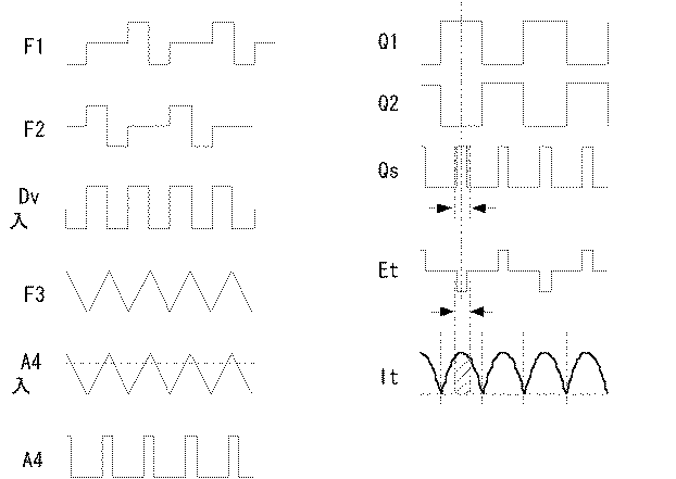
スイッチング手段のトランジスタQ1、Q2のエミッタは電流検出抵抗R4,R5を介してグラウンドと接続される。電流検出抵抗R4、R5は共振電流を検出する抵抗であり、増幅器A1、A2はこの抵抗に発生する電圧を検出するものである。F1、F2は検出された電圧を成型し、合成された波形は三角波発生回路F3と分周回路Dvに供給される。分周回路Dvで分周された電圧によってトランジスタQ1、Q2が駆動される。これにより、電流共振型の自励発振回路の構成を実現している。また、分周回路Dvにはマルチ・バイブレーターとしての機能を兼ねるようにすることで、電流共振型回路の起動手段とすることもできる。
FIG. 5 is an equivalent circuit diagram showing still another embodiment of the present invention.
The emitters of the transistors Q1 and Q2 of the switching means are connected to the ground via current detection resistors R4 and R5. The current detection resistors R4 and R5 are resistors for detecting a resonance current, and the amplifiers A1 and A2 are for detecting a voltage generated in the resistors. F1 and F2 shape the detected voltage, and the synthesized waveform is supplied to the triangular wave generating circuit F3 and the frequency dividing circuit Dv. The transistors Q1 and Q2 are driven by the voltage divided by the frequency dividing circuit Dv. Thus, the configuration of a current resonance type self-excited oscillation circuit is realized. Further, by making the frequency dividing circuit Dv also function as a multivibrator, it can be used as a starting means of a current resonance type circuit.
一方、放電管の管電流はエラー・アンプA3に帰還された後に増幅され、比較器A4で三角波と比較されることによりスイッチング手段Qsのスイッチング信号を生成している。図6に制御回路の各部の波形が示されている。スイッチング手段のトランジスタQ1、Q2のスイッチングは昇圧トランスT1の一次巻線に流れる電流Itがゼロになるタイミングで行われるために、電流位相とトランジスタQ1、O2のスイッチング信号の位相は均しい。 On the other hand, the tube current of the discharge tube is amplified after being fed back to the error amplifier A3, and is compared with a triangular wave by the comparator A4 to generate a switching signal of the switching means Qs. FIG. 6 shows waveforms at various parts of the control circuit. Since the switching of the transistors Q1 and Q2 of the switching means is performed at a timing when the current It flowing in the primary winding of the step-up transformer T1 becomes zero, the current phase and the phase of the switching signal of the transistors Q1 and O2 are equal.
他方、スイッチング手段Qsのスイッチングは、昇圧トランスT1に流れる電流のピークから見て対称になるように行われる。したがって、昇圧トランスT1の一次巻線にかかる電圧の位相は電流の位相と均しくなり、力率が改善される。
On the other hand, switching of the switching means Qs is performed so as to be symmetric when viewed from the peak of the current flowing through the step-up transformer T1. Therefore, the phase of the voltage applied to the primary winding of the step-up transformer T1 becomes equal to the phase of the current, and the power factor is improved.
図7は同期発振回路を内蔵した一例であって、電流共振型回路の起動手段を兼ねるとともに、検出された電流の波形を整形し、出力波形を一定間隔に揃える働きをするものである。この同期発振回路は共振引き込み型、弛張発振型、PLL型などいずれでも良い。 FIG. 7 shows an example in which a synchronous oscillation circuit is incorporated, which also serves as a starting means for the current resonance type circuit, and functions to shape the detected current waveform and align the output waveform at a constant interval. This synchronous oscillation circuit may be any of a resonance pull-in type, a relaxation oscillation type, a PLL type, and the like.
(作用)
次に、電流共振型の駆動手段がなぜインバータ回路に高効率をもたらすかについての一般論について述べる。
図8は、昇圧トランスの一次側駆動回路までを含めた二次側共振回路の等価回路であり、冷陰極管用インバータ回路における昇圧トランスと冷陰極管との関係を示している。この等価回路において、昇圧トランスは三端子等価回路で表わされている。米国の特許第6114814−B1号、第6,633,138号や第6,259,615号、及び特開2002−233158号ではこれをtank circuitと称し、特開昭59−032370号の共振回路及び本発明の発明者による特許第2733817号(米国特許第5495405号)、及び、特開2003−168585においては共振回路と称しているものであるが、いずれも同じものを意味するものである。
(Function)
Next, a general theory about why the current resonance type driving means brings high efficiency to the inverter circuit will be described.
FIG. 8 is an equivalent circuit of the secondary side resonance circuit including the primary side drive circuit of the step-up transformer, and shows the relationship between the step-up transformer and the cold cathode tube in the inverter circuit for the cold cathode tube. In this equivalent circuit, the step-up transformer is represented by a three-terminal equivalent circuit. In US Pat. Nos. 6,114,814-B1, 6,633,138 and 6,259,615, and Japanese Patent Laid-Open No. 2002-233158, this is referred to as a tank circuit, and a resonant circuit disclosed in Japanese Patent Laid-Open No. 59-032370. In Japanese Patent No. 2733817 (US Pat. No. 5,495,405) and Japanese Patent Application Laid-Open No. 2003-168585 by the inventor of the present invention, these are referred to as resonance circuits, and both mean the same thing.
この図において、C1は一次側のカップリング・コンデンサであり、電流共振型回路においては直流をカットする目的で、或いは、駆動手段がフル・ブリッジ(H-Bridge)回路である場合にはスイッチングのアンバランスによる直流成分をカットするために必要に応じて挿入されるものである。冷陰極管用のインバータ回路においては一般的には十分に大きな値を有することで共振に関与させない方が良い。これは熱陰極管用の電流共振型インバータ回路と技術思想が異なる。なお、カップリング・コンデンサC1を共振に関与させた場合にはインバータ回路の発熱が多くなり変換効率が低下する。 In this figure, C1 is a coupling capacitor on the primary side. In the current resonance type circuit, for the purpose of cutting direct current, or when the driving means is a full bridge (H-Bridge) circuit, switching is performed. It is inserted as necessary to cut the DC component due to unbalance. In general, an inverter circuit for a cold cathode tube should have a sufficiently large value so that it does not participate in resonance. This is different in technical idea from a current resonance type inverter circuit for a hot cathode tube. If the coupling capacitor C1 is involved in resonance, the inverter circuit generates more heat and the conversion efficiency decreases.
Leはトランスの漏れインダクタンス(学会)であり、JIS測定法による漏れインダクタンス(JIS)Lsとは区別される。Mはトランスの相互インダクタンスである。Cwは二次巻線の分布容量、Caは共振周波数の調整のために適宜付加される共振容量、Csは放電管周辺に発生する寄生容量で、これらは合成されて二次側の共振容量を構成するものであり、Zは放電管のインピーダンスである。 Le is the leakage inductance of the transformer (academic society) and is distinguished from the leakage inductance (JIS) Ls by the JIS measurement method. M is the mutual inductance of the transformer. Cw is a distributed capacity of the secondary winding, Ca is a resonant capacity that is appropriately added to adjust the resonance frequency, Cs is a parasitic capacity generated around the discharge tube, and these are combined to obtain the secondary side resonant capacity. Z is the impedance of the discharge tube.
参考までに、トランスの巻線の自己インダクタンスをLo、結合係数をkとすると、これらの数値の間には次の関係がある。
Le=k・Lo
M=(1−k)・Lo
Le = k ・ Lo
M = (1−k) ・ Lo
この等価回路を用いて回路シミュレーションを行うと次のような結果が得られる。
図9において、横軸はインバータ回路の駆動周波数を表し、図9の上図はトランス一次側から見た電圧と電流の位相特性を示した図であり、図9の下図は放電管のインピーダンスZに与えられる電圧の伝達特性を表したものである。この図の中で、放電管のインピーダンスZは3段階に変化させている。aがインピーダンス高、bがインピーダンス中、cがインピーダンス低の場合である。
When a circuit simulation is performed using this equivalent circuit, the following results are obtained.
9, the horizontal axis represents the drive frequency of the inverter circuit, the upper diagram in FIG. 9 is a diagram showing the phase characteristics of voltage and current viewed from the primary side of the transformer, and the lower diagram in FIG. 9 is the impedance Z of the discharge tube. It represents the transfer characteristic of the voltage given to. In this figure, the impedance Z of the discharge tube is changed in three stages. This is the case where a is high impedance, b is impedance, and c is low impedance.
熱陰極管の点灯回路として一般的に用いられるハーフ・ブリッジ型の電流共振型回路は共振回路が負荷と直列であって、定常放電時には負荷に対する昇圧作用を持たない。一方、冷陰極管を駆動する場合には、二次側の共振回路はParallel loaded serial resonance回路になるために、定常放電時でも負荷に対する昇圧作用を持つ。この場合、図9の上図において、位相特性とゼロ度の線が交差した周波数において、インバータ回路の駆動周波数は決定される。 A half-bridge type current resonance circuit generally used as a lighting circuit for a hot cathode tube has a resonance circuit in series with a load and does not have a boosting action on the load during steady discharge. On the other hand, when driving a cold-cathode tube, the secondary-side resonance circuit becomes a parallel loaded serial resonance circuit, and thus has a boosting action on the load even during steady discharge. In this case, in the upper diagram of FIG. 9, the drive frequency of the inverter circuit is determined at the frequency at which the phase characteristic and the zero degree line intersect.
放電管のインピーダンスZを高、中、低と変化させた場合の位相特性を見ると、共振回路のインピーダンスに比べて放電管のインピーダンスが低くなるに従い、図9の上図で示されるように、図8の検出手段1で検出される電流位相は共振電流の位相よりも遅れることになり、インバータ回路の発振周波数は共振回路の共振周波数よりも低い周波数で発振することになる。そして、インピーダンス小の場合にはゼロ度と交わる周波数がなくなってしまう。これは、ある限界を超えて放電管のインピーダンスZが小さくなると、この電流共振型インバータ回路においては発振の継続が不可能になることを示している。 Looking at the phase characteristics when the impedance Z of the discharge tube is changed to high, medium, and low, as the impedance of the discharge tube becomes lower than the impedance of the resonant circuit, as shown in the upper diagram of FIG. The current phase detected by the detection means 1 in FIG. 8 is delayed from the phase of the resonance current, and the oscillation frequency of the inverter circuit oscillates at a frequency lower than the resonance frequency of the resonance circuit. When the impedance is small, the frequency that intersects with zero degrees disappears. This indicates that if the impedance Z of the discharge tube is reduced beyond a certain limit, oscillation cannot be continued in this current resonance type inverter circuit.
放電管のインピーダンスが低い場合、これは共振回路のQ値が低いということである。すなわち、本発明においてはQが低い状態では回路の発振は継続できないことになる。したがって本発明において、Qの高い条件で構成することは必須の要件となる。 If the impedance of the discharge tube is low, this means that the Q value of the resonant circuit is low. In other words, in the present invention, circuit oscillation cannot be continued when Q is low. Therefore, in the present invention, it is an indispensable requirement to configure under a high Q condition.
一方、逆にQ値が高いことは本発明においては有利に働く。つまり、Qが高いほど二次側回路の共振電流が大きくなり、電流共振型回路の発振が安定するからである。また、Qが高いことは昇圧トランスの昇圧比も高くなることを意味する。 On the other hand, a high Q value is advantageous in the present invention. That is, the higher the Q is, the larger the resonance current of the secondary side circuit becomes, and the oscillation of the current resonance type circuit becomes stable. In addition, a high Q means that the step-up transformer has a high step-up ratio.
具体的にQの高い共振回路を構成するためには昇圧トランスの二次巻線を、従来の他励型駆動手段の場合の値よりも少なくするとともに、二次側の容量成分の値を大きく設定する。漏れインダクタンスの値は二次巻線の巻数の二乗に比例するために、わずかに巻数を減らすだけで漏れインダクタンスの値は大きく低下する。その結果、必要な電圧を得るための変成比を小さくすることができるので昇圧トランスのさらなる小型化が可能となる。 Specifically, in order to configure a resonant circuit with high Q, the secondary winding of the step-up transformer is made smaller than the value in the case of the conventional separately-excited drive means, and the value of the secondary side capacitance component is increased. Set. Since the value of the leakage inductance is proportional to the square of the number of turns of the secondary winding, the value of the leakage inductance is greatly reduced by slightly reducing the number of turns. As a result, the transformation ratio for obtaining the necessary voltage can be reduced, and the step-up transformer can be further downsized.
次に、本発明の電流共振型の回路と電力制御手段との関係を説明すると以下のようになる。
図5の回路において、各スイッチング手段のスイッチング・タイミングを見たものが図10である。図10は本実施例における各スイッチング手段のタイミングと電流を示す説明図である。スイッチング手段Qsのスイッチング・タイミングはトランジスタQ1及びQ2と同期し、トランジスタQ1、Q2に流れる電流の位相と昇圧トランスT1の一次巻線に与えられる電圧の位相が均しくなるようにスイッチングされる。この場合、昇圧トランスT1のセンタータップに流れる電流はItのようになる。
Next, the relationship between the current resonance type circuit of the present invention and the power control means will be described as follows.
FIG. 10 shows the switching timing of each switching means in the circuit of FIG. FIG. 10 is an explanatory diagram showing the timing and current of each switching means in the present embodiment. The switching timing of the switching means Qs is synchronized with the transistors Q1 and Q2, and is switched so that the phase of the current flowing through the transistors Q1 and Q2 is equal to the phase of the voltage applied to the primary winding of the step-up transformer T1. In this case, the current flowing through the center tap of the step-up transformer T1 is as It.
より詳しく見ると、bのタイミング、即ち、スイッチング手段QsがONの場合においては、図11のスイッチング手段QsがONの場合の電流の流れを示す等価回路図に示すように、スイッチング手段Qsを通じて昇圧トランスT1へと電流が流れる。 More specifically, when the timing of b, that is, when the switching means Qs is ON, as shown in the equivalent circuit diagram showing the flow of current when the switching means Qs of FIG. 11 is ON, the voltage is boosted through the switching means Qs. Current flows to transformer T1.
次に、図10のCのタイミングにおいて、スイッチング手段QsがOFFになると、電流は図12のスイッチング手段QsがOFFの場合の電流の流れを示す等価回路図に示すようにフライホイール・ダイオードDsを通じて流れるようになる。 Next, when the switching means Qs is turned OFF at the timing of C in FIG. 10, the current flows through the flywheel diode Ds as shown in the equivalent circuit diagram showing the current flow when the switching means Qs in FIG. 12 is OFF. It begins to flow.
この場合に流れる電流は単純ではない。図12に示した電流はあくまでも模式的に示したものであって、実際の昇圧トランスの一次巻線にはしばしば大きな振動電流が乗ることがある。 The current flowing in this case is not simple. The current shown in FIG. 12 is merely a schematic illustration, and a large oscillating current is often applied to the primary winding of an actual step-up transformer.
図13は図10のCのタイミングにおける電流の振動の様子を表した図である。
この振動電流の原因は後述するが、本発明においては、このような振動電流が発生した場合、図14のスイッチング手段Qs がOFFの場合に現れる振動電流を電源に回生するものである。図14の等価回路図に示すように、振動が起きるとスイッチング手段Qsを通じて逆方向の電流が流れ、この電流は回生ダイオードDrを通じて電源に回生する。
FIG. 13 is a diagram showing the state of current oscillation at the timing C in FIG.
Although the cause of this oscillating current will be described later, in the present invention, when such an oscillating current is generated, the oscillating current that appears when the switching means Qs in FIG. 14 is OFF is regenerated to the power source. As shown in the equivalent circuit diagram of FIG. 14, when vibration occurs, a reverse current flows through the switching means Qs, and this current is regenerated to the power source through the regenerative diode Dr.
つまり、順方向に流れる共振電流に対しては昇圧トランスT1の一次巻線をショートしたと同じ状態にして、共振電流のエネルギーを損失しないようにしている。一方、逆方向に流れる振動電流に対しては、これを電源に回生し、振動のエネルギーをダンプしているものである。 In other words, the resonance current flowing in the forward direction is set to the same state as when the primary winding of the step-up transformer T1 is short-circuited so that the energy of the resonance current is not lost. On the other hand, the oscillating current flowing in the reverse direction is regenerated to the power source to dump the vibration energy.
従来のDC−DCコンバータを用いた調光回路においては、このような回生電流のみを選択的にダンプする手段がなく、振動電流のエネルギーが蓄積されるので、一次巻線には不所望な電流振動が現れる。 In the dimming circuit using the conventional DC-DC converter, there is no means for selectively dumping only the regenerative current, and the energy of the oscillating current is accumulated. Vibration appears.
次に、このような振動電流がなぜ発生するかについて説明する。
冷陰極管用の昇圧トランスのように巻数が多く、高電圧を発生させるようなトランスの二次巻線上には多くの共振が存在する。これを一次巻線側からインピーダンス・アナライザで測定すると、図15のようになる。図15は高電圧用昇圧トランスの二次巻線上には多くの自己共振が存在することを示す説明図である。図15のZはトランスの一次巻線側からインピーダンス特性を測ったものであるが、複数の共振が見られる。このような寄生振動が発生する原因は、昇圧トランスの二次巻線が分布定数状になっているためであり、冷陰極管用インバータ回路のトランスなど、高圧用トランスの二次巻線上に発生する様々な寄生振動が原因である。
Next, why such an oscillating current is generated will be described.
There are many resonances on the secondary winding of a transformer that has a large number of turns and generates a high voltage, such as a step-up transformer for a cold cathode tube. When this is measured from the primary winding side by an impedance analyzer, it is as shown in FIG. FIG. 15 is an explanatory diagram showing that many self-resonances exist on the secondary winding of the high-voltage step-up transformer. Z in FIG. 15 is obtained by measuring the impedance characteristics from the primary winding side of the transformer, but a plurality of resonances are observed. The cause of such parasitic vibration is that the secondary winding of the step-up transformer has a distributed constant shape, and is generated on the secondary winding of the high-voltage transformer such as a transformer of a cold cathode tube inverter circuit. It is caused by various parasitic vibrations.
この図15において、Aの共振は一般的に良く知られるトランスの自己共振と呼ばれるものである。しかし、トランスには一般的にあまり知られてないがB,C,Dの自己共振も存在する。このうちのBの共振はエネルギーも大きく、一次巻線側に電流振動となって現れることがある。このような電流振動は特開昭56−88678号などにも「不所望な共振」として開示されている。 In FIG. 15, the resonance of A is generally known as the self-resonance of the transformer. However, although not generally known in transformers, there are also B, C, and D self-resonances. Of these, the resonance of B has large energy and may appear as current oscillation on the primary winding side. Such current oscillation is disclosed as “undesired resonance” in Japanese Patent Laid-Open No. 56-88678.
図16は、実際の冷陰極管用昇圧トランスの一次巻線に発生する振動電流の様子を示す説明図である。その説明図から、一次巻線を流れる電流は理想的な正弦波ではなく、高次数の不所望な共振電流が重乗されていることがわかる。インバータ回路の駆動周波数の整数倍の周波数と図16に示す高次共振の周波数とが一致した場合に不所望な電流の共振現象が顕著になる。 FIG. 16 is an explanatory diagram showing a state of an oscillating current generated in the primary winding of the actual step-up transformer for a cold cathode tube. From the explanatory diagram, it can be seen that the current flowing through the primary winding is not an ideal sine wave but is superimposed with an undesired high-order resonance current. When the frequency that is an integral multiple of the drive frequency of the inverter circuit matches the frequency of the higher-order resonance shown in FIG.
このような不所望な共振はトランジスタQ1、Q2のスイッチング・タイミングに悪影響を与える。特に、特開昭59−032370号、米国特許第6,633,138号、特開平8−288080号などに開示されるようなゼロ電流を検出してスイッチング・タイミングを決めるゼロ電流スイッチング手段による回路は深刻な影響を受ける。したがって、前述のような回生手段を用いて振動電流をダンプすることは有効である。 Such unwanted resonance adversely affects the switching timing of the transistors Q1 and Q2. In particular, a circuit using zero current switching means for detecting the zero current and determining the switching timing as disclosed in JP-A-59-032370, US Pat. No. 6,633,138, JP-A-8-288080, etc. Is severely affected. Therefore, it is effective to dump the oscillating current using the regenerative means as described above.
以上の作用に関する説明は、スイッチング手段Qsのスイッチング・タイミングをトランジスタQ1及びQ2と同期した場合について述べたが、トランジスタQ1、Q2に流れる電流とのスイッチング手段Qsのスイッチング・タイミングが非同期の場合においても同じ作用・効果を生じさせることが可能である。 Although the description regarding the above operation has been described about the case where the switching timing of the switching means Qs is synchronized with the transistors Q1 and Q2, even when the switching timing of the switching means Qs with the current flowing through the transistors Q1 and Q2 is asynchronous. It is possible to produce the same action / effect.
Claims (2)
該Q値が1ないし1をわずかに上回る値を超えた値においてもインバータ回路の動作周波数と二次側回路の共振周波数とがほぼ一致することにより、高い昇圧比を得て該放電管を点灯せしめるとともに、該昇圧トランス一次巻線側から見た電圧に対する電流の位相差が概ね少なくなることを特徴とする放電管用インバータ回路。
The current resonance type inverter circuit for a discharge tube has a step-up transformer, the primary winding of the step-up transformer has a center tap, the center tap is connected to a power source , and the other two terminals of the primary winding are respectively is connected to the collector of the two transistors, the emitter of the transistor is connected to a respective terminal of the primary winding of a current transformer having a center tap, the center tap of the current transformer is connected to ground, of the current transformer, respectively The primary side driving means configured to detect and oscillate a resonance current by detecting the emitter current of the transistor by connecting the secondary winding to the bases of the two transistors. The secondary circuit of the step-up transformer has a small leakage inductance value, and the secondary circuit Conductive tube is connected, the secondary side circuit of the step-up transformer having a distributed capacitance of the step-up transformer, and a capacitor which is suitably added in order to adjust the resonance frequency, the parasitic capacitance generated around the discharge tube, these capacitance components are combined to constitute a secondary side capacitance, the said secondary side capacitance and the small leakage inductance constitute a series resonance circuit, the discharge tube is connected in parallel with the capacitive component By constructing the series resonant circuit with a high Q value slightly exceeding Q 1 to 1 ,
Even when the Q value exceeds a value slightly exceeding 1 to 1, the operating frequency of the inverter circuit and the resonance frequency of the secondary side circuit substantially coincide with each other , thereby obtaining a high step-up ratio and lighting the discharge tube. allowed to together, the discharge tube inverter circuit, wherein substantially less Kunar that the phase difference between the current with respect to voltage seen from the step-up transformer primary winding.
前記トランジスタのエミッタに接続される電流トランスを電流検出抵抗に置き換えてエミッタとGNDとの間に配置し、該電流検出抵抗に流れる電流を検知し、該電流検出抵抗に発生する電圧は増幅器によって増幅され、該増幅された電圧は整形されて、前記昇圧トランスに流れる電流のピークから見て対称になるように、該トランジスタのスイッチング・タイミングを得ることにより、該昇圧トランス一次巻線側から見た電圧に対する電流の位相差が概ね少なくなることを特徴とする放電管用インバータ回路。 The inverter circuit for a current resonance type discharge tube according to claim 1,
The current transformer connected to the emitter of the transistor is replaced with a current detection resistor and is arranged between the emitter and GND, the current flowing through the current detection resistor is detected, and the voltage generated in the current detection resistor is amplified by an amplifier. The amplified voltage is shaped and viewed from the step-up transformer primary winding side by obtaining the switching timing of the transistor so that it is symmetrical as seen from the peak of the current flowing through the step-up transformer. discharge tube inverter circuit, wherein substantially less Kunar that the phase difference between the current with respect to voltage.
Priority Applications (6)
| Application Number | Priority Date | Filing Date | Title |
|---|---|---|---|
| JP2004318059A JP5048920B2 (en) | 2004-11-01 | 2004-11-01 | Current resonance type inverter circuit and power control means |
| KR1020050101852A KR20060052267A (en) | 2004-11-01 | 2005-10-27 | A current resonant inverter circuit and means for controlling power |
| CNA2005101188108A CN1802059A (en) | 2004-11-01 | 2005-10-31 | Current resonance type inverter circuit and power controlling method |
| TW094138093A TW200616495A (en) | 2004-11-01 | 2005-10-31 | Inverter circuit for discharge lamp and power controlling method |
| US11/261,492 US7453216B2 (en) | 2004-11-01 | 2005-10-31 | Current resonance type inverter circuit and power controlling method |
| EP05256722A EP1653786A3 (en) | 2004-11-01 | 2005-10-31 | Current resonance type inverter circuit and power controlling method |
Applications Claiming Priority (1)
| Application Number | Priority Date | Filing Date | Title |
|---|---|---|---|
| JP2004318059A JP5048920B2 (en) | 2004-11-01 | 2004-11-01 | Current resonance type inverter circuit and power control means |
Publications (2)
| Publication Number | Publication Date |
|---|---|
| JP2006129669A JP2006129669A (en) | 2006-05-18 |
| JP5048920B2 true JP5048920B2 (en) | 2012-10-17 |
Family
ID=35708962
Family Applications (1)
| Application Number | Title | Priority Date | Filing Date |
|---|---|---|---|
| JP2004318059A Expired - Fee Related JP5048920B2 (en) | 2004-11-01 | 2004-11-01 | Current resonance type inverter circuit and power control means |
Country Status (6)
| Country | Link |
|---|---|
| US (1) | US7453216B2 (en) |
| EP (1) | EP1653786A3 (en) |
| JP (1) | JP5048920B2 (en) |
| KR (1) | KR20060052267A (en) |
| CN (1) | CN1802059A (en) |
| TW (1) | TW200616495A (en) |
Families Citing this family (21)
| Publication number | Priority date | Publication date | Assignee | Title |
|---|---|---|---|---|
| JP2005312284A (en) * | 2005-01-12 | 2005-11-04 | Masakazu Ushijima | Inverter circuit for current resonance discharge tube |
| JP4908760B2 (en) | 2005-01-12 | 2012-04-04 | 昌和 牛嶋 | Current resonance type inverter circuit |
| CN1832321B (en) * | 2005-03-07 | 2011-09-14 | 柏怡国际股份有限公司 | Transverter |
| JP2008159545A (en) * | 2006-12-26 | 2008-07-10 | Sanken Electric Co Ltd | Cold-cathode tube fluorescent lamp inverter device |
| JP2008251339A (en) * | 2007-03-30 | 2008-10-16 | Sony Corp | Fluorescent tube driving method, and its device |
| JP2008287979A (en) * | 2007-05-16 | 2008-11-27 | Minebea Co Ltd | Discharge lamp lighting device |
| CN101272098B (en) * | 2008-04-08 | 2010-11-03 | 广州金升阳科技有限公司 | Twin-triode current control type self-oscillation flyback converter |
| JP5149686B2 (en) * | 2008-04-24 | 2013-02-20 | パナソニック株式会社 | Power conversion device, discharge lamp lighting device using the same, and vehicle headlamp device |
| CN101568216B (en) * | 2008-04-25 | 2012-09-26 | 群康科技(深圳)有限公司 | Inverter circuit and liquid crystal display device |
| WO2009139077A1 (en) * | 2008-05-15 | 2009-11-19 | 国立大学法人 東京工業大学 | Alternating voltage control unit |
| US9413314B2 (en) | 2009-05-08 | 2016-08-09 | Federal-Mogul Ignition Company | Corona ignition with self-tuning power amplifier |
| KR101657972B1 (en) * | 2009-05-08 | 2016-09-20 | 페더럴-모굴 이그니션 컴퍼니 | Corona ignition with self-tuning power amplifier |
| US8289734B2 (en) * | 2009-10-15 | 2012-10-16 | Ansaldo Sts Usa, Inc. | Output apparatus to output a vital output from two sources |
| CN102291001B (en) * | 2011-08-26 | 2014-01-01 | 广州金升阳科技有限公司 | Self-excitation push-pull type converter |
| US20130200798A1 (en) * | 2012-02-07 | 2013-08-08 | Laurence P. Sadwick | Fluorescent Lamp Dimmer |
| JP6005502B2 (en) * | 2012-12-18 | 2016-10-12 | 新電元工業株式会社 | Power supply |
| TWI641290B (en) * | 2013-02-06 | 2018-11-11 | 英諾系統公司 | Fluorescent lamp dimmer |
| DE112015000373T5 (en) * | 2014-01-10 | 2016-10-06 | Murata Manufacturing Co., Ltd. | High Voltage Power Supply |
| TWI556203B (en) * | 2015-01-30 | 2016-11-01 | 友達光電股份有限公司 | Display device and converter control method |
| CN106329977B (en) * | 2015-07-03 | 2018-10-09 | 台达电子工业股份有限公司 | The control method of inverter circuit |
| TWI777412B (en) * | 2020-06-29 | 2022-09-11 | 立錡科技股份有限公司 | Resonant half-bridge flyback power converter and primary controller circuit and control method thereof |
Family Cites Families (22)
| Publication number | Priority date | Publication date | Assignee | Title |
|---|---|---|---|---|
| JPS5688678A (en) | 1979-12-19 | 1981-07-18 | Toshiba Electric Equip Corp | Transistor inverter |
| JPS5932370A (en) | 1982-08-16 | 1984-02-21 | Hitachi Ltd | High-voltage power supply device |
| JPS6024190U (en) * | 1983-07-20 | 1985-02-19 | 富士電気化学株式会社 | Push-pull converter bias prevention circuit |
| JPH06125513A (en) * | 1992-10-13 | 1994-05-06 | Sharp Corp | Power source circuit for television receiver |
| US5382882A (en) | 1993-04-20 | 1995-01-17 | General Electric Company | Power supply circuit for a gas discharge lamp |
| JP2733817B2 (en) | 1993-08-30 | 1998-03-30 | 昌和 牛嶋 | Inverter circuit for discharge tube |
| JPH07211472A (en) | 1994-01-24 | 1995-08-11 | Hitachi Media Electron:Kk | Lighting device |
| JP3443654B2 (en) * | 1994-11-24 | 2003-09-08 | ミネベア株式会社 | Voltage resonance type inverter circuit |
| JP3292788B2 (en) * | 1995-03-29 | 2002-06-17 | 昌和 牛嶋 | Inverter circuit for discharge tube |
| JP3547837B2 (en) * | 1995-03-31 | 2004-07-28 | ミネベア株式会社 | Inverter device |
| JPH08288080A (en) | 1995-04-17 | 1996-11-01 | Nakano Denki Seisakusho:Kk | Discharge lamp lighting device |
| JP3273161B2 (en) * | 1996-06-11 | 2002-04-08 | シャープ株式会社 | Load drive circuit |
| US6081439A (en) * | 1996-06-19 | 2000-06-27 | Kijima Co., Ltd. | Inverter provided with output regulating mechanism |
| US5619106A (en) * | 1996-06-24 | 1997-04-08 | General Electric Company | Diodeless start circiut for gas discharge lamp having a voltage divider connected across the switching element of the inverter |
| JPH11215826A (en) * | 1998-01-21 | 1999-08-06 | Hitachi Ltd | Self oscillation-type current resonance converter |
| US6114814A (en) | 1998-12-11 | 2000-09-05 | Monolithic Power Systems, Inc. | Apparatus for controlling a discharge lamp in a backlighted display |
| JP2002233158A (en) | 1999-11-09 | 2002-08-16 | O2 Micro Internatl Ltd | High-efficiency adaptive dc-to-ac converter |
| US6259615B1 (en) | 1999-07-22 | 2001-07-10 | O2 Micro International Limited | High-efficiency adaptive DC/AC converter |
| JP3705966B2 (en) * | 1999-09-07 | 2005-10-12 | 東光株式会社 | Switching power supply circuit |
| TW515224B (en) * | 2001-03-07 | 2002-12-21 | Ambit Microsystems Corp | Inverter and lamp ignition system using the same |
| US6570344B2 (en) * | 2001-05-07 | 2003-05-27 | O2Micro International Limited | Lamp grounding and leakage current detection system |
| JP4267883B2 (en) | 2001-09-21 | 2009-05-27 | ミネベア株式会社 | LCD display unit |
-
2004
- 2004-11-01 JP JP2004318059A patent/JP5048920B2/en not_active Expired - Fee Related
-
2005
- 2005-10-27 KR KR1020050101852A patent/KR20060052267A/en not_active Application Discontinuation
- 2005-10-31 CN CNA2005101188108A patent/CN1802059A/en active Pending
- 2005-10-31 US US11/261,492 patent/US7453216B2/en not_active Expired - Fee Related
- 2005-10-31 EP EP05256722A patent/EP1653786A3/en not_active Withdrawn
- 2005-10-31 TW TW094138093A patent/TW200616495A/en not_active IP Right Cessation
Also Published As
| Publication number | Publication date |
|---|---|
| TW200616495A (en) | 2006-05-16 |
| CN1802059A (en) | 2006-07-12 |
| EP1653786A2 (en) | 2006-05-03 |
| EP1653786A3 (en) | 2008-07-09 |
| KR20060052267A (en) | 2006-05-19 |
| US20060164024A1 (en) | 2006-07-27 |
| US7453216B2 (en) | 2008-11-18 |
| JP2006129669A (en) | 2006-05-18 |
| TWI312261B (en) | 2009-07-11 |
Similar Documents
| Publication | Publication Date | Title |
|---|---|---|
| JP5048920B2 (en) | Current resonance type inverter circuit and power control means | |
| JP4908760B2 (en) | Current resonance type inverter circuit | |
| KR101217372B1 (en) | An inverter circuit for current resonance electric discharge lamp | |
| JP2003520407A (en) | Power feedback power factor correction scheme for multiple lamp operation. | |
| JPH08506931A (en) | Electronic ballast with two transistors and two transformers | |
| JPH05508965A (en) | Circuit for driving gas discharge lamp loads | |
| WO2013026267A1 (en) | Self-excited push-pull converter | |
| JP2008153198A (en) | Current driven toroid-free feedback type ballast | |
| JP4526488B2 (en) | Inverter circuit for current resonance type discharge tube | |
| JP2003235259A (en) | Switching power circuit | |
| JP4993548B2 (en) | Self-excited inverter drive circuit | |
| WO2007052514A1 (en) | Discharge lamp lighting apparatus | |
| CN108124341B (en) | LED driver and LED lighting device | |
| JP4462262B2 (en) | Switching power supply circuit | |
| JP2007288823A (en) | Switching power supply circuit | |
| JP2008067533A (en) | Switching power supply circuit | |
| JPH08103076A (en) | Switching power supply circuit | |
| JP2001136745A (en) | Switching power supply circuit | |
| JP2812649B2 (en) | Inverter circuit | |
| JP2003070257A (en) | Inverter unit | |
| JP2006269137A (en) | Inverter circuit for inorganic el element | |
| JP2000348892A (en) | Discharge lamp lighting device | |
| JPH0538151A (en) | Resonance power circuit | |
| JP2003257691A (en) | Discharge lamp lighting device | |
| JP2002300784A (en) | Power supply device, discharge lamp lighting device and laminaire |
Legal Events
| Date | Code | Title | Description |
|---|---|---|---|
| A621 | Written request for application examination |
Free format text: JAPANESE INTERMEDIATE CODE: A621 Effective date: 20071003 |
|
| A977 | Report on retrieval |
Free format text: JAPANESE INTERMEDIATE CODE: A971007 Effective date: 20100607 |
|
| A131 | Notification of reasons for refusal |
Free format text: JAPANESE INTERMEDIATE CODE: A131 Effective date: 20110118 |
|
| A601 | Written request for extension of time |
Free format text: JAPANESE INTERMEDIATE CODE: A601 Effective date: 20110405 |
|
| A602 | Written permission of extension of time |
Free format text: JAPANESE INTERMEDIATE CODE: A602 Effective date: 20110412 |
|
| A601 | Written request for extension of time |
Free format text: JAPANESE INTERMEDIATE CODE: A601 Effective date: 20110502 |
|
| A602 | Written permission of extension of time |
Free format text: JAPANESE INTERMEDIATE CODE: A602 Effective date: 20110511 |
|
| A601 | Written request for extension of time |
Free format text: JAPANESE INTERMEDIATE CODE: A601 Effective date: 20110609 |
|
| A602 | Written permission of extension of time |
Free format text: JAPANESE INTERMEDIATE CODE: A602 Effective date: 20110614 |
|
| A521 | Written amendment |
Free format text: JAPANESE INTERMEDIATE CODE: A523 Effective date: 20110715 |
|
| A131 | Notification of reasons for refusal |
Free format text: JAPANESE INTERMEDIATE CODE: A131 Effective date: 20120110 |
|
| A601 | Written request for extension of time |
Free format text: JAPANESE INTERMEDIATE CODE: A601 Effective date: 20120326 |
|
| A602 | Written permission of extension of time |
Free format text: JAPANESE INTERMEDIATE CODE: A602 Effective date: 20120402 |
|
| A601 | Written request for extension of time |
Free format text: JAPANESE INTERMEDIATE CODE: A601 Effective date: 20120501 |
|
| A602 | Written permission of extension of time |
Free format text: JAPANESE INTERMEDIATE CODE: A602 Effective date: 20120508 |
|
| A521 | Written amendment |
Free format text: JAPANESE INTERMEDIATE CODE: A523 Effective date: 20120529 |
|
| TRDD | Decision of grant or rejection written | ||
| A01 | Written decision to grant a patent or to grant a registration (utility model) |
Free format text: JAPANESE INTERMEDIATE CODE: A01 Effective date: 20120710 |
|
| A01 | Written decision to grant a patent or to grant a registration (utility model) |
Free format text: JAPANESE INTERMEDIATE CODE: A01 |
|
| A61 | First payment of annual fees (during grant procedure) |
Free format text: JAPANESE INTERMEDIATE CODE: A61 Effective date: 20120720 |
|
| FPAY | Renewal fee payment (event date is renewal date of database) |
Free format text: PAYMENT UNTIL: 20150727 Year of fee payment: 3 |
|
| R150 | Certificate of patent or registration of utility model |
Free format text: JAPANESE INTERMEDIATE CODE: R150 |
|
| LAPS | Cancellation because of no payment of annual fees |