JP4954413B2 - Thin gate oxide decoupling capacitor - Google Patents
Thin gate oxide decoupling capacitor Download PDFInfo
- Publication number
- JP4954413B2 JP4954413B2 JP2001547425A JP2001547425A JP4954413B2 JP 4954413 B2 JP4954413 B2 JP 4954413B2 JP 2001547425 A JP2001547425 A JP 2001547425A JP 2001547425 A JP2001547425 A JP 2001547425A JP 4954413 B2 JP4954413 B2 JP 4954413B2
- Authority
- JP
- Japan
- Prior art keywords
- diffusion region
- conductor
- capacitor
- diffusion
- decoupling capacitor
- Prior art date
- Legal status (The legal status is an assumption and is not a legal conclusion. Google has not performed a legal analysis and makes no representation as to the accuracy of the status listed.)
- Expired - Fee Related
Links
- 239000003990 capacitor Substances 0.000 title claims description 93
- 238000009792 diffusion process Methods 0.000 claims description 47
- 239000004065 semiconductor Substances 0.000 claims description 24
- 239000004020 conductor Substances 0.000 claims description 23
- 239000000758 substrate Substances 0.000 claims description 15
- 239000012212 insulator Substances 0.000 claims description 11
- 238000009825 accumulation Methods 0.000 description 23
- 235000001892 vitamin D2 Nutrition 0.000 description 11
- 230000004044 response Effects 0.000 description 10
- 239000000969 carrier Substances 0.000 description 7
- 238000005516 engineering process Methods 0.000 description 7
- 238000000034 method Methods 0.000 description 5
- 230000008569 process Effects 0.000 description 5
- 230000008859 change Effects 0.000 description 4
- 238000013461 design Methods 0.000 description 4
- 229910044991 metal oxide Inorganic materials 0.000 description 4
- 150000004706 metal oxides Chemical class 0.000 description 4
- 230000009467 reduction Effects 0.000 description 3
- 230000008901 benefit Effects 0.000 description 2
- 238000010586 diagram Methods 0.000 description 2
- 230000000694 effects Effects 0.000 description 2
- 230000005669 field effect Effects 0.000 description 2
- 239000002184 metal Substances 0.000 description 2
- 238000012986 modification Methods 0.000 description 2
- 230000004048 modification Effects 0.000 description 2
- 229910021420 polycrystalline silicon Inorganic materials 0.000 description 2
- 229920005591 polysilicon Polymers 0.000 description 2
- 238000005215 recombination Methods 0.000 description 2
- 230000006798 recombination Effects 0.000 description 2
- 238000004891 communication Methods 0.000 description 1
- 230000000052 comparative effect Effects 0.000 description 1
- 238000011161 development Methods 0.000 description 1
- 238000006073 displacement reaction Methods 0.000 description 1
- 230000008713 feedback mechanism Effects 0.000 description 1
- 230000014509 gene expression Effects 0.000 description 1
- 230000010354 integration Effects 0.000 description 1
- 239000000463 material Substances 0.000 description 1
- 238000012545 processing Methods 0.000 description 1
- 229910052710 silicon Inorganic materials 0.000 description 1
- 239000010703 silicon Substances 0.000 description 1
- 230000005641 tunneling Effects 0.000 description 1
- MECHNRXZTMCUDQ-RKHKHRCZSA-N vitamin D2 Chemical compound C1(/[C@@H]2CC[C@@H]([C@]2(CCC1)C)[C@H](C)/C=C/[C@H](C)C(C)C)=C\C=C1\C[C@@H](O)CCC1=C MECHNRXZTMCUDQ-RKHKHRCZSA-N 0.000 description 1
- 239000011653 vitamin D2 Substances 0.000 description 1
Images


Classifications
-
- H—ELECTRICITY
- H01—ELECTRIC ELEMENTS
- H01L—SEMICONDUCTOR DEVICES NOT COVERED BY CLASS H10
- H01L29/00—Semiconductor devices adapted for rectifying, amplifying, oscillating or switching, or capacitors or resistors with at least one potential-jump barrier or surface barrier, e.g. PN junction depletion layer or carrier concentration layer; Details of semiconductor bodies or of electrodes thereof ; Multistep manufacturing processes therefor
-
- H—ELECTRICITY
- H01—ELECTRIC ELEMENTS
- H01L—SEMICONDUCTOR DEVICES NOT COVERED BY CLASS H10
- H01L27/00—Devices consisting of a plurality of semiconductor or other solid-state components formed in or on a common substrate
- H01L27/02—Devices consisting of a plurality of semiconductor or other solid-state components formed in or on a common substrate including semiconductor components specially adapted for rectifying, oscillating, amplifying or switching and having at least one potential-jump barrier or surface barrier; including integrated passive circuit elements with at least one potential-jump barrier or surface barrier
- H01L27/04—Devices consisting of a plurality of semiconductor or other solid-state components formed in or on a common substrate including semiconductor components specially adapted for rectifying, oscillating, amplifying or switching and having at least one potential-jump barrier or surface barrier; including integrated passive circuit elements with at least one potential-jump barrier or surface barrier the substrate being a semiconductor body
- H01L27/08—Devices consisting of a plurality of semiconductor or other solid-state components formed in or on a common substrate including semiconductor components specially adapted for rectifying, oscillating, amplifying or switching and having at least one potential-jump barrier or surface barrier; including integrated passive circuit elements with at least one potential-jump barrier or surface barrier the substrate being a semiconductor body including only semiconductor components of a single kind
- H01L27/0805—Capacitors only
-
- H—ELECTRICITY
- H01—ELECTRIC ELEMENTS
- H01L—SEMICONDUCTOR DEVICES NOT COVERED BY CLASS H10
- H01L29/00—Semiconductor devices adapted for rectifying, amplifying, oscillating or switching, or capacitors or resistors with at least one potential-jump barrier or surface barrier, e.g. PN junction depletion layer or carrier concentration layer; Details of semiconductor bodies or of electrodes thereof ; Multistep manufacturing processes therefor
- H01L29/66—Types of semiconductor device ; Multistep manufacturing processes therefor
- H01L29/86—Types of semiconductor device ; Multistep manufacturing processes therefor controllable only by variation of the electric current supplied, or only the electric potential applied, to one or more of the electrodes carrying the current to be rectified, amplified, oscillated or switched
- H01L29/92—Capacitors with potential-jump barrier or surface barrier
- H01L29/94—Metal-insulator-semiconductors, e.g. MOS
-
- H—ELECTRICITY
- H01—ELECTRIC ELEMENTS
- H01L—SEMICONDUCTOR DEVICES NOT COVERED BY CLASS H10
- H01L2924/00—Indexing scheme for arrangements or methods for connecting or disconnecting semiconductor or solid-state bodies as covered by H01L24/00
- H01L2924/0001—Technical content checked by a classifier
- H01L2924/0002—Not covered by any one of groups H01L24/00, H01L24/00 and H01L2224/00
Description
【0001】
(発明の背景)
(発明の技術分野)
本発明は集積回路に関し、より具体的には、集積回路のデカップリング・キャパシタに関する。
【0002】
(背景技術)
デカップリング・キャパシタ(「デキャップ」)は、雑音の遮断のために集積回路(IC)に使用されている。実際、これらは、ほほすべてのICに多用されている。半導体キャパシタの一つのタイプは、MOS−Cまたは金属酸化膜半導体キャパシタと呼ばれる。MOS−Cは、(ゲート酸化膜など少なくとも絶縁体を含む)誘電体領域によって分離された2個の端子を有する。端子の1つはゲートであり、他の1つはボデー(およびおそらくソース拡散およびドレイン拡散)である。半導体キャパシタのもう一つのタイプは、n−チャネル金属酸化膜半導体FET(NMOSFET)またはp−チャネル金属酸化膜半導体FET(NMOSFET)などの電界効果トランジスタ(FET)を使用している。端子の一つはゲートであり、他の端子はソース、ドレイン、およびボデーである。端子は、(ゲート酸化膜など少なくとも絶縁体を含む)誘電体によって分離されている。MOS−CとFETキャパシタの違いは、FETでは、ソースおよびドレインがボデーと異なる極性タイプを有することである。MOS−Cでは、ソース拡散/ドレイン拡散(存在する場合)は、ボデーと同じ極性を有する。集積回路でのキャパシタの挙動は、R.Pierret等「Field Effect Devices」(Addison−Wesley、第2版、1990年)47〜59頁、およびN.Weste等「Principles of CMOS VLSI Design」(Addison−Wesley、第2版、1993年)180〜82頁に記載されている。
【0003】
高誘電率絶縁体によって2本の金属線を間に挟んだキャパシタなど、その他のデカップリング・キャパシタも可能である。しかし、今日のMOS技術での材料の課題および集積は非常に難しい。
【0004】
キャパシタのキャパシタンスCは、式C=_A/dによって与えられ、但し_は誘電率、Aは面積、dは距離である。ICの設計では、部品の寸法を小さくすることが望ましい。したがって、数年来、キャパシタの面積Aは縮小しており、一方、電極間の距離dもまた短縮された。現在使用されているキャパシタ構造は、漏洩のない酸化膜を用いることによって概して動作は良好である。現在のデカップリング・キャパシタ構造は、MOS−Cを反転に保つように電圧を印加することによって、単位面積あたり最大のキャパシタンス値と、良好な高周波応答時間と、低い直列抵抗とを得る。プロセス技術のスケーリングに伴って、トランジスタの良好な駆動電流能力および良好な短チャネル効果を維持するために、ゲート酸化膜の厚みもスケーリングさせる。ゲート酸化膜がスケーリングを続けると(例えば、30A未満へ)、このキャパシタ構造は酸化膜を通して著しい漏洩伝導を引き起こすことになる(例えば、高いトンネル漏洩)。
【0005】
(概要)
いくつかの実施態様では、本発明は、電源電圧を伝える第1導体および接地電圧を伝える第2導体を有するダイを含む。空乏モードで動作する半導体キャパシタが第1導体と第2導体の間にデカップリング・キャパシタンスを形成するために第1導体と第2導体の間に結合される。この半導体キャパシタはゲート電圧を有する。
【0006】
n−ボデー内のn+ゲート・ポリおよびn+ソース/ドレイン領域;n−ボデー内のp+ゲート・ポリおよびn+ソース/ドレイン領域;n−ボデー内のp+ゲート・ポリおよびp+ソース/ドレイン領域;p−ボデー内のp+ゲート・ポリおよびp+ソース/ドレイン領域;p−ボデー内のn+ゲート・ポリおよびp+ソース/ドレイン領域;p−ボデー内のn+ゲート・ポリおよびn+ソース/ドレイン領域を含めた様々な構造を用いることができる。電源電圧は、フラットバンド電圧より大きな絶対値を有することができる。
【0007】
さらなる実施形態を説明し特許を請求する。
【0008】
本発明は、下記の詳細な説明から、および本発明の実施形態に付随する図面から、さらに完全に理解されるであろう。しかし、これらは、説明した特定の実施形態に本発明を限定するものではなく単に説明および理解のためである。
【0009】
(詳細な説明)
本発明は、半導体キャパシタ(トランジスタまたはMOS−C)を空乏モードで動作させて、絶縁体(例えば、ゲート酸化膜)中の漏洩を低減させることに係る。空乏モードでの動作は面積あたりのキャパシタンスを低下させるので、これは直観に反するものである。キャパシタンスのこの低下を補うために、面積を拡大することができるが、それは望ましくない。本発明を生み出す際に、本発明者らは、空乏モードで動作させることによってキャリアの数が低減し、したがってゲート酸化膜内のトンネリングの量が低減し、漏洩も低減することに気が付いた。
【0010】
一般的な考え方では、反転モードで動作するMOSトランジスタ構造に由来するMOS−Cキャパシタを使用しない方向である。代替案は、空乏モードで動作する絶縁体として、ゲート酸化膜を用いたキャパシタ構造の使用である。有効キャパシタンスは約25%(概算値)低下するが、一方、約1Vの電源技術について漏洩はほぼ100分の1に低減する。キャパシタは空乏モードでバイアスするので(蓄積領域近くへ)、キャパシタンスの低下はC−V曲線で観察できる。漏洩の低減は、ゲート酸化膜下の空乏チャネルには薄いゲート酸化膜を通り抜けるキャリアが少ないという事実による。こうしたキャパシタのQファクタは、反転のMOSトランジスタ・キャップに類似しているであろう。少数キャリアの発生および再結合に依存しないで、デキャップにかさねるAC信号に応答する必要のあるキャリアを供給する場合は特にそうである。デキャップを通しての漏洩を一桁より大きく低減させる必要がある場合は、やや大きな面積のキャパシタを使用することによって、低下したキャパシタンスをいつでも補うことができる。
【0011】
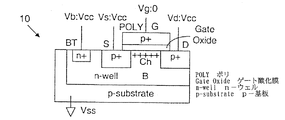
n−ボデーを有するデカップリング・キャパシタ
図1を参照すると、従来技術のPMOSトランジスタ・キャパシタ10は、p−基板、n−ウェル、p+ソースS、p+ドレインD、p+ポリシリコン・ゲート電極(ポリ)G、およびボデーBのn+ボデー・タップBTを含む。本開示の専門用語によれば、トランジスタ・キャパシタ10は、n−ボデー(n−ウェル)上p+/p+キャップと呼ばれる。但し、第1のp+はポリ・タイプの意味であり、第2のp+はS/D領域のタイプを意味する。なお、キャパシタ構造の場合、1つの拡散領域をソース、他方をドレインと呼ぶことは特に意味のあることではないが、学術用語の便宜上そうしている。なお、ソース拡散/ドレイン拡散は、本発明のすべての実施形態で必要というわけではないが、しかし、これは直列抵抗を低下させてRC周波数応答に役立つこともある。ゲート酸化膜の直下が表面12である。ゲート酸化膜の表面の下がチャネルChである。本開示では、トランジスタではないMOC−C構造の場合でも、この領域をチャネルと呼ぶ。トランジスタ・キャパシタ10には以下のように電圧を印加する。ボデー電圧Vbは電源電圧Vcc(ある場合はVddと呼ぶ)であり、ソース電圧およびドレイン電圧VsおよびVdはどちらもVccであり、ゲート電圧VGとp−基板はどちらも接地されている(Vssまたは0と呼ぶ)。基板は、下、上、またはその他から接地することができる。図1では、VgはVssに接続されている。しかし、いくつかの実施形態では、GはVssに接続されず、非ゼロおよび非Vcc値の可能性がある。
【0012】
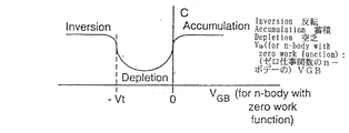
図2は、ポリとボデーが同じタイプを有するためにゼロ仕事関数のn−ボデー(例えば、n−ウェル)キャパシタ構造の、キャパシタンス対ゲート・ツー・ボデー電圧VGB曲線を示す。なお、ドレイン電圧とソース電圧は、ボデー電圧と同じでもよい。この曲線は、一般の関係を示すことだけを意図しており、正確な値または形を示すものではない。実際の曲線は少し違って見えることがある。さらに、曲線の形は、異なる周波数で変化する可能性がある。明らかなように、キャパシタンスは、蓄積と反転で高く、空乏で低い。Vtがしきい値電圧である。一般に、蓄積モード、空乏モード、反転モードの境界は厳密ではないかもしれないが、蓄積モードは0<VGBの場合に起こり、空乏モードは−Vt<VGB<0の場合に起こり、反転モードはVGB<−Vtの場合に起こる。
【0013】
図3は、ポリとボデーが異なるタイプを有するために非ゼロ仕事関数(非ゼロ・フラット・バンド電圧VFB)のn−ボデーキャパシタ構造の、キャパシタンス対ゲート・ツー・ボデー電圧VGB曲線を示す。この曲線は、一般の関係を示すことだけを意図しており、正確な値または形を示すものではない。実際の曲線は少し違って見えることがある。さらに、曲線の形は、異なる周波数で変化する可能性がある。明らかなように、キャパシタンスは、蓄積および反転で高く、空乏で低い。高濃度でドープされたポリのVFBは約1.0ボルトである。一般に、蓄積モード、空乏モード、反転モードの境界は厳密ではないかもしれないが、蓄積モードはVFB<VGBの場合に起こり、空乏モードは−Vt<VGB<VFBの場合に起こり、反転モードはVGB<−Vtの場合に起こる。なお、−Vtと0の間、0とVFBの間、0とVtの間の相対的距離は、VBGまたはVtの実際の値を制約するものではなく、これらは実施形態ごとに異なる可能性がある。
【0014】
図1の従来技術トランジスタ・キャパシタ10の場合について考えると、n−ボデーがあり、ポリおよびボデーが異なるタイプを有し、したがって非ゼロ仕事関数があるので、図3の曲線が当てはまる。この構造のフラットバンド電圧(VFB)は約1Vである。図1の場合には、VGB=−Vccであり、これは−Vtよりもさらに負である。したがって、トランジスタ・キャパシタ10は、反転モードである(より具体的には、チャネルがボデーの反対タイプであるホールを含むので、このチャネルは反転である)。したがって、これは、単位面積あたりキャパシタンスが非常に高く(おそらく最大)、周波数応答が非常に良好で、直列抵抗が低い。しかし、これには、ゲート酸化膜を通る漏洩も見られ、特に薄いゲート酸化膜では高い(おそらく最大)。Vccは、このデキャップ構造ではVtより高くするべきである。なお、(変位電流に対する)このキャップの、周波数および直列抵抗の関数としてのキャパシタンスが、このデキャップのQファクタを表す。なお、p+ポリ・ゲートおよびn−ボデーなので、反転のPMOSキャップのフラットバンド電圧(VFB)は約1V(非ゼロ)である。
【0015】
図4は、本発明のいくつかの実施形態によるMOS−C 40を示す。なお、用語MOS(金属酸化膜半導体)は広い解釈を意図している。すなわち、金属がどんな特別のタイプの導体にも限定されず(すなわち、ポリシリコンである必要はなく)、絶縁体が酸化膜である必要はなく、半導体部分は特別のタイプの構造に限定されない。MOS−C 40は、上記の命名法によればn−ボデー上n+/n+と示される(すなわち、ポリがn+、S/Dがn+である)。VgはVccであり、S/D/Bは0(Vss)である。n−ウェルが用いられ、ポリとボデーが同じタイプを有するので、図2の曲線が当てはまる。MOS−C 40のVFBは0Vである。VGB=Vccであり、したがってMOS−C 40は蓄積モードにある(チャネルには、ボデーと同じタイプの電子が蓄積される)。図4の構造では、デザイン・ツールでこうしたレイアウト(n−ウェル上にn−ポリを描く)にすることが望ましいかもしれない。MOS−C 40はすべてのVcc値で動作する。これは、単位面積あたりのキャパシタンスが高く(良好)、漏洩はやや低い。これは、周波数応答が良好で、直列抵抗が低い。
【0016】
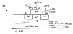
図5は、本発明のいくつかの実施形態によるMOS−C 50を示す。MOS−C 50は、上記の命名法によればn−ボデー上p+/n+と示される。VgはVccであり、S/D/Bは0(Vss)である。n−ウェルが用いられ、ポリとボデーが異なるタイプを有するので、図3の曲線が当てはまる。MOS−C 50のVFBは約1Vである。VGB=Vccである。Vcc>VFBの場合は、MOS−C 50は蓄積モードにあり(チャネル蓄積)、MOS−C<VFBの場合は、MOS−C 50は空乏モードにある(チャネル空乏)。Vcc=VFBの場合は、モードは蓄積モードと空乏モードの間である。本発明のいくつかの実施形態では、VccはVFBより小さく、したがってMOS−C 50は空乏モードにあり、漏洩は低減するであろう。この構造は特別のレイアウトを必要とするかもしれない。MOS−C 50は、単位面積あたりのキャパシタンスが低いが、空乏モードのため(漏れるキャリアが少ない)漏洩は著しく低い。これは、周波数応答は良好であるが、直列抵抗が高い可能性がある。なお、この構造は埋め込みチャネルMOSトランジスタ構造に似ている。
【0017】
図6は、本発明のいくつかの実施形態によるPMOSトランジスタ・キャパシタ60MOS−C 60を示す。トランジスタ・キャパシタ60は、上記の命名法によればn−ボデー上p+/p+と示される。VgはVccであり、S/D/Bは0(Vss)である(図1の反対)。n−ウェルが用いられ、ポリとボデーが異なるタイプを有するので、図3の曲線が当てはまる。MOS−C 50のVFBは約1Vである。VGB=Vccである。Vcc>VFBの場合は、MOS−C 60は蓄積モードにあり(チャネル蓄積)、MOS−C<VFBの場合は、MOS−C 60は空乏モードにある(チャネル空乏)。本発明のいくつかの実施形態では、VccはVFBより小さく、したがってMOS−C 60は空乏モードにあり、漏洩は低減するであろう。MOS−C 60は、単位面積あたりのキャパシタンスが低減しているが、空乏モードのため(漏れるキャリアが少ない)漏洩は著しく低減している。しかし、周波数応答および直列抵抗が問題かもしれない。
【0018】
p−ポリを有するデカップリング・キャパシタ
p−ボデー(p−ウェルまたはp−基板)を有するトランジスタおよびMOS−Cキャパシタの構造の例を以下に説明する。なお、p−ウェルが示されているが、ボデーはp−基板だけのこともある。さらに、基板は、p−ウェルを有するn−タイプもありうる。
【0019】
図7は、ポリとボデーが同じタイプを有するためにゼロ仕事関数を有するp−ボデー・キャパシタ構造の、キャパシタンス対ゲート・ツー・ボデー電圧VGB曲線を示す。この曲線は、一般の関係を示すことのみを意図しており、正確な値または形を示すものではない。実際の曲線は少し違って見えることがある。さらに、曲線の形は、異なる周波数で変化する可能性がある。明らかなように、キャパシタンスは、蓄積および反転で高く、空乏で低い。一般に、蓄積モード、空乏モード、反転モードの境界は厳密ではないかもしれないが、蓄積モードはVGB<0の場合に起こり、空乏モードは0<VGB<Vtの場合に起こり、反転モードはVGB>Vtの場合に起こる。
【0020】
図8は、ポリとボデーが異なるタイプを有するために非ゼロ仕事関数(非ゼロ・フラット・バンド電圧VFB)のp−ボデー・キャパシタ構造の、キャパシタンス対ゲート・ツー・ボデー電圧VGB曲線を示す。この曲線は、一般の関係を示すことのみを意図しており、正確な値または形を示すものではない。実際の曲線は少し違って見えることがある。さらに、曲線の形は、異なる周波数で変化する可能性がある。明らかなように、キャパシタンスは、蓄積および反転で高く、空乏で低い。高濃度でドープされたポリのVFBは、約1.0ボルトである(これは、曲線の負領域にあるが)。一般に、蓄積モード、空乏モード、反転モードの境界は厳密ではないかもしれないが、蓄積モードはVGB<−VFB(例えば、−1V)の場合に起こり、空乏モードは−VFB<VGB<Vtの場合に起こり、反転モードはVt<VGBの場合に起こる。なお、−VFBと0の間、および0とVtの間の相対的距離は、VFBまたはVtの実際の値を制約するものではなく、これらは実施形態ごとに異なる可能性がある。
【0021】
図9は、従来技術のNMOSトランジスタ・キャパシタ90を示し、上記の命名法によれば、p−ボデー上n+/n+で示される。この場合、これはp−ボデーすなわちp−基板であるが、n−基板上のp−ウェルまたはp−基板内のp−ウェルでもよい。Vg=Vccであり、S/D/Bは0(Vss)である。ポリとボデーが異なるタイプを有するので、図8の曲線が用いられる。VGB=Vccである。曲線8で、VccはVtより大きく、したがって、トランジスタ・キャパシタ90は反転モード(チャネルが反転)で動作している。デキャップ90は、トリプル・ウェル・プロセスを必要とせず、特別のレイアウト要求を用いない。これは、単位面積あたりのキャパシタンスが非常に高く(多分最大)、周波数応答が非常に良好で、直列抵抗が低い。主な問題は、ゲート酸化膜、特に薄いゲート酸化膜からの漏洩もまた多い(多分最大)ことである。このデキャップ構造については、VccはVtより大きくするべきである。
【0022】
図10は、上記命名法によればp−ボデー上p+/p+を有するMOS−Cキャパシタ100を示す。p−ウェルが示されているが、これは必要ではない。Vg=0(Vss)であり、S/D/B=Vccである。ポリとボデーが同じタイプなので、図7の曲線が当てはまる。VGB=−Vccであり、したがって、キャパシタ100は蓄積モードにある(チャネルに蓄積される)。いくつかの実施形態では、キャパシタ100は、p−ウェルとp−基板の間にn−ボデーまたは他の絶縁体を含む。目的は、Vcc電圧が基板または他のボデーの電圧に与える影響を防止することである。このトリプル・ウェル・プロセスは、デザイン・ツールに追加のレイアウト(P−ウェル上にP−ポリを描く)を必要とするかもしれない。デキャップ100はすべてのVcc値で動作する。これは、単位面積あたりのキャパシタンスが高く(良好)、漏洩はやや少ない。これは、周波数応答が良好で、直列抵抗が低い。
【0023】
図11は、上記命名法によればp−ボデー上n+/p+を有するMOS−Cキャパシタ110を示す。p−ウェルが示されているがこれは必要ではない。Vg=0(Vss)であり、S/D/B=Vccである。ポリとボデーが異なるタイプなので、図8の曲線が当てはまる。VGB=−Vccである。Vcc>VFB(−Vcc<−VFB)の場合は、キャパシタ110は蓄積モードにある(チャネルに蓄積される)。Vcc<VFB(−Vcc>−VFB)の場合は、キャパシタ110は空乏モードにある(チャネルは空乏である)。いくつかの実施形態では、漏洩の役に立つように空乏モードを用いる。いくつかの実施形態では、キャパシタ110は、p−ウェルとp−基板の間にn−ボデーまたは他の絶縁体を含む。キャパシタ110は、単位面積あたりのキャパシタンスが低く、かつ漏洩が著しく低い。これは、周波数応答は良好であるが、直列抵抗が高い。
【0024】
図12は、上記命名法によればp−ボデー上n+/n+を有するNMOSトランジスタ120を示す。p−ウェルが示されているがこれは必要ではない。Vg=0(Vss)であり、S/D/B=Vccである。ポリとボデーが異なるタイプなので、図8の曲線が当てはまる。VGB=−Vccである。Vcc>VFB(−Vcc<−VFB)の場合は、キャパシタ120は蓄積モードにある(チャネルに蓄積される)。Vcc<VFB(−Vcc>−VFB)の場合は、キャパシタ120は空乏モードにある(チャネルは空乏である)。いくつかの実施形態では、漏洩の役に立つように空乏モードを用いる。いくつかの実施形態では、キャパシタ120は、p−ウェルとp−基板の間にn−ボデーまたは他の絶縁体を含む。この構造では漏洩は良好である(低減)。しかし、周波数応答および直列抵抗が問題になるかもしれない。この構造は、トリプル・ウェル・プロセスを必要とするかもしれない。
【0025】
下記の付録は、上記のキャパシタ、および本発明のいくつかの実施形態の範囲内の他のキャパシタの比較一覧表を提供する。
【0026】
他の情報および実施形態
図13は、本明細書記載の1つまたは複数の構造を含めたキャパシタ(例えば、キャパシタ134)が含まれるダイ130を示す。ダイ130は、マイクロプロセッサ、DSP(デジタル信号プロセッサ)、エンベディド・コントローラ、ASIC(特定用途向け集積回路)、およびコミュニケーション・チップを含めて、任意の様々なタイプの電気デバイスとすることができる。
【0027】
上記のように、いくつかの実施形態では、キャパシタを空乏モードとすることが望ましい。多くの状況では、キャパシタを蓄積モードまたは反転モードに接近させることも望ましいであろう。なお、図2、3、7、8において、空乏モードでは、蓄積モードまたは反転モードに向かって曲線は上向きである。ゲート電圧、ボデー電圧、ソース/ドレイン電圧、しきい値電圧、および/またはドーピング濃度を調節することによって、キャパシタンスを微調整することが可能である。図14を参照すると、ダイ140は、(その中に記載された1つまたは複数の様々なキャパシタを表す)キャパシタ134を含む。ダイ140は電圧回路142を含み、これが、1つまたは複数のボデー、ゲート、およびソース/ドレインに電圧を供給して、所望のキャパシタンス・レベルを実現することができる。ボデー電圧を変化させて、キャパシタに順方向または逆方向ボデー・バイアスを持たせることができる。なお、ボデー・バイアスが変化するとVtが変化する。所望のキャパシタンス・レベルを得るために、フィードバック機構があってもよい。
【0028】
単に一例としてであるが、いくつかの実施形態では、有効キャパシタンスを約25%低下させることができるが、一方約1Vの電源技術について、漏洩はほぼ100分の1に低減すると思われる。キャパシタは空乏モードでバイアスするので(蓄積領域近くへ)、キャパシタンスの低下はC−V曲線で観察できる。漏洩の低減は、ゲート酸化膜下の空乏チャネルには薄いゲート酸化膜を通り抜けるキャリアが少ないためである。こうしたキャパシタのQファクタは、反転のMOSトランジスタ・キャップに類似しているであろう。少数キャリアの発生および再結合に依存しないで、デキャップにかさねるAC信号に応答する必要のあるキャリアを供給する場合は特にそうである。デキャップを通しての漏洩を一桁より大きく低減させる必要がある場合は、やや大きな面積のキャパシタを使用することによって、低下したキャパシタンスを補うことができる。したがって、本発明は、さらなる供給電圧のスケーリング、ならびに低電圧、高性能、および低電力CMOS回路用のプロセス技術の開発を支持するものである。将来、ゲート酸化膜の厚みを、既にスケーリングされたトランジスタの要求に合わせてスケーリングしても、雑音遮蔽用のデキャップを、本発明者らが提案する構造を有する本発明者らのICに継続して利用することができる。本発明らが提案した解決法は、現在の加工技術と適合するものである。
【0029】
本発明は、SOI(シリコン・オン・インシュレータ)構造と接続して使用することができる。
【0030】
さらに、周知のように、電源電圧および接地電圧は必ずしも一定ではなく、雑音、負荷、または他の理由で変動がある。
【0031】
MOSFET以外のFETも使用できる。図示した実施形態はエンハンスメント・モード・トランジスタを含むが、当分野の技術者なら本開示の恩恵があれば明白な回路の改造を行うことによって、空乏モード・トランジスタも使用することができる。
【0032】
本明細書で「実施形態」、「一実施形態」、「いくつかの実施形態」、または「他の実施形態」と言及した場合は、実施形態に関して説明された特定の特徴、構造、または特性が、本発明の実施形態の必ずしもすべてではないが、本発明の実施形態の少なくともいくつかに含まれていることを意味する。様々な表現「実施形態」、「一実施形態」、または「いくつかの実施形態」は、必ずしもすべてが同じ実施形態に言及するものではない。
【0033】
本明細書が、部品、特徴、構造、または特性を含んでもよい(「may」、「might」、または「could」 be included)と言う場合は、その特定の部品、特徴、構造、または特性を含む必要はない。本明細書または特許請求の範囲が、「a」または「an」要素に言及する場合は、これは唯一の要素があることを意味していない。明細書または特許請求の範囲が「追加の(an additional)」要素に言及する場合、これは、2つ以上の追加の要素があることを排除しない。
【0034】
当技術分野の技術者なら本開示の恩恵があれば、上記説明および図面から、本発明の範囲内で多くの他の変形を行うことができることを理解するであろう。したがって、本発明の範囲を定義するのは、その任意の修正を含めて頭書の特許請求の範囲である。
【0035】
付録:いくつかの可能性を列挙した比較一覧表。これは、包括的であることを意図したものではない。他の可能性が存在する。情報のいくつかは単なる最高の推測である。
【表1】

【図面の簡単な説明】
【図1】 従来技術のキャパシタの概略横断面図である。
【図2】 ゼロ仕事関数のn−ボデーを有するキャパシタの、キャパシタンス対ゲート・ツー・ボデー電圧のグラフである。
【図3】 非ゼロ仕事関数のn−ボデーを有するキャパシタの、キャパシタンス対ゲート・ツー・ボデー電圧のグラフである。
【図4】 本発明のいくつかの実施形態によるキャパシタの概略横断面図である。
【図5】 本発明のいくつかの実施形態によるキャパシタの概略横断面図である。
【図6】 本発明のいくつかの実施形態によるキャパシタの概略横断面図である。
【図7】 ゼロ仕事関数のp−ボデーを有するキャパシタの、キャパシタンス対ゲート・ツー・ボデー電圧のグラフである。
【図8】 非ゼロ仕事関数のp−ボデーを有するキャパシタの、キャパシタンス対ゲート・ツー・ボデー電圧のグラフである。
【図9】 従来技術のキャパシタの概略横断面図である。
【図10】 本発明のいくつかの実施形態によるキャパシタの概略横断面図である。
【図11】 本発明のいくつかの実施形態によるキャパシタの概略横断面図である。
【図12】 本発明のいくつかの実施形態によるキャパシタの概略横断面図である。
【図13】 本発明のいくつかの実施形態によるキャパシタを有するダイのブロック図である。
【図14】 本発明のいくつかの実施形態によるキャパシタおよび電圧回路を有するダイのブロック図である。[0001]
(Background of the Invention)
(Technical field of the invention)
The present invention relates to integrated circuits, and more particularly to integrated circuit decoupling capacitors.
[0002]
(Background technology)
Decoupling capacitors (“decaps”) are used in integrated circuits (ICs) for noise rejection. In fact, these are widely used in almost all ICs. One type of semiconductor capacitor is called a MOS-C or metal oxide semiconductor capacitor. The MOS-C has two terminals separated by a dielectric region (including at least an insulator such as a gate oxide). One terminal is the gate and the other is the body (and possibly source and drain diffusions). Another type of semiconductor capacitor uses a field effect transistor (FET) such as an n-channel metal oxide semiconductor FET (NMOSFET) or a p-channel metal oxide semiconductor FET (NMOSFET). One of the terminals is a gate, and the other terminals are a source, a drain, and a body. The terminals are separated by a dielectric (including at least an insulator such as a gate oxide film). The difference between MOS-C and FET capacitors is that in FETs, the source and drain have a different polarity type than the body. In MOS-C, source diffusion / drain diffusion (if present) has the same polarity as the body. The behavior of capacitors in integrated circuits is Pierret et al., "Field Effect Devices" (Addison-Wesley, 2nd edition, 1990) 47-59; West et al., “Principles of CMOS VLSI Design” (Addison-Wesley, 2nd edition, 1993), pages 180-82.
[0003]
Other decoupling capacitors are also possible, such as a capacitor with two metal wires sandwiched between high dielectric constant insulators. However, material challenges and integration in today's MOS technology is very difficult.
[0004]
The capacitance C of the capacitor is given by the equation C = _A / d, where _ is the dielectric constant, A is the area, and d is the distance. In IC design, it is desirable to reduce component dimensions. Therefore, for several years, the area A of the capacitor has been reduced, while the distance d between the electrodes has also been reduced. Currently used capacitor structures generally perform well by using a leak-free oxide film. Current decoupling capacitor structures obtain maximum capacitance value per unit area, good high frequency response time, and low series resistance by applying a voltage to keep MOS-C inverted. As the process technology scales, the gate oxide thickness is also scaled to maintain the transistor's good drive current capability and good short channel effect. As the gate oxide continues to scale (eg, to less than 30A), this capacitor structure will cause significant leakage conduction through the oxide (eg, high tunnel leakage).
[0005]
(Overview)
In some embodiments, the present invention includes a die having a first conductor that carries a power supply voltage and a second conductor that carries a ground voltage. A semiconductor capacitor operating in a depletion mode is coupled between the first conductor and the second conductor to form a decoupling capacitance between the first conductor and the second conductor. This semiconductor capacitor has a gate voltage.
[0006]
n + gate poly and n + source / drain regions in n− body; p + gate poly and n + source / drain regions in n− body; p + gate poly and p + source / drain regions in n− body; p− P + gate poly and p + source / drain regions in the body; n + gate poly and p + source / drain regions in the p-body; various, including n + gate poly and n + source / drain regions in the p-body A structure can be used. The power supply voltage can have an absolute value greater than the flat band voltage.
[0007]
Further embodiments are described and claimed.
[0008]
The invention will be more fully understood from the following detailed description and from the drawings accompanying the embodiments of the invention. However, they are not intended to limit the invention to the particular embodiments described, but are merely for explanation and understanding.
[0009]
(Detailed explanation)
The present invention relates to operating a semiconductor capacitor (transistor or MOS-C) in a depletion mode to reduce leakage in an insulator (eg, a gate oxide film). This is counter-intuitive because operation in the depletion mode reduces the capacitance per area. To compensate for this drop in capacitance, the area can be increased, but this is undesirable. In creating the present invention, the inventors have realized that operating in the depletion mode reduces the number of carriers, thus reducing the amount of tunneling in the gate oxide and reducing leakage.
[0010]
The general idea is that the MOS-C capacitor derived from the MOS transistor structure operating in the inversion mode is not used. An alternative is the use of a capacitor structure with a gate oxide as the insulator operating in the depletion mode. The effective capacitance is reduced by approximately 25% (approximate), while the leakage is reduced by almost a factor of 100 for a power technology of about 1V. Since the capacitor is biased in the depletion mode (towards the storage region), the capacitance drop can be observed on the CV curve. The reduction in leakage is due to the fact that the depletion channel under the gate oxide has less carriers passing through the thin gate oxide. The Q factor of such a capacitor would be similar to an inverting MOS transistor cap. This is especially the case when supplying carriers that do not rely on minority carrier generation and recombination and need to respond to an AC signal that leads to decap. If leakage through the decap needs to be reduced by more than an order of magnitude, the reduced capacitance can always be compensated by using a slightly larger area capacitor.
[0011]
Decoupling capacitor with n-body
Referring to FIG. 1, the prior art
[0012]
FIG. 2 illustrates capacitance versus gate-to-body voltage V for a zero work function n-body (eg, n-well) capacitor structure because poly and body have the same type. GB A curve is shown. Note that the drain voltage and the source voltage may be the same as the body voltage. This curve is intended only to show a general relationship and not an exact value or shape. The actual curve may look a little different. Furthermore, the shape of the curve can change at different frequencies. As is apparent, the capacitance is high for accumulation and inversion and low for depletion. Vt is a threshold voltage. In general, the boundary between accumulation mode, depletion mode, and inversion mode may not be strict, but accumulation mode is 0 <V GB And the depletion mode is -Vt <V GB Occurs when <0 and the inversion mode is V GB Occurs when <−Vt.
[0013]
FIG. 3 shows that non-zero work function (non-zero flat band voltage V FB ) N-body capacitor structure, capacitance versus gate-to-body voltage V GB A curve is shown. This curve is intended only to show a general relationship and not an exact value or shape. The actual curve may look a little different. Furthermore, the shape of the curve can change at different frequencies. As is apparent, the capacitance is high with accumulation and inversion and low with depletion. Highly doped poly V FB Is about 1.0 volts. In general, the boundary between accumulation mode, depletion mode, and inversion mode may not be strict, but accumulation mode is V FB <V GB And the depletion mode is -Vt <V GB <V FB Occurs when the inversion mode is V GB Occurs when <−Vt. In addition, between -Vt and 0, 0 and V FB The relative distance between 0 and Vt is V BG Or it does not constrain the actual value of Vt, which may vary from embodiment to embodiment.
[0014]
Considering the case of the prior
[0015]
FIG. 4 illustrates a MOS-
[0016]
FIG. 5 illustrates a MOS-
[0017]
FIG. 6 illustrates a PMOS transistor capacitor 60MOS-
[0018]
Decoupling capacitor with p-poly
An example of the structure of a transistor having a p-body (p-well or p-substrate) and a MOS-C capacitor will be described below. Although a p-well is shown, the body may be only a p-substrate. Furthermore, the substrate may be n-type with a p-well.
[0019]
FIG. 7 shows the capacitance versus gate-to-body voltage V for a p-body capacitor structure with zero work function because the poly and body have the same type. GB A curve is shown. This curve is intended only to show a general relationship, not an exact value or shape. The actual curve may look a little different. Furthermore, the shape of the curve can change at different frequencies. As is apparent, the capacitance is high with accumulation and inversion and low with depletion. In general, the boundary between accumulation mode, depletion mode, and inversion mode may not be strict, but accumulation mode is V GB Occurs when <0, depletion mode is 0 <V GB Occurs when <Vt, the inversion mode is V GB Occurs when> Vt.
[0020]
FIG. 8 shows that non-zero work function (non-zero flat band voltage V FB ) P-body capacitor structure, capacitance versus gate-to-body voltage V GB A curve is shown. This curve is intended only to show a general relationship, not an exact value or shape. The actual curve may look a little different. Furthermore, the shape of the curve can change at different frequencies. As is apparent, the capacitance is high with accumulation and inversion and low with depletion. Highly doped poly V FB Is approximately 1.0 volts (although it is in the negative region of the curve). In general, the boundary between accumulation mode, depletion mode, and inversion mode may not be strict, but accumulation mode is V GB <-V FB (For example, -1V), and the depletion mode is -V FB <V GB Occurs when <Vt, the inversion mode is Vt <V GB Happens in the case of. -V FB The relative distance between 0 and 0 and 0 and Vt is V FB Or it does not constrain the actual value of Vt, which may vary from embodiment to embodiment.
[0021]
FIG. 9 shows a prior art
[0022]
FIG. 10 shows a MOS-
[0023]
FIG. 11 shows a MOS-
[0024]
FIG. 12 shows an
[0025]
The following appendix provides a comparative list of the above capacitors and other capacitors within the scope of some embodiments of the present invention.
[0026]
Other information and embodiments
FIG. 13 illustrates a die 130 that includes a capacitor (eg, capacitor 134) that includes one or more structures described herein. The die 130 can be any of various types of electrical devices including a microprocessor, a DSP (Digital Signal Processor), an embedded controller, an ASIC (Application Specific Integrated Circuit), and a communication chip.
[0027]
As noted above, in some embodiments it is desirable to place the capacitor in a depletion mode. In many situations, it may also be desirable to bring the capacitor closer to the accumulation mode or the inversion mode. 2, 3, 7, and 8, in the depletion mode, the curve is upward toward the accumulation mode or the inversion mode. The capacitance can be fine tuned by adjusting the gate voltage, body voltage, source / drain voltage, threshold voltage, and / or doping concentration. Referring to FIG. 14, die 140 includes a capacitor 134 (representing one or more various capacitors described therein). The
[0028]
By way of example only, in some embodiments, the effective capacitance can be reduced by about 25%, while for a power technology of about 1V, the leakage appears to be reduced by almost a factor of 100. Since the capacitor is biased in the depletion mode (towards the storage region), the capacitance drop can be observed on the CV curve. The reduction in leakage is due to the small number of carriers passing through the thin gate oxide film in the depletion channel under the gate oxide film. The Q factor of such a capacitor would be similar to an inverting MOS transistor cap. This is especially the case when supplying carriers that do not rely on minority carrier generation and recombination and need to respond to an AC signal that leads to decap. If leakage through the decap needs to be reduced by more than an order of magnitude, the reduced capacitance can be compensated by using a slightly larger area capacitor. The present invention therefore supports further supply voltage scaling and development of process technology for low voltage, high performance, and low power CMOS circuits. In the future, even if the gate oxide thickness is scaled to meet the requirements of already scaled transistors, noise shielding decap will continue to our IC with the structure we propose. Can be used. The solution proposed by the present inventors is compatible with current processing technology.
[0029]
The present invention can be used in connection with an SOI (Silicon On Insulator) structure.
[0030]
Furthermore, as is well known, the power supply voltage and the ground voltage are not necessarily constant and may vary due to noise, load, or other reasons.
[0031]
FETs other than MOSFETs can also be used. Although the illustrated embodiment includes an enhancement mode transistor, those skilled in the art can also use a depletion mode transistor by making obvious circuit modifications with the benefit of this disclosure.
[0032]
Any reference herein to “an embodiment”, “one embodiment”, “some embodiments”, or “other embodiments” refers to a particular feature, structure, or characteristic described with respect to the embodiment. Is not necessarily all of the embodiments of the present invention, but is included in at least some of the embodiments of the present invention. The various expressions “embodiments”, “one embodiment”, or “some embodiments” do not necessarily all refer to the same embodiments.
[0033]
Where this specification may refer to a part, feature, structure, or characteristic (“may”, “might”, or “cold” be included), that particular part, feature, structure, or characteristic It is not necessary to include. Where the specification or claims refer to an “a” or “an” element, this does not mean there is only one element. Where the specification or claims refer to “an additional” element, this does not exclude the presence of two or more additional elements.
[0034]
Those skilled in the art will appreciate from the foregoing description and drawings that many other variations may be made within the scope of the present invention, given the benefit of this disclosure. Accordingly, it is the following claims, including any modifications thereof, that define the scope of the invention.
[0035]
Appendix: Comparison table listing several possibilities. This is not intended to be comprehensive. There are other possibilities. Some of the information is just the best guess.
[Table 1]
[Brief description of the drawings]
FIG. 1 is a schematic cross-sectional view of a prior art capacitor.
FIG. 2 is a graph of capacitance versus gate-to-body voltage for a capacitor having a zero work function n-body.
FIG. 3 is a graph of capacitance versus gate-to-body voltage for a capacitor having a non-zero work function n-body.
FIG. 4 is a schematic cross-sectional view of a capacitor according to some embodiments of the invention.
FIG. 5 is a schematic cross-sectional view of a capacitor according to some embodiments of the invention.
FIG. 6 is a schematic cross-sectional view of a capacitor according to some embodiments of the invention.
FIG. 7 is a graph of capacitance versus gate-to-body voltage for a capacitor with zero work function p-body.
FIG. 8 is a graph of capacitance versus gate-to-body voltage for a capacitor with a non-zero work function p-body.
FIG. 9 is a schematic cross-sectional view of a prior art capacitor.
FIG. 10 is a schematic cross-sectional view of a capacitor according to some embodiments of the invention.
FIG. 11 is a schematic cross-sectional view of a capacitor according to some embodiments of the invention.
FIG. 12 is a schematic cross-sectional view of a capacitor according to some embodiments of the invention.
FIG. 13 is a block diagram of a die having a capacitor according to some embodiments of the invention.
FIG. 14 is a block diagram of a die having a capacitor and a voltage circuit according to some embodiments of the present invention.
Claims (16)
接地電圧を伝える第2導体と、そして
第1導体と第2導体の間でデカップリング・キャパシタンスを備えるための半導体デカップリング・キャパシタであって、空乏モードで動作するように構成された半導体デカップリング・キャパシタと
から構成されるダイにおいて、
前記半導体デカップリング・キャパシタは、
(a)電源電圧を受けるための前記第1導体に接続されたゲート電極と、
(b)接地電圧を受けるための前記第2導体に接続された拡散領域と、そして
(c)前記拡散領域を通じて前記接地電圧を受け、これによって前記半導体デカップリング・キャパシタは前記空乏モードになる、ボデーと
から成り、
前記拡散領域は第1拡散領域であり、前記半導体デカップリング・キャパシタはさらに前記接地電圧を受けるための前記第2導体に接続された第2拡散領域を有し、
前記ボデーは前記第1および第2拡散領域を通じて前記接地電圧を受け、そして
前記半導体デカップリング・キャパシタはフラットバンド電圧を有し、かつ前記電源電圧が前記フラットバンド電圧より小さい絶対値を有する
ことを特徴とするダイ。A first conductor for transmitting a power supply voltage;
A semiconductor decoupling capacitor configured to operate in a depletion mode, comprising: a second conductor for transmitting a ground voltage; and a semiconductor decoupling capacitor for providing a decoupling capacitance between the first conductor and the second conductor -In a die composed of capacitors,
The semiconductor decoupling capacitor is:
(A) a gate electrode connected to the first conductor for receiving a power supply voltage;
(B) a diffusion region connected to the second conductor for receiving a ground voltage; and (c) receiving the ground voltage through the diffusion region, whereby the semiconductor decoupling capacitor is in the depletion mode. Body and
The diffusion region is a first diffusion region, and the semiconductor decoupling capacitor further has a second diffusion region connected to the second conductor for receiving the ground voltage;
The body receives the ground voltage through the first and second diffusion regions ; and
The die according to claim 1, wherein the semiconductor decoupling capacitor has a flat band voltage and the power supply voltage has an absolute value smaller than the flat band voltage .
接地電圧を伝える第2導体と、そして
第1導体と第2導体の間にデカップリング・キャパシタンスを備えるための半導体デカップリング・キャパシタであって、空乏モードで動作するように構成された半導体デカップリング・キャパシタと
から構成されるダイであって、
前記半導体デカップリング・キャパシタは、
(a)接地電圧を受けるための前記第2導体に接続されたゲート電極と、
(b)電源電圧を受けるための前記第1導体に接続された拡散領域と、
(c)前記拡散領域を通じて前記電源電圧を受け、これによって前記半導体デカップリング・キャパシタは前記空乏モードになる、ボデーと、
(d)基板と、そして
(e)前記基板と前記ボデーの間にある絶縁体と
から構成され、
前記拡散領域は第1拡散領域であり、前記半導体デカップリング・キャパシタはさらに前記電源電圧を受けるための前記第1導体に接続された第2拡散領域を有し、
前記ボデーは前記第1および第2拡散領域を通じて前記電源電圧を受け、そして
前記半導体デカップリング・キャパシタはフラットバンド電圧を有し、かつ前記電源電圧が前記フラットバンド電圧より小さい絶対値を有する
ことを特徴とするダイ。A first conductor for transmitting a power supply voltage;
A semiconductor decoupling capacitor configured to operate in a depletion mode, comprising: a second conductor for transmitting a ground voltage; and a semiconductor decoupling capacitor for providing a decoupling capacitance between the first conductor and the second conductor A die composed of a capacitor,
The semiconductor decoupling capacitor is:
(A) a gate electrode connected to the second conductor for receiving a ground voltage;
(B) a diffusion region connected to the first conductor for receiving a power supply voltage;
(C) receiving the power supply voltage through the diffusion region, thereby causing the semiconductor decoupling capacitor to enter the depletion mode;
(D) a substrate, and (e) an insulator between the substrate and the body,
The diffusion region is a first diffusion region, and the semiconductor decoupling capacitor further has a second diffusion region connected to the first conductor for receiving the power supply voltage;
The body receives the power supply voltage through the first and second diffusion regions ; and
The die according to claim 1, wherein the semiconductor decoupling capacitor has a flat band voltage and the power supply voltage has an absolute value smaller than the flat band voltage .
Applications Claiming Priority (3)
| Application Number | Priority Date | Filing Date | Title |
|---|---|---|---|
| US09/469,406 | 1999-12-22 | ||
| US09/469,406 US6828638B2 (en) | 1999-12-22 | 1999-12-22 | Decoupling capacitors for thin gate oxides |
| PCT/US2000/031352 WO2001046989A2 (en) | 1999-12-22 | 2000-11-13 | Decoupling capacitors for thin gate oxides |
Publications (3)
| Publication Number | Publication Date |
|---|---|
| JP2004501501A JP2004501501A (en) | 2004-01-15 |
| JP2004501501A5 JP2004501501A5 (en) | 2008-02-14 |
| JP4954413B2 true JP4954413B2 (en) | 2012-06-13 |
Family
ID=23863664
Family Applications (1)
| Application Number | Title | Priority Date | Filing Date |
|---|---|---|---|
| JP2001547425A Expired - Fee Related JP4954413B2 (en) | 1999-12-22 | 2000-11-13 | Thin gate oxide decoupling capacitor |
Country Status (8)
| Country | Link |
|---|---|
| US (1) | US6828638B2 (en) |
| JP (1) | JP4954413B2 (en) |
| KR (1) | KR100532208B1 (en) |
| AU (1) | AU3072601A (en) |
| DE (1) | DE10085347B4 (en) |
| GB (1) | GB2374462B (en) |
| HK (1) | HK1046776B (en) |
| WO (1) | WO2001046989A2 (en) |
Families Citing this family (30)
| Publication number | Priority date | Publication date | Assignee | Title |
|---|---|---|---|---|
| US6828654B2 (en) * | 2001-12-27 | 2004-12-07 | Broadcom Corporation | Thick oxide P-gate NMOS capacitor for use in a phase-locked loop circuit and method of making same |
| US6917544B2 (en) | 2002-07-10 | 2005-07-12 | Saifun Semiconductors Ltd. | Multiple use memory chip |
| US6809386B2 (en) * | 2002-08-29 | 2004-10-26 | Micron Technology, Inc. | Cascode I/O driver with improved ESD operation |
| US7136304B2 (en) | 2002-10-29 | 2006-11-14 | Saifun Semiconductor Ltd | Method, system and circuit for programming a non-volatile memory array |
| US7178004B2 (en) | 2003-01-31 | 2007-02-13 | Yan Polansky | Memory array programming circuit and a method for using the circuit |
| JP4046634B2 (en) * | 2003-04-08 | 2008-02-13 | Necエレクトロニクス株式会社 | Voltage-controlled capacitance element and semiconductor integrated circuit |
| WO2005013475A1 (en) * | 2003-08-05 | 2005-02-10 | Toyo Communication Equipment Co., Ltd. | Piezo-oscillator |
| JP2005175003A (en) * | 2003-12-08 | 2005-06-30 | Matsushita Electric Ind Co Ltd | Decoupling capacitor and semiconductor integrated circuit |
| DE102004006484A1 (en) * | 2004-02-10 | 2005-08-25 | Infineon Technologies Ag | Integrated circuit with electrostatic discharge (ESD) resistant capacitor located in N-trough, with certain polarity of capacitor permitting formation depletion zone in trough and high ESD strength of capacitor |
| US7256438B2 (en) * | 2004-06-08 | 2007-08-14 | Saifun Semiconductors Ltd | MOS capacitor with reduced parasitic capacitance |
| WO2006037376A1 (en) * | 2004-10-06 | 2006-04-13 | Freescale Semiconductor, Inc | A varactor |
| US7638850B2 (en) | 2004-10-14 | 2009-12-29 | Saifun Semiconductors Ltd. | Non-volatile memory structure and method of fabrication |
| US8053812B2 (en) | 2005-03-17 | 2011-11-08 | Spansion Israel Ltd | Contact in planar NROM technology |
| JP2007027760A (en) | 2005-07-18 | 2007-02-01 | Saifun Semiconductors Ltd | High density nonvolatile memory array and manufacturing method |
| US7668017B2 (en) | 2005-08-17 | 2010-02-23 | Saifun Semiconductors Ltd. | Method of erasing non-volatile memory cells |
| US8116142B2 (en) * | 2005-09-06 | 2012-02-14 | Infineon Technologies Ag | Method and circuit for erasing a non-volatile memory cell |
| US7808818B2 (en) | 2006-01-12 | 2010-10-05 | Saifun Semiconductors Ltd. | Secondary injection for NROM |
| US7477541B2 (en) * | 2006-02-14 | 2009-01-13 | International Business Machines Corporation | Memory elements and methods of using the same |
| US7358823B2 (en) * | 2006-02-14 | 2008-04-15 | International Business Machines Corporation | Programmable capacitors and methods of using the same |
| US7692961B2 (en) | 2006-02-21 | 2010-04-06 | Saifun Semiconductors Ltd. | Method, circuit and device for disturb-control of programming nonvolatile memory cells by hot-hole injection (HHI) and by channel hot-electron (CHE) injection |
| US7760554B2 (en) | 2006-02-21 | 2010-07-20 | Saifun Semiconductors Ltd. | NROM non-volatile memory and mode of operation |
| US8253452B2 (en) | 2006-02-21 | 2012-08-28 | Spansion Israel Ltd | Circuit and method for powering up an integrated circuit and an integrated circuit utilizing same |
| US7701779B2 (en) | 2006-04-27 | 2010-04-20 | Sajfun Semiconductors Ltd. | Method for programming a reference cell |
| TWI357147B (en) * | 2007-01-01 | 2012-01-21 | Sandisk Corp | Integrated circuits and methods with two types of |
| KR100907020B1 (en) * | 2008-02-25 | 2009-07-08 | 주식회사 하이닉스반도체 | Apparatus for supplying power in semiconductor integrated circuit and input impedance control method of the same |
| FR2982707A1 (en) * | 2011-11-10 | 2013-05-17 | St Microelectronics Sa | Capacitor for use in silicon on insulator type integrated circuit, has metal oxide semiconductor transistor whose source and drain are connected to node and gate, and semiconductor substrate connected to another node |
| KR102143520B1 (en) * | 2014-09-17 | 2020-08-11 | 삼성전자 주식회사 | Pumping capacitor |
| US9837555B2 (en) | 2015-04-15 | 2017-12-05 | Futurewei Technologies, Inc. | Apparatus and method for a low loss coupling capacitor |
| US10510906B2 (en) * | 2016-07-01 | 2019-12-17 | Taiwan Semiconductor Manufacturing Company Ltd. | MOS capacitor, semiconductor fabrication method and MOS capacitor circuit |
| JP7027176B2 (en) * | 2018-01-22 | 2022-03-01 | ラピスセミコンダクタ株式会社 | Semiconductor device |
Citations (7)
| Publication number | Priority date | Publication date | Assignee | Title |
|---|---|---|---|---|
| US5032892A (en) * | 1988-05-31 | 1991-07-16 | Micron Technology, Inc. | Depletion mode chip decoupling capacitor |
| JPH0513680A (en) * | 1990-10-26 | 1993-01-22 | Seiko Epson Corp | Semiconductor device |
| JPH0883887A (en) * | 1994-09-14 | 1996-03-26 | Nissan Motor Co Ltd | Semiconductor protector |
| JPH10107235A (en) * | 1996-09-27 | 1998-04-24 | Hitachi Ltd | Method for constituting gate array lsi and circuit device using the same |
| JPH10163421A (en) * | 1996-11-29 | 1998-06-19 | Sanyo Electric Co Ltd | Semiconductor integrated circuit |
| JPH10256489A (en) * | 1997-03-14 | 1998-09-25 | Mitsubishi Electric Corp | Semiconductor device |
| US5883423A (en) * | 1996-02-23 | 1999-03-16 | National Semiconductor Corporation | Decoupling capacitor for integrated circuit signal driver |
Family Cites Families (9)
| Publication number | Priority date | Publication date | Assignee | Title |
|---|---|---|---|---|
| JPS59154077A (en) * | 1983-02-23 | 1984-09-03 | Clarion Co Ltd | Variable capacitance element |
| US5173835A (en) | 1991-10-15 | 1992-12-22 | Motorola, Inc. | Voltage variable capacitor |
| US5341009A (en) * | 1993-07-09 | 1994-08-23 | Harris Corporation | Fast charging MOS capacitor structure for high magnitude voltage of either positive or negative polarity |
| US5405790A (en) | 1993-11-23 | 1995-04-11 | Motorola, Inc. | Method of forming a semiconductor structure having MOS, bipolar, and varactor devices |
| US5615096A (en) | 1994-06-06 | 1997-03-25 | Motorola, Inc. | Direct current power supply conditioning circuit |
| US5563779A (en) | 1994-12-05 | 1996-10-08 | Motorola, Inc. | Method and apparatus for a regulated supply on an integrated circuit |
| JP2795259B2 (en) * | 1996-04-17 | 1998-09-10 | 日本電気株式会社 | Semiconductor device and manufacturing method thereof |
| US5962887A (en) | 1996-06-18 | 1999-10-05 | Micron Technology, Inc. | Metal-oxide-semiconductor capacitor |
| US5965912A (en) | 1997-09-03 | 1999-10-12 | Motorola, Inc. | Variable capacitor and method for fabricating the same |
-
1999
- 1999-12-22 US US09/469,406 patent/US6828638B2/en not_active Expired - Lifetime
-
2000
- 2000-11-13 JP JP2001547425A patent/JP4954413B2/en not_active Expired - Fee Related
- 2000-11-13 DE DE10085347T patent/DE10085347B4/en not_active Expired - Fee Related
- 2000-11-13 GB GB0215177A patent/GB2374462B/en not_active Expired - Fee Related
- 2000-11-13 KR KR10-2002-7008085A patent/KR100532208B1/en not_active IP Right Cessation
- 2000-11-13 WO PCT/US2000/031352 patent/WO2001046989A2/en active IP Right Grant
- 2000-11-13 AU AU30726/01A patent/AU3072601A/en not_active Abandoned
-
2002
- 2002-11-20 HK HK02108392.5A patent/HK1046776B/en unknown
Patent Citations (7)
| Publication number | Priority date | Publication date | Assignee | Title |
|---|---|---|---|---|
| US5032892A (en) * | 1988-05-31 | 1991-07-16 | Micron Technology, Inc. | Depletion mode chip decoupling capacitor |
| JPH0513680A (en) * | 1990-10-26 | 1993-01-22 | Seiko Epson Corp | Semiconductor device |
| JPH0883887A (en) * | 1994-09-14 | 1996-03-26 | Nissan Motor Co Ltd | Semiconductor protector |
| US5883423A (en) * | 1996-02-23 | 1999-03-16 | National Semiconductor Corporation | Decoupling capacitor for integrated circuit signal driver |
| JPH10107235A (en) * | 1996-09-27 | 1998-04-24 | Hitachi Ltd | Method for constituting gate array lsi and circuit device using the same |
| JPH10163421A (en) * | 1996-11-29 | 1998-06-19 | Sanyo Electric Co Ltd | Semiconductor integrated circuit |
| JPH10256489A (en) * | 1997-03-14 | 1998-09-25 | Mitsubishi Electric Corp | Semiconductor device |
Also Published As
| Publication number | Publication date |
|---|---|
| WO2001046989A3 (en) | 2002-05-10 |
| GB0215177D0 (en) | 2002-08-07 |
| US20020140109A1 (en) | 2002-10-03 |
| GB2374462B (en) | 2004-05-26 |
| KR20020089311A (en) | 2002-11-29 |
| HK1046776A1 (en) | 2003-01-24 |
| US6828638B2 (en) | 2004-12-07 |
| WO2001046989A2 (en) | 2001-06-28 |
| DE10085347T1 (en) | 2003-01-30 |
| HK1046776B (en) | 2004-12-03 |
| GB2374462A (en) | 2002-10-16 |
| AU3072601A (en) | 2001-07-03 |
| JP2004501501A (en) | 2004-01-15 |
| DE10085347B4 (en) | 2009-04-09 |
| KR100532208B1 (en) | 2005-11-29 |
Similar Documents
| Publication | Publication Date | Title |
|---|---|---|
| JP4954413B2 (en) | Thin gate oxide decoupling capacitor | |
| US5559368A (en) | Dynamic threshold voltage mosfet having gate to body connection for ultra-low voltage operation | |
| TW530417B (en) | Semiconductor device | |
| US9213415B2 (en) | Reference voltage generator | |
| US6271552B1 (en) | Lateral RF MOS device with improved breakdown voltage | |
| US7145203B2 (en) | Graded-junction high-voltage MOSFET in standard logic CMOS | |
| JPH1168105A (en) | Semiconductor device | |
| US10026753B2 (en) | Method for compensating for temperature effects in semiconductor device structures using a diode structure and a tunable resistor | |
| US20060220130A1 (en) | High breakdown voltage semiconductor device and fabrication method of the same | |
| JP2004288978A (en) | Semiconductor integrated device | |
| US20100213545A1 (en) | Mos transistor with a p-field implant overlying each end of a gate thereof | |
| US6590247B2 (en) | MOS capacitor with wide voltage and frequency operating ranges | |
| EP0037103B1 (en) | Semiconductor device | |
| JP2002134752A (en) | Semiconductor device | |
| US5602410A (en) | Off-state gate-oxide field reduction in CMOS | |
| US20020063284A1 (en) | Semiconductor device and a method of manufacturing the same | |
| JP3402043B2 (en) | Field effect transistor | |
| KR930009810B1 (en) | Semiconductor device with substrate bias circuit | |
| US20030203544A1 (en) | CMOS transistor on thin silicon-on-insulator using accumulation as conduction mechanism | |
| JP3472283B2 (en) | Field effect transistor | |
| US6221707B1 (en) | Method for fabricating a transistor having a variable threshold voltage | |
| JPH0575119A (en) | Soi type semiconductor device | |
| JP2002343971A (en) | Semiconductor device | |
| Kawaguchi et al. | 0.8 µm CMOS Process Compatible 60 V–100 m Ω· mm 2 Power MOSFET on Bonded SOI | |
| WO1994002962A1 (en) | Fermi threshold silicon-on-insulator field effect transistor |
Legal Events
| Date | Code | Title | Description |
|---|---|---|---|
| A521 | Written amendment |
Free format text: JAPANESE INTERMEDIATE CODE: A523 Effective date: 20071113 |
|
| A621 | Written request for application examination |
Free format text: JAPANESE INTERMEDIATE CODE: A621 Effective date: 20071113 |
|
| A521 | Written amendment |
Free format text: JAPANESE INTERMEDIATE CODE: A523 Effective date: 20071217 |
|
| A977 | Report on retrieval |
Free format text: JAPANESE INTERMEDIATE CODE: A971007 Effective date: 20110124 |
|
| A131 | Notification of reasons for refusal |
Free format text: JAPANESE INTERMEDIATE CODE: A131 Effective date: 20110705 |
|
| A521 | Written amendment |
Free format text: JAPANESE INTERMEDIATE CODE: A523 Effective date: 20110929 |
|
| A131 | Notification of reasons for refusal |
Free format text: JAPANESE INTERMEDIATE CODE: A131 Effective date: 20111025 |
|
| A521 | Written amendment |
Free format text: JAPANESE INTERMEDIATE CODE: A523 Effective date: 20120120 |
|
| TRDD | Decision of grant or rejection written | ||
| A01 | Written decision to grant a patent or to grant a registration (utility model) |
Free format text: JAPANESE INTERMEDIATE CODE: A01 Effective date: 20120221 |
|
| A01 | Written decision to grant a patent or to grant a registration (utility model) |
Free format text: JAPANESE INTERMEDIATE CODE: A01 |
|
| A61 | First payment of annual fees (during grant procedure) |
Free format text: JAPANESE INTERMEDIATE CODE: A61 Effective date: 20120314 |
|
| R150 | Certificate of patent or registration of utility model |
Free format text: JAPANESE INTERMEDIATE CODE: R150 |
|
| FPAY | Renewal fee payment (event date is renewal date of database) |
Free format text: PAYMENT UNTIL: 20150323 Year of fee payment: 3 |
|
| R250 | Receipt of annual fees |
Free format text: JAPANESE INTERMEDIATE CODE: R250 |
|
| R250 | Receipt of annual fees |
Free format text: JAPANESE INTERMEDIATE CODE: R250 |
|
| R250 | Receipt of annual fees |
Free format text: JAPANESE INTERMEDIATE CODE: R250 |
|
| LAPS | Cancellation because of no payment of annual fees |