JP4954404B2 - Display device - Google Patents
Display device Download PDFInfo
- Publication number
- JP4954404B2 JP4954404B2 JP2001278744A JP2001278744A JP4954404B2 JP 4954404 B2 JP4954404 B2 JP 4954404B2 JP 2001278744 A JP2001278744 A JP 2001278744A JP 2001278744 A JP2001278744 A JP 2001278744A JP 4954404 B2 JP4954404 B2 JP 4954404B2
- Authority
- JP
- Japan
- Prior art keywords
- tft
- light
- substrate
- sensor
- subject
- Prior art date
- Legal status (The legal status is an assumption and is not a legal conclusion. Google has not performed a legal analysis and makes no representation as to the accuracy of the status listed.)
- Expired - Fee Related
Links
- 239000000758 substrate Substances 0.000 claims description 175
- 239000003365 glass fiber Substances 0.000 claims description 64
- 238000006243 chemical reaction Methods 0.000 claims description 24
- 230000031700 light absorption Effects 0.000 claims description 20
- 125000006850 spacer group Chemical group 0.000 claims description 19
- 230000005540 biological transmission Effects 0.000 claims description 9
- 238000005253 cladding Methods 0.000 claims description 6
- 239000010408 film Substances 0.000 description 133
- 239000010410 layer Substances 0.000 description 90
- 239000000835 fiber Substances 0.000 description 68
- 239000013307 optical fiber Substances 0.000 description 65
- 239000011521 glass Substances 0.000 description 62
- 238000010586 diagram Methods 0.000 description 37
- 238000000034 method Methods 0.000 description 37
- 230000003321 amplification Effects 0.000 description 25
- 239000012535 impurity Substances 0.000 description 25
- 238000003199 nucleic acid amplification method Methods 0.000 description 25
- 239000003990 capacitor Substances 0.000 description 22
- 239000011229 interlayer Substances 0.000 description 21
- 230000003287 optical effect Effects 0.000 description 18
- 238000002347 injection Methods 0.000 description 17
- 239000007924 injection Substances 0.000 description 17
- 239000000463 material Substances 0.000 description 16
- 229910021417 amorphous silicon Inorganic materials 0.000 description 11
- 239000011159 matrix material Substances 0.000 description 11
- XUIMIQQOPSSXEZ-UHFFFAOYSA-N Silicon Chemical compound [Si] XUIMIQQOPSSXEZ-UHFFFAOYSA-N 0.000 description 10
- 230000001681 protective effect Effects 0.000 description 10
- 238000005070 sampling Methods 0.000 description 10
- 229910052710 silicon Inorganic materials 0.000 description 10
- 239000010703 silicon Substances 0.000 description 10
- 238000010438 heat treatment Methods 0.000 description 9
- VYPSYNLAJGMNEJ-UHFFFAOYSA-N silicon dioxide Inorganic materials O=[Si]=O VYPSYNLAJGMNEJ-UHFFFAOYSA-N 0.000 description 9
- 239000010936 titanium Substances 0.000 description 9
- OAICVXFJPJFONN-UHFFFAOYSA-N Phosphorus Chemical compound [P] OAICVXFJPJFONN-UHFFFAOYSA-N 0.000 description 8
- 229910021419 crystalline silicon Inorganic materials 0.000 description 8
- 229910052698 phosphorus Inorganic materials 0.000 description 8
- 239000011574 phosphorus Substances 0.000 description 8
- 229920001721 polyimide Polymers 0.000 description 8
- UFHFLCQGNIYNRP-UHFFFAOYSA-N Hydrogen Chemical compound [H][H] UFHFLCQGNIYNRP-UHFFFAOYSA-N 0.000 description 7
- 229910052581 Si3N4 Inorganic materials 0.000 description 7
- 239000001257 hydrogen Substances 0.000 description 7
- 229910052739 hydrogen Inorganic materials 0.000 description 7
- 238000004519 manufacturing process Methods 0.000 description 7
- 229920005989 resin Polymers 0.000 description 7
- 239000011347 resin Substances 0.000 description 7
- HQVNEWCFYHHQES-UHFFFAOYSA-N silicon nitride Chemical compound N12[Si]34N5[Si]62N3[Si]51N64 HQVNEWCFYHHQES-UHFFFAOYSA-N 0.000 description 7
- NIXOWILDQLNWCW-UHFFFAOYSA-N acrylic acid group Chemical group C(C=C)(=O)O NIXOWILDQLNWCW-UHFFFAOYSA-N 0.000 description 6
- 230000004913 activation Effects 0.000 description 6
- 230000015572 biosynthetic process Effects 0.000 description 6
- 239000000919 ceramic Substances 0.000 description 6
- 239000010453 quartz Substances 0.000 description 6
- 239000004065 semiconductor Substances 0.000 description 6
- 239000004642 Polyimide Substances 0.000 description 5
- RTAQQCXQSZGOHL-UHFFFAOYSA-N Titanium Chemical compound [Ti] RTAQQCXQSZGOHL-UHFFFAOYSA-N 0.000 description 5
- 229910052782 aluminium Inorganic materials 0.000 description 5
- XAGFODPZIPBFFR-UHFFFAOYSA-N aluminium Chemical compound [Al] XAGFODPZIPBFFR-UHFFFAOYSA-N 0.000 description 5
- 238000002425 crystallisation Methods 0.000 description 5
- 239000003292 glue Substances 0.000 description 5
- 238000005984 hydrogenation reaction Methods 0.000 description 5
- 230000010355 oscillation Effects 0.000 description 5
- 238000002161 passivation Methods 0.000 description 5
- 238000004544 sputter deposition Methods 0.000 description 5
- 229910052719 titanium Inorganic materials 0.000 description 5
- ZOXJGFHDIHLPTG-UHFFFAOYSA-N Boron Chemical compound [B] ZOXJGFHDIHLPTG-UHFFFAOYSA-N 0.000 description 4
- YMWUJEATGCHHMB-UHFFFAOYSA-N Dichloromethane Chemical compound ClCCl YMWUJEATGCHHMB-UHFFFAOYSA-N 0.000 description 4
- XYFCBTPGUUZFHI-UHFFFAOYSA-N Phosphine Chemical compound P XYFCBTPGUUZFHI-UHFFFAOYSA-N 0.000 description 4
- 238000000137 annealing Methods 0.000 description 4
- 239000012298 atmosphere Substances 0.000 description 4
- 229910052796 boron Inorganic materials 0.000 description 4
- 229920002457 flexible plastic Polymers 0.000 description 4
- 239000004033 plastic Substances 0.000 description 4
- 229920003023 plastic Polymers 0.000 description 4
- 239000002985 plastic film Substances 0.000 description 4
- 230000009467 reduction Effects 0.000 description 4
- 239000002356 single layer Substances 0.000 description 4
- 229910052721 tungsten Inorganic materials 0.000 description 4
- 239000010937 tungsten Substances 0.000 description 4
- 239000004952 Polyamide Substances 0.000 description 3
- YXFVVABEGXRONW-UHFFFAOYSA-N Toluene Chemical compound CC1=CC=CC=C1 YXFVVABEGXRONW-UHFFFAOYSA-N 0.000 description 3
- 230000002745 absorbent Effects 0.000 description 3
- 239000002250 absorbent Substances 0.000 description 3
- 238000009825 accumulation Methods 0.000 description 3
- QVGXLLKOCUKJST-UHFFFAOYSA-N atomic oxygen Chemical compound [O] QVGXLLKOCUKJST-UHFFFAOYSA-N 0.000 description 3
- 239000003086 colorant Substances 0.000 description 3
- 239000007789 gas Substances 0.000 description 3
- 238000005224 laser annealing Methods 0.000 description 3
- 229910052751 metal Inorganic materials 0.000 description 3
- 239000002184 metal Substances 0.000 description 3
- 239000001301 oxygen Substances 0.000 description 3
- 229910052760 oxygen Inorganic materials 0.000 description 3
- 229920002647 polyamide Polymers 0.000 description 3
- 238000000926 separation method Methods 0.000 description 3
- 229910052814 silicon oxide Inorganic materials 0.000 description 3
- 239000002904 solvent Substances 0.000 description 3
- 239000010409 thin film Substances 0.000 description 3
- WFKWXMTUELFFGS-UHFFFAOYSA-N tungsten Chemical compound [W] WFKWXMTUELFFGS-UHFFFAOYSA-N 0.000 description 3
- -1 tungsten nitride Chemical class 0.000 description 3
- XKRFYHLGVUSROY-UHFFFAOYSA-N Argon Chemical compound [Ar] XKRFYHLGVUSROY-UHFFFAOYSA-N 0.000 description 2
- IJGRMHOSHXDMSA-UHFFFAOYSA-N Atomic nitrogen Chemical compound N#N IJGRMHOSHXDMSA-UHFFFAOYSA-N 0.000 description 2
- HEDRZPFGACZZDS-UHFFFAOYSA-N Chloroform Chemical compound ClC(Cl)Cl HEDRZPFGACZZDS-UHFFFAOYSA-N 0.000 description 2
- WYURNTSHIVDZCO-UHFFFAOYSA-N Tetrahydrofuran Chemical compound C1CCOC1 WYURNTSHIVDZCO-UHFFFAOYSA-N 0.000 description 2
- XLOMVQKBTHCTTD-UHFFFAOYSA-N Zinc monoxide Chemical compound [Zn]=O XLOMVQKBTHCTTD-UHFFFAOYSA-N 0.000 description 2
- 150000001408 amides Chemical class 0.000 description 2
- QVQLCTNNEUAWMS-UHFFFAOYSA-N barium oxide Chemical compound [Ba]=O QVQLCTNNEUAWMS-UHFFFAOYSA-N 0.000 description 2
- UMIVXZPTRXBADB-UHFFFAOYSA-N benzocyclobutene Chemical compound C1=CC=C2CCC2=C1 UMIVXZPTRXBADB-UHFFFAOYSA-N 0.000 description 2
- 239000011651 chromium Substances 0.000 description 2
- 230000000694 effects Effects 0.000 description 2
- 230000005611 electricity Effects 0.000 description 2
- 238000000059 patterning Methods 0.000 description 2
- 230000002093 peripheral effect Effects 0.000 description 2
- 229910000073 phosphorus hydride Inorganic materials 0.000 description 2
- 229920000553 poly(phenylenevinylene) Polymers 0.000 description 2
- 229910021420 polycrystalline silicon Inorganic materials 0.000 description 2
- 230000000644 propagated effect Effects 0.000 description 2
- 239000003566 sealing material Substances 0.000 description 2
- 229910052715 tantalum Inorganic materials 0.000 description 2
- GUVRBAGPIYLISA-UHFFFAOYSA-N tantalum atom Chemical compound [Ta] GUVRBAGPIYLISA-UHFFFAOYSA-N 0.000 description 2
- 238000007740 vapor deposition Methods 0.000 description 2
- NAWXUBYGYWOOIX-SFHVURJKSA-N (2s)-2-[[4-[2-(2,4-diaminoquinazolin-6-yl)ethyl]benzoyl]amino]-4-methylidenepentanedioic acid Chemical compound C1=CC2=NC(N)=NC(N)=C2C=C1CCC1=CC=C(C(=O)N[C@@H](CC(=C)C(O)=O)C(O)=O)C=C1 NAWXUBYGYWOOIX-SFHVURJKSA-N 0.000 description 1
- 229910000838 Al alloy Inorganic materials 0.000 description 1
- 101100129500 Caenorhabditis elegans max-2 gene Proteins 0.000 description 1
- OKTJSMMVPCPJKN-UHFFFAOYSA-N Carbon Chemical compound [C] OKTJSMMVPCPJKN-UHFFFAOYSA-N 0.000 description 1
- VYZAMTAEIAYCRO-UHFFFAOYSA-N Chromium Chemical compound [Cr] VYZAMTAEIAYCRO-UHFFFAOYSA-N 0.000 description 1
- RYGMFSIKBFXOCR-UHFFFAOYSA-N Copper Chemical compound [Cu] RYGMFSIKBFXOCR-UHFFFAOYSA-N 0.000 description 1
- ZOKXTWBITQBERF-UHFFFAOYSA-N Molybdenum Chemical compound [Mo] ZOKXTWBITQBERF-UHFFFAOYSA-N 0.000 description 1
- CTQNGGLPUBDAKN-UHFFFAOYSA-N O-Xylene Chemical compound CC1=CC=CC=C1C CTQNGGLPUBDAKN-UHFFFAOYSA-N 0.000 description 1
- 229920001609 Poly(3,4-ethylenedioxythiophene) Polymers 0.000 description 1
- 229910001362 Ta alloys Inorganic materials 0.000 description 1
- NRTOMJZYCJJWKI-UHFFFAOYSA-N Titanium nitride Chemical compound [Ti]#N NRTOMJZYCJJWKI-UHFFFAOYSA-N 0.000 description 1
- 229910001080 W alloy Inorganic materials 0.000 description 1
- LEVVHYCKPQWKOP-UHFFFAOYSA-N [Si].[Ge] Chemical compound [Si].[Ge] LEVVHYCKPQWKOP-UHFFFAOYSA-N 0.000 description 1
- 229910045601 alloy Inorganic materials 0.000 description 1
- 239000000956 alloy Substances 0.000 description 1
- 239000007864 aqueous solution Substances 0.000 description 1
- 229910052786 argon Inorganic materials 0.000 description 1
- 229910052785 arsenic Inorganic materials 0.000 description 1
- RQNWIZPPADIBDY-UHFFFAOYSA-N arsenic atom Chemical compound [As] RQNWIZPPADIBDY-UHFFFAOYSA-N 0.000 description 1
- IVHJCRXBQPGLOV-UHFFFAOYSA-N azanylidynetungsten Chemical compound [W]#N IVHJCRXBQPGLOV-UHFFFAOYSA-N 0.000 description 1
- 229910052799 carbon Inorganic materials 0.000 description 1
- 239000000969 carrier Substances 0.000 description 1
- 230000008859 change Effects 0.000 description 1
- 229910052804 chromium Inorganic materials 0.000 description 1
- 150000001875 compounds Chemical class 0.000 description 1
- 239000004020 conductor Substances 0.000 description 1
- 229910052802 copper Inorganic materials 0.000 description 1
- 239000010949 copper Substances 0.000 description 1
- 239000013078 crystal Substances 0.000 description 1
- 230000008025 crystallization Effects 0.000 description 1
- 230000006866 deterioration Effects 0.000 description 1
- 238000007599 discharging Methods 0.000 description 1
- 238000005516 engineering process Methods 0.000 description 1
- 125000005678 ethenylene group Chemical group [H]C([*:1])=C([H])[*:2] 0.000 description 1
- 230000017525 heat dissipation Effects 0.000 description 1
- 230000005525 hole transport Effects 0.000 description 1
- 238000005286 illumination Methods 0.000 description 1
- 238000003384 imaging method Methods 0.000 description 1
- 229910003437 indium oxide Inorganic materials 0.000 description 1
- PJXISJQVUVHSOJ-UHFFFAOYSA-N indium(iii) oxide Chemical compound [O-2].[O-2].[O-2].[In+3].[In+3] PJXISJQVUVHSOJ-UHFFFAOYSA-N 0.000 description 1
- 239000011261 inert gas Substances 0.000 description 1
- 238000005468 ion implantation Methods 0.000 description 1
- 150000002500 ions Chemical class 0.000 description 1
- 230000001678 irradiating effect Effects 0.000 description 1
- 239000005001 laminate film Substances 0.000 description 1
- 230000007246 mechanism Effects 0.000 description 1
- 150000002739 metals Chemical class 0.000 description 1
- 229910052750 molybdenum Inorganic materials 0.000 description 1
- 239000011733 molybdenum Substances 0.000 description 1
- 150000004767 nitrides Chemical class 0.000 description 1
- 229910052757 nitrogen Inorganic materials 0.000 description 1
- 239000012299 nitrogen atmosphere Substances 0.000 description 1
- 238000004806 packaging method and process Methods 0.000 description 1
- 230000003071 parasitic effect Effects 0.000 description 1
- 230000000737 periodic effect Effects 0.000 description 1
- 239000000049 pigment Substances 0.000 description 1
- 238000009832 plasma treatment Methods 0.000 description 1
- 229920005591 polysilicon Polymers 0.000 description 1
- 229920000123 polythiophene Polymers 0.000 description 1
- 238000007639 printing Methods 0.000 description 1
- 230000008569 process Effects 0.000 description 1
- 230000003252 repetitive effect Effects 0.000 description 1
- 230000000630 rising effect Effects 0.000 description 1
- 229910021332 silicide Inorganic materials 0.000 description 1
- FVBUAEGBCNSCDD-UHFFFAOYSA-N silicide(4-) Chemical compound [Si-4] FVBUAEGBCNSCDD-UHFFFAOYSA-N 0.000 description 1
- 238000009751 slip forming Methods 0.000 description 1
- GGCZERPQGJTIQP-UHFFFAOYSA-N sodium;9,10-dioxoanthracene-2-sulfonic acid Chemical compound [Na+].C1=CC=C2C(=O)C3=CC(S(=O)(=O)O)=CC=C3C(=O)C2=C1 GGCZERPQGJTIQP-UHFFFAOYSA-N 0.000 description 1
- 238000004528 spin coating Methods 0.000 description 1
- MZLGASXMSKOWSE-UHFFFAOYSA-N tantalum nitride Chemical compound [Ta]#N MZLGASXMSKOWSE-UHFFFAOYSA-N 0.000 description 1
- YLQBMQCUIZJEEH-UHFFFAOYSA-N tetrahydrofuran Natural products C=1C=COC=1 YLQBMQCUIZJEEH-UHFFFAOYSA-N 0.000 description 1
- 229910021341 titanium silicide Inorganic materials 0.000 description 1
- 238000002834 transmittance Methods 0.000 description 1
- WQJQOUPTWCFRMM-UHFFFAOYSA-N tungsten disilicide Chemical compound [Si]#[W]#[Si] WQJQOUPTWCFRMM-UHFFFAOYSA-N 0.000 description 1
- 229910021342 tungsten silicide Inorganic materials 0.000 description 1
- XLYOFNOQVPJJNP-UHFFFAOYSA-N water Substances O XLYOFNOQVPJJNP-UHFFFAOYSA-N 0.000 description 1
- 239000008096 xylene Substances 0.000 description 1
- 239000011787 zinc oxide Substances 0.000 description 1
Images


Landscapes
- Devices For Indicating Variable Information By Combining Individual Elements (AREA)
- Light Receiving Elements (AREA)
- Image Input (AREA)
- Control Of El Displays (AREA)
- Solid State Image Pick-Up Elements (AREA)
- Control Of Indicators Other Than Cathode Ray Tubes (AREA)
Description
【0001】
【発明の属する技術分野】
本発明は、イメージセンサ機能を有するエリアセンサに関する。より詳細にはEL素子を光源として利用し、マトリクス状に配置されたフォトダイオードと複数の薄膜トランジスタ(TFT)とによって構成されるエリアセンサおよびエリアセンサを備えた表示装置に関する。
【0002】
【従来の技術】
近年、パソコン等の情報機器が広く普及し、様々な情報を電子情報としてパソコンなどに読み込みたいという要求が高くなっている。そのため、従来の銀塩カメラに代わる手段としてデジタルスチルカメラが注目され、また紙などに印刷されたものを読み取るための手段としてスキャナが大きく注目されている。
【0003】
デジタルスチルカメラでは、イメージセンサ部の画素が2次元に配列されたエリアセンサが用いられている。スキャナやコピー機などでは、イメージセンサ部の画素が1次元に配列されたラインセンサが用いられている。
【0004】
スキャナは、一般的に、読み取り方式によって、(1)シートフィード型、(2)フラットベッド型、(3)ペン型(ハンディ型)の3つに大まかに分類できる。(1)シートフィード型は、スキャナのイメージセンサ部を固定し、原稿を紙送りで移動させて読み取る方式である。(2)フラットベッド型は、原稿をガラスの上に固定し、ガラスの下でイメージセンサ部を移動させて読み取る方式である。(3)ペン型は、イメージセンサ部を原稿の上で使用者が移動させて読み取る方式である。このように、スキャナでは、ラインセンサが用いられることが多い。
【0005】
以上の3つのタイプのスキャナでは、用いられる光学系はほぼ決まっている。(2)フラットベッド型のスキャナでは、精密に画像を読み取るため、縮小型光学系を採用する事が多い。なお縮小型光学系で用いるレンズは、焦点距離が長くなってしまう。その結果、被写体とイメージセンサ部の距離が長くなり、装置が大型化してしまう。
【0006】
(1)シートフィード型や(3)ペン型(ハンディ型)では、装置を小型化する必要がある。そのため、光学系もそれに見合った小型のものが採用される。つまり、密着型光学系が採用されることが多い。密着型光学系は、イメージセンサと被写体の間に、ロッドレンズアレイを配置する。ロッドレンズアレイは、分布屈折率型の棒状のレンズを複数本束ねたものである。また該ロッドレンズアレイは、1対1で結像し、被写体とイメージセンサ部の距離は、縮小型光学系よりも短くなる。
【0007】
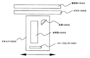
イメージセンサ素子としては、CCD型や単結晶CMOS型のセンサが多く使用されている。これらの素子を用いて、密着型光学系を採用したときのスキャナの断面図を図40に示す。CCD型(CMOS型)のイメージセンサ10001の上には、ロッドレンズアレイなどの光学系10002が配置されている。これは、原稿(被写体)上の画像がイメージセンサ10001上に映し出されるようにするために用いられる。像の関係は、等倍系である。光源10003は、被写体10004に光を照射できるような位置に配置されている。用いられる光源としては、LEDや蛍光灯などが多く用いられる。そして、最上部にガラス10005が配置され、ガラス10005の上に被写体10004が配置される。なお図4に示すスキャナの動作については以下の通りである。まず、光源10003を出た光は、ガラス10005を通って原稿に入射する。そしてその光は被写体10004で反射され、ガラス10005を通って、光学系10002に入射する。光学系10002に入射した光は、次いで、イメージセンサ10001に入射し、そこで光電変換される。そして、電気に変換された信号は、外部に読み出される。そしてイメージセンサ10001で一列分の信号を読み取ったら、スキャナ10006を移動して、再び同様の動作を繰り返す。
【0008】
なお図4に示すスキャナは、ラインセンサであるが、該ラインセンサで2次元の被写体を読み取る場合には、センサ、あるいは、被写体のどちらか一方を動かす必要がある。そのため装置が大きくなったり、読み取り速度が遅くなったり、機械的強度が弱くなったりしてしまう。そこで、画素を2次元に配列した密着型のエリアセンサが研究されている。被写体に光を当てるために、基板は光を通す必要がある。そのため基板は、透明なものであることが必要であり、例えば、ガラスのように透明であることが必要になる。エリアセンサでは、画素が2次元に配列されているため、読み取り時に動かす必要がない。このような密着型エリアセンサは、テレビジョン学会技術報告:1993.3.4:p25:アモルファスシリコン2次元イメージセンサとその応用、Jpn.J.Appli.Phys.Vol.32(1993) pp458-461:Two-Dimensional Contact-Type Image Sensor Using Amorphous Silicon
Photo-Transistorなどに発表されている。
【0009】
次いで、イメージセンサ素子を用いて、被写体をカラーで読み取る場合について述べる。カラーの画像を読み込みたい場合は、特別な手法(方式)を用いる必要がある。その手法(方式)としては、大きく分けて、(a)光源切り替え方式、(b)フィルタ切り替え方式、(c)カラーイメージセンサを使う方式の3つがある。(a)光源切り替え方式は、3色の光源(蛍光灯、LEDなど)を順次点滅し、モノクロイメージセンサで原稿の画像情報を順次読み取り、赤、緑、青の信号出力を得るというものである。(b)フィルタ切り替え方式は、白色光源とモノクロイメージセンサの間に赤、緑、青のカラーフィルタを設けて、該フィルタを切り替えて、順次読み取りを行い、赤、緑、青の信号出力を得るというものである。(c)カラーイメージセンサ方式は3ラインのイメージセンサとカラーフィルタを1パッケージに組み込んだカラーイメージセンサであり、色分解と読み取りを同時に行うというものである。
【0010】
次いで、光電変換などを行うセンサ部について述べる。通常は、センサ部にPN型のフォトダイオードが設けられて、該フォトダイオードを用いて、光を電気に変換する。より詳しくは、被写体の情報を画像信号に変換する。その他には、PIN型のダイオード、アバランシェ型ダイオード、npn埋め込み型ダイオード、ショットキー型ダイオード、フォトトランジスタなどがある。その他には、X線用にフォトコンダクタや、赤外線用のセンサなどもある。これらの光電変換素子については、固体撮像素子の基礎ー電子の目のしくみ:安藤隆男、菰淵寛仁著:日本理工出版界に述べられている。
【0011】
【発明が解決しようとする課題】
本発明は、イメージセンサ機能を有するエリアセンサに関するもので、より詳細にはEL素子を光源として利用し、マトリクス状に配置されたフォトダイオードと複数の薄膜トランジスタ(TFT)とによって構成されるエリアセンサおよびエリアセンサを備えた表示装置に関するものである。本発明で用いる表示装置(エリアセンサ)は、画像表示機能と画像読み取り機能を一体化したものであり、各画素には、EL発光部(EL発光素子、RGBの合計3個)とイメージセンサ素子(1個)がある。イメージセンサ機能とは、画面に被写体を密着させて、センシングを行い、被写体の情報を読み取る機能である。この場合には、EL素子をイメージセンサ用の照明として用いる。つまり、始めに画素にマトリクス状に設けられたEL素子を発光させ、EL素子から発せられた光を被写体に照射させる。そして、その反射した光がフォトダイオードに照射されることによって、被写体の情報を読み取る仕組みになっている。なおカラーの被写体の場合には、3回センシングを行って画像の情報を読み取る。また本発明で用いる表示装置は、EL発光部を発光させて、画像を表示する表示機能を有しており、表示機能を機能させる場合には、イメージセンサ機能は停止している。
【0012】
ここで、光の屈折について説明する。光の屈折は、図25に示すように入射光の角度(入射角)とその媒質の屈折率により決まる。さらに、この関係は以下の数1(式(1)、スネルの法則)に従う。屈折率がn1である媒質801においてθ1の角度で入射した光(入射光)が、屈折率がn2である媒質802に出射するとき、以下の数1(式(1))を満たすような角度θ2の光(屈折光)となる。
【0013】
【数1】
n1*sinθ1=n2*sinθ2・・・(1)
【0014】
屈折光または透過光の角度θ2が90°となるような入射角θ1を臨界角とよぶ。また、媒質802に対する入射角θ1が臨界角よりも大きくなるときに、入射光は全反射する。つまり、光が媒質801に閉じ込められることになる。
【0015】
さらに、エネルギーの反射率(R)及び透過率(T)は、以下に示す数2、数3(式(2)、式(3)、フレネルの法則)が成り立つ。
【0016】
【数2】

【数3】
T=1−R
【0018】
ここで、EL素子とイメージセンサ素子を一画素とし、該画素をマトリクス状に基板上(一例としてここではガラス基板とする)に設けた表示装置(エリアセンサ)における被写体とセンサ部との関係について述べる。
【0019】
まず、画素102がマトリクス状に設けられたガラス基板803と被写体804とが完全に密着している場合について説明する(図26)。完全に密着している場合とは、ガラス基板803と被写体804との間に完全に空気が無い状態のことである。図26において、矢印は光の進行方向を表しており、また画素102、EL素子部103およびフォトダイオード部104は図2に示すものを概略化したものであるので説明は省略する。また画素102は、マトリクス状に設けられているが、図26ではその一部を表している。図27、図28においても同様である。
【0020】
EL素子部103から発せられた光は、被写体804に向けてあらゆる方向に拡散して、被写体804に照射される。画素102は、ガラス基板803上にマトリクス状に設けられており、EL素子部103から発せられる光は被写体804にほぼ均一に照射される。よって、EL素子部103から発せられた光は、被写体804の反射率に応じて反射される。そしてガラス基板803を介して、フォトダイオード部104に照射される光は、すべて被写体804からの反射光となる。
【0021】
つまり、被写体804とセンサ部(フォトダイオード部104)が完全に密着している場合(図26)においては、EL素子部103から発せられた光は、被写体804に反射し、その反射光がフォトダイオード部104に照射されることにより、被写体804の情報をよみとるという仕組みになっている。すなわち、EL素子部103から発せられた光は、ガラス基板803を通って、被写体804に照射され、また、フォトダイオード部104に照射される光はすべて被写体804からの反射光であることが分かる。
【0022】
次に、ガラス基板803と被写体804の間の一部に空気805が存在する場合について説明する(図27)。EL素子部103から発せられた光はあらゆる方向に拡散して照射される。このとき、EL素子部103から発せられた光が、ガラス基板803に入射して空気805との界面に到達したとき、屈折して屈折光として被写体804に照射する場合と、反射して反射光としてフォトダイオード部104に照射する場合がある。本明細書中では、EL素子部103から発せられた光が、ガラス基板803と空気805との界面において、全反射してしまう光、すなわちガラス基板803に閉じこめられてしまう光をノイズ光とよぶ。本来ならば、EL素子部103から発せられた光は被写体804に照射され、そして被写体804において反射し、反射光としてフォトダイオード部104に照射されるべきである。しかし、EL素子部103から発せられ、基板803と空気805の界面において全反射した光(ノイズ光)は、被写体804に照射されることなく、そのままフォトダイオード部104に照射されてしまう。このようなノイズ光は被写体804の情報をぼやけて読み取る原因となる。
【0023】
ここで、光の屈折の関係をスネルの法則(数1、式(1))を参考にして考える。ここでは、一例として基板をガラス基板としているので、ガラス基板の屈折率(n=1.52)と、空気の屈折率(n=1.0)を参考にする。また、ノイズ光を発生させないためには、θ4=90°であればよいので、これらの値をスネルの法則(数1、式(1))に代入する。そうすると、数4(式(4))のような値が算出される。
【0024】
【数4】
θ3=41.1・・・(4)
【0025】
すなわち、ガラス基板803と被写体804との間に空気805が存在する場合には、EL素子部103から発せられた光がガラス基板803と空気805との界面に到達したときに、その入射角が41.1°以上の場合に全反射するということである。また、図39および数4(式(4))を参考にすると入射角が35°以上41.1°以下の場合において反射率が上昇しており、EL素子部103から発せられた光が、ガラス基板803と空気805との界面において、反射する光が急増する。すなわち、入射角が35°以上41.1°以下の場合においては、EL素子部103から発せられた光が、ガラス基板803と空気805との界面において、すべて反射する場合と、屈折する場合とが存在する。また図39より、EL素子部103から発せられた光が、ガラス基板803と空気805との界面において、入射角が35°以下の場合においては、ほとんど反射せず、屈折して光が外に出ることが分かる。
【0026】
次にガラス基板803と被写体804とが完全に離れている場合について説明する(図28)。この場合は、ガラス基板803と被写体804との間に完全に空気805が存在する場合である。EL素子部103から発せられた光は、被写体807に向けてあらゆる方向に拡散して、被写体804に照射される。そしてEL素子部103から発せられた光は、ガラス基板803と空気805との界面に到達したときに、入射角に応じて、反射光か、屈折光かのどちらかとなる。
【0027】
上述のように、図39および数4(式(4))を参考にすると、EL素子部103から発せられた光は、入射角が41.1°以上の場合は全反射し、入射角が35°以上41.1°未満の場合は反射する光と、屈折する光とに分類される。入射角が35°以下の場合はほとんどの光が、屈折光として被写体に照射されるが、図39に示すように、反射する光も少し存在する。もちろん、全反射する光はノイズ光としてフォトダイオード部104に照射されるが、EL素子部103から発せられる光は、あらゆる方向に拡散して照射され、かつ、EL素子部103から発せられる光は、ある角度以上の入射角のみが全反射するため、フォトダイオード部104には均一にノイズ光が照射されるということが分かる。
【0028】
また、EL素子部103から発せられた光が、ガラス基板803と空気805との界面で屈折光としてガラス基板803の外に出た場合は、被写体804に照射される。そして被写体804の反射率に応じて光が反射され、その反射光がフォトダイオード部104に照射される。すなわちこの場合においては、フォトダイオード部104に照射される光は、被写体804で反射した反射光と、それぞれのフォトダイオード部104に均一に照射されるノイズ光となる。
【0029】
上述したように、ガラス基板803と被写体804との間の一部に空気805がある場合(図27)、またガラス基板803と被写体804との間が完全に離れている場合(図28)は、ガラス基板803と空気805との界面において全反射する光がノイズ光として存在する。ノイズ光は被写体804の情報をぼやけてよみとってしまう原因となっている。本発明では、ガラス基板803と被写体804とが完全に密着している場合、ガラス基板803と被写体804との間の一部に空気805が存在する場合、ガラス基板803と被写体804とが完全に離れている場合のいずれにおいても、被写体804の情報が正確によみとれるようにすることを課題とする。また被写体804に凹凸があっても、被写体804の情報を正確に読み取れるようにすることを可能とする。
【0030】
【課題を解決するための手段】
本発明では、EL素子部103と被写体804との間に、ガラスファイバプレート、または光ファイバプレートを設け、ノイズ光を光吸収層により吸収させることによって、上記課題を解決する。
【0031】
本発明では、それぞれ光吸収層で覆った複数のガラスファイバを軸が平行になるように束ねる。なお本明細書で用いられるガラスファイバとは、細い線状のガラス線、またはガラス棒とよばれるものを使用する。このような複数のガラスファイバを束ね、その軸と垂直方向にプレート状にスライスする。そのスライスしたものを、本明細書中ではガラスファイバプレートとよぶ(図29)。なお図29では、ガラスファイバ821の断面は円状となっているが、本発明ではこれに限らず、断面は楕円状でもよいし、多角形状でもよいが、図30に示すように、軸と平行方向の断面が四角形であることが望ましい。
【0032】
また、それぞれ光吸収層で覆った複数のガラスファイバを用いたガラスファイバプレート以外に、複数のガラスファイバを軸が平行になるように束ね、その軸を垂直方向にプレート状にスライスしたものを用いてもよい。この場合には、ガラスファイバとガラスファイバの間に光吸収層を設ける。
【0033】
そして本発明では、このようなガラスファイバプレートをセンサ部と被写体の間に設ける。図30は、EL素子部103およびフォトダイオード部104を有する画素102が、マトリクス状に一つの基板上に設けられた一部を示しており、EL素子部103から光吸収層822で覆われた複数のガラスファイバ821に光が照射される様子を表した図である。図30において、画素102、EL素子部103およびフォトダイオード部104は図2に示すものと同じであるので説明は省略する。θ7、θ8およびθ9はガラスファイバ821と空気825との界面においての入射角を示しており、θmax1はガラスファイバ821と空気825との界面においての臨界角を示している。また矢印は光の進行方向を示している。
【0034】
図30から、EL素子部103から発せられた光の進行方向が光吸収層822の場合は、光が吸収されていることが分かる。それ以外の光は、ガラスファイバ821と空気825との界面において、入射角がθ10(ただしθ10<θmax1)の場合は、屈折して屈折光826として出射する。ガラスファイバ821と空気825との界面において、入射角がθ9(ただしθ9<θmax1)の場合はガラスファイバ821と空気825の界面で全反射し、反射光827として再び光吸収層822に吸収される。もしくは、ガラスファイバ821と空気825との界面において、入射角がθ8(ただしθ8<θmax1)場合は、ガラスファイバ821と空気825の界面で全反射し、反射光828としてフォトダイオード部104に照射される。
【0035】
ここで、EL素子部103から発せられた光が、ガラスファイバ821と空気825の界面において反射され、その反射光828がフォトダイオード部104に照射されないようにしたい。なぜなら、反射光828のような光がフォトダイオード部104に照射されることが、被写体824の情報を正確に読み取ることが出来ない原因であるからである。
【0036】
つまり、被写体824がガラスファイバ821に完全に密着している場合、被写体824とガラスファイバ821との間の一部に空気825が存在する場合、被写体824とガラスファイバ821とが完全に離れている場合のいずれの場合にも被写体824の情報を完全に読み取ることができるようにしたい。すなわち、ガラスファイバ821と空気825との界面で全反射し、その反射光がフォトダイオード部104に照射されないようにすればよい。この場合、そのための条件式を、1本のガラスファイバ821の長さ(B)と断面の直径(A)とガラスの屈折率から算出できる。
【0037】
さらに、EL素子部103から発せられた光が、ガラスファイバ821と空気825の界面で全反射しないようにしたい。また全反射したとしても、その反射光が、光吸収層822に吸収されればよい。以上の状況をふまえると、ガラスファイバ821の断面の直径(A)の半分と、ガラスファイバ821の長さ(B)から以下の式(5)を導き出せる。
【0038】
【数5】
tanθmax1=A/2B・・・(5)
【0039】
ガラスファイバ821の断面の直径(A)の半分と、ガラスファイバ821の長さ(B)が、式(5)を満たせば、EL素子部103から発せられた光が、ガラスファイバ821と空気825の界面で全反射され、フォトダイオード部104に照射される光はない。よって、一本のガラスファイバ821の断面の直径(A)と長さ(B)との関係式は式(6)のように表すことができる。
【0040】
【数6】
θmax>tan-1(A/2B)・・・(6)
【0041】
上述のように、本発明ではガラスファイバ821の断面の直径(A)と長さ(B)との関係が式(6)を満たすようなガラスファイバ821を用いることが好ましい。このようにすることによって、被写体とセンサ部が完全に密着している場合、被写体とセンサ部の間の一部に空気が存在する場合、被写体とセンサ部が完全に離れている場合のいずれの場合にも被写体の情報をぼやけることなく読み取ることができる。
【0042】
また、ガラスファイバプレート820の代わりに、光ファイバプレート830を被写体とセンサ部の間に設けてもよい。図31にあるように、本明細書中では、複数本の光ファイバ831をそれらの軸が平行になるように束ねて、それぞれの光ファイバ831の軸と垂直方向にプレート状にスライスしたものを光ファイバプレート830とよぶ。1本の光ファイバ831は、光吸収層834と光透過層835とからなっており、光透過層835は光吸収層834に覆われている。光透過層835は、屈折率の高いコア部832と、その周辺を囲むコア部832よりも屈折率の低いクラッド部833からなっている。このような構造をもつ光ファイバプレートは、既に市販されており、浜松ホトニクス社のファイバオプティクプレート(FOP)、旭硝子社のファイバアレイプレート(FAP)、ワイオーシステム社の光ファイバプレート等がある。
【0043】
ここで、EL素子部103から発せられた光が、光ファイバ831のコア部832とクラッド部833との境界面を全反射しながら伝搬していくための条件を考えてみる。
【0044】
図33を参照する。図33のEL素子部103は、図2に示すものと同じである。またコア部832、クラッド部833、光吸収層834および光透過層835は、図32に示すものを同じであるので、ここでは説明は省略する。そして、コア部832の屈折率をn10、クラッド部833の屈折率をn11とし、θa、θb、θcおよびθdは角度を示す。
【0045】
まず、EL素子部103から発せられた光が、光ファイバ831と空気825との界面で全反射しないための条件を考える。全反射させないためには、θb=90°であればよい。これをスネルの法則(数1、式(1))に代入する。そうすると以下の式(7)が求められる。
【0046】
【数7】
n10*sinθa=1・・・(7)
【0047】
ここで、EL素子部103から発せられた光が、光ファイバ831と空気825との界面で全反射しないためには、左辺よりも右辺の方が大きければよい。よって、数8(式(8))を満たせばよい。
【0048】
【数8】
n10*sinθa<1・・・(8)
【0049】
またEL素子部103から発せられた光が、EL素子部103と光ファイバ831との界面においての入射角がEL素子部103と光ファイバ831との界面においての臨界角よりも大きい場合には、EL素子部103から発せられた光はコア部832とクラッド部833との界面で全反射しない。このような光は、光吸収層834に吸収させればよい。よって、下記の関係式(9)が求められる。まずはスネルの法則(数1、式(1))に当てはめる。
【0050】
【数9】
n10*sinθc=n11*sinθd・・・(9)
【0051】
このとき、θd=90、θc=90−θaとなり、これを数7(式(7))、数8(式(8))および数9(式(9))に代入する。そうすると以下の式(10)が求められる。
【0052】
【数10】
n10*sinθc=n10*sin(90−θa)=n11・・・(10)
【0053】
このとき、EL素子部103から発せられた光は、光ファイバのコア部832とクラッド部833の境界面において、反射させずに、コア部832からクラッド部833に入射することにより、光吸収層834に吸収させればよい。よって、右辺よりも左辺の方が大きければよく、以下の数11(式(11))を満たせばよい。
【0054】
【数11】
n10*sin(90−θa)=n10*cosθa>n11・・・(11)
【0055】
ここで、開口数(N.A.)を考えると、開口数(N.A.)は以下の式(12)で表すことができる。
【0056】
【数12】
N.A.=(n10 2−n11 2)1/2・・・(12)
【0057】
ここで、本発明のエリアセンサ(表示装置)には、数7(式(7))、数10(式(10))を満たす光ファイバを用いればよいので、数7(式(7))、数10(式(10))を数11(式(11))に代入する。そうすると、以下の数13(式(13))が求められる。
【0058】
【数13】
N.A.=(n10 2−n11 2)1/2<n10*sinθa<1・・・(13)
【0059】
上記のように、N.A.(開口数)は1未満であることが望ましい。より最適なN.A.(開口数)を求めたい場合には、θa、θb、θcおよびθdに数値を代入して求めるとよい。N.A.(開口数)は、光ファイバ831のコア部832とクラッド部833の屈折率により求めることができる。
【0060】
図32において、EL素子部103から発せられた光が、EL素子部103と光ファイバ831のコア部832との境界面において、臨界角(θmax2)以上の角度で光ファイバ831に入射した場合、すなわち、入射角がθ14(ただしθ14>θmax2)の場合には、光ファイバ831のコア部832とクラッド部833との境界面において全反射せずに、迷光として複数本の光ファイバ831を横断して伝搬しようとする。しかし本発明で用いる光ファイバ831は、光吸収層834で覆われているために吸収される。ここで、θmax2とは、EL素子部103から発せられた光が、光ファイバ831のコア部832に入射するときの臨界角を示す。
【0061】
また、EL素子部103から発せられた光が、臨界角(θmax2)以下の角度で光ファイバ831に入射した場合は、コア部832とクラッド部833との境界面における全反射により、光は伝搬していく。伝搬した光が、光ファイバ831と空気825との界面に到達した場合、その界面において臨界角(θmax3)よりも小さい場合は、屈折光836として、被写体824に照射される。ここで、θmax3とは、EL素子部103から発せられた光が、光ファイバ831を通って、光ファイバ831のコア部832と空気825との界面に入射する場合の臨界角を示す。
【0062】
EL素子部103から発せられた光が、光ファイバ831のコア部832とクラッド部833の境界面における全反射により、光は伝搬していく。伝搬した光が、光ファイバ831と空気836との界面に到達した場合、その界面において入射角(θ12)が臨界角(θmax3)よりも小さい場合がある。すなわち、EL素子部103から発せられた光が、光ファイバ831と空気825との界面においての入射角がθ12(ただしθ12>θmax3)の場合は、光ファイバ831と空気825との界面において全反射する。全反射した光は、反射光837として、コア部832とクラッド部833との境界面の全反射を繰り返すことにより、反射光837は伝搬してフォトダイオード部104に照射される。
【0063】
光ファイバ831と空気825との界面に到達した光は、入射角により、屈折光836として光ファイバ831の外に出て、被写体824に照射される場合と、反射光837のように再び光ファイバ831内を伝搬してフォトダイオード部104に照射される場合とがある。反射光837のような光が、フォトダイオード部104に照射されることは、被写体の光を正確によみとることが出来ない原因となる。そこで、光ファイバプレートを用いる場合には、入射角を調節する必要があり、また入射角は開口数(N.A.)、すなわちコア部832の屈折率に依存する。
【0064】
ガラス基板803と被写体804との間の一部に空気805がある場合、ガラス基板803と被写体804との間が完全に離れている場合は、ガラス基板803と空気805との界面で全反射する光がノイズ光として存在する。ノイズ光は被写体の情報をぼやけてよみとってしまう原因となっている。そこで本発明は被写体とセンサ部との間にガラスファイバプレート、または光ファイバプレートを設けることにより、ノイズ光を光吸収層に吸収する。すなわち、ガラスファイバ、または光ファイバと空気との界面で全反射する光を、光吸収層に吸収する。よって、EL素子から発せられた光が被写体で反射して、その反射光がフォトダイオードに照射されるために、被写体の情報を正確に認識することができる。
【0065】
すなわち本発明では、ガラス基板803と被写体804とが完全に密着している場合、ガラス基板803と被写体804との間の一部に空気が存在する場合、ガラス基板803と被写体804とが完全に離れている場合の、いずれの場合においても被写体804の情報を正確に読み取ることができるエリアセンサを提供する。また該エリアセンサを備えた表示装置を提供する。
【0066】
【発明の実施の形態】
(実施の形態1)
本発明のエリアセンサ(表示装置)には、図29にあるようなガラスファイバプレート820、または図31にあるような光ファイバプレート830が被写体とセンサ部との間に設けられる。本実施の形態では、EL素子部103に設けられたEL素子が下面出射するエリアセンサ(表示装置)について、図34を用いて説明する。本明細書中で下面出射するとは、TFTを設けている基板上において、TFTを設けている側とは反対側にEL素子部から発せられた光が照射されることを示す。そしてファイバプレート860の下部に被写体を設けるようにする。なお図34において、画素102、EL素子部103およびフォトダイオード部104は図2と同じであるので、説明は省略する。また本明細書中では、基板上にマトリクス状に設けられている複数の画素をセンサ部とよぶが、図34ではその一部を示す。なお図35〜38においても同様である。またファイバプレート860とは、ガラスファイバプレート820もしくは光ファイバプレート830のどちらかを示す。
【0067】
本実施の形態では、EL素子が下面出射するためにファイバプレート860(ガラスファイバプレート820または光ファイバプレート830)をセンサ部が形成される基板として用いる。
【0068】
ファイバプレート860はセンサ部が形成される基板として用いられ、ファイバプレート860をセンサ部と被写体804との間に設ける。上述したように、EL素子部103から発せられた光がファイバプレート860を透過し、ファイバプレート860と空気との界面で全反射する光は光吸収層に吸収される。本実施の形態では、被写体とファイバプレート860が完全に密着している場合、また被写体とファイバプレート860との間の一部に空気が存在する場合、また被写体とファイバプレート860とが完全に離れている場合のいずれの場合においても、被写体の情報を正確によみとることができる。すなわち、被写体とファイバプレート860が完全に密着している場合では、フォトダイオード部104に照射される光は被写体からの反射光のみであり、また被写体とファイバプレート860との間の一部に空気が存在する場合、また被写体とファイバプレート860とが完全に離れている場合は、フォトダイオード部104に照射される光は被写体からの反射光とそれぞれのフォトダイオードに均一に照射されるノイズ光となる。すなわち、いずれの場合にも被写体の情報を正確に読み取ることができる。
【0069】
(実施の形態2)
本実施の形態では、実施の形態1とは異なる例について、図35を用いて説明する。本発明のエリアセンサ(表示装置)には、図29にあるようなガラスファイバプレート820、または図31にあるような光ファイバプレート830が被写体とセンサ部との間に設けられる。本実施の形態では、EL素子部103に設けられたEL素子が上面出射するエリアセンサ(表示装置)について、図35を用いて説明する。本明細書中で上面出射するとは、TFTを設けている基板上において、TFTを設けている側にEL素子部から発せられた光が照射されることを示す。また被写体を読み取る際には、ファイバプレート870の上部に被写体を設けるようにする。
【0070】
本実施の形態では、EL素子部103が上面出射するために、図29にあるようなガラスファイバプレート820、または図31にあるような光ファイバプレート830をセンサ部が形成される基板として用いることは出来ない。そのため本実施の形態で用いる基板871には、可撓性のプラスチックフィルム、ガラス基板、石英基板、プラスチック基板、シリコン基板もしくはセラミックス基板などの基板を用いるとよい。
【0071】
本実施の形態では、センサ部を形成した基板871上に絶縁膜などの保護膜を必要に応じて形成し、その上にファイバプレート870を設ける。
【0072】
以上のようにして、ファイバプレート860をセンサ部と被写体との間に設ける。上述したように、EL素子部103から発せられた光が、ファイバプレート860を透過し、ファイバプレート860と空気との界面で全反射する光は光吸収層に吸収される。本実施の形態では、被写体とファイバプレート860が完全に密着している場合、また被写体とファイバプレート860との間の一部に空気が存在する場合、また被写体とファイバプレート860とが完全に離れている場合のいずれの場合においても、被写体の情報を正確によみとることができる。すなわち、被写体とファイバプレート860が完全に密着している場合では、フォトダイオードに照射される光は被写体からの反射光のみであり、また被写体とファイバプレート860との間の一部に空気が存在する場合、また被写体とファイバプレート860とが完全に離れている場合は、フォトダイオードに照射される光は被写体からの反射光とそれぞれのフォトダイオードに均一に照射されるノイズ光となる。よって、いずれの場合にも被写体の情報を正確に読み取ることができる。
【0073】
なお、本実施の形態は実施の形態1と自由に組み合わせることが可能である。
【0074】
(実施の形態3)
本実施の形態では、可撓性のプラスチックフィルム、ガラス基板、石英基板、プラスチック基板、シリコン基板もしくはセラミックス基板などの基板に、ガラスファイバプレート、または光ファイバプレートを光学のり等により接着したものを用いた表示装置(エリアセンサ)について図36を用いて説明する。光学のり等で接着する場合には、空気が入らないように注意する。なお用いられる光学のりは、用いる基板とガラスファイバプレートおよび光ファイバプレートとの界面で反射することを避けるために、ガラスファイバの光透過層、光ファイバのコア部および基板と屈折率が同じであることが望ましい。
【0075】
本実施の形態では、EL素子部103に設けられたEL素子が下面出射するエリアセンサ(表示装置)について示す。基板840は、可撓性のプラスチックフィルム、ガラス基板、石英基板、プラスチック基板、シリコン基板もしくはセラミックス基板などのうちいずれかが用いられる。ファイバプレート841にはガラスファイバプレートもしくは光ファイバプレートのどちらかが用いられる。そして基板840とファイバプレート841を光学のり等により接着したものを、被写体とセンサ部との間に設ける。
【0076】
EL素子部103が下面出射する場合には、まず基板840上にセンサ部を形成し、その後、ファイバプレート841を接着してもよい。また、最初に基板840とファイバプレート841を接着しておき、その上にセンサ部を形成してもよい。このような作製工程は設計者が自由に設計することが出来る。
【0077】
EL素子部103から発せられた光は、あらゆる方向に拡散する。基板840とファイバプレート841の屈折率が異なる場合は、基板840とファイバプレート841との界面において、入射角によっては反射する光が生じる。このような反射光は、フォトダイオードに照射され、被写体の情報をぼやけて認識してしまう大きな原因となる。よって、基板840とファイバプレート841の屈折率は同じであることが望ましい。より詳細には、基板840とガラスファイバの光透過層、基板840と光ファイバのコア部との屈折率は同じあることが望ましい。また上述したように、基板840とファイバプレート840を接着する光学のりも屈折率は同じであることが望ましい。
【0078】
EL素子部103から発せられた光は、あらゆる方向に拡散して照射されるが、基板840とファイバプレート841との界面で反射する光以外は、EL素子部103から発せられた光は、ファイバプレート841に入射される。ファイバプレート841とは、ガラスファイバプレートか光ファイバプレートのどちらか一つを示す。なおガラスファイバプレートまたは光ファイバプレートに光が入射した場合については上述してあるので、本実施の形態では説明は省略する。
【0079】
なお被写体804とフォトダイオード部104の距離は、なるべく短い方が好ましい。そのため、本実施の形態で用いる基板840は、ファイバプレート841と接着するので、通常用いられる基板840よりも薄い方が好ましい。なおファイバプレート841の厚さは、ガラス基板の厚さよりも、厚くても構わない。例えばガラス基板を用いるときには、通常用いられるガラス基板(7mm厚)よりも、比較的うすいガラス基板(5mm厚)を用いてもよい。また通常用いられるガラス基板(7mm厚)を研磨して、厚さを薄くして用いてもよい。
【0080】
なお、本実施の形態は実施の形態1〜2と自由に組み合わせることが可能である。
【0081】
(実施の形態4)
本実施の形態では、基板850とファイバプレート851の間に吸収材によるスペーサ(図示せず)を設けた例について、図37を用いて説明する。なお図37には、EL素子部103に設けられたEL素子が下面出射するエリアセンサ(表示装置)を示す。基板850とファイバプレート851との間にスペーサ等を設ける場合には、基板850上に、均一に、且つ、等しい間隔ごとに設ける。ファイバプレート851とはガラスファイバプレートもしくは光ファイバプレートのどちらかを示す。また本実施の形態では、基板850とファイバプレート851の間に吸収材を設けたが、基板の外枠のみに基板850とファイバプレート851とを固定するスペーサ等を用いてもよい。スペーサが用いられる箇所は設計者が自由に設計することが出来る。基板850とファイバプレート851との間に用いるスペーサは、EL素子部103から発せられた光が、基板850およびファイバプレート851との界面で全反射することを防ぐために、基板850およびファイバプレート851(より詳細には、ガラスファイバの光透過層および光ファイバのコア部を示す)と屈折率が同じであることが望ましい。また基板の外枠に用いるスペーサの屈折率は、特に限定されず、任意のもので構わない。なお図37では被写体804とファイバプレート851とが完全に離れている場合を示す。
【0082】
EL素子部103から発せられる光はあらゆる方向に拡散して照射される。図37に示すエリアセンサ(表示装置)においては、基板850とファイバプレート851との界面に空気852が存在するために、入射角の違いに応じて、基板850と空気852との界面において全反射する光と、屈折して屈折光としてファイバプレート851に入射する場合とがある。図37においては、一例として屈折光及び全反射した光とを示し、基板850と空気852との界面において、入射角がθ16(ただしθ16<θmax)の場合は屈折して屈折光として出射しており、入射角がθ17(ただしθ17>θmax)の場合は、全反射してノイズ光としてフォトダイオードに照射されている。
【0083】
EL素子部103から発せられた光は、被写体804に向けてあらゆる方向に拡散して照射される。EL素子部103から発せられた光は、基板850と空気852との界面に到達した場合、図36にあるように、入射角に応じて、反射光か屈折光かのどちらかとなる。
【0084】
ここで、基板850をガラス基板とする。ガラス基板には、様々な屈折率のものが存在するが、本実施の形態では一例として、n=1.52とする。数4(式(4))および図39を参考にすると、EL素子部103から発せられた光は、入射角が41.1°以上の場合は全反射し、入射角が35°以上41.1°未満の場合は反射する光と屈折する光とが存在し、入射角が35°以下の場合は、多くの場合は屈折光として被写体804に照射される。もちろん、全反射する光はノイズ光としてフォトダイオード部104に照射されるが、EL素子部103から発せられる光は、あらゆる方向に拡散して照射され、かつ、基板850と空気852との界面において、図39を参照すると、それぞれの入射角の反射率に応じて、EL素子部103から発せられた光は、全反射するため、フォトダイオード部104には均一にノイズ光が照射されるということが分かる。
【0085】
またEL素子部103から発せられた光が、基板850と空気852との界面で屈折光として基板850の外に出た場合は、ファイバプレート851に照射される。なおファイバプレート851とは、ガラスファイバプレートか光ファイバプレートのどちらかを示す。ガラスファイバプレートまたは光ファイバプレートに、光が入射した場合については、上述してあるため本実施の形態では説明は省略する。
【0086】
ファイバプレート851を透過した光は、被写体804の反射率に応じて光が反射され、その反射光がフォトダイオード部104に照射される。すなわち本実施の形態においては、フォトダイオード部に照射される光は、被写体で反射した反射光と、それぞれのフォトダイオード部に均一に照射されるノイズ光となる。
【0087】
また本実施の形態のように、それぞれのフォトダイオードに均一に照射されるノイズ光の存在があらかじめ分かっている場合には、被写体の情報をより正確に読み取れるように、事前に均一に照射されるノイズ光を測定しておき、その測定した値をもとに被写体の情報を読み取ったときに信号を補正すればよい。このようにすると、ガラス基板803と被写体804とが完全に密着している場合、ガラス基板803と被写体804との間の一部に空気が存在する場合、ガラス基板803と被写体804とが完全に離れている場合の、いずれの場合においても被写体804の情報が正確によみとれる。
【0088】
本実施の形態では、基板850とファイバプレート851とをスペーサ等により接着して用いるため、フォトダイオード部104と被写体804との距離が長くなってしまう。EL素子部103から発せられた光は、被写体804において反射し、その反射光は、被写体804の反射したところの直上のフォトダイオード部104に照射されるべきである。しかし、フォトダイオード部104と被写体804との距離が長い場合には、被写体804からの反射光が、本来照射されるべきではないフォトダイオード部104に光が照射される可能性が高くなる。このような光は、被写体804の情報をぼやけてよみとる原因となる。しかしこの場合には、ファイバプレート851の厚さを薄くする必要はなく、基板850の厚さをなるべく薄くする。また同様に、スペーサの厚さを調節することによって空気852の厚さをなるべく薄くする。
【0089】
なお、本実施の形態は実施の形態1〜3と自由に組み合わせることが可能である。
【0090】
(実施の形態5)
本実施の形態では、基板880とファイバプレート881の間に吸収材によるスペーサ(図示せず)を設けた例について、図38を用いて説明する。なお図38には、EL素子部103に設けられたEL素子が上面出射するエリアセンサ(表示装置)を示す。なお、基板880とファイバプレート881との間にスペーサ等を設ける場合には、基板880上に、均一に等しい間隔ごとに設ける。ファイバプレート881とはガラスファイバプレートもしくは光ファイバプレートのどちらかを示す。また、本実施の形態では、基板の外枠に基板880とファイバプレート881とを固定するスペーサ等を用いてもよい。なお、基板880とファイバプレート881との間に用いるスペーサはEL素子部103から発せられた光が、基板850およびファイバプレート851との界面で全反射することを防ぐために、基板880およびファイバプレート881(ガラスファイバの光透過層および光ファイバのコア部を指す。)と屈折率が同じであることが望ましい。また、基板の外枠に用いるスペーサの屈折率は任意で構わない。なお、図38では被写体804とファイバプレート881とが完全に離れている場合を示す。
【0091】
本実施の形態では、センサ部を形成した基板880上に絶縁膜などの保護膜を形成し、その上にスペーサ等でファイバプレート881を設ける。本実施の形態では、EL素子部103から発せられる光が上面出射するために、被写体804とセンサ部の間にファイバプレート881を設けるためには、ガラスファイバプレートまたは光ファイバプレートをセンサ部が形成される基板として用いることが出来ない。そのため、本実施の形態で用いる基板880には、可撓性のプラスチックフィルム、ガラス基板、石英基板、プラスチック基板、シリコン基板もしくはセラミックス基板などの基板を用いればよい。
【0092】
本実施の形態では、センサ部を形成した基板880上に絶縁膜などの保護膜を形成し、その保護膜とファイバプレート881とをスペーサ等により接着して用いるため、フォトダイオード部104と被写体804との距離が長くなってしまう。EL素子部103から発せられた光は、被写体804において反射し、その反射光は、被写体804の反射したところの直上のフォトダイオード部104に照射されるべきである。しかしフォトダイオード部104と被写体804との距離が長い場合には、被写体804からの反射光が、本来照射されるべきではないフォトダイオード部104に光が照射される可能性が高くなる。このような光は、被写体804の情報をぼやけてよみとる原因となる。しかし、この場合は、ファイバプレート881の厚さを薄くする必要はなく、基板880の厚さをなるべく薄くする。また同様に、スペーサの厚さを調節することによって空気852の厚さをなるべく薄くする。
【0093】
なお、本実施の形態は実施の形態1〜4と自由に組み合わせることが可能である。
【0094】
【実施例】
以下に、本発明の実施例について説明する。
【0095】
(実施例1)
以下に、本発明のエリアセンサ(表示装置)の構成を詳しく説明する。本発明のエリアセンサ(表示装置)は被写体の情報の読み取り、および画像の表示を行うセンサ部と、センサ部の駆動を制御する駆動部とを有している。図1に本発明のセンサ部の回路図を示す。
【0096】
センサ部101はソース信号線S1〜Sx、電源供給線V1〜Vx、ゲート信号線G1〜Gy、リセット信号線RG1〜RGy、選択信号線SG1〜SGy、センサ用信号出力線SS1〜SSx、センサ用電源線VBが設けられている。
【0097】
センサ部(画素部)101は複数の画素102を有している。画素102は、ソース信号線S1〜Sxのいずれか1つと、電源供給線V1〜Vxのいずれか1つと、ゲート信号線G1〜Gyのいずれか1つと、リセット信号線RG1〜RGyのいずれか1つと、選択信号線SG1〜SGyのいずれか1つと、センサ用信号出力線SS1〜SSxのいずれか1つと、センサ用電源線VB、とを有している。センサ用信号出力線SS1〜SSxは、信号処理回路103に接続されている。
【0098】
図2に画素102の詳しい構成を示す。点線で囲まれた領域が画素102であり、EL素子部103とフォトダイオード部104に分けられる。
【0099】
ソース信号線Sは、ソース信号線S1〜Sxのいずれか1つを意味する。電源供給線Vは電源供給線V1〜Vxのいずれか1つを意味する。ゲート信号線Gはゲート信号線G1〜Gyのいずれか1つを意味する。リセット信号線RGはリセット信号線RG1〜RGyのいずれか1つを意味する。選択信号線SGは、選択信号線SG1〜SGyのいずれか1つを意味する。センサ用信号出力線SSはセンサ用信号出力線SS1〜SSxのいずれか1つを意味する。
【0100】
画素102はスイッチング用TFT105、EL駆動用TFT106、EL素子107を有している。また図2では画素102にコンデンサ108が設けられているが、コンデンサ108を設けなくても良い。
【0101】
EL素子107は陽極と陰極と、陽極と陰極との間に設けられたEL層とからなる。陽極がEL駆動用TFT106のソース領域またはドレイン領域と接続している場合、陽極が画素電極、陰極が対向電極となる。逆に陰極がEL駆動用TFT106のソース領域またはドレイン領域と接続している場合、陽極が対向電極、陰極が画素電極である。
【0102】
スイッチング用TFT105のゲート電極はゲート信号線Gに接続されている。そしてスイッチング用TFT105のソース領域とドレイン領域は、一方がソース信号線Sに、もう一方がEL駆動用TFT106のゲート電極に接続されている。
【0103】
EL駆動用TFT106のソース領域とドレイン領域は、一方が電源供給線Vに、もう一方がEL素子107に接続されている。コンデンサ108はEL駆動用TFT106のゲート電極と電源供給線Vとに接続して設けられている。
【0104】
さらに画素102は、リセット用TFT110、バッファ用TFT111、選択用TFT112、フォトダイオード113を有している。
【0105】
リセット用TFT110のゲート電極はリセット信号線RGに接続されている。リセット用TFT110のソース領域はセンサ用電源線VBに接続されている。またリセット用TFT110のドレイン領域はフォトダイオード113及びバッファ用TFT111のゲート電極に接続されている。
【0106】
フォトダイオード113はpチャネル側端子と、nチャネル側端子と、pチャネル側端子とnチャネル側端子の間に設けられた光電変換層とを有している。リセット用TFT110のドレイン領域は、具体的にはフォトダイオード113のnチャネル側端子またはpチャネル側端子に接続されている。
【0107】
バッファ用TFT111のドレイン領域はセンサ用電源線VBに接続されている。そしてバッファ用TFT111のソース領域は選択用TFT112のソース領域またはドレイン領域に接続されている。
【0108】
選択用TFT112のゲート電極は選択信号線SGに接続されている。そして選択用TFT112のソース領域とドレイン領域は、一方は上述したとおりバッファ用TFT111のソース領域に接続されており、もう一方はセンサ用信号出力線SSに接続されている。センサ用信号出力線SSはバイアス用TFT115と接続されている。
【0109】
次に本発明のエリアセンサ(表示装置)の駆動方法について、図3〜図9を用いて説明する。
【0110】
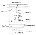
本実施例では、センサ部101の周辺に駆動回路を搭載し、画素を2次元に配置したエリアセンサについて説明する。より詳しくは、フォトダイオード113およびリセット用TFT110、バッファ用TFT111および選択用TFT112の駆動方法について説明する。本発明のエリアセンサ(表示装置)の回路図(概略図)を図3に示す。まず、画素が2次元に配列されたセンサ部101がある。そして、各々の画素のゲート信号線やリセット信号線を駆動するための駆動回路が、センサ部101の周りにそれぞれ配置されている。図3ではソース信号線駆動回路130、ゲート信号線用駆動回路132、センサ用ソース信号線駆動回路131、センサ用ゲート信号線駆動回路133がそれぞれ配置されている。
【0111】
図4は、図3に示すセンサ部101、センサ用ゲート信号線駆動回路133およびセンサ用ソース信号線駆動回路131を示し、画素102が有するフォトダイオード部104の駆動方法についてより詳しく説明する。センサ用ソース信号線駆動回路131は、バイアス用回路131a、サンプルホールド&信号処理用回路131b、信号出力用駆動回路131cを有している。
【0112】
バイアス用回路131aは、各画素のバッファ用TFT111と対になって、ソースフォロワ回路を形成する。図3において、バイアス用回路131aの下方には、サンプルホールド&信号処理用回路131bが配置されている。サンプルホールド&信号処理用回路131bでは、信号をいったん保存しておいたり、アナログ・デジタル変換を行ったり、雑音を低減したりするための回路である。そしてサンプルホールド&信号処理用回路131bの下方には、信号出力用駆動回路131cが配置されている。信号出力用駆動回路131cは、一時的に保存されていた信号を、順に出力していくための信号を出力している回路である。そして最終出力増幅用回路131dは、サンプルホールド&信号処理用回路131bと信号出力用駆動回路131cとから出力された信号を、外部に信号を出力ために増幅している。つまり信号を増幅しない場合は不必要であるが、現状では配置される場合が多い。
【0113】
次いで、各部分の回路図を示す。図5にi行目j列目の画素部回路135のフォトダイオード部104の回路図を示す。図5では、Pチャネル型リセット用TFT110、Pチャネル型選択用TFT112、Nチャネル型バッファ用TFT111、光電変換素子(ここでは、最も代表的なフォトダイオード113)から構成されている。また参考のために、Nチャネル型バイアス用TFT115も記述している。
【0114】
フォトダイオード113のPチャネル側端子は電源基準線116に、Nチャネル側端子は、バッファ用TFT111のゲート端子に接続されている。リセット用TFT110のゲート端子には、i行目リセット信号線(RGi)が接続され、ソース端子とドレイン端子は、j列目センサ用電源線とバッファ用TFT111のゲート端子に接続されている。選択用TFT112のゲート端子は、i行目選択信号線(SGi)に接続され、ソース端子とドレイン端子は、j列目センサ用信号出力線(SSj)とバッファ用TFT111に接続されている。バッファ用TFT111のソース端子とドレイン端子は、j列目センサ用電源線と選択用TFT112に接続されている。
【0115】
図5ではリセット用TFT110として、Pチャネル型TFTを用いているが、Nチャネル型でもよい。しかしNチャネル型の場合には、リセット動作のときに、ゲート・ソース間電圧が大きくとれない。よって、リセット用TFTが飽和領域で動作することになり、フォトダイオード113を十分に充電できない。すなわちリセット用TFT110は、Nチャネル型でも動作するが、Pチャネル型の方が望ましい。
【0116】
Pチャネル型選択用TFT112は、j列目センサ用信号出力線(SSj)とバッファ用TFT111の間に配置し、かつ、Pチャネル型を用いるのが望ましい。しかし、従来と同様に、Nチャネル型でも動作するため、Nチャネル型でも構わない。またセンサ用電源線(VB)とバッファ用TFT111の間に配置しても構わない。しかし、正確に信号を出力しにくいため、選択用TFT112は、j列目センサ用電源線(VB)とバッファ用TFT111の間に配置し、かつ、Pチャネル型を用いるのが望ましい。
【0117】
バッファ用TFT111は、図5では、Nチャネル型を用いているが、Pチャネル型を用いることも可能である。しかし、Pチャネル型バッファ用TFTとバイアス用TFTを組み合わせてソースフォロワ回路として動作させるためには、回路の接続方法を変更する必要がある。つまり図5の回路図において、バッファ用TFT141の極性を変えるだけでは、動作しないので、適宜周辺回路に応じた極性のTFTを用いるようにするとよい。
【0118】
そこで、Pチャネル型のバッファ用TFT111を用いた場合の回路構成の一例を図6に示す。図5と異なる点は、バッファ用TFT111とバイアス用TFT115の極性はPチャネル型である点、リセット用TFT110と選択用TFT112の極性がNチャネル型である点、フォトダイオード113の向きが逆になっている点、バイアス用TFT115およびフォトダイオード113のNチャネル側端子が電源線140に接続されている点が挙げられる。
【0119】
バッファ用TFT111にPチャネル型を用いる場合は、バイアス用TFT115もPチャネル型を用いる必要がある。バイアス用TFT115は、定電流源として動作させる必要があるからである。図6に示すフォトダイオード部104は、Nチャネル型リセット用TFT110、Nチャネル型選択用TFT112、Pチャネル型バッファ用TFT111、光電変換素子(ここでは、最も代表的なフォトダイオード113)から構成されている。
【0120】
フォトダイオード113はNチャネル側端子とPチャネル側端子を有し、Nチャネル側端子は電源線140に、Pチャネル側端子はPチャネル型バッファ用TFT111のゲート端子に接続されている。Nチャネル型リセット用TFT110のゲート端子には、i行目リセット信号線(RGi)が接続され、ソース端子とドレイン端子は、センサ用電源線(VB)とPチャネル型バッファ用TFT111のゲート端子に接続されている。Nチャネル型選択用TFT112のゲート端子は、i行目選択信号線(SGi)に接続され、ソース端子とドレイン端子は、j列目センサ用信号出力線(SSj)とPチャネル型バッファ用TFT111に接続されている。Pチャネル型バッファ用TFT111のソース端子とドレイン端子は、j列目センサ用信号出力線(SSj)とNチャネル型選択用TFT112に接続されている。Pチャネル型バイアス用TFT115のゲート端子は、バイアス信号線141に接続され、ソース端子とドレイン端子は、センサ用信号出力線(SSx)と電源線140に接続されている。
【0121】
リセット用TFT110は、Nチャネル型を用いている。しかしリセット用TFT110は、Pチャネル型でもよいが、リセット動作のとき、ゲート・ソース間電圧が大きくとれない。そのため、リセット用TFT110が飽和領域で動作することになり、フォトダイオード113を十分に充電できない。つまりリセット用TFT110は、Pチャネル型でも動作するが、Nチャネル型の方が望ましい。
【0122】
選択用TFT112については、センサ用信号出力線(SSx)とバッファ用TFT111の間に配置し、かつ、Nチャネル型を用いるのが望ましい。しかし、Pチャネル型でも構わない。また、センサ用電源線(VB)とバッファ用TFT111の間に配置しても構わない。ただし、正しく信号を出力しにくいため、選択用TFT112は、j列目センサ用信号出力線(SSj)とバッファ用TFT111の間に配置し、かつ、Nチャネル型を用いるのが望ましい。
【0123】
このように、図5と図6を比較すると分かるように、バッファ用TFTの極性が異なると、最適なTFTの構成、フォトダイオードの向きなども異なる。また図5では、選択用TFT112とリセット用TFT110の両方に、1本の電源線から電流を供給している。図6では、選択用TFT112とリセット用TFT110の両方に、1本の電源基準線から電流を供給している。このように、フォトダイオードの向きとバッファ用TFTの極性をあわせることにより、配線を共有することができる。
【0124】
次いで図7には、バイアス用回路131a、サンプルホールド&信号処理用回路131b、信号出力線用駆動回路131cのj列目周辺部回路136の回路図を示す。バイアス用回路131aには、バイアス用TFT115が配置されている。その極性は、各画素のバッファ用TFT111の極性と同じである。
【0125】
図7に示すバイアス用TFT115は、Nチャネル型TFTである。バイアス用TFT115のゲート端子には、バイアス信号線141が接続され、ソース端子とドレイン端子は、j列目センサ用信号出力線(SSj)145と電源基準線116に接続されている(バイアス用TFT115がPチャネル型の場合は、電源基準線116のかわりに、電源線140に接続される)。Nチャネル型バイアス用TFT115は、各画素のバッファ用TFT111と対になって、ソースフォロワ回路として動作する。
【0126】
転送用TFT148のゲート端子には、転送信号線142が接続され、ソース端子とドレイン端子は、j列目センサ用信号出力線(SSj)145とコンデンサ149にそれぞれ接続されている。転送用TFT148は、j列目センサ用信号出力線(SSj)145の電位をコンデンサ149に転送する場合に動作する。また、Pチャネル型の転送用TFT148を追加して、Nチャネル型転送用TFT148と並列に接続してもよい。コンデンサ149は、転送用TFT148と電源基準線116に接続されている。コンデンサ149の役割は、j列目センサ用信号出力線(SSj)145から出力される信号を一時的に蓄積することである。放電用TFT150のゲート端子は、プリ放電信号線143に接続され、ソース端子とドレイン端子は、コンデンサ149と電源基準線116にそれぞれ接続されている。放電用TFT150は、j列目センサ用信号出力線(SSj)145の電位をコンデンサ149に入力する前に、コンデンサ149に蓄積されている電荷を放電するように動作する。
【0127】
なお、アナログ・デジタル信号変換回路や雑音低減回路などを配置することも可能である。
【0128】
そして、コンデンサ149と最終出力線144の間に、最終選択用TFT152が接続される。最終選択用TFT152のソース端子とドレイン端子は、コンデンサ149と最終出力線144にそれぞれ接続され、ゲート端子はj列目最終選択線146に接続される。最終選択線は、センサ部においてマトリクス状に配置されており、1列目からx列目まで順にスキャンされていく。そしてj列目最終出力線144が選択され、最終選択用TFT152が導通状態になると、コンデンサ149の電位とj列目最終出力線144の電位が等しくなる。その結果、コンデンサ149に蓄積していた信号を最終出力線144に出力することができる。
【0129】
ただし、最終出力線144に信号を出力する前に、最終出力線144に電荷が蓄積されていると、その電荷によって最終出力線144に信号を出力したときの電位が影響を受ける。そこで、最終出力線144に信号を出力する前に、最終出力線144の電位を、ある特定の電位値に初期化することが必要である。
【0130】
図7には、最終出力線144と電源基準線116の間に、最終リセット用TFT151を配置している図を示している。そして、最終リセット用TFT151のゲート端子には、j列目最終リセット線147が接続されている。そして、j列目最終選択線146を選択する前に、j列目最終リセット線147を選択し、最終出力線144の電位を電源基準線116の電位に初期化する。その後、j列目最終選択線146を選択し、最終出力線144に、コンデンサ149に蓄積されていた信号を出力する。
【0131】
最終出力線144に出力される信号は、そのまま外部に取り出しても良い。しかし、信号が微弱であるため、外部に取り出す前に増幅しておく場合が多い。図8には、信号を増幅するための回路として、最終出力増幅用回路131dの回路を示す。信号を増幅するための回路としては、演算増幅器などさまざまな種類があるが、本実施例では、最も簡単な回路構成として、ソースフォロワ回路を示す。
【0132】
図8には、ソースフォロワ回路がNチャネル型の場合の回路図を示す。最終出力増幅用回路131dへの入力は、最終出力線144を介して行われる。最終出力線144は、センサ部においてマトリクス状に配置されており、その1列目から順に信号が出力される。その信号は、最終出力増幅用回路131dにおいて増幅されて、外部に出力する。最終出力線144は、最終出力増幅向け増幅用TFT154のゲート端子に接続される。最終出力増幅向け増幅用TFT154のドレイン端子は、電源線153に接続され、ソース端子は、出力端子となる。最終出力増幅向けバイアス用TFT155のゲート端子は、最終出力増幅用バイアス信号線156と接続される。また最終出力増幅向けバイアス用TFT155のソース端子とドレイン端子は、一方は電源基準線157に接続され、もう一方は最終出力増幅向け増幅用TFT154のソース端子に接続される。
【0133】
図9には、ソースフォロワ回路がPチャネル型の場合の回路図を示す。最終出力線144は、最終出力増幅向け増幅用TFT154のゲート端子に接続される。最終出力増幅向け増幅用TFT154のドレイン端子は、電源基準線157に接続され、ソース端子は、出力端子となる。最終出力増幅向けバイアス用TFT155のゲート端子は、最終出力増幅用バイアス信号線156と接続される。また最終出力増幅向けバイアス用TFT155のソース端子とドレイン端子は、一方は電源線153に接続され、もう一方は最終出力増幅向け増幅用TFT154のソース端子に接続される。なお最終出力増幅用バイアス信号線156の電位は、Nチャネル型を用いた場合の最終出力増幅用バイアス信号線156の電位とは異なる。
【0134】
図8と図9では、ソースフォロワ回路を1段のみで構成していた。しかし、複数段で構成しても良い。例えば、2段で構成する場合は、1段目の出力端子を2段目の入力端子に接続すればよい。また各々の段において、Nチャネル型を用いても、Pチャネル型を用いても、どちらでも良い。つまりソースフォロワ回路は、設計者が自由に設計することが出来る。
【0135】
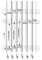
次いで、信号のタイミングチャートについて説明する。始めに、図4と図5に示す回路における信号のタイミングチャートについて、図10を用いて説明する。リセット信号線RGは、1行目からy行目まで順にスキャンしていく。そして、再び同じ行を選択するまでの期間が1フレーム期間に相当する。
【0136】
選択信号線SGも、同様に、1行目からy行目まで順にスキャンしていく。ただし、リセット信号線RGをスキャンし始めるタイミングよりも、選択信号線SGをスキャンし始めるタイミングの方が遅い。例えば、i行目の画素102に着目すると、i行目リセット信号線SRiが選択されて、その後、i行目選択信号線SGiが選択される。次いでi行目ゲート信号線SSiが選択されると、i行目の画素102から信号が出力される。なお画素102がリセットされてから、信号を出力する時までの期間は蓄積時間に相当する。蓄積時間では、フォトダイオードで光によって生成される電荷を蓄積している。各行で、リセットされるタイミングと信号を出力するタイミングは異なっているが、蓄積時間は全ての行の画素102で等しくなる。
【0137】
次に、図7に示す回路図における信号のタイミングチャートを図11に示す。繰り返しの動作になるため、本実施例では一例として、i行目の選択信号線SGiが選択されたときを説明する。まず、i行目の選択信号線SGiが選択された後、プリ放電信号線171を選択し、放電用TFT167を導通状態にする。その後、転送信号線170を選択する。すると、i行目の画素102から、各列の信号が各列のコンデンサ149に出力される。
【0138】
i行目に設けられた全ての画素102の信号を、各列のコンデンサ149に蓄積した後、最終出力線144に各列の信号を順に出力していく。転送信号線142が非選択されると、信号出力用駆動回路131cにより、1列目からx列目までをスキャンしていく。まず1列目の最終リセット線を選択し、最終リセット用TFT151を導通状態にし、最終出力線144を電源基準線116の電位に初期化する。その後、1列目の最終選択線を選択し、最終選択用TFT152を導通状態にし、1列目のコンデンサ149の信号を最終出力線144に出力する。
【0139】
次に、2列目の最終リセット線を選択し、最終リセット用TFT151を導通状態にし、最終出力線144を電源基準線164の電位に初期化する。その後、2列目の最終選択線を選択し、最終選択用TFT152を導通状態にし、2列目のコンデンサ149の信号を最終出力線144に出力する。その後は、同様の動作を繰り返していく。
【0140】
j列目の場合も、j列目最終リセット線147を選択し、最終リセット用TFT151を導通状態にし、最終出力線144を電源基準線116の電位に初期化する。その後、j列目最終選択線146を選択し、最終選択用TFT152を導通状態にし、j列目のコンデンサ149の信号を最終出力線144に出力する。
【0141】
次に、(j+1)列目の最終リセット線を選択し、最終リセット用TFT151を導通状態にし、最終出力線144を電源基準線116の電位に初期化する。その後、(j+1)列目最終選択線146を選択し、最終選択用TFT152を導通状態にし、(j+1)列目のコンデンサ149の信号を最終出力線144に出力する。その後は、同様の動作を繰り返し、全ての列の信号を最終出力線144に、順次出力していく。そのあいだ、バイアス信号線141は、一定に保たれている。そして最終出力線144に出力された信号は、最終出力増幅用回路131dで増幅され、外部へ出力されていく。
【0142】
次に、(i+1)行目ゲート信号線が選択される。すると、i行目ゲート信号線が選択されたのと同様に、動作する。そして、(i+2)行目のゲート信号線が選択され、同様の動作を繰り返していく。
【0143】
なお、光電変換などを行うセンサ部については、通常使用されているPN型のフォトダイオードの他に、PIN型のダイオード、アバランシェ型ダイオード、NPN埋め込み型ダイオード、ショットキー型ダイオード、X線用のフォトコンダクタ、赤外線用のセンサなどでもよい。また蛍光材やシンチレータにより、X線を光に変換した後、その光を読み取ってもよい。
【0144】
上述のように、光電変換素子は、ソースフォロワ回路の入力端子に接続されることが多い。しかし、フォトゲート型の光電変換素子を用いる場合には、スイッチを間に挟んでもよい。また、対数変換型の光電変換素子を用いる場合には、光強度の対数値なるように処理した後の信号を入力端子に入力してもよい。
【0145】
なお、本実施の形態では、画素が2次元に配置されたエリアセンサについて述べたが、画素が1次元に配置されたラインセンサにも応用することも出来る。
【0146】
なお本実施例は、実施の形態1〜5と自由に組み合わせることが可能である。
【0147】
(実施例2)
本実施例では、図2に示すところのEL素子106の動作を制御している、スイッチング用TFT105及びEL駆動用TFT106の駆動方法について説明する。なおセンサ部101の構成は実施例1で示した構成と同じであるので、図1及び図2を参照するとよい。
【0148】
図12に本実施例のエリアセンサの上面図を示す。120はソース信号線駆動回路、122はゲート信号線駆動回路であり、共にスイッチング用TFT105及びEL駆動用TFT106の駆動を制御している。また121はセンサ用ソース信号線駆動回路、123はセンサ用ゲート信号線駆動回路であり、共にリセット用TFT110、バッファ用TFT111及び選択用TFT112の駆動を制御している。なお本明細書において、ソース信号線駆動回路120、ゲート信号線駆動回路122、センサ用ソース信号線駆動回路121、センサ用ゲート信号線駆動回路123を駆動部と呼ぶ。
【0149】
ソース信号線駆動回路120は、シフトレジスタ120a、ラッチ(A)120b、ラッチ(B)120cを有している。ソース信号線駆動回路120において、シフトレジスタ120aにクロック信号(CLK)およびスタートパルス(SP)が入力される。シフトレジスタ120aは、これらのクロック信号(CLK)およびスタートパルス(SP)に基づきタイミング信号を順に発生させ、後段の回路へタイミング信号を順次供給する。
【0150】
なおシフトレジスタ120aからのタイミング信号を、バッファ等(図示せず)によって緩衝増幅し、後段の回路へ緩衝増幅したタイミング信号を順次供給しても良い。タイミング信号が供給される配線には、多くの回路あるいは素子が接続されているために負荷容量(寄生容量)が大きい。この負荷容量が大きいために生ずるタイミング信号の立ち上がりまたは立ち下がりの”鈍り”を防ぐために、このバッファが設けられる。
【0151】
シフトレジスタ120aからのタイミング信号は、ラッチ(A)120bに供給される。ラッチ(A)120bは、デジタル信号(digital signals)を処理する複数のステージのラッチを有している。ラッチ(A)120bは、前記タイミング信号が入力されると同時に、デジタル信号を順次書き込み、保持する。
【0152】
なお、ラッチ(A)120bにデジタル信号を取り込む際に、ラッチ(A)120bが有する複数のステージのラッチに、順にデジタル信号を入力しても良い。しかし本発明はこの構成に限定されない。ラッチ(A)120bが有する複数のステージのラッチをいくつかのグループに分け、グループごとに並行して同時にデジタル信号を入力する、いわゆる分割駆動を行っても良い。なおこのときのグループの数を分割数と呼ぶ。例えば4つのステージごとにラッチをグループに分けた場合、4分割で分割駆動すると言う。
【0153】
ラッチ(A)120bの全ステージのラッチへのデジタル信号の書き込みが一通り終了するまでの時間を、ライン期間と呼ぶ。すなわち、ラッチ(A)120b中で一番左側のステージのラッチにデジタル信号の書き込みが開始される時点から、一番右側のステージのラッチにデジタル信号の書き込みが終了する時点までの時間間隔がライン期間である。実際には、上記ライン期間に水平帰線期間が加えられた期間をライン期間に含むことがある。
【0154】
1ライン期間が終了すると、ラッチ(B)120cにラッチシグナル(Latch Signal)が供給される。この瞬間、ラッチ(A)120bに書き込まれ保持されているデジタル信号は、ラッチ(B)120cに一斉に送出され、ラッチ(B)120cの全ステージのラッチに書き込まれ、保持される。
【0155】
デジタル信号をラッチ(B)120cに送出し終えたラッチ(A)120bは、シフトレジスタ120aからのタイミング信号に基づき、再びデジタル信号の書き込みを順次行う。
【0156】
この2順目の1ライン期間中には、ラッチ(B)120bに書き込まれ、保持されているデジタル信号がソース信号線(S1〜Sx)に入力される。
【0157】
一方、ゲート信号線駆動回路122は、それぞれシフトレジスタ、バッファ(いずれも図示せず)を有している。また場合によっては、ゲート信号線駆動回路122が、シフトレジスタ、バッファの他にレベルシフトを有していても良い。
【0158】
ゲート信号線駆動回路122において、シフトレジスタ(図示せず)からのゲート信号がバッファ(図示せず)に供給され、対応するゲート信号線に供給される。ゲート信号線(G1〜Gy)には、それぞれ1ライン分の画素のスイッチング用TFT105のゲート電極が接続されており、1ライン分全ての画素のスイッチング用TFT105を同時にオンの状態にしなくてはならないので、バッファは大きな電流を流すことが可能なものが用いられる。
【0159】
なおソース信号線駆動回路とゲート信号線駆動回路の数、構成及びその動作は、本実施例で示した構成に限定されない。本発明のエリアセンサは、公知のソース信号線駆動回路及びゲート信号線駆動回路を用いることが可能である。
【0160】
次に、センサ部のスイッチング用TFT105及びEL駆動用TFT106を、デジタル方式で駆動させた場合のタイミングチャートを図13に示す。
【0161】
センサ部101の全ての画素が一通り発光するまでの期間を1フレーム期間(F)と呼ぶ。フレーム期間はアドレス期間Taとサステイン期間Tsとに分けられる。アドレス期間とは、1フレーム期間中、全ての画素にデジタル信号を入力する期間である。サステイン期間(点灯期間とも呼ぶ)とは、アドレス期間において画素に入力されたデジタル信号によって、EL素子を発光又は非発光の状態にし、表示を行う期間を示している。
【0162】
電源供給線(V1〜Vx)の電位は所定の電位(電源電位)に保たれている。
【0163】
まずアドレス期間Taにおいて、EL素子106の対向電極の電位は、電源電位と同じ高さに保たれている。
【0164】
そしてゲート信号線G1に入力されるゲート信号によって、ゲート信号線G1に接続されている全てのスイッチング用TFT105がオンの状態になる。次に、ソース信号線駆動回路120からソース信号線(S1〜Sx)にデジタル信号が入力される。ソース信号線(S1〜Sx)に入力されたデジタル信号は、オンの状態のスイッチング用TFT105を介してEL駆動用TFT106のゲート電極に入力される。
【0165】
次にゲート信号線G2に入力されるゲート信号によって、ゲート信号線G2に接続されている全てのスイッチング用TFT105がオンの状態になる。次に、ソース信号線駆動回路120からソース信号線(S1〜Sx)にデジタル信号が入力される。ソース信号線(S1〜Sx)に入力されたデジタル信号は、オンの状態のスイッチング用TFT105を介してEL駆動用TFT106のゲート電極に入力される。
【0166】
上述した動作をゲート信号線Gyまで繰り返し、全ての画素102のEL駆動用TFT106のゲート電極にデジタル信号が入力され、アドレス期間が終了する。
【0167】
アドレス期間Taが終了すると同時にサステイン期間となる。サステイン期間において、全てのスイッチング用TFT105は、オフの状態となる。
【0168】
そしてサステイン期間が開始されると同時に、全てのEL素子の対向電極の電位は、電源電位が画素電極に与えられたときにEL素子が発光する程度に、電源電位との間に電位差を有する高さになる。なお本明細書において、画素電極と対向電極の電位差をEL駆動電圧と呼ぶ。また各画素が有するEL駆動用TFT106のゲート電極に入力されたデジタル信号によってEL駆動用TFT106はオンの状態になっている。よって電源電位がEL素子の画素電極に与えられ、全ての画素が有するEL素子は発光する。
【0169】
サステイン期間が終了すると同時に、1つのフレーム期間が終了する。本発明では、全てのサンプリング期間ST1〜STyにおいて画素が発光する必要があり、よって本実施例の駆動方法の場合、サステイン期間内にセンサフレーム期間SFが含まれていることが重要である。
【0170】
なお本実施例では、単色の画像を読み込むエリアセンサの駆動方法について説明したが、カラー画像を読み込む場合も同様である。ただしカラー画像を読み込むエリアセンサの場合、1つのフレーム期間をRGBに対応した3つのサブフレーム期間に分割し、各サブフレーム期間においてアドレス期間とサステイン期間とを設ける。そしてR用のサブフレーム期間のアドレス期間では、Rに対応する画素のEL素子だけ発光するようなデジタル信号を全ての画素に入力し、サステイン期間においてRのEL素子だけ発光を行う。G用、B用のサブフレーム期間においても同様に、各サステイン期間において、各色に対応する画素のEL素子のみが発光を行うようにする。
【0171】
そしてカラー画像を読み込むエリアセンサの場合、RGBに対応した3つのサブフレーム期間の各サステイン期間は、R用、G用、B用センサフレーム期間(SFr、SFg、SFb)をそれぞれ含んでいることが重要である。
【0172】
なお本実施例は、実施の形態1〜5、及び実施例1と自由に組み合わせることが可能である。
【0173】
(実施例3)
本実施例では、センサ部101において画像を表示するときの、スイッチング用TFT105及びEL駆動用TFT106(EL素子部103)の駆動方法について説明する。なおセンサ部101の構成は実施例1で示した構成と同じであるので、図1及び図2を参照すればよい。
【0174】
図14に、本発明のエリアセンサにおいて、デジタル方式でセンサ部101に画像を表示するときのタイミングチャートを示す。
【0175】
まず、1フレーム期間(F)をn個のサブフレーム期間(SF1〜SFn)に分割する。階調数が多くなるにつれて1フレーム期間におけるサブフレーム期間の数も増える。なおエリアセンサのセンサ部が画像を表示する場合、1フレーム期間(F)とは、センサ部101の全ての画素が1つの画像を表示する期間を指す。
【0176】
本実施例の場合、フレーム期間は1秒間に60以上設けることが好ましい。1秒間に表示される画像の数を60以上にすることで、視覚的にフリッカ等の画像のちらつきを抑えることが可能になる。
【0177】
サブフレーム期間はアドレス期間(Ta)とサステイン期間(Ts)とに分けられる。アドレス期間とは、1サブフレーム期間中、全ての画素にデジタルビデオ信号を入力する期間である。なおデジタルビデオ信号とは、画像情報を有するデジタルの信号である。サステイン期間(点灯期間とも呼ぶ)とは、アドレス期間において画素に入力されたデジタルビデオ信号によって、EL素子を発光又は非発光の状態にし、表示を行う期間を示している。なおデジタルビデオ信号とは、画像情報を有するデジタル信号を意味する。
【0178】
SF1〜SFnが有するアドレス期間(Ta)をそれぞれTa1〜Tanとする。SF1〜SFnが有するサステイン期間(Ts)をそれぞれTs1〜Tsnとする。
【0179】
電源供給線(V1〜Vx)の電位は所定の電位(電源電位)に保たれている。
【0180】
まずアドレス期間Taにおいて、EL素子106対向電極の電位は、電源電位と同じ高さに保たれている。
【0181】
次にゲート信号線G1に入力されるゲート信号によって、ゲート信号線G1に接続されている全てのスイッチング用TFT105がオンの状態になる。次に、ソース信号線駆動回路102からソース信号線(S1〜Sx)にデジタルビデオ信号が入力される。デジタルビデオ信号は「0」または「1」の情報を有しており、「0」と「1」のデジタルビデオ信号は、一方がHi、他方がLoの電圧を有する信号である。
【0182】
そしてソース信号線(S1〜Sx)に入力されたデジタルビデオ信号は、オンの状態のスイッチング用TFT105を介して、EL駆動用TFT106のゲート電極に入力される。
【0183】
次にゲート信号線G1に接続されている全てのスイッチング用TFT105がオフの状態になり、ゲート信号線G2に入力されるゲート信号によって、ゲート信号線G2に接続されている全てのスイッチング用TFT105がオンの状態になる。次に、ソース信号線駆動回路102からソース信号線(S1〜Sx)にデジタルビデオ信号が入力される。ソース信号線(S1〜Sx)に入力されたデジタルビデオ信号は、オンの状態のスイッチング用TFT105を介して、EL駆動用TFT106のゲート電極に入力される。
【0184】
上述した動作をゲート信号線Gyまで繰り返し、全ての画素102のEL駆動用TFT106のゲート電極にデジタルビデオ信号が入力され、アドレス期間が終了する。
【0185】
アドレス期間Taが終了すると同時にサステイン期間Tsとなる。サステイン期間において、全てのスイッチング用TFT105はオフの状態になる。サステイン期間において、全てのEL素子の対向電極の電位は、電源電位が画素電極に与えられたときにEL素子が発光する程度に、電源電位との間に電位差を有する高さになる。
【0186】
本実施例では、デジタルビデオ信号が「0」の情報を有していた場合、EL駆動用TFT106はオフの状態になる。よってEL素子の画素電極は対向電極の電位に保たれたままである。その結果、「0」の情報を有するデジタルビデオ信号が入力された画素において、EL素子106は発光しない。
【0187】
逆にデジタルビデオ信号が「1」の情報を有していた場合、EL駆動用TFT106はオンの状態になる。よって電源電位がEL素子106の画素電極に与えられる。その結果、「1」の情報を有するデジタルビデオ信号が入力された画素が有するEL素子106は発光する。
【0188】
このように、画素に入力されるデジタルビデオ信号の有する情報によって、EL素子が発光または非発光の状態になり、画素は表示を行う。
【0189】
サステイン期間が終了すると同時に、1つのサブフレーム期間が終了する。そして次のサブフレーム期間が出現し、再びアドレス期間に入り、全画素にデジタルビデオ信号を入力したら、再びサステイン期間に入る。なお、サブフレーム期間SF1〜SFnの出現する順序は任意である。
【0190】
以下、残りのサブフレーム期間においても同様の動作を繰り返し、表示を行う。n個のサブフレーム期間が全て終了したら、1つの画像が表示され、1フレーム期間が終了する。1フレーム期間が終了すると次のフレーム期間のサブフレーム期間が出現し、上述した動作を繰り返す。
【0191】
本発明において、n個のサブフレーム期間がそれぞれ有するアドレス期間(Ta1〜Tan)の長さは全て同じである。またn個のサステイン期間Ts1、…、Tsnの長さの比は、Ts1:Ts2:Ts3:…:Ts(n−1):Tsn=20:2-1:2-2:…:2-(n-2):2-(n-1)で表される。
【0192】
各画素の階調は、1フレーム期間においてどのサブフレーム期間を発光させるかによって決まる。例えば、n=8のとき、全部のサステイン期間で発光した場合の画素の輝度を100%とすると、Ts1とTs2において画素が発光した場合には75%の輝度が表現でき、Ts3とTs5とTs8を選択した場合には16%の輝度が表現できる。
【0193】
なお本実施例は、実施の形態1〜5、実施例1、2と自由に組み合わせることが可能である。
【0194】
(実施例4)
実施例1及び2では、アドレス期間において対向電極の電位を電源電位と同じ電位に保っていたため、EL素子は発光しなかった。しかし本発明はこの構成に限定されない。画素電極に電源電位が与えられたときにEL素子が発光する程度の電位差を、対向電位と電源電位との間に常に設け、アドレス期間においても表示期間と同様に表示を行うようにしても良い。
【0195】
ただしEL素子をエリアセンサの光源として用いる実施例1と本実施例を組み合わせる場合、単色の画像を読み込むエリアセンサでは、フレーム期間内にセンサフレーム期間SFが含まれていることが重要である。またカラー画像を読み込むエリアセンサでは、RGBに対応した3つのサブフレーム期間が、それぞれR用、G用、B用のセンサフレーム期間に含まれていることが重要である。
【0196】
またセンサ部に画像を表示する実施例2と本実施例を組み合わせる場合、サブフレーム期間全体が実際に表示を行う期間となるので、サブフレーム期間の長さを、SF1:SF2:SF3:…:SF(n−1):SFn=20:2-1:2-2:…:2-(n-2):2-(n-1)となるように設定する。上記構成により、アドレス期間を発光させない駆動方法に比べて、高い輝度の画像が得られる。
【0197】
なお本実施例は、実施の形態1〜5、実施例1〜3と自由に組み合わせることが可能である。
【0198】
(実施例5)
本実施例では、図2に示すEL素子107の動作を制御している、スイッチング用TFT105及びEL駆動用TFT106の駆動方法の、実施例1とは異なる例について説明する。なおセンサ部の構成は実施例1で示した構成と同じであるので、図1及び図2を参照すればよい。
【0199】
図15に本実施例のエリアセンサの上面図を示す。130はソース信号線駆動回路、126はゲート信号線駆動回路であり、共にスイッチング用TFT105及びEL駆動用TFT106の駆動を制御している。また125はセンサ用ソース信号線駆動回路、127はセンサ用ゲート信号線駆動回路であり、共にリセット用TFT110、バッファ用TFT111及び選択用TFT112の駆動を制御している。本実施例ではソース信号線駆動回路とゲート信号線駆動回路とを1つずつ設けたが、本発明はこの構成に限定されない。ソース信号線駆動回路を2つ設けても良い。また、ゲート信号線駆動回路を2つ設けても良い。
【0200】
なお本明細書において、ソース信号線駆動回路130、ゲート信号線駆動回路126、センサ用ソース信号線駆動回路125、センサ用ゲート信号線駆動回路127を駆動部と呼ぶ。
【0201】
ソース信号線駆動回路130は、シフトレジスタ130a、レベルシフト130b、サンプリング回路130cを有している。なおレベルシフトは必要に応じて用いればよく、必ずしも用いなくとも良い。また本実施例においてレベルシフトはシフトレジスタ130aとサンプリング回路130cとの間に設ける構成としたが、本発明はこの構成に限定されない。またシフトレジスタ130aの中にレベルシフト130bが組み込まれている構成にしても良い。
【0202】
クロック信号(CLK)、スタートパルス信号(SP)がシフトレジスタ130aに入力される。シフトレジスタ130aからアナログの信号(アナログ信号)をサンプリングするためのサンプリング信号が出力される。出力されたサンプリング信号はレベルシフト130bに入力され、その電位の振幅が大きくなって出力される。
【0203】
レベルシフト130bから出力されたサンプリング信号は、サンプリング回路130cに入力される。そしてサンプリング回路130cに入力されるアナログ信号がサンプリング信号によってそれぞれサンプリングされ、ソース信号線S1〜Sxに入力される。
【0204】
一方、ゲート信号線駆動回路126は、それぞれシフトレジスタ、バッファ(いずれも図示せず)を有している。また場合によっては、ゲート信号線駆動回路126が、シフトレジスタ、バッファの他にレベルシフトを有していても良い。
【0205】
ゲート信号線駆動回路126において、シフトレジスタ(図示せず)からのゲート信号がバッファ(図示せず)に供給され、対応するゲート信号線に供給される。ゲート信号線G1〜Gyには、それぞれ1ライン分の画素のスイッチング用TFT105のゲート電極が接続されており、1ライン分全ての画素のスイッチング用TFT105を同時にオンの状態にしなくてはならないので、バッファは大きな電流を流すことが可能なものが用いられる。
【0206】
なおソース信号線駆動回路とゲート信号線駆動回路の数、構成及びその動作は、本実施例で示した構成に限定されない。本発明のエリアセンサは、公知のソース信号線駆動回路及びゲート信号線駆動回路を用いることが可能である。
【0207】
次に、センサ部のスイッチング用TFT105及びEL駆動用TFT106を、アナログ方式で駆動させた場合のタイミングチャートを図16に示す。センサ部101の全ての画素が一通り発光するまでの期間を1フレーム期間Fと呼ぶ。1ライン期間Lは、1つのゲート信号線が選択されてから、その次に別のゲート信号線が選択されるまでの期間を意味する。図2に示したエリアセンサの場合、ゲート信号線はy本あるので、1フレーム期間中にy個のライン期間L1〜Lyが設けられている。
【0208】
解像度が高くなるにつれて1フレーム期間中のライン期間の数も増え、駆動回路を高い周波数で駆動しなければならなくなる。
【0209】
まず電源電圧線V1〜Vxは一定の電源電位に保たれている。そしてEL素子106の対向電極の電位である対向電位も一定の電位に保たれている。電源電位は、電源電位がEL素子106の画素電極に与えられるとEL素子106が発光する程度に、対向電位との間に電位差を有している。
【0210】
第1のライン期間L1において、ゲート信号線駆動回路126からゲート信号線G1に入力されるのゲート信号によって、ゲート信号線G1に接続された全てのスイッチング用TFT105はオンの状態になる。そして、ソース信号線S1〜Sxに順にソース信号線駆動回路130からアナログ信号が入力される。ソース信号線S1〜Sxに入力されたアナログ信号は、スイッチング用TFT105を介してEL駆動用TFT106のゲート電極に入力される。
【0211】
EL駆動用TFT106のチャネル形成領域を流れる電流の大きさは、そのゲート電極に入力される信号の電位の高さ(電圧)によって制御される。よって、EL素子106の画素電極に与えられる電位は、EL駆動用TFT106のゲート電極に入力されたアナログ信号の電位の高さによって決まる。そしてEL素子105はアナログ信号の電位に制御されて発光を行う。なお本実施例の場合、全ての画素に入力されるアナログ信号は、同じ高さの電位に保たれている。
【0212】
ソース信号線S1〜Sxへのアナログ信号の入力が終了すると、第1のライン期間L1が終了する。なお、ソース信号線S1〜Sxへのアナログ信号の入力が終了するまでの期間と水平帰線期間とを合わせて1つのライン期間としても良い。そして次に第2のライン期間L2となり、ゲート信号線G1に接続された全てのスイッチング用TFT105はオフの状態になり、ゲート信号線G2に入力されるゲート信号によって、ゲート信号線G2に接続された全てのスイッチング用TFT105はオンの状態になる。そして第1のライン期間L1と同様に、ソース信号線S1〜Sxに順にアナログ信号が入力される。
【0213】
そして上述した動作をゲート信号線Gyまで繰り返し、全てのライン期間L1〜Lyが終了する。全てのライン期間L1〜Lyが終了すると、1フレーム期間が終了する。1フレーム期間が終了することで、全ての画素が有するEL素子は発光を行う。なお全てのライン期間L1〜Lyと垂直帰線期間とを合わせて1フレーム期間としても良い。
【0214】
なお本実施例では、単色の画像を読み込むエリアセンサの駆動方法について説明したが、カラー画像を読み込む場合も同様である。ただしカラー画像を読み込むエリアセンサの場合、1つのフレーム期間をRGBに対応した3つのサブフレーム期間に分割する。そしてR用のサブフレーム期間では、Rに対応する画素のEL素子だけ発光するようなアナログ信号を全ての画素に入力し、RのEL素子だけ発光を行う。G用、B用のサブフレーム期間においても同様に、各色に対応する画素のEL素子のみが発光を行うようにする。
【0215】
そしてカラー画像を読み込むエリアセンサの場合、RGBに対応した3つのサブフレーム期間の各サステイン期間は、R用、G用、B用センサフレーム期間(SFr、SFg、SFb)を含んでいることが重要である。
【0216】
なお本実施例の駆動方法において、センサ部101に画像を表示させる場合は、アナログ信号の代わりに画像情報を有するアナログのビデオ信号(アナログビデオ信号)を入力すると、センサ部101に画像を表示することが可能である。
【0217】
なお本実施例は、実施の形態1〜5、実施例1〜4と自由に組み合わせることが可能である。
【0218】
(実施例6)
本実施例では、本発明のエリアセンサのセンサ部における断面図について説明する。
【0219】
図17に本実施例のエリアセンサの断面図を示す。401はスイッチング用TFT、402はEL駆動用TFT、403はリセット用TFT、404はバッファ用TFT、405は選択用TFTである。
【0220】
また、406はカソード電極、407は光電変換層、408はアノード電極である。カソード電極406と、光電変換層407と、アノード電極408とによって、フォトダイオード421が形成される。414はセンサ用配線であり、アノード電極408と外部の電源とを接続している。
【0221】
また409は画素電極(陰極)、410は発光層、411は正孔注入層、412は対向電極(陽極)である。画素電極(陰極)409と、発光層410と、正孔注入層411と、対向電極(陽極)412とでEL素子422が形成される。なお413はバンクであり、隣り合う画素同士の発光層410を区切っている。
【0222】
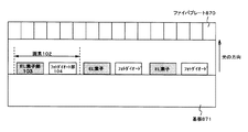
432は層間絶縁膜であり、431は光ファイバプレート、またはガラスファイバプレートである。423は被写体であり、EL素子422から発せられた光は、被写体423において反射し、フォトダイオード421に照射される。本実施例では、被写体423を基板430のTFTが形成されている側に設ける。
【0223】
本実施例においては、スイッチング用TFT401、EL駆動用TFT402、バッファ用TFT404、選択用TFT405は全てNチャネル型TFTである。またリセット用TFT403はPチャネル型TFTである。なお本発明はこの構成に限定されない。よってスイッチング用TFT401、EL駆動用TFT402、バッファ用TFT404、選択用TFT405、リセット用TFT403は、Nチャネル型TFTとPチャネル型TFTのどちらでも良い。
【0224】
ただし本実施例のように、EL駆動用TFT402のソース領域またはドレイン領域がEL素子の陰極と電気的に接続されている場合、EL駆動用TFT402はNチャネル型TFTであることが望ましい。また逆に、EL駆動用TFT402のソース領域またはドレイン領域がEL素子の陽極と電気的に接続されている場合、EL駆動用TFT402はPチャネル型TFTであることが望ましい。
【0225】
また、本実施例のように、リセット用TFT403のドレイン領域がフォトダイオード421のカソード電極406とが電気的に接続されている場合、リセット用TFT403はPチャネル型TFT、バッファ用TFT404はNチャネル型TFTであることが望ましい。逆にリセット用TFT403のドレイン領域がフォトダイオード421のアノード電極408と電気的に接続され、センサ用配線414がカソード電極406と接続されている場合、リセット用TFT403はNチャネル型TFT、バッファ用TFT404はPチャネル型TFTであることが望ましい。
【0226】
なお本実施例は、実施の形態1〜5、実施例1〜実施例5と自由に組み合わせることが可能である。
【0227】
(実施例7)
本実施例では、本発明のエリアセンサのセンサ部における断面図の実施例6とは異なる例について説明する。
【0228】
図18に本実施例のエリアセンサの断面図を示す。501はスイッチング用TFT、502はEL駆動用TFT、503はリセット用TFT、504はバッファ用TFT、505は選択用TFTである。
【0229】
また、506はカソード電極、507は光電変換層、508はアノード電極である。カソード電極506と、光電変換層507と、アノード電極508とによって、フォトダイオード521が形成される。514はセンサ用配線であり、アノード電極508と外部の電源とを電気的に接続している。また、フォトダイオード521のカソード電極506とリセット用TFT503のドレイン領域とは電気的に接続されている。
【0230】
また509は画素電極(陽極)、510はEL層、511は対向電極(陰極)である。画素電極(陽極)509と、EL層510と、対向電極(陰極)511とでEL素子522が形成される。なお512はバンクであり、隣り合う画素同士のEL層510を区切っている。
【0231】
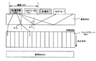
523は被写体であり、EL素子522から発せられた光が被写体523上で反射し、フォトダイオード521に照射される。本実施例では、実施例6と異なり、被写体を基板530のTFTが形成されていない側に設ける。
【0232】
本実施例では、基板530として、光ファイバプレート、またはガラスファイバプレートを用いることが好ましい。また実施例10にあるように、基板をガラス基板、石英基板、シリコン基板、金属基板(SUS基板)もしくはセラミックス基板とし、センサ部を形成してから、光ファイバプレートを基板上に接着することもできる。
【0233】
本実施例において、スイッチング用TFT501、バッファ用TFT504、選択用TFT505は全てNチャネル型TFTである。またEL駆動用TFT502、リセット用TFT503はPチャネル型TFTである。なお本発明はこの構成に限定されない。よってスイッチング用TFT501、EL駆動用TFT502、バッファ用TFT504、選択用TFT505、リセット用TFT503は、Pチャネル型TFTとPチャネル型TFTのどちらでも良い。
【0234】
ただし本実施例のように、EL駆動用TFT502のソース領域またはドレイン領域がEL素子522の陽極509と電気的に接続されている場合、EL駆動用TFT502はPチャネル型TFTであることが望ましい。また逆に、EL駆動用TFT502のソース領域またはドレイン領域がEL素子522の陰極と電気的に接続されている場合、EL駆動用TFT502はNチャネル型TFTであることが望ましい。
【0235】
また、本実施例のように、リセット用TFT503のドレイン領域がフォトダイオード521のカソード電極506と電気的に接続されている場合、リセット用TFT503はPチャネル型TFT、バッファ用TFT504はNチャネル型TFTであることが望ましい。逆にリセット用TFT503のドレイン領域がフォトダイオード521のアノード電極508と電気的に接続され、センサ用配線514がカソード電極506と電気的に接続されている場合、リセット用TFT503はNチャネル型TFT、バッファ用TFT504はPチャネル型TFTであることが望ましい。
【0236】
なお本実施例のフォトダイオードは他のTFTと同時に形成することができるので、工程数を抑えることができる。
【0237】
なお本実施例は、実施の形態1〜5、実施例1〜実施例6と自由に組み合わせることが可能である。
【0238】
(実施例8)
本実施例では、本発明のエリアセンサのセンサ部における断面図の実施例6、7とは異なる例について説明する。
【0239】
図19に本実施例のエリアセンサの断面図を示す。601はスイッチング用TFT、602はEL駆動用TFT、603はリセット用TFT、604はバッファ用TFT、605は選択用TFTである。
【0240】
また、606はカソード電極、607は光電変換層、608はアノード電極である。カソード電極606と、光電変換層607と、アノード電極608とによって、フォトダイオード621が形成される。614はセンサ用配線であり、アノード電極608と外部の電源とを接続している。また、フォトダイオード621のカソード電極606とリセット用TFT603のドレイン領域とは電気的に接続されている
【0241】
また609は画素電極(陽極)、610はEL層、611は対向電極(陰極)である。画素電極(陽極)609と、EL層610と、対向電極(陰極)611とでEL素子622が形成される。なお612はバンクであり、隣り合う画素同士のEL層610を区切っている。
【0242】
623は被写体であり、EL素子622から発せられた光が被写体623上で反射し、フォトダイオード621に照射される。本実施例では、被写体623を基板630のTFTが形成されていない側に設ける。
【0243】
本実施例では、基板630として、光ファイバプレート、またはガラスファイバプレートを用いることが好ましい。また実施例10にあるように、基板をガラス基板、石英基板、シリコン基板、金属基板(SUS基板)もしくはセラミックス基板とし、センサ部を形成してから、光ファイバプレートを基板上に接着することもできる。
【0244】
本実施例において、スイッチング用TFT601、バッファ用TFT604、選択用TFT605は全てNチャネル型TFTである。またEL駆動用TFT602、リセット用TFT603はPチャネル型TFTである。なお本発明はこの構成に限定されない。よってスイッチング用TFT601、EL駆動用TFT602、バッファ用TFT604、選択用TFT605、リセット用TFT603は、Nチャネル型TFTとPチャネル型TFTのどちらでも良い。
【0245】
ただし本実施例のように、EL駆動用TFT602のソース領域またはドレイン領域がEL素子の陽極と電気的に接続されている場合、EL駆動用TFT602はPチャネル型TFTであることが望ましい。また逆に、EL駆動用TFT602のソース領域またはドレイン領域がEL素子の陰極と電気的に接続されている場合、EL駆動用TFT602はNチャネル型TFTであることが望ましい。
【0246】
また、本実施例のように、リセット用TFT603のドレイン領域がフォトダイオード621のカソード電極606と電気的に接続されている場合、リセット用TFT603はPチャネル型TFT、バッファ用TFT604はNチャネル型TFTであることが望ましい。逆にリセット用TFT603のドレイン領域がフォトダイオード621のアノード電極608と電気的に接続されていて、センサ用配線614がカソード電極606と接続されている場合、リセット用TFT603はNチャネル型TFT、バッファ用TFT604はPチャネル型TFTであることが望ましい。
【0247】
なお本実施例は、実施の形態1〜5、実施例1〜実施例7と自由に組み合わせることが可能である。
【0248】
(実施例9)
本実施例では、本発明のエリアセンサのセンサ部における断面図の実施例6〜8とは異なる例について説明する。
【0249】
図19に本実施例のエリアセンサの断面図を示す。701はスイッチング用TFT、702はEL駆動用TFT、703はリセット用TFT、704はバッファ用TFT、705は選択用TFTである。
【0250】
また、706はカソード電極、707は光電変換層、708はアノード電極である。カソード電極706と、光電変換層707と、アノード電極708とによって、フォトダイオード721が形成される。714はセンサ用配線であり、カソード電極706と外部の電源とを接続している。また、フォトダイオード721のアノード電極708とリセット用TFT703のドレイン領域とは電気的に接続されている
【0251】
また709は画素電極(陰極)、710は発光層、711は正孔注入層、712は対向電極(陽極)である。画素電極(陰極)709と、発光層710と、正孔注入層711と、対向電極(陽極)712とでEL素子722が形成される。なお713はバンクであり、隣り合う画素同士の発光層710を区切っている。
【0252】
732は層間絶縁膜であり、731は光ファイバプレート、またはガラスファイバプレートである。723は被写体であり、EL素子722から発せられた光は、被写体723上で反射し、フォトダイオード721に照射される。本実施例では、被写体723を基板730のTFTが形成されている側に設ける。
【0253】
本実施例において、スイッチング用TFT701、EL駆動用TFT702、リセット用TFT703は全てNチャネル型TFTである。またバッファ用TFT704、選択用TFT705はPチャネル型TFTである。なお本発明はこの構成に限定されない。よってスイッチング用TFT701、EL駆動用TFT702、バッファ用TFT704、選択用TFT705、リセット用TFT703は、Nチャネル型TFTとPチャネル型TFTのどちらでも良い。
【0254】
ただし本実施例のように、EL駆動用TFT702のソース領域またはドレイン領域がEL素子722の陰極709と電気的に接続されている場合、EL駆動用TFT702はNチャネル型TFTであることが望ましい。また逆に、EL駆動用TFT702のソース領域またはドレイン領域がEL素子722の陽極712と電気的に接続されている場合、EL駆動用TFT702はPチャネル型TFTであることが望ましい。
【0255】
また、本実施例のように、リセット用TFT703のドレイン領域がフォトダイオード721のアノード電極708と電気的に接続されている場合、リセット用TFT703はNチャネル型TFT、バッファ用TFT704はPチャネル型TFTであることが望ましい。逆にリセット用TFT703のドレイン領域がフォトダイオード721のカソード電極706と接続され、センサ用配線714がアノード電極708と接続されている場合、リセット用TFT703はPチャネル型TFT、バッファ用TFT704はNチャネル型TFTであることが望ましい。
【0256】
なお本実施例のフォトダイオード721は他のTFTと同時に形成することができるので、工程数を抑えることができる。
【0257】
なお本実施例は、実施の形態1〜5、実施例1〜実施例8と自由に組み合わせることが可能である。
【0258】
(実施例10)
本実施例では、本発明のエリアセンサのセンサ部の作製方法について、図21〜図24を用いて説明する。
【0259】
まず、図21(A)に示すように、ガラス基板200上に下地膜201を300nmの厚さに形成する。本実施例では下地膜201として窒化酸化珪素膜を積層して用いる。この時、ガラス基板200に接する方の窒素濃度を10〜25wt%としておくと良い。また、下地膜201に放熱効果を持たせることは有効であり、DLC(ダイヤモンドライクカーボン)膜を設けても良い。
【0260】
次に下地膜201の上に50nmの厚さの非晶質珪素膜(図示せず))を公知の成膜法で形成する。なお、非晶質珪素膜に限定する必要はなく、非晶質構造を含む半導体膜(微結晶半導体膜を含む)であれば良い。さらに非晶質シリコンゲルマニウム膜などの非晶質構造を含む化合物半導体膜でも良い。また、膜厚は20〜100nmの厚さであれば良い。
【0261】
そして、公知の技術により非晶質珪素膜を結晶化し、結晶質珪素膜(多結晶シリコン膜若しくはポリシリコン膜ともいう)202を形成する。公知の結晶化方法としては、電熱炉を使用した熱結晶化方法、レーザー光を用いたレーザーアニール結晶化法、赤外光を用いたランプアニール結晶化法がある。本実施例では、XeClガスを用いたエキシマレーザー光を用いて結晶化する。
【0262】
なお、本実施例では線状に加工したパルス発振型のエキシマレーザー光を用いるが、矩形であっても良いし、連続発振型のアルゴンレーザー光や連続発振型のエキシマレーザー光を用いることもできる。
【0263】
また、本実施例では結晶質珪素膜をTFTの活性層として用いるが、非晶質珪素膜を用いることも可能である。
【0264】
なお、オフ電流を低減する必要のあるスイッチング用TFTの活性層を非晶質珪素膜で形成し、EL駆動用TFTの活性層を結晶質珪素膜で形成することは有効である。非晶質珪素膜はキャリア移動度が低いため電流を流しにくくオフ電流が流れにくい。即ち、電流を流しにくい非晶質珪素膜と電流を流しやすい結晶質珪素膜の両者の利点を生かすことができる。
【0265】
次に、図21(B)に示すように、結晶質珪素膜202上に酸化珪素膜でなる保護膜203を130nmの厚さに形成する。この厚さは100〜200nm(好ましくは130〜170nm)の範囲で選べば良い。また、珪素を含む絶縁膜であれば他の膜でも良い。この保護膜203は不純物を添加する際に結晶質珪素膜が直接プラズマに曝されないようにするためと、微妙な濃度制御を可能にするために設ける。
【0266】
そして、その上にレジストマスク204a、204b、204cを形成し、保護膜203を介してn型を付与する不純物元素(以下、n型不純物元素という)を添加する。なお、n型不純物元素としては、代表的には周期表の15族に属する元素、典型的にはリン又は砒素を用いることができる。なお、本実施例ではフォスフィン(PH3)を質量分離しないでプラズマ励起したプラズマドーピング法を用い、リンを1×10¹⁸atoms/cm3の濃度で添加する。勿論、質量分離を行うイオンインプランテーション法を用いても良い。
【0267】
この工程により形成されるn型不純物領域(b)205a、205bには、n型不純物元素が2×10¹⁶〜5×10¹⁹atoms/cm3(代表的には5×1017〜5×1818atoms/cm3)の濃度で含まれるようにドーズ量を調節する。
【0268】
次に、図21(C)に示すように、保護膜203、レジストマスク204a、204b、204cを除去し、添加したn型不純物元素の活性化を行う。活性化手段は公知の技術を用いれば良いが、本実施例ではエキシマレーザー光の照射(レーザーアニール)により活性化する。勿論、パルス発振型でも連続発振型でも良いし、エキシマレーザー光に限定する必要はない。但し、添加された不純物元素の活性化が目的であるので、結晶質珪素膜が溶融しない程度のエネルギーで照射することが好ましい。なお、保護膜203をつけたままレーザー光を照射しても良い。
【0269】
なお、このレーザー光による不純物元素の活性化に際して、熱処理(ファーネスアニール)による活性化を併用しても構わない。熱処理による活性化を行う場合は、基板の耐熱性を考慮して450〜550℃程度の熱処理を行えば良い。
【0270】
この工程によりn型不純物領域(b)205a、205bの端部、即ち、n型不純物領域(b)205a、205bの周囲に存在するn型不純物元素を添加していない領域との境界部(接合部)が明確になる。このことは、後にTFTが完成した時点において、LDD領域とチャネル形成領域とが非常に良好な接合部を形成しうることを意味する。
【0271】
次に、図21(D)に示すように、結晶質珪素膜の不要な部分を除去して、島状の半導体膜(以下、活性層という)206〜210を形成する。
【0272】
次に、図22(A)に示すように、活性層206〜210を覆ってゲート絶縁膜211を形成する。ゲート絶縁膜211としては、10〜200nm、好ましくは50〜150nmの厚さの珪素を含む絶縁膜を用いれば良い。これは単層構造でも積層構造でも良い。本実施例では110nm厚の窒化酸化珪素膜を用いる。
【0273】
次に、200〜400nm厚の導電膜を形成し、パターニングしてゲート電極212〜216を形成する。なお本実施例では、ゲート電極とゲート電極に電気的に接続された引き回しのための配線(以下、ゲート配線という)とを同一材料で形成している。勿論、ゲート電極と、ゲート配線とを別の材料で形成しても良い。具体的にはゲート電極よりも低抵抗な材料をゲート配線として用いても良い。これは、ゲート電極としては微細加工が可能な材料を用い、ゲート配線には微細加工はできなくとも配線抵抗が小さい材料を用いるためである。このような構造とすることでゲート配線の配線抵抗を非常に小さくすることができるため、面積の大きいセンサ部を形成することができる。即ち、画面の大きさが対角10インチ以上(さらには30インチ以上)のセンサ部を有するエリアセンサを実現する上で、上記の画素構造は極めて有効である。
【0274】
また、ゲート電極は単層の導電膜で形成しても良いが、必要に応じて二層、三層といった積層膜とすることが好ましい。ゲート電極212〜216の材料としては公知のあらゆる導電膜を用いることができる。
【0275】
代表的には、アルミニウム(Al)、タンタル(Ta)、チタン(Ti)、モリブデン(Mo)、タングステン(W)、クロム(Cr)、シリコン(Si)から選ばれた元素でなる膜、または前記元素の窒化物膜(代表的には窒化タンタル膜、窒化タングステン膜、窒化チタン膜)、または前記元素を組み合わせた合金膜(代表的にはMo−W合金、Mo−Ta合金)、または前記元素のシリサイド膜(代表的にはタングステンシリサイド膜、チタンシリサイド膜)を用いることができる。勿論、単層で用いても積層して用いても良い。
【0276】
本実施例では、30nm厚の窒化タングステン(WN)膜と、370nm厚のタングステン(W)膜とでなる積層膜を用いる。これはスパッタ法で形成すれば良い。また、スパッタガスとしてXe、Ne等の不活性ガスを添加すると応力による膜はがれを防止することができる。
【0277】
またこの時、ゲート電極213、216はそれぞれn型不純物領域(b)205a、205bの一部とゲート絶縁膜211を介して重なるように形成する。この重なった部分が後にゲート電極と重なったLDD領域となる。
【0278】
次に、図22(B)に示すように、ゲート電極212〜216をマスクとして自己整合的にn型不純物元素(本実施例ではリン)を添加する。こうして形成されるn型不純物領域(c)217〜224にはn型不純物領域(b)205a、205bの1/2〜1/10(代表的には1/3〜1/4)の濃度でリンが添加されるように調節する。具体的には、1×1016〜5×1018atoms/cm3(典型的には3×1017〜3×1018atoms/cm3の濃度が好ましい。
【0279】
次に、図22(C)に示すように、ゲート電極212、214、215を覆う形でレジストマスク225a〜225cを形成し、n型不純物元素(本実施例ではリン)を添加して高濃度にリンを含むn型不純物領域(a)226〜233を形成する。ここでもフォスフィン(PH3)を用いたイオンドープ法で行い、この領域のリンの濃度は1×10²⁰〜1×10²¹atoms/cm3(代表的には2×1020〜5×1021atoms/cm3)となるように調節する。
【0280】
この工程によってNチャネル型TFTのソース領域若しくはドレイン領域が形成される。そしてNチャネル型TFTでは、図22(B)の工程で形成したn型不純物領域217、218、222、223の一部を残す。この残された領域がLDD領域となる。
【0281】
次に、図22(D)に示すように、レジストマスク225a〜225cを除去し、新たにレジストマスク234a、234bを形成する。そして、p型不純物元素(本実施例ではボロン)を添加し、高濃度にボロンを含むp型不純物領域235、236を形成する。ここではジボラン(B2H6を用いたイオンドープ法により3×10²⁰〜3×10²¹atoms/cm3(代表的には5×1020〜1×1021atoms/cm3)濃度となるようにボロンを添加する。
【0282】
なお、不純物領域235、236には既に1×10²⁰〜1×10²¹atoms/cm3の濃度でリンが添加されているが、ここで添加されるボロンはその少なくとも3倍以上の濃度で添加される。そのため、予め形成されていたn型の不純物領域は完全にp型に反転し、p型の不純物領域として機能する。
【0283】
次に、レジストマスク234a、234bを除去した後、それぞれの濃度で添加されたn型またはp型不純物元素を活性化する。活性化手段としては、ファーネスアニール法、レーザーアニール法、またはランプアニール法で行うことができる。本実施例では電熱炉において窒素雰囲気中、550℃、4時間の熱処理を行う。
【0284】
このとき雰囲気中の酸素を極力排除することが重要である。なぜならば酸素が少しでも存在していると露呈したゲート電極の表面が酸化され、抵抗の増加を招くからである。従って、上記活性化工程における処理雰囲気中の酸素濃度は1ppm以下、好ましくは0.1ppm以下とすることが望ましい。
【0285】
次に、図23(A)に示すように、第1層間絶縁膜237を形成する。第1層間絶縁膜237としては、珪素を含む絶縁膜を単層で用いるか、その中で組み合わせた積層膜を用いれば良い。また、膜厚は400nm〜1.5μmとすれば良い。本実施例では、200nm厚の窒化酸化珪素膜の上に800nm厚の酸化珪素膜を積層した構造とする。
【0286】
さらに、3〜100%の水素を含む雰囲気中で、300〜450℃で1〜12時間の熱処理を行い水素化処理を行う。この工程は熱的に励起された水素により半導体膜の不対結合手を水素終端する工程である。水素化の他の手段として、プラズマ水素化(プラズマにより励起された水素を用いる)を行っても良い。
【0287】
なお、水素化処理は第1層間絶縁膜237を形成する間に入れても良い。即ち、200nm厚の窒化酸化珪素膜を形成した後で上記のように水素化処理を行い、その後で残り800nm厚の酸化珪素膜を形成しても構わない。
【0288】
次に、ゲート絶縁膜211及び第1層間絶縁膜237に対してコンタクトホールを形成し、ソース配線238〜242と、ドレイン配線243〜247を形成する。なお、本実施例ではこの電極を、Ti膜を100nm、Tiを含むアルミニウム膜を300nm、Ti膜150nmをスパッタ法で連続形成した3層構造の積層膜とする。勿論、他の導電膜でも良い。
【0289】
次に、50〜500nm(代表的には200〜300nm)の厚さで第1パッシベーション膜248を形成する。本実施例では第1パッシベーション膜248として300nm厚の窒化酸化珪素膜を用いる。これは窒化珪素膜で代用しても良い。なお、窒化酸化珪素膜の形成に先立ってH2、NH3等水素を含むガスを用いてプラズマ処理を行うことは有効である。この前処理により励起された水素が第1層間絶縁膜237に供給され、熱処理を行うことで、第1パッシベーション膜248の膜質が改善される。それと同時に、第1層間絶縁膜237に添加された水素が下層側に拡散するため、効果的に活性層を水素化することができる。
【0290】
次に、図23(B)に示すように有機樹脂からなる第2層間絶縁膜249を形成する。有機樹脂としてはポリイミド、ポリアミド、アクリル、BCB(ベンゾシクロブテン)等を使用することができる。特に、第2層間絶縁膜249は平坦化の意味合いが強いので、平坦性に優れたアクリルが好ましい。本実施例ではTFTによって形成される段差を十分に平坦化しうる膜厚でアクリル膜を形成する。好ましくは1〜5μm(さらに好ましくは2〜4μm)とすれば良い。
【0291】
次に、第2層間絶縁膜249及び第1パッシベーション膜248にドレイン配線245に達するコンタクトホールを形成し、ドレイン配線245に接するようにフォトダイオードのカソード電極250を形成する。本実施例では、カソード電極250としてスパッタ法によって形成したアルミニウム膜を用いたが、その他の金属、例えばチタン、タンタル、タングステン、銅を用いることができる。また、チタン、アルミニウム、チタンでなる積層膜を用いてもよい。
【0292】
次に、水素を含有する非晶質珪素膜を基板全面に成膜した後にパターニングし、光電変換層251を形成する。次に、基板全面に透明導電膜を形成する。本実施例では透明導電膜として厚さ200nmのITOをスパッタ法で成膜する。透明導電膜をパターニングし、アノード電極252を形成する。(図23(C))
【0293】
次に、図24(A)に示すように第3層間絶縁膜253を形成する。第3層間絶縁膜253として、ポリイミド、ポリアミド、ポリイミドアミド、アクリル等の樹脂を用いることで、平坦な表面を得ることができる。本実施例では、第3層間絶縁膜253として厚さ0.7μmのポリイミド膜を基板全面に形成した。
【0294】
次に、第3層間絶縁膜253、第2層間絶縁膜249及び第1パッシベーション膜248にドレイン配線247に達するコンタクトホールを形成し、画素電極255を形成する。また第3層間絶縁膜253に、アノード電極252に達するコンタクトホールを形成し、センサ用配線254を形成する。本実施例ではアルミニウム合金膜(1wt%のチタンを含有したアルミニウム膜)を300nmの厚さに形成し、パターニングを行ってセンサ用配線254及び画素電極255を同時に形成する。
【0295】
次に、図24(B)に示すように、樹脂材料でなるバンク256を形成する。バンク256は1〜2μm厚のアクリル膜またはポリイミド膜をパターニングして形成すれば良い。バンク256はソース配線241上に沿って形成しても良いし、ゲート配線(図示せず)上に沿って形成しても良い。なおバンク256を形成している樹脂材料に顔料等を混ぜ、バンク256を遮蔽膜として用いても良い。
【0296】
次に、発光層257を形成する。具体的には、発光層257となる有機EL材料をクロロフォルム、ジクロロメタン、キシレン、トルエン、テトラヒドロフラン等の溶媒に溶かして塗布し、その後、熱処理を行うことにより溶媒を揮発させる。こうして有機EL材料でなる被膜(発光層)が形成される。
【0297】
なお、本実施例では一画素しか図示されていないが、このとき同時に赤色に発光する発光層、緑色に発光する発光層及び青色に発光する発光層が形成される。本実施例では、赤色に発光する発光層としてシアノポリフェニレンビニレン、緑色に発光する発光層としてポリフェニレンビニレン、青色に発光する発光層としてポリアルキルフェニレンを各々50nmの厚さに形成する。また、溶媒としては1,2−ジクロロメタンを用い、80〜150℃のホットプレートで1〜5分の熱処理を行って揮発させる。
【0298】
次に、正孔注入層258を20nmの厚さに形成する。正孔注入層258は全ての画素に共通で設ければ良いので、スピンコート法または印刷法を用いて形成すれば良い。本実施例ではポリチオフェン(PEDOT)を水溶液として塗布し、100〜150℃のホットプレートで1〜5分の熱処理を行って水分を揮発させる。この場合、ポリフェニレンビニレンやポリアルキルフェニレンが水に溶けないため、発光層257を溶解させることなく正孔注入層258を形成することが可能である。
【0299】
なお、正孔注入層258として低分子系有機EL材料を用いることも可能である。その場合は、蒸着法を用いて形成すれば良い。
【0300】
本実施例ではEL層を発光層及び正孔注入層でなる2層構造とするが、その他に正孔輸送層、電子注入層、電子輸送層等を設けても構わない。このように組み合わせは既に様々な例が報告されており、そのいずれの構成を用いても構わない。
【0301】
発光層257及び正孔注入層258を形成したら、対向電極として透明導電膜でなる陽極259を120nmの厚さに形成する。本実施例では、酸化インジウムに10〜20wt%の酸化亜鉛を添加した透明導電膜を用いる。成膜方法は、発光層257や正孔注入層258を劣化させないように室温で蒸着法により形成することが好ましい。
【0302】
陽極259を形成したら、図24(B)に示すように第4層間絶縁膜260を形成する。第4層間絶縁膜260として、ポリイミド、ポリアミド、ポリイミドアミド、アクリル等の樹脂を用いることで、平坦な表面を得ることができる。本実施例では、第4層間絶縁膜260として厚さ0.7μmのポリイミド膜を基板全面に形成した。
【0303】
こうして図24(B)に示すような構造の基板が完成する。なお、バンク256を形成した後、第4層間絶縁膜260を形成するまでの工程をマルチチャンバー方式(またはインライン方式)の薄膜形成装置を用いて、空気解放せずに連続的に処理することは有効である。
【0304】
270はバッファ用TFT、271は選択用TFT、272はリセット用TFT、273はスイッチング用TFT、274はEL駆動用TFTである。
【0305】
本実施例では、バッファ用TFT270及びスイッチング用TFT273がNチャネル型TFTであり、それぞれソース領域側とドレイン領域側の両方にそれぞれLDD領域281〜284を有している。なおこのLDD領域281〜284はゲート絶縁膜211を間に介してゲート電極212、215と重なっていない。上記構成により、バッファ用TFT270及びスイッチング用TFT273は、極力ホットキャリア注入を低減させることができる。
【0306】
また本実施例では、選択用TFT271及びEL駆動用TFT274がNチャネル型TFTであり、それぞれドレイン領域側にのみそれぞれLDD領域283、286を有している。なおこのLDD領域283、286はゲート絶縁膜211を間に介してゲート電極213、216と重なっている。
【0307】
ドレイン領域側のみにLDD領域283、286を形成しているのは、ホットキャリア注入を低減させ、なおかつ動作速度を落とさないための配慮である。また、この選択用TFT271及びEL駆動用TFT274はオフ電流値をあまり気にする必要はなく、それよりも動作速度を重視した方が良い。従って、LDD領域283、286は完全にゲート電極213、216と重ねてしまい、極力抵抗成分を少なくすることが望ましい。即ち、いわゆるオフセットはなくした方がよい。特に、ソース信号線駆動回路又はゲート信号線駆動回路を15V〜20Vで駆動させる場合、本実施例のEL駆動用TFT274の上記構成は、ホットキャリア注入を低減させ、なおかつ動作速度を落とさないのに有効である。
【0308】
また本実施例では、リセット用TFT272はPチャネル型TFTであり、LDD領域を有していない。Pチャネル型TFTは、ホットキャリア注入による劣化が殆ど気にならないので、特にLDD領域を設けなくても良い。勿論、Nチャネル型TFTと同様にLDD領域を設け、ホットキャリア対策を講じることも可能である。また、リセット用TFT272がNチャネル型TFTであっても良い。
【0309】
なお、実際には図24(B)まで完成したら、さらに外気に曝されないように気密性が高く、脱ガスの少ない保護フィルム(ラミネートフィルム、紫外線硬化樹脂フィルム等)や透光性のシーリング材でパッケージング(封入)することが好ましい。その際、シーリング材の内部を不活性雰囲気にしたり、内部に吸湿性材料(例えば酸化バリウム)を配置したりするとEL素子の信頼性が向上する。
【0310】
また、パッケージング等の処理により気密性を高めたら、基板上に形成された素子又は回路から引き回された端子と外部信号端子とを接続するためのコネクター(フレキシブルプリントサーキット:FPC)を取り付けて製品として完成する。このような出荷できる状態にまでした状態を本明細書中ではエリアセンサという。
【0311】
なお、本発明は上述した作製方法に限定されず、公知の方法を用いて作製することが可能である。なお本実施例は、実施の形態1〜5、実施例1〜実施例9と自由に組み合わせることが可能である。
【0312】
(実施例11)
本発明を実施して形成されたエリアセンサは、様々な電子機器に用いることができる。その様な本発明の電子機器としては、スキャナ、デジタルスチルカメラ、X線カメラ、携帯情報端末(モバイルコンピュータ、携帯電話、携帯型ゲーム機)、ノート型パーソナルコンピュータ、ゲーム機器、テレビ電話等が上げられる。本実施例では、一例として、携帯型ハンドスキャナーについて図37を用いて説明する。
【0313】
図41(a)は携帯型ハンドスキャナーであり、本体901、センサ部902、上部カバー903、外部接続ポート904、操作スイッチ905で構成されている。図41(b)は図41(a)と同じ携帯型ハンドスキャナーの上部カバー903を閉じた図である。
【0314】
本発明のエリアセンサは、読み込んだ画像をセンサ部902において表示することが可能であり、新たに電子ディスプレイをエリアセンサに設けなくとも、その場で読み込んだ画像を確認することができる。
【0315】
またエリアセンサ902で読み込んだ画像信号を、外部接続ポート904から携帯型ハンドスキャナーの外部に接続されている電子機器に送り、ソフト上で画像を補正、合成、編集等を行うことも可能である。
【0316】
なお本実施例は、実施の形態1〜5、実施例1〜実施例10と自由に組み合わせることが可能である。
【0317】
(実施例12)
本発明を実施して形成されたエリアセンサは、様々な電子機器に用いることが出来るが、本実施例では、実施例12とは別の携帯型ハンドスキャナーについて図42を用いて説明する。
【0318】
951はセンサ基板、952はセンサ部、953はタッチパネル、954はタッチペンである。タッチパネル953は透光性を有しており、センサ部952から発せられる光及び、センサ部952に入射する光を透過することができ、タッチパネル953を通して被写体上の画像を読み込むことができる。またセンサ部952に画像が表示されている場合にも、タッチパネル953を通して、センサ部952上の画像を見ることが可能である。
【0319】
タッチペン954がタッチパネル953に触れると、タッチペン954とタッチパネル953とが接している部分の位置の情報を、電気信号としてエリアセンサに取り込むことができる。本実施例で用いられるタッチパネル953及びタッチペン954は、タッチパネル953が透光性を有していて、なおかつタッチペン954とタッチパネル953とが接している部分の位置の情報を、電気信号としてエリアセンサに取り込むことができるものならば、公知のものを用いることができる。
【0320】
上記構成を有する本発明のエリアセンサは、画像を読み込んで、センサ部952に読み込んだ画像を表示し、取り込んだ画像にタッチペン954で書き込みを行うことができる。そして本発明のエリアセンサは、画像の読み込み、画像の表示、画像への書き込みを、全てセンサ部952において行うことができる。よってエリアセンサ自体の大きさを抑え、なおかつ様々な機能をエリアセンサに持たせることができる。
【0321】
なお本実施例は、実施の形態1〜5、実施例1〜実施例11と自由に組み合わせることが可能である。
【0322】
【発明の効果】
本発明は、ファイバプレート(光ファイバプレートまたはガラスファイバプレート)をセンサ部と被写体の間に設けたエリアセンサ及びエリアセンサを備えた表示装置を提供するものである。ファイバプレートを設けることにより、被写体の情報を正確に認識出来ない原因となっていたノイズ光が、ファイバに設けられた光吸収層に吸収される。その結果、ノイズ光がフォトダイオードに入射することを防ぐことが出来るため、凹凸のある被写体を正確に読み取ることができる。
【図面の簡単な説明】
【図1】センサ部の回路図。
【図2】画素の回路図。
【図3】エリアセンサ上面図。
【図4】センサ用駆動回路上面図。
【図5】フォトダイオード部の回路図。
【図6】フォトダイオード部の回路図。
【図7】センサ用ソース駆動回路の回路図。
【図8】最終出力増幅用回路の回路図。
【図9】最終出力増幅用回路の回路図。
【図10】エリアセンサのタイミングチャート。
【図11】エリアセンサのタイミングチャート。
【図12】エリアセンサ上面図。
【図13】画像の読み取りの際のEL素子の発光のタイミングチャート。
【図14】画像の表示の際のEL素子の発光のタイミングチャート。
【図15】エリアセンサ上面図。
【図16】画像の読みとりの際のEL素子の発光のタイミングチャート。
【図17】センサ部の断面図。
【図18】センサ部の断面図
【図19】センサ部の断面図
【図20】センサ部の断面図
【図21】センサ部の作製工程図。
【図22】センサ部の作製工程図。
【図23】センサ部の作製工程図。
【図24】センサ部の作製工程図。
【図25】スネルの法則の図。
【図26】画像の読み取りの際の被写体とセンサ部との関係の図。
【図27】画像の読み取りの際の被写体とセンサ部との関係の図。
【図28】画像の読み取りの際の被写体とセンサ部との関係の図。
【図29】ガラスファイバプレートの図。
【図30】ガラスファイバに光が照射された場合の光の進行方向を示す図。
【図31】光ファイバプレートの図。
【図32】光ファイバに光が照射された場合の光の進行方向を示す図。
【図33】光ファイバに光が照射された場合の光の進行方向を示す図。
【図34】本発明のエリアセンサの実施の形態の一例の図。
【図35】本発明のエリアセンサの実施の形態の一例の図。
【図36】本発明のエリアセンサの実施の形態の一例の図。
【図37】本発明のエリアセンサの実施の形態の一例の図。
【図38】本発明のエリアセンサの実施の形態の一例の図。
【図39】入射角と反射率の関係のグラフ。
【図40】イメージセンサ素子を有するスキャナの図。
【図41】本発明の表示装置の一例である携帯ハンドスキャナーの外観図。
【図42】本発明の表示装置の一例であるタッチパネル付き表示装置の外観図。
【符号の簡単な説明】
101 センサ部
102 画素
105 スイッチング用TFT
106 EL駆動用TFT
107 EL素子
108 コンデンサ
110 リセット用TFT
111 バッファ用TFT
112 選択用TFT
113 フォトダイオード[0001]
BACKGROUND OF THE INVENTION
The present invention relates to an area sensor having an image sensor function. More specifically, the present invention relates to an area sensor constituted by photodiodes arranged in a matrix and a plurality of thin film transistors (TFTs) using an EL element as a light source, and a display device including the area sensor.
[0002]
[Prior art]
In recent years, information devices such as personal computers have become widespread, and there is an increasing demand for reading various information into a personal computer as electronic information. For this reason, a digital still camera has attracted attention as a means to replace a conventional silver salt camera, and a scanner has attracted much attention as a means for reading what is printed on paper or the like.
[0003]
In the digital still camera, an area sensor in which pixels of an image sensor unit are two-dimensionally arranged is used. A scanner, a copier, or the like uses a line sensor in which pixels of an image sensor unit are arranged one-dimensionally.
[0004]
In general, scanners can be roughly classified into three types: (1) sheet feed type, (2) flat bed type, and (3) pen type (handy type). (1) The sheet feed type is a method in which an image sensor unit of a scanner is fixed and an original is moved by paper feeding and read. (2) The flat bed type is a method in which an original is fixed on a glass and an image sensor unit is moved under the glass to read. (3) The pen type is a method in which the user moves the image sensor unit on a document and reads it. Thus, a line sensor is often used in a scanner.
[0005]
In the above three types of scanners, the optical system used is almost determined. (2) A flatbed scanner often employs a reduction optical system in order to accurately read an image. A lens used in the reduction optical system has a long focal length. As a result, the distance between the subject and the image sensor unit becomes long and the apparatus becomes large.
[0006]
In (1) sheet feed type and (3) pen type (handy type), it is necessary to downsize the apparatus. For this reason, a compact optical system corresponding to the optical system is adopted. That is, a contact type optical system is often employed. In the contact optical system, a rod lens array is disposed between the image sensor and the subject. The rod lens array is a bundle of a plurality of distributed refractive index type rod-shaped lenses. The rod lens array forms an image on a one-to-one basis, and the distance between the subject and the image sensor unit is shorter than that of the reduction optical system.
[0007]
As the image sensor element, a CCD type or single crystal CMOS type sensor is often used. FIG. 40 shows a cross-sectional view of a scanner when a contact type optical system is employed using these elements. An optical system 10002 such as a rod lens array is disposed on a CCD type (CMOS type) image sensor 10001. This is used so that the image on the document (subject) is displayed on the image sensor 10001. The relationship between the images is the same magnification system. The light source 10003 is arranged at a position where the subject 10004 can be irradiated with light. As the light source used, an LED, a fluorescent lamp, or the like is often used. Then, a glass 10005 is arranged on the top, and a subject 10004 is arranged on the glass 10005. The operation of the scanner shown in FIG. 4 is as follows. First, light emitted from the light source 10003 enters the original through the glass 10005. The light is reflected by the subject 10004, passes through the glass 10005, and enters the optical system 10002. The light incident on the optical system 10002 then enters the image sensor 10001 where it is photoelectrically converted. Then, the signal converted into electricity is read out to the outside. When the image sensor 10001 reads the signal for one column, the scanner 10006 is moved and the same operation is repeated again.
[0008]
Note that the scanner shown in FIG. 4 is a line sensor, but when a two-dimensional subject is read by the line sensor, it is necessary to move either the sensor or the subject. For this reason, the apparatus becomes large, the reading speed becomes slow, and the mechanical strength becomes weak. Therefore, a contact type area sensor in which pixels are arranged two-dimensionally has been studied. In order to shine light on the subject, the substrate needs to transmit light. Therefore, the substrate needs to be transparent, for example, needs to be transparent like glass. In the area sensor, since the pixels are arranged two-dimensionally, there is no need to move the pixels during reading. Such a contact type area sensor is a technical report of the Institute of Television Engineers of Japan: 1993.3.4: p25: Amorphous silicon two-dimensional image sensor and its application, Jpn.J.Appli.Phys.Vol.32 (1993) pp458-461: Two -Dimensional Contact-Type Image Sensor Using Amorphous Silicon
It is announced in Photo-Transistor.
[0009]
Next, a case where an object is read in color using an image sensor element will be described. To read a color image, it is necessary to use a special method (method). There are roughly three methods (methods): (a) a light source switching method, (b) a filter switching method, and (c) a method using a color image sensor. (A) In the light source switching method, light sources of three colors (fluorescent lamps, LEDs, etc.) are sequentially blinked, and image information of a document is sequentially read by a monochrome image sensor to obtain red, green, and blue signal outputs. . (B) In the filter switching method, red, green, and blue color filters are provided between the white light source and the monochrome image sensor, the filters are switched, and reading is performed sequentially to obtain red, green, and blue signal outputs. That's it. (C) The color image sensor system is a color image sensor in which a three-line image sensor and a color filter are incorporated in one package, and performs color separation and reading at the same time.
[0010]
Next, a sensor unit that performs photoelectric conversion and the like will be described. Usually, a PN type photodiode is provided in the sensor unit, and light is converted into electricity using the photodiode. More specifically, the subject information is converted into an image signal. In addition, there are a PIN type diode, an avalanche type diode, an npn buried type diode, a Schottky type diode, a phototransistor, and the like. In addition, there are photoconductors for X-rays and infrared sensors. These photoelectric conversion elements are described in the basics of solid-state imaging devices-the mechanism of electronic eyes: Takao Ando, Hirohito Tsuji: Japan Science and Technology Publishing.
[0011]
[Problems to be solved by the invention]
The present invention relates to an area sensor having an image sensor function. More specifically, the present invention relates to an area sensor including a photodiode and a plurality of thin film transistors (TFTs) arranged in a matrix using an EL element as a light source. The present invention relates to a display device provided with an area sensor. The display device (area sensor) used in the present invention integrates an image display function and an image reading function, and each pixel has an EL light emitting unit (a total of three EL light emitting elements, RGB) and an image sensor element. There is one. The image sensor function is a function of reading information on a subject by performing sensing by bringing the subject into close contact with the screen. In this case, the EL element is used as illumination for the image sensor. That is, first, an EL element provided in a matrix in a pixel is caused to emit light, and the subject is irradiated with light emitted from the EL element. Then, the reflected light is applied to the photodiode to read information on the subject. In the case of a color subject, sensing is performed three times to read image information. In addition, the display device used in the present invention has a display function of displaying an image by causing the EL light emitting section to emit light, and the image sensor function is stopped when the display function is operated.
[0012]
Here, the refraction of light will be described. As shown in FIG. 25, the refraction of light is determined by the angle of incident light (incident angle) and the refractive index of the medium. Further, this relationship follows the following formula 1 (equation (1), Snell's law). Refractive index is n1In the medium 801 that is1Light incident at an angle (incident light) has a refractive index of n2Angle θ that satisfies the following formula 1 (formula (1))2Light (refracted light).
[0013]
[Expression 1]
n1* sinθ1= N2* sinθ2... (1)
[0014]
Angle θ of refracted or transmitted light2Incident angle θ such that is 90 °1Is called the critical angle. Also, the incident angle θ with respect to the medium 8021When becomes larger than the critical angle, the incident light is totally reflected. That is, light is confined in the medium 801.
[0015]
Further, the reflectance (R) and the transmittance (T) of energy satisfy the following equations (2) and (3) (Equation (2), Equation (3), Fresnel law).
[0016]
[Expression 2]
[Equation 3]
T = 1-R
[0018]
Here, the relationship between a subject and a sensor unit in a display device (area sensor) in which an EL element and an image sensor element are one pixel and the pixels are provided in a matrix on a substrate (here, a glass substrate is used here as an example). State.
[0019]
First, the case where the glass substrate 803 in which the pixels 102 are provided in a matrix and the subject 804 are in close contact with each other will be described (FIG. 26). The case where it is completely in contact means a state where there is no air between the glass substrate 803 and the subject 804. In FIG. 26, the arrows indicate the traveling direction of light, and the pixel 102, the
[0020]
The light emitted from the
[0021]
That is, when the subject 804 and the sensor unit (photodiode unit 104) are completely in contact (FIG. 26), the light emitted from the
[0022]
Next, a case where air 805 exists in a part between the glass substrate 803 and the subject 804 will be described (FIG. 27). The light emitted from the
[0023]
Here, the refraction relationship of light is considered with reference to Snell's law (
[0024]
[Expression 4]
θThree= 41.1 (4)
[0025]
That is, when the air 805 exists between the glass substrate 803 and the subject 804, when the light emitted from the
[0026]
Next, a case where the glass substrate 803 and the subject 804 are completely separated will be described (FIG. 28). In this case, the air 805 is completely present between the glass substrate 803 and the subject 804. The light emitted from the
[0027]
As described above, referring to FIG. 39 and Equation 4 (equation (4)), the light emitted from the
[0028]
In addition, when light emitted from the
[0029]
As described above, when the air 805 is partly between the glass substrate 803 and the subject 804 (FIG. 27), or when the glass substrate 803 and the subject 804 are completely separated (FIG. 28). The light totally reflected at the interface between the glass substrate 803 and the air 805 exists as noise light. The noise light causes the information on the subject 804 to be blurred and read. In the present invention, when the glass substrate 803 and the subject 804 are completely in contact with each other, when the air 805 exists in a part between the glass substrate 803 and the subject 804, the glass substrate 803 and the subject 804 are completely separated. It is an object to ensure that the information of the subject 804 can be accurately read in any case of being away. In addition, even if the subject 804 is uneven, it is possible to read the information of the subject 804 accurately.
[0030]
[Means for Solving the Problems]
In the present invention, a glass fiber plate or an optical fiber plate is provided between the
[0031]
In the present invention, a plurality of glass fibers each covered with a light absorption layer are bundled so that the axes are parallel. Note that the glass fiber used in this specification is a thin linear glass wire or a so-called glass rod. A plurality of such glass fibers are bundled and sliced into a plate shape in a direction perpendicular to the axis. The sliced portion is referred to as a glass fiber plate in this specification (FIG. 29). In FIG. 29, the cross section of the
[0032]
In addition to a glass fiber plate using a plurality of glass fibers each covered with a light absorbing layer, a plurality of glass fibers are bundled so that their axes are parallel, and the axes are sliced into a plate shape in the vertical direction. May be. In this case, a light absorption layer is provided between the glass fibers.
[0033]
In the present invention, such a glass fiber plate is provided between the sensor unit and the subject. FIG. 30 illustrates part of a pixel 102 including an
[0034]
FIG. 30 indicates that light is absorbed when the traveling direction of light emitted from the
[0035]
Here, it is desired that the light emitted from the
[0036]
That is, when the subject 824 is completely in close contact with the
[0037]
Further, it is desired that the light emitted from the
[0038]
[Equation 5]
tanθmax1= A / 2B (5)
[0039]
If half of the diameter (A) of the cross section of the
[0040]
[Formula 6]
θmax> Tan-1(A / 2B) (6)
[0041]
As described above, in the present invention, it is preferable to use the
[0042]
Further, instead of the glass fiber plate 820, an optical fiber plate 830 may be provided between the subject and the sensor unit. As shown in FIG. 31, in this specification, a plurality of optical fibers 831 are bundled so that their axes are parallel, and sliced in a plate shape in a direction perpendicular to the axis of each optical fiber 831. It is called an optical fiber plate 830. One optical fiber 831 includes a light absorption layer 834 and a
[0043]
Here, let us consider a condition for the light emitted from the
[0044]
Refer to FIG. The
[0045]
First, a condition for preventing the light emitted from the
[0046]
[Expression 7]
nTen* sinθa= 1 (7)
[0047]
Here, in order that the light emitted from the
[0048]
[Equation 8]
nTen* sinθa<1 ... (8)
[0049]
Further, when the light emitted from the
[0050]
[Equation 9]
nTen* sinθc= N11* sinθd... (9)
[0051]
At this time, θd= 90, θc= 90-θaThis is substituted into Equation 7 (Equation (7)), Equation 8 (Equation (8)), and Equation 9 (Equation (9)). Then, the following formula (10) is obtained.
[0052]
[Expression 10]
nTen* sinθc= NTen* sin (90-θa) = N11(10)
[0053]
At this time, light emitted from the
[0054]
## EQU11 ##
nTen* sin (90-θa) = NTen* cosθa> N11(11)
[0055]
Here, considering the numerical aperture (NA), the numerical aperture (NA) can be expressed by the following equation (12).
[0056]
[Expression 12]
N. A. = (NTen 2-N11 2)1/2(12)
[0057]
Here, the area sensor (display device) according to the present invention may use an optical fiber satisfying Equation 7 (Equation (7)) and Equation 10 (Equation (10)), so Equation 7 (Equation (7)). , Expression 10 (Expression (10)) is substituted into Expression 11 (Expression (11)). Then, the following Expression 13 (Expression (13)) is obtained.
[0058]
[Formula 13]
N. A. = (NTen 2-N11 2)1/2<NTen* sinθa<1 ... (13)
[0059]
As described above, N.I. A. The (numerical aperture) is preferably less than 1. More optimal N.I. A. If you want to find the numerical aperture,a, Θb, ΘcAnd θdSubstituting a numerical value for N. A. The (numerical aperture) can be obtained from the refractive indexes of the core portion 832 and the clad portion 833 of the optical fiber 831.
[0060]
In FIG. 32, the light emitted from the
[0061]
In addition, the light emitted from the
[0062]
Light propagates from the light emitted from the
[0063]
The light that has reached the interface between the optical fiber 831 and the air 825 exits the optical fiber 831 as the refracted light 836 depending on the incident angle, and is irradiated on the subject 824, or the optical fiber again like the reflected light 837. In some cases, the
[0064]
When there is air 805 in a part between the glass substrate 803 and the subject 804 and when the glass substrate 803 and the subject 804 are completely separated, total reflection is performed at the interface between the glass substrate 803 and the air 805. Light exists as noise light. Noise light causes the subject information to be blurred and read. Therefore, the present invention absorbs noise light in the light absorption layer by providing a glass fiber plate or an optical fiber plate between the subject and the sensor unit. That is, the light that is totally reflected at the interface between the glass fiber or the optical fiber and air is absorbed by the light absorption layer. Therefore, light emitted from the EL element is reflected by the subject, and the reflected light is applied to the photodiode, so that information on the subject can be accurately recognized.
[0065]
That is, in the present invention, when the glass substrate 803 and the subject 804 are completely in close contact with each other, when air exists in a part between the glass substrate 803 and the subject 804, the glass substrate 803 and the subject 804 are completely separated. Provided is an area sensor that can accurately read information of a subject 804 in any case of being separated. A display device including the area sensor is also provided.
[0066]
DETAILED DESCRIPTION OF THE INVENTION
(Embodiment 1)
In the area sensor (display device) of the present invention, a glass fiber plate 820 as shown in FIG. 29 or an optical fiber plate 830 as shown in FIG. 31 is provided between the subject and the sensor unit. In this embodiment, an area sensor (display device) in which an EL element provided in the
[0067]
In this embodiment mode, a fiber plate 860 (glass fiber plate 820 or optical fiber plate 830) is used as a substrate on which a sensor portion is formed in order for the EL element to be emitted from the bottom surface.
[0068]
The fiber plate 860 is used as a substrate on which the sensor unit is formed, and the fiber plate 860 is provided between the sensor unit and the subject 804. As described above, the light emitted from the
[0069]
(Embodiment 2)
In this embodiment, an example different from that in
[0070]
In this embodiment mode, the glass fiber plate 820 as shown in FIG. 29 or the optical fiber plate 830 as shown in FIG. 31 is used as a substrate on which the sensor portion is formed in order to emit the
[0071]
In this embodiment, a protective film such as an insulating film is formed on the substrate 871 on which the sensor portion is formed as necessary, and the fiber plate 870 is provided thereover.
[0072]
As described above, the fiber plate 860 is provided between the sensor unit and the subject. As described above, the light emitted from the
[0073]
Note that this embodiment mode can be freely combined with
[0074]
(Embodiment 3)
In this embodiment, a glass fiber plate or an optical fiber plate that is bonded to a substrate such as a flexible plastic film, a glass substrate, a quartz substrate, a plastic substrate, a silicon substrate, or a ceramic substrate by an optical glue or the like is used. The display device (area sensor) will be described with reference to FIG. When bonding with optical glue, be careful not to let air in. The optical glue used has the same refractive index as the light transmission layer of the glass fiber, the core part of the optical fiber and the substrate in order to avoid reflection at the interface between the substrate used and the glass fiber plate and the optical fiber plate. It is desirable.
[0075]
In this embodiment mode, an area sensor (display device) in which an EL element provided in the
[0076]
When the
[0077]
The light emitted from the
[0078]
The light emitted from the
[0079]
Note that the distance between the subject 804 and the
[0080]
Note that this embodiment mode can be freely combined with
[0081]
(Embodiment 4)
In this embodiment, an example in which a spacer (not shown) made of an absorbent material is provided between the substrate 850 and the fiber plate 851 will be described with reference to FIG. Note that FIG. 37 shows an area sensor (display device) in which an EL element provided in the
[0082]
Light emitted from the
[0083]
Light emitted from the
[0084]
Here, the substrate 850 is a glass substrate. Although there are glass substrates having various refractive indexes, n = 1.52 is set as an example in this embodiment. Referring to Equation 4 (Formula (4)) and FIG. 39, the light emitted from the
[0085]
In addition, when light emitted from the
[0086]
The light transmitted through the fiber plate 851 is reflected according to the reflectance of the subject 804, and the reflected light is irradiated to the
[0087]
In addition, as in this embodiment, when the presence of noise light that is uniformly irradiated to each photodiode is known in advance, the light is uniformly irradiated in advance so that information on the subject can be read more accurately. The noise light may be measured, and the signal may be corrected when the subject information is read based on the measured value. In this manner, when the glass substrate 803 and the subject 804 are completely in close contact with each other, when there is air between the glass substrate 803 and the subject 804, the glass substrate 803 and the subject 804 are completely separated. In either case, the information of the subject 804 can be accurately read.
[0088]
In this embodiment mode, since the substrate 850 and the fiber plate 851 are used by being bonded with a spacer or the like, the distance between the
[0089]
Note that this embodiment can be freely combined with
[0090]
(Embodiment 5)
In this embodiment, an example in which a spacer (not shown) made of an absorbent material is provided between the substrate 880 and the fiber plate 881 will be described with reference to FIGS. FIG. 38 shows an area sensor (display device) from which an EL element provided in the
[0091]
In this embodiment mode, a protective film such as an insulating film is formed over the substrate 880 over which the sensor portion is formed, and a fiber plate 881 is provided thereon with a spacer or the like. In this embodiment mode, since the light emitted from the
[0092]
In this embodiment mode, a protective film such as an insulating film is formed over the substrate 880 over which the sensor portion is formed, and the protective film and the fiber plate 881 are bonded with a spacer or the like, so that the
[0093]
Note that this embodiment mode can be freely combined with
[0094]
【Example】
Examples of the present invention will be described below.
[0095]
Example 1
The configuration of the area sensor (display device) of the present invention will be described in detail below. The area sensor (display device) of the present invention includes a sensor unit that reads information on a subject and displays an image, and a drive unit that controls driving of the sensor unit. FIG. 1 shows a circuit diagram of the sensor unit of the present invention.
[0096]
The
[0097]
The sensor unit (pixel unit) 101 includes a plurality of pixels 102. The pixel 102 includes any one of the source signal lines S1 to Sx, any one of the power supply lines V1 to Vx, any one of the gate signal lines G1 to Gy, and any one of the reset signal lines RG1 to RGy. One of the selection signal lines SG1 to SGy, one of the sensor signal output lines SS1 to SSx, and the sensor power supply line VB. The sensor signal output lines SS1 to SSx are connected to the
[0098]
FIG. 2 shows a detailed configuration of the pixel 102. A region surrounded by a dotted line is a pixel 102 and is divided into an
[0099]
The source signal line S means any one of the source signal lines S1 to Sx. The power supply line V means any one of the power supply lines V1 to Vx. The gate signal line G means any one of the gate signal lines G1 to Gy. The reset signal line RG means any one of the reset signal lines RG1 to RGy. The selection signal line SG means any one of the selection signal lines SG1 to SGy. The sensor signal output line SS means any one of the sensor signal output lines SS1 to SSx.
[0100]
The pixel 102 includes a switching TFT 105, an EL driving TFT 106, and an EL element 107. In FIG. 2, the capacitor 108 is provided in the pixel 102, but the capacitor 108 may not be provided.
[0101]
The EL element 107 includes an anode, a cathode, and an EL layer provided between the anode and the cathode. When the anode is connected to the source region or drain region of the EL driving TFT 106, the anode serves as a pixel electrode and the cathode serves as a counter electrode. Conversely, when the cathode is connected to the source region or drain region of the EL driving TFT 106, the anode is the counter electrode and the cathode is the pixel electrode.
[0102]
The gate electrode of the switching TFT 105 is connected to the gate signal line G. One of the source region and the drain region of the switching TFT 105 is connected to the source signal line S, and the other is connected to the gate electrode of the EL driving TFT 106.
[0103]
One of the source region and the drain region of the EL driving TFT 106 is connected to the power supply line V and the other is connected to the EL element 107. The capacitor 108 is connected to the gate electrode of the EL driving TFT 106 and the power supply line V.
[0104]
Further, the pixel 102 includes a reset TFT 110, a buffer TFT 111, a selection TFT 112, and a photodiode 113.
[0105]
The gate electrode of the reset TFT 110 is connected to the reset signal line RG. The source region of the reset TFT 110 is connected to the sensor power supply line VB. The drain region of the reset TFT 110 is connected to the photodiode 113 and the gate electrode of the buffer TFT 111.
[0106]
The photodiode 113 includes a p-channel side terminal, an n-channel side terminal, and a photoelectric conversion layer provided between the p-channel side terminal and the n-channel side terminal. Specifically, the drain region of the reset TFT 110 is connected to the n-channel side terminal or the p-channel side terminal of the photodiode 113.
[0107]
The drain region of the buffer TFT 111 is connected to the sensor power supply line VB. The source region of the buffer TFT 111 is connected to the source region or drain region of the selection TFT 112.
[0108]
The gate electrode of the selection TFT 112 is connected to the selection signal line SG. One of the source region and the drain region of the selection TFT 112 is connected to the source region of the buffer TFT 111 as described above, and the other is connected to the sensor signal output line SS. The sensor signal output line SS is connected to the bias TFT 115.
[0109]
Next, a method for driving the area sensor (display device) of the present invention will be described with reference to FIGS.
[0110]
In this embodiment, an area sensor in which a drive circuit is mounted around the
[0111]
FIG. 4 shows the
[0112]
The bias circuit 131a is paired with the buffer TFT 111 of each pixel to form a source follower circuit. In FIG. 3, a sample hold & signal processing circuit 131b is disposed below the bias circuit 131a. The sample hold & signal processing circuit 131b is a circuit for temporarily storing a signal, performing analog / digital conversion, and reducing noise. A signal output drive circuit 131c is arranged below the sample hold & signal processing circuit 131b. The signal output drive circuit 131c is a circuit that outputs a signal for sequentially outputting the temporarily stored signals. The final
[0113]
Next, a circuit diagram of each part is shown. FIG. 5 is a circuit diagram of the
[0114]
The P-channel side terminal of the photodiode 113 is connected to the power supply reference line 116, and the N-channel side terminal is connected to the gate terminal of the buffer TFT 111. The reset signal line (RGi) of the i-th row is connected to the gate terminal of the reset TFT 110, and the source terminal and the drain terminal are connected to the power supply line for the j-th column sensor and the gate terminal of the buffer TFT 111. The gate terminal of the selection TFT 112 is connected to the i-th row selection signal line (SGi), and the source terminal and drain terminal are connected to the j-th column sensor signal output line (SSj) and the buffer TFT 111. The source terminal and the drain terminal of the buffer TFT 111 are connected to the j-th column sensor power line and the selection TFT 112.
[0115]
In FIG. 5, a P-channel TFT is used as the reset TFT 110, but an N-channel TFT may be used. However, in the N-channel type, the gate-source voltage cannot be increased during the reset operation. Therefore, the reset TFT operates in a saturation region, and the photodiode 113 cannot be charged sufficiently. That is, the reset TFT 110 operates with an N-channel type, but a P-channel type is preferable.
[0116]
The P-channel type selection TFT 112 is preferably disposed between the j-th column sensor signal output line (SSj) and the buffer TFT 111 and is preferably a P-channel type. However, since the N-channel type operates as in the conventional case, the N-channel type may be used. Further, it may be arranged between the sensor power supply line (VB) and the buffer TFT 111. However, since it is difficult to output a signal accurately, it is desirable that the selection TFT 112 be disposed between the j-th column sensor power supply line (VB) and the buffer TFT 111 and use a P-channel type.
[0117]
In FIG. 5, the buffer TFT 111 uses an N-channel type, but a P-channel type can also be used. However, in order to operate the source follower circuit by combining the P-channel buffer TFT and the bias TFT, it is necessary to change the circuit connection method. That is, in the circuit diagram of FIG. 5, since the operation is not performed only by changing the polarity of the buffer TFT 141, it is preferable to use a TFT having a polarity suitable for the peripheral circuit.
[0118]
An example of a circuit configuration in the case of using a P-channel buffer TFT 111 is shown in FIG. The difference from FIG. 5 is that the polarity of the buffer TFT 111 and the bias TFT 115 is a P-channel type, the polarity of the reset TFT 110 and the selection TFT 112 is an N-channel type, and the direction of the photodiode 113 is reversed. The bias TFT 115 and the N channel side terminal of the photodiode 113 are connected to the power supply line 140.
[0119]
When the P-channel type is used for the buffer TFT 111, it is necessary to use the P-channel type for the bias TFT 115 as well. This is because the bias TFT 115 needs to be operated as a constant current source. 6 includes an N-channel reset TFT 110, an N-channel selection TFT 112, a P-channel buffer TFT 111, and a photoelectric conversion element (here, the most typical photodiode 113). Yes.
[0120]
The photodiode 113 has an N-channel side terminal and a P-channel side terminal. The N-channel side terminal is connected to the power supply line 140, and the P-channel side terminal is connected to the gate terminal of the P-channel buffer TFT 111. An i-th row reset signal line (RGi) is connected to the gate terminal of the N-channel reset TFT 110, and the source terminal and the drain terminal are connected to the sensor power supply line (VB) and the gate terminal of the P-channel buffer TFT 111. It is connected. The gate terminal of the N-channel type selection TFT 112 is connected to the i-th row selection signal line (SGi), and the source terminal and drain terminal are connected to the j-th column sensor signal output line (SSj) and the P-channel type buffer TFT 111. It is connected. The source terminal and the drain terminal of the P-channel buffer TFT 111 are connected to the j-th column sensor signal output line (SSj) and the N-channel type selection TFT 112. The gate terminal of the P-channel bias TFT 115 is connected to the bias signal line 141, and the source terminal and drain terminal are connected to the sensor signal output line (SSx) and the power supply line 140.
[0121]
The reset TFT 110 is an N-channel type. However, the reset TFT 110 may be a P-channel type, but the gate-source voltage cannot be increased during the reset operation. Therefore, the reset TFT 110 operates in the saturation region, and the photodiode 113 cannot be charged sufficiently. That is, the reset TFT 110 operates with a P-channel type, but is preferably an N-channel type.
[0122]
The selection TFT 112 is preferably disposed between the sensor signal output line (SSx) and the buffer TFT 111 and is an N-channel type. However, a P-channel type may be used. Further, it may be arranged between the sensor power supply line (VB) and the buffer TFT 111. However, since it is difficult to output a signal correctly, it is desirable that the selection TFT 112 be disposed between the j-th column sensor signal output line (SSj) and the buffer TFT 111 and use an N-channel type.
[0123]
Thus, as can be seen by comparing FIG. 5 and FIG. 6, when the polarity of the buffer TFT is different, the optimum TFT configuration, the direction of the photodiode, and the like are also different. In FIG. 5, current is supplied from one power supply line to both the selection TFT 112 and the reset TFT 110. In FIG. 6, a current is supplied from one power supply reference line to both the selection TFT 112 and the reset TFT 110. Thus, the wiring can be shared by matching the direction of the photodiode and the polarity of the buffer TFT.
[0124]
Next, FIG. 7 shows a circuit diagram of the j-th column peripheral circuit 136 of the bias circuit 131a, the sample hold & signal processing circuit 131b, and the signal output line driving circuit 131c. A bias TFT 115 is disposed in the bias circuit 131a. The polarity is the same as the polarity of the buffer TFT 111 of each pixel.
[0125]
A bias TFT 115 shown in FIG. 7 is an N-channel TFT. A bias signal line 141 is connected to a gate terminal of the bias TFT 115, and a source terminal and a drain terminal are connected to a j-th column sensor signal output line (SSj) 145 and a power supply reference line 116 (bias TFT 115). Is connected to the power supply line 140 instead of the power supply reference line 116). The N-channel bias TFT 115 is paired with the buffer TFT 111 of each pixel and operates as a source follower circuit.
[0126]
A transfer signal line 142 is connected to a gate terminal of the transfer TFT 148, and a source terminal and a drain terminal are connected to a j-th column sensor signal output line (SSj) 145 and a capacitor 149, respectively. The transfer TFT 148 operates when the potential of the j-th column sensor signal output line (SSj) 145 is transferred to the capacitor 149. Further, a P-channel transfer TFT 148 may be added and connected in parallel with the N-channel transfer TFT 148. The capacitor 149 is connected to the transfer TFT 148 and the power supply reference line 116. The role of the capacitor 149 is to temporarily store a signal output from the j-th column sensor signal output line (SSj) 145. The discharge TFT 150 has a gate terminal connected to the pre-discharge signal line 143, and a source terminal and a drain terminal connected to the capacitor 149 and the power supply reference line 116, respectively. The discharging TFT 150 operates to discharge the electric charge accumulated in the capacitor 149 before inputting the potential of the j-th column sensor signal output line (SSj) 145 to the capacitor 149.
[0127]
An analog / digital signal conversion circuit, a noise reduction circuit, or the like can be arranged.
[0128]
A final selection TFT 152 is connected between the capacitor 149 and the final output line 144. The source terminal and the drain terminal of the final selection TFT 152 are connected to the capacitor 149 and the final output line 144, respectively, and the gate terminal is connected to the j-th column final selection line 146. The final selection lines are arranged in a matrix in the sensor unit, and are scanned sequentially from the first column to the x-th column. When the j-th column final output line 144 is selected and the final selection TFT 152 becomes conductive, the potential of the capacitor 149 and the potential of the j-th column final output line 144 become equal. As a result, the signal accumulated in the capacitor 149 can be output to the final output line 144.
[0129]
However, if charges are accumulated in the final output line 144 before a signal is output to the final output line 144, the potential when the signal is output to the final output line 144 is affected by the charge. Therefore, before outputting a signal to the final output line 144, it is necessary to initialize the potential of the final output line 144 to a specific potential value.
[0130]
FIG. 7 shows a diagram in which a final reset TFT 151 is arranged between the final output line 144 and the power supply reference line 116. The j-th column final reset line 147 is connected to the gate terminal of the final reset TFT 151. Then, before selecting the j-th column final selection line 146, the j-th column final reset line 147 is selected, and the potential of the final output line 144 is initialized to the potential of the power supply reference line 116. Thereafter, the j-th column final selection line 146 is selected, and the signal accumulated in the capacitor 149 is output to the final output line 144.
[0131]
The signal output to the final output line 144 may be taken out as it is. However, since the signal is weak, it is often amplified before being taken out. FIG. 8 shows a circuit of a final
[0132]
FIG. 8 shows a circuit diagram when the source follower circuit is an N-channel type. The input to the final
[0133]
FIG. 9 shows a circuit diagram when the source follower circuit is a P-channel type. The final output line 144 is connected to the gate terminal of the amplification TFT 154 for final output amplification. The drain terminal of the amplifying TFT 154 for final output amplification is connected to the power supply reference line 157, and the source terminal is an output terminal. The gate terminal of the final output amplification bias TFT 155 is connected to the final output amplification bias signal line 156. One of the source terminal and the drain terminal of the bias TFT 155 for final output amplification is connected to the power supply line 153, and the other is connected to the source terminal of the amplification TFT 154 for final output amplification. The potential of the final output amplification bias signal line 156 is different from the potential of the final output amplification bias signal line 156 when the N-channel type is used.
[0134]
In FIGS. 8 and 9, the source follower circuit is composed of only one stage. However, it may be composed of a plurality of stages. For example, in the case of two stages, the first stage output terminal may be connected to the second stage input terminal. In each stage, either an N channel type or a P channel type may be used. In other words, the designer can freely design the source follower circuit.
[0135]
Next, a timing chart of signals will be described. First, a timing chart of signals in the circuits shown in FIGS. 4 and 5 will be described with reference to FIG. The reset signal line RG scans sequentially from the first row to the y-th row. A period until the same row is selected again corresponds to one frame period.
[0136]
Similarly, the selection signal line SG sequentially scans from the first row to the y-th row. However, the timing to start scanning the selection signal line SG is later than the timing to start scanning the reset signal line RG. For example, when focusing on the pixel 102 in the i-th row, the i-th row reset signal line SRi is selected, and then the i-th row selection signal line SGi is selected. Next, when the i-th gate signal line SSi is selected, a signal is output from the pixel 102 in the i-th row. Note that a period from when the pixel 102 is reset to when a signal is output corresponds to an accumulation time. In the accumulation time, charges generated by light in the photodiode are accumulated. Although the reset timing and the signal output timing are different in each row, the accumulation time is equal for the pixels 102 in all rows.
[0137]
Next, FIG. 11 shows a timing chart of signals in the circuit diagram shown in FIG. Since this is a repetitive operation, in the present embodiment, the case where the selection signal line SGi in the i-th row is selected will be described as an example. First, after the selection signal line SGi in the i-th row is selected, the pre-discharge signal line 171 is selected, and the discharge TFT 167 is turned on. Thereafter, the transfer signal line 170 is selected. Then, the signal in each column is output from the pixel 102 in the i-th row to the capacitor 149 in each column.
[0138]
After the signals of all the pixels 102 provided in the i-th row are accumulated in the capacitors 149 of each column, the signals of each column are sequentially output to the final output line 144. When the transfer signal line 142 is not selected, the signal output drive circuit 131c scans from the first column to the x-th column. First, the final reset line in the first column is selected, the final reset TFT 151 is turned on, and the final output line 144 is initialized to the potential of the power supply reference line 116. Thereafter, the final selection line in the first column is selected, the final selection TFT 152 is turned on, and the signal of the capacitor 149 in the first column is output to the final output line 144.
[0139]
Next, the final reset line in the second column is selected, the final reset TFT 151 is turned on, and the final output line 144 is initialized to the potential of the power supply reference line 164. Thereafter, the final selection line in the second column is selected, the final selection TFT 152 is turned on, and the signal of the capacitor 149 in the second column is output to the final output line 144. After that, the same operation is repeated.
[0140]
Also in the j-th column, the j-th column final reset line 147 is selected, the final reset TFT 151 is turned on, and the final output line 144 is initialized to the potential of the power supply reference line 116. Thereafter, the j-th column final selection line 146 is selected, the final selection TFT 152 is turned on, and the signal of the capacitor 149 in the j-th column is output to the final output line 144.
[0141]
Next, the final reset line in the (j + 1) th column is selected, the final reset TFT 151 is turned on, and the final output line 144 is initialized to the potential of the power supply reference line 116. Thereafter, the final selection line 146 in the (j + 1) th column is selected, the final selection TFT 152 is turned on, and the signal of the capacitor 149 in the (j + 1) th column is output to the final output line 144. Thereafter, the same operation is repeated, and the signals of all the columns are sequentially output to the final output line 144. Meanwhile, the bias signal line 141 is kept constant. The signal output to the final output line 144 is amplified by the final
[0142]
Next, the (i + 1) th row gate signal line is selected. Then, the operation is performed in the same manner as when the i-th gate signal line is selected. Then, the gate signal line in the (i + 2) th row is selected, and the same operation is repeated.
[0143]
In addition to the commonly used PN photodiode, the sensor unit that performs photoelectric conversion, for example, a PIN diode, an avalanche diode, an NPN buried diode, a Schottky diode, and an X-ray photo diode. A conductor, an infrared sensor, or the like may be used. Alternatively, the light may be read after the X-ray is converted into light by a fluorescent material or a scintillator.
[0144]
As described above, the photoelectric conversion element is often connected to the input terminal of the source follower circuit. However, when a photogate photoelectric conversion element is used, a switch may be interposed therebetween. When a logarithmic conversion type photoelectric conversion element is used, a signal after processing so as to be a logarithmic value of light intensity may be input to the input terminal.
[0145]
In this embodiment, an area sensor in which pixels are two-dimensionally described has been described. However, the present invention can also be applied to a line sensor in which pixels are one-dimensionally arranged.
[0146]
Note that this embodiment can be freely combined with
[0147]
(Example 2)
In this embodiment, a driving method of the switching TFT 105 and the EL driving TFT 106 which controls the operation of the EL element 106 shown in FIG. 2 will be described. Note that the configuration of the
[0148]
FIG. 12 shows a top view of the area sensor of this embodiment. Reference numeral 120 denotes a source signal line driving circuit, and 122 denotes a gate signal line driving circuit, both of which control the driving of the switching TFT 105 and the EL driving TFT 106. Reference numeral 121 denotes a sensor source signal line drive circuit, and
[0149]
The source signal line driver circuit 120 includes a shift register 120a, a latch (A) 120b, and a latch (B) 120c. In the source signal line driver circuit 120, a clock signal (CLK) and a start pulse (SP) are input to the shift register 120a. The shift register 120a sequentially generates timing signals based on the clock signal (CLK) and the start pulse (SP), and sequentially supplies the timing signals to subsequent circuits.
[0150]
Note that the timing signal from the shift register 120a may be buffered and amplified by a buffer or the like (not shown), and the buffered timing signal may be sequentially supplied to a subsequent circuit. Since many circuits or elements are connected to the wiring to which the timing signal is supplied, the load capacitance (parasitic capacitance) is large. This buffer is provided in order to prevent “blunting” of the rising edge or falling edge of the timing signal caused by the large load capacity.
[0151]
The timing signal from the shift register 120a is supplied to the latch (A) 120b. The latch (A) 120b has a plurality of stages of latches for processing digital signals. The latch (A) 120b sequentially writes and holds digital signals simultaneously with the input of the timing signal.
[0152]
Note that when a digital signal is taken into the latch (A) 120b, the digital signal may be sequentially input to the latches of a plurality of stages included in the latch (A) 120b. However, the present invention is not limited to this configuration. A plurality of stages of latches included in the latch (A) 120b may be divided into several groups, and so-called divided driving may be performed in which digital signals are input simultaneously in parallel for each group. Note that the number of groups at this time is called the number of divisions. For example, when the latches are divided into groups for every four stages, it is said that the driving is divided into four.
[0153]
The time until digital signal writing to all the latches of the latch (A) 120b is completed is called a line period. That is, the time interval from when digital signal writing is started to the leftmost stage latch in the latch (A) 120b to when digital signal writing is ended to the rightmost stage latch is a line. It is a period. Actually, the line period may include a period in which a horizontal blanking period is added to the line period.
[0154]
When one line period ends, a latch signal (Latch Signal) is supplied to the latch (B) 120c. At this moment, the digital signals written and held in the latch (A) 120b are sent all at once to the latch (B) 120c, and are written and held in all the latches of the latch (B) 120c.
[0155]
The latch (A) 120b that has finished sending the digital signal to the latch (B) 120c sequentially writes the digital signal again based on the timing signal from the shift register 120a.
[0156]
During the second line period, the digital signal written and held in the latch (B) 120b is input to the source signal lines (S1 to Sx).
[0157]
On the other hand, each of the gate signal
[0158]
In the gate signal
[0159]
Note that the number, configuration, and operation of the source signal line driver circuit and the gate signal line driver circuit are not limited to the configuration shown in this embodiment. The area sensor of the present invention can use a known source signal line driver circuit and gate signal line driver circuit.
[0160]
Next, FIG. 13 shows a timing chart in the case where the switching TFT 105 and the EL driving TFT 106 in the sensor portion are driven in a digital manner.
[0161]
A period until all the pixels of the
[0162]
The potential of the power supply lines (V1 to Vx) is kept at a predetermined potential (power supply potential).
[0163]
First, in the address period Ta, the potential of the counter electrode of the EL element 106 is kept at the same level as the power supply potential.
[0164]
Then, all the switching TFTs 105 connected to the gate signal line G1 are turned on by the gate signal input to the gate signal line G1. Next, a digital signal is input from the source signal line driver circuit 120 to the source signal lines (S1 to Sx). The digital signal input to the source signal lines (S1 to Sx) is input to the gate electrode of the EL driving TFT 106 via the switching TFT 105 in the ON state.
[0165]
Next, all the switching TFTs 105 connected to the gate signal line G2 are turned on by the gate signal input to the gate signal line G2. Next, a digital signal is input from the source signal line driver circuit 120 to the source signal lines (S1 to Sx). The digital signal input to the source signal lines (S1 to Sx) is input to the gate electrode of the EL driving TFT 106 via the switching TFT 105 in the ON state.
[0166]
The above operation is repeated up to the gate signal line Gy, a digital signal is input to the gate electrodes of the EL driving TFTs 106 of all the pixels 102, and the address period ends.
[0167]
At the same time as the address period Ta ends, the sustain period starts. In the sustain period, all the switching TFTs 105 are turned off.
[0168]
At the same time as the sustain period is started, the potentials of the counter electrodes of all the EL elements are high enough to have a potential difference from the power supply potential so that the EL elements emit light when the power supply potential is applied to the pixel electrodes. It will be. Note that in this specification, the potential difference between the pixel electrode and the counter electrode is referred to as an EL drive voltage. Further, the EL driving TFT 106 is turned on by a digital signal input to the gate electrode of the EL driving TFT 106 included in each pixel. Therefore, a power supply potential is applied to the pixel electrode of the EL element, and the EL elements included in all the pixels emit light.
[0169]
Simultaneously with the end of the sustain period, one frame period ends. In the present invention, it is necessary for the pixels to emit light in all the sampling periods ST1 to STy. Therefore, in the driving method of this embodiment, it is important that the sensor frame period SF is included in the sustain period.
[0170]
In the present embodiment, the area sensor driving method for reading a monochrome image has been described, but the same applies to the case of reading a color image. However, in the case of an area sensor that reads a color image, one frame period is divided into three subframe periods corresponding to RGB, and an address period and a sustain period are provided in each subframe period. In the address period of the R subframe period, a digital signal that emits light only to the EL elements of the pixels corresponding to R is input to all the pixels, and light is emitted from only the R EL elements in the sustain period. Similarly, in the G and B subframe periods, only the EL elements of the pixels corresponding to the respective colors emit light in each sustain period.
[0171]
In the case of an area sensor that reads a color image, each of the sustain periods of the three sub-frame periods corresponding to RGB may include R, G, and B sensor frame periods (SFr, SFg, SFb). is important.
[0172]
Note that this embodiment can be freely combined with
[0173]
(Example 3)
In this embodiment, a driving method of the switching TFT 105 and the EL driving TFT 106 (EL element portion 103) when an image is displayed on the
[0174]
FIG. 14 shows a timing chart when an image is displayed on the
[0175]
First, one frame period (F) is divided into n subframe periods (SF1 to SFn). As the number of gradations increases, the number of subframe periods in one frame period also increases. Note that, when the sensor unit of the area sensor displays an image, one frame period (F) refers to a period in which all pixels of the
[0176]
In this embodiment, it is preferable to provide 60 or more frame periods per second. By setting the number of images displayed per second to 60 or more, it is possible to visually suppress flickering of images such as flicker.
[0177]
The subframe period is divided into an address period (Ta) and a sustain period (Ts). The address period is a period during which a digital video signal is input to all pixels during one subframe period. The digital video signal is a digital signal having image information. The sustain period (also referred to as a lighting period) indicates a period during which display is performed by causing an EL element to emit light or not to emit light by a digital video signal input to a pixel in an address period. The digital video signal means a digital signal having image information.
[0178]
Address periods (Ta) included in SF1 to SFn are Ta1 to Tan, respectively. The sustain periods (Ts) included in SF1 to SFn are Ts1 to Tsn, respectively.
[0179]
The potential of the power supply lines (V1 to Vx) is kept at a predetermined potential (power supply potential).
[0180]
First, in the address period Ta, the potential of the counter electrode of the EL element 106 is kept at the same level as the power supply potential.
[0181]
Next, all the switching TFTs 105 connected to the gate signal line G1 are turned on by the gate signal input to the gate signal line G1. Next, a digital video signal is input from the source signal line driver circuit 102 to the source signal lines (S1 to Sx). The digital video signal has information of “0” or “1”, and the digital video signals of “0” and “1” are signals having a voltage of Hi on one side and Lo on the other side.
[0182]
Then, the digital video signal input to the source signal lines (S1 to Sx) is input to the gate electrode of the EL driving TFT 106 via the switching TFT 105 in the ON state.
[0183]
Next, all the switching TFTs 105 connected to the gate signal line G1 are turned off, and all the switching TFTs 105 connected to the gate signal line G2 are turned on by the gate signal input to the gate signal line G2. Turns on. Next, a digital video signal is input from the source signal line driver circuit 102 to the source signal lines (S1 to Sx). The digital video signal input to the source signal lines (S1 to Sx) is input to the gate electrode of the EL driving TFT 106 via the switching TFT 105 in the ON state.
[0184]
The above-described operation is repeated up to the gate signal line Gy, the digital video signal is input to the gate electrodes of the EL driving TFTs 106 of all the pixels 102, and the address period ends.
[0185]
At the same time as the address period Ta ends, the sustain period Ts is reached. In the sustain period, all the switching TFTs 105 are turned off. In the sustain period, the potentials of the counter electrodes of all the EL elements are high enough to have a potential difference from the power supply potential so that the EL elements emit light when the power supply potential is applied to the pixel electrodes.
[0186]
In this embodiment, when the digital video signal has information of “0”, the EL driving TFT 106 is turned off. Therefore, the pixel electrode of the EL element is kept at the potential of the counter electrode. As a result, the EL element 106 does not emit light in a pixel to which a digital video signal having information “0” is input.
[0187]
On the other hand, when the digital video signal has information of “1”, the EL driving TFT 106 is turned on. Therefore, the power supply potential is applied to the pixel electrode of the EL element 106. As a result, the EL element 106 included in the pixel to which the digital video signal having the information “1” is input emits light.
[0188]
In this manner, the EL element enters a light emitting state or a non-light emitting state depending on information included in the digital video signal input to the pixel, and the pixel performs display.
[0189]
Simultaneously with the end of the sustain period, one subframe period ends. Then, the next subframe period appears, the address period starts again, and when the digital video signal is input to all pixels, the sustain period starts again. Note that the order in which the subframe periods SF1 to SFn appear is arbitrary.
[0190]
Thereafter, display is performed by repeating the same operation in the remaining subframe periods. When all n subframe periods have ended, one image is displayed and one frame period ends. When one frame period ends, the subframe period of the next frame period appears, and the above-described operation is repeated.
[0191]
In the present invention, the lengths of the address periods (Ta1 to Tan) of the n subframe periods are all the same. The ratio of the lengths of the n sustain periods Ts1, ..., Tsn is Ts1: Ts2: Ts3: ...: Ts (n-1): Tsn = 2.0: 2-1: 2-2: ...: 2-(n-2): 2-(n-1)It is represented by
[0192]
The gradation of each pixel is determined by which sub-frame period is emitted in one frame period. For example, when n = 8, assuming that the luminance of a pixel when light is emitted during the entire sustain period is 100%, when the pixel emits light at Ts1 and Ts2, 75% luminance can be expressed, and Ts3, Ts5, and Ts8. When is selected, a luminance of 16% can be expressed.
[0193]
This example can be freely combined with
[0194]
Example 4
In Examples 1 and 2, since the potential of the counter electrode was maintained at the same potential as the power supply potential in the address period, the EL element did not emit light. However, the present invention is not limited to this configuration. A potential difference that causes the EL element to emit light when a power supply potential is applied to the pixel electrode is always provided between the counter potential and the power supply potential, and display may be performed in the address period as in the display period. .
[0195]
However, when Example 1 is combined with Example 1 in which an EL element is used as the light source of an area sensor, it is important that the sensor frame period SF is included in the frame period in the area sensor that reads a monochrome image. In an area sensor that reads a color image, it is important that three subframe periods corresponding to RGB are included in the sensor frame periods for R, G, and B, respectively.
[0196]
Further, when the second embodiment in which an image is displayed on the sensor unit and this embodiment are combined, the entire subframe period is a period during which actual display is performed. SF (n-1): SFn = 20: 2-1: 2-2: ...: 2-(n-2): 2-(n-1)Set to be. With the above configuration, an image with high luminance can be obtained as compared with a driving method that does not emit light during the address period.
[0197]
This embodiment can be freely combined with
[0198]
(Example 5)
In this embodiment, an example different from the first embodiment of the driving method of the switching TFT 105 and the EL driving TFT 106 that controls the operation of the EL element 107 shown in FIG. 2 will be described. Since the configuration of the sensor unit is the same as the configuration shown in the first embodiment, reference may be made to FIGS.
[0199]
FIG. 15 shows a top view of the area sensor of this embodiment. Reference numeral 130 denotes a source signal line driving circuit, and 126 denotes a gate signal line driving circuit, both of which control the driving of the switching TFT 105 and the EL driving TFT 106. Reference numeral 125 denotes a sensor source signal line drive circuit, and
[0200]
In this specification, the source signal line driver circuit 130, the gate signal
[0201]
The source signal line driver circuit 130 includes a shift register 130a, a level shift 130b, and a sampling circuit 130c. The level shift may be used as necessary, and may not be used. In this embodiment, the level shift is provided between the shift register 130a and the sampling circuit 130c. However, the present invention is not limited to this configuration. Further, the level shifter 130b may be incorporated in the shift register 130a.
[0202]
A clock signal (CLK) and a start pulse signal (SP) are input to the shift register 130a. A sampling signal for sampling an analog signal (analog signal) is output from the shift register 130a. The output sampling signal is input to the level shift 130b, and the potential amplitude is increased and output.
[0203]
The sampling signal output from the level shift 130b is input to the sampling circuit 130c. The analog signal input to the sampling circuit 130c is sampled by the sampling signal and input to the source signal lines S1 to Sx.
[0204]
On the other hand, each of the gate signal
[0205]
In the gate signal
[0206]
Note that the number, configuration, and operation of the source signal line driver circuit and the gate signal line driver circuit are not limited to the configuration shown in this embodiment. The area sensor of the present invention can use a known source signal line driver circuit and gate signal line driver circuit.
[0207]
Next, FIG. 16 shows a timing chart in the case where the switching TFT 105 and the EL driving TFT 106 in the sensor portion are driven in an analog manner. A period until all the pixels of the
[0208]
As the resolution increases, the number of line periods in one frame period increases, and the drive circuit must be driven at a high frequency.
[0209]
First, the power supply voltage lines V1 to Vx are kept at a constant power supply potential. The counter potential which is the potential of the counter electrode of the EL element 106 is also kept constant. The power supply potential has a potential difference from the counter potential so that the EL element 106 emits light when the power supply potential is applied to the pixel electrode of the EL element 106.
[0210]
In the first line period L1, all the switching TFTs 105 connected to the gate signal line G1 are turned on by the gate signal input from the gate signal
[0211]
The magnitude of the current flowing through the channel formation region of the EL drive TFT 106 is controlled by the potential level (voltage) of the signal input to the gate electrode. Therefore, the potential applied to the pixel electrode of the EL element 106 is determined by the height of the potential of the analog signal input to the gate electrode of the EL driving TFT 106. The EL element 105 emits light by being controlled by the potential of the analog signal. In this embodiment, analog signals input to all pixels are kept at the same potential.
[0212]
When the input of the analog signal to the source signal lines S1 to Sx ends, the first line period L1 ends. The period until the input of the analog signal to the source signal lines S1 to Sx and the horizontal blanking period may be combined into one line period. Then, in the second line period L2, all the switching TFTs 105 connected to the gate signal line G1 are turned off, and are connected to the gate signal line G2 by the gate signal input to the gate signal line G2. All the switching TFTs 105 are turned on. Similarly to the first line period L1, analog signals are sequentially input to the source signal lines S1 to Sx.
[0213]
Then, the above-described operation is repeated up to the gate signal line Gy, and all the line periods L1 to Ly are completed. When all the line periods L1 to Ly end, one frame period ends. When one frame period ends, EL elements included in all pixels emit light. All the line periods L1 to Ly and the vertical blanking period may be combined into one frame period.
[0214]
In the present embodiment, the area sensor driving method for reading a monochrome image has been described, but the same applies to the case of reading a color image. However, in the case of an area sensor that reads a color image, one frame period is divided into three subframe periods corresponding to RGB. In the R subframe period, an analog signal that emits light only to the EL elements of the pixels corresponding to R is input to all the pixels, and only the R EL elements emit light. Similarly, in the G and B subframe periods, only the EL elements of the pixels corresponding to the respective colors emit light.
[0215]
In the case of an area sensor that reads a color image, it is important that each of the sustain periods of the three subframe periods corresponding to RGB includes R, G, and B sensor frame periods (SFr, SFg, SFb). It is.
[0216]
In the driving method of this embodiment, when displaying an image on the
[0217]
Note that this embodiment can be freely combined with
[0218]
(Example 6)
In this embodiment, a cross-sectional view of the sensor portion of the area sensor of the present invention will be described.
[0219]
FIG. 17 shows a cross-sectional view of the area sensor of this embodiment. Reference numeral 401 denotes a switching TFT, 402 denotes an EL drive TFT, 403 denotes a reset TFT, 404 denotes a buffer TFT, and 405 denotes a selection TFT.
[0220]
[0221]
[0222]
[0223]
In this embodiment, the switching TFT 401, the EL driving TFT 402, the buffer TFT 404, and the selection TFT 405 are all N-channel TFTs. The reset TFT 403 is a P-channel TFT. The present invention is not limited to this configuration. Therefore, the switching TFT 401, the EL driving TFT 402, the buffer TFT 404, the selection TFT 405, and the reset TFT 403 may be either an N-channel TFT or a P-channel TFT.
[0224]
However, when the source region or drain region of the EL driving TFT 402 is electrically connected to the cathode of the EL element as in this embodiment, the EL driving TFT 402 is preferably an N-channel TFT. Conversely, in the case where the source region or drain region of the EL driving TFT 402 is electrically connected to the anode of the EL element, the EL driving TFT 402 is preferably a P-channel TFT.
[0225]
Further, as in this embodiment, when the drain region of the reset TFT 403 is electrically connected to the
[0226]
Note that this embodiment can be freely combined with
[0227]
(Example 7)
In the present embodiment, an example different from the sixth embodiment of the sectional view of the sensor portion of the area sensor of the present invention will be described.
[0228]
FIG. 18 shows a cross-sectional view of the area sensor of this embodiment. Reference numeral 501 denotes a switching TFT, 502 denotes an EL drive TFT, 503 denotes a reset TFT, 504 denotes a buffer TFT, and 505 denotes a selection TFT.
[0229]
[0230]
[0231]
[0232]
In this embodiment, it is preferable to use an optical fiber plate or a glass fiber plate as the
[0233]
In this embodiment, the switching TFT 501, the buffer TFT 504, and the selection TFT 505 are all N-channel TFTs. The EL driving TFT 502 and the reset TFT 503 are P-channel TFTs. The present invention is not limited to this configuration. Therefore, the switching TFT 501, the EL driving TFT 502, the buffer TFT 504, the selection TFT 505, and the reset TFT 503 may be either a P-channel TFT or a P-channel TFT.
[0234]
However, when the source region or drain region of the EL driving TFT 502 is electrically connected to the
[0235]
Further, when the drain region of the reset TFT 503 is electrically connected to the
[0236]
Note that since the photodiode of this embodiment can be formed at the same time as other TFTs, the number of steps can be reduced.
[0237]
Note that this embodiment can be freely combined with
[0238]
(Example 8)
In this embodiment, an example different from Embodiments 6 and 7 of the sectional view of the sensor portion of the area sensor of the present invention will be described.
[0239]
FIG. 19 shows a cross-sectional view of the area sensor of this embodiment. Reference numeral 601 denotes a switching TFT, 602 denotes an EL drive TFT, 603 denotes a reset TFT, 604 denotes a buffer TFT, and 605 denotes a selection TFT.
[0240]
[0241]
[0242]
[0243]
In this embodiment, it is preferable to use an optical fiber plate or a glass fiber plate as the
[0244]
In this embodiment, the switching TFT 601, the buffer TFT 604, and the selection TFT 605 are all N-channel TFTs. Further, the EL driving TFT 602 and the reset TFT 603 are P-channel TFTs. The present invention is not limited to this configuration. Therefore, the switching TFT 601, the EL driving TFT 602, the buffer TFT 604, the selection TFT 605, and the reset TFT 603 may be either an N-channel TFT or a P-channel TFT.
[0245]
However, when the source region or drain region of the EL driving TFT 602 is electrically connected to the anode of the EL element as in this embodiment, the EL driving TFT 602 is preferably a P-channel TFT. Conversely, in the case where the source region or drain region of the EL driving TFT 602 is electrically connected to the cathode of the EL element, the EL driving TFT 602 is preferably an N-channel TFT.
[0246]
Further, when the drain region of the reset TFT 603 is electrically connected to the
[0247]
Note that this embodiment can be freely combined with
[0248]
Example 9
In this embodiment, an example different from Embodiments 6 to 8 of the cross-sectional view of the sensor portion of the area sensor of the present invention will be described.
[0249]
FIG. 19 shows a cross-sectional view of the area sensor of this embodiment. Reference numeral 701 denotes a switching TFT, 702 denotes an EL drive TFT, 703 denotes a reset TFT, 704 denotes a buffer TFT, and 705 denotes a selection TFT.
[0250]
[0251]
[0252]
[0253]
In this embodiment, the switching TFT 701, the EL driving TFT 702, and the reset TFT 703 are all N-channel TFTs. The buffer TFT 704 and the selection TFT 705 are P-channel TFTs. The present invention is not limited to this configuration. Therefore, the switching TFT 701, the EL driving TFT 702, the buffer TFT 704, the selection TFT 705, and the reset TFT 703 may be either an N-channel TFT or a P-channel TFT.
[0254]
However, when the source region or drain region of the EL driving TFT 702 is electrically connected to the
[0255]
Further, when the drain region of the reset TFT 703 is electrically connected to the
[0256]
Note that since the
[0257]
Note that this embodiment can be freely combined with
[0258]
(Example 10)
In this embodiment, a method for manufacturing the sensor portion of the area sensor of the present invention will be described with reference to FIGS.
[0259]
First, as shown in FIG. 21A, a
[0260]
Next, an amorphous silicon film (not shown) having a thickness of 50 nm is formed on the
[0261]
Then, the amorphous silicon film is crystallized by a known technique to form a crystalline silicon film (also referred to as a polycrystalline silicon film or a polysilicon film) 202. Known crystallization methods include a thermal crystallization method using an electric furnace, a laser annealing crystallization method using laser light, and a lamp annealing crystallization method using infrared light. In this embodiment, crystallization is performed using excimer laser light using XeCl gas.
[0262]
In this embodiment, a pulse oscillation type excimer laser beam processed into a linear shape is used. However, a rectangular shape, a continuous oscillation type argon laser beam, or a continuous oscillation type excimer laser beam may be used. .
[0263]
In this embodiment, a crystalline silicon film is used as an active layer of a TFT, but an amorphous silicon film can also be used.
[0264]
Note that it is effective to form the active layer of the switching TFT that needs to reduce the off current from an amorphous silicon film and form the active layer of the EL driving TFT from a crystalline silicon film. Since the amorphous silicon film has low carrier mobility, it is difficult for an electric current to flow and an off current is difficult to flow. That is, the advantages of both an amorphous silicon film that hardly allows current to flow and a crystalline silicon film that easily allows current to flow can be utilized.
[0265]
Next, as shown in FIG. 21B, a
[0266]
Then, resist
[0267]
In the n-type impurity regions (b) 205a and 205b formed by this step, an n-type impurity element is 2 × 10¹⁶~ 5x10¹⁹atoms / cmThree(Typically 5 × 10¹⁷~ 5x1818atoms / cmThree) Adjust the dose so that it is included at the concentration of
[0268]
Next, as shown in FIG. 21C, the
[0269]
When the impurity element is activated by the laser beam, activation by heat treatment (furnace annealing) may be used in combination. When activation by heat treatment is performed, heat treatment at about 450 to 550 ° C. may be performed in consideration of the heat resistance of the substrate.
[0270]
By this step, the end portions of n-type impurity regions (b) 205a and 205b, that is, the boundary portions (junctions) with regions not added with the n-type impurity element existing around n-type impurity regions (b) 205a and 205b. Part) becomes clear. This means that when the TFT is later completed, the LDD region and the channel formation region can form a very good junction.
[0271]
Next, as shown in FIG. 21D, unnecessary portions of the crystalline silicon film are removed, and island-shaped semiconductor films (hereinafter referred to as active layers) 206 to 210 are formed.
[0272]
Next, as shown in FIG. 22A, a
[0273]
Next, a conductive film having a thickness of 200 to 400 nm is formed and patterned to form
[0274]
The gate electrode may be formed of a single-layer conductive film, but it is preferable to form a stacked film of two layers or three layers as necessary. Any known conductive film can be used as a material for the
[0275]
Typically, a film made of an element selected from aluminum (Al), tantalum (Ta), titanium (Ti), molybdenum (Mo), tungsten (W), chromium (Cr), silicon (Si), or the above An element nitride film (typically a tantalum nitride film, a tungsten nitride film, a titanium nitride film), or an alloy film (typically, a Mo—W alloy or Mo—Ta alloy) that combines the above elements, or the above element The silicide film (typically a tungsten silicide film or a titanium silicide film) can be used. Of course, it may be used as a single layer or may be laminated.
[0276]
In this embodiment, a stacked film including a tungsten nitride (WN) film having a thickness of 30 nm and a tungsten (W) film having a thickness of 370 nm is used. This may be formed by sputtering. Further, when an inert gas such as Xe or Ne is added as a sputtering gas, peeling of the film due to stress can be prevented.
[0277]
At this time, the
[0278]
Next, as shown in FIG. 22B, an n-type impurity element (phosphorus in this embodiment) is added in a self-aligning manner using the
[0279]
Next, as shown in FIG. 22C, resist
[0280]
By this step, the source region or drain region of the N-channel TFT is formed. In the N-channel TFT, a part of the n-
[0281]
Next, as shown in FIG. 22D, the resist
[0282]
The
[0283]
Next, after removing the resist
[0284]
At this time, it is important to eliminate oxygen in the atmosphere as much as possible. This is because the presence of even a small amount of oxygen oxidizes the exposed surface of the gate electrode, leading to an increase in resistance. Therefore, the oxygen concentration in the treatment atmosphere in the activation step is 1 ppm or less, preferably 0.1 ppm or less.
[0285]
Next, as shown in FIG. 23A, a first
[0286]
Further, a hydrogenation treatment is performed by performing a heat treatment at 300 to 450 ° C. for 1 to 12 hours in an atmosphere containing 3 to 100% hydrogen. This step is a step in which the dangling bonds of the semiconductor film are terminated with hydrogen by thermally excited hydrogen. As another means of hydrogenation, plasma hydrogenation (using hydrogen excited by plasma) may be performed.
[0287]
Note that the hydrogenation treatment may be performed while the first
[0288]
Next, contact holes are formed in the
[0289]
Next, a
[0290]
Next, as shown in FIG. 23B, a second
[0291]
Next, a contact hole reaching the
[0292]
Next, an amorphous silicon film containing hydrogen is formed over the entire surface of the substrate and then patterned to form a
[0293]
Next, as shown in FIG. 24A, a third
[0294]
Next, a contact hole reaching the
[0295]
Next, as shown in FIG. 24B, a
[0296]
Next, the
[0297]
Although only one pixel is shown in this embodiment, a light emitting layer that emits red light, a light emitting layer that emits green light, and a light emitting layer that emits blue light are formed at the same time. In this embodiment, cyanopolyphenylene vinylene is formed as a light emitting layer that emits red light, polyphenylene vinylene is formed as a light emitting layer that emits green light, and polyalkylphenylene is formed as a light emitting layer that emits blue light to a thickness of 50 nm. In addition, 1,2-dichloromethane is used as a solvent, and is volatilized by performing heat treatment for 1 to 5 minutes on a hot plate at 80 to 150 ° C.
[0298]
Next, the
[0299]
Note that a low molecular weight organic EL material can also be used for the
[0300]
In this embodiment, the EL layer has a two-layer structure including a light emitting layer and a hole injection layer, but a hole transport layer, an electron injection layer, an electron transport layer, and the like may be provided in addition to the EL layer. As described above, various examples of combinations have already been reported, and any of the configurations may be used.
[0301]
After the
[0302]
After the
[0303]
In this way, a substrate having a structure as shown in FIG. It should be noted that, after the
[0304]
Reference numeral 270 denotes a buffer TFT, 271 denotes a selection TFT, 272 denotes a reset TFT, 273 denotes a switching TFT, and 274 denotes an EL driving TFT.
[0305]
In this embodiment, the buffer TFT 270 and the switching TFT 273 are N-channel TFTs, and have
[0306]
In this embodiment, the selection TFT 271 and the EL driving TFT 274 are N-channel TFTs, and have
[0307]
The reason why the
[0308]
In this embodiment, the reset TFT 272 is a P-channel TFT and does not have an LDD region. In the P-channel TFT, since deterioration due to hot carrier injection is hardly noticed, it is not particularly necessary to provide an LDD region. Of course, it is also possible to provide an LDD region as in the case of the N-channel TFT and take measures against hot carriers. Further, the reset TFT 272 may be an N-channel TFT.
[0309]
In fact, once completed up to FIG. 24B, a protective film (laminate film, UV curable resin film, etc.) or a light-transmitting sealing material that is highly airtight and less degassed so as not to be exposed to the outside air. It is preferable to package (enclose). At that time, if the inside of the sealing material is made an inert atmosphere or a hygroscopic material (for example, barium oxide) is arranged inside, the reliability of the EL element is improved.
[0310]
In addition, when the airtightness is improved by processing such as packaging, a connector (flexible printed circuit: FPC) for connecting the terminal routed from the element or circuit formed on the substrate and the external signal terminal is attached. Completed as a product. In this specification, such a state that can be shipped is referred to as an area sensor.
[0311]
Note that the present invention is not limited to the manufacturing method described above, and can be manufactured using a known method. Note that this embodiment can be freely combined with
[0312]
(Example 11)
The area sensor formed by implementing the present invention can be used for various electronic devices. Examples of such electronic devices of the present invention include a scanner, a digital still camera, an X-ray camera, a portable information terminal (mobile computer, mobile phone, portable game machine), a notebook personal computer, a game device, and a video phone. It is done. In this embodiment, as an example, a portable hand scanner will be described with reference to FIG.
[0313]
FIG. 41A shows a portable hand scanner, which includes a
[0314]
The area sensor of the present invention can display the read image on the
[0315]
It is also possible to send an image signal read by the
[0316]
Note that this embodiment can be freely combined with
[0317]
(Example 12)
The area sensor formed by implementing the present invention can be used in various electronic devices. In this embodiment, a portable hand scanner different from the
[0318]
[0319]
When the
[0320]
The area sensor of the present invention having the above configuration can read an image, display the read image on the sensor unit 952, and write the captured image with the
[0321]
Note that this embodiment can be freely combined with
[0322]
【The invention's effect】
The present invention provides an area sensor in which a fiber plate (optical fiber plate or glass fiber plate) is provided between a sensor unit and a subject, and a display device including the area sensor. By providing the fiber plate, the noise light that has caused the inability to accurately recognize subject information is absorbed by the light absorption layer provided in the fiber. As a result, noise light can be prevented from entering the photodiode, so that an uneven subject can be accurately read.
[Brief description of the drawings]
FIG. 1 is a circuit diagram of a sensor unit.
FIG. 2 is a circuit diagram of a pixel.
FIG. 3 is a top view of an area sensor.
FIG. 4 is a top view of a sensor drive circuit.
FIG. 5 is a circuit diagram of a photodiode portion.
FIG. 6 is a circuit diagram of a photodiode portion.
FIG. 7 is a circuit diagram of a sensor source driving circuit.
FIG. 8 is a circuit diagram of a final output amplification circuit.
FIG. 9 is a circuit diagram of a final output amplification circuit.
FIG. 10 is a timing chart of the area sensor.
FIG. 11 is a timing chart of the area sensor.
FIG. 12 is a top view of an area sensor.
FIG. 13 is a timing chart of light emission of an EL element when an image is read.
FIG. 14 is a timing chart of light emission of an EL element when an image is displayed.
FIG. 15 is a top view of an area sensor.
FIG. 16 is a timing chart of light emission of an EL element when an image is read.
FIG. 17 is a cross-sectional view of a sensor unit.
FIG. 18 is a sectional view of a sensor unit.
FIG. 19 is a sectional view of a sensor unit.
FIG. 20 is a sectional view of a sensor unit.
FIG. 21 is a manufacturing process diagram of a sensor portion.
FIG. 22 is a manufacturing process diagram of a sensor portion.
FIG. 23 is a manufacturing process diagram of a sensor portion.
FIG. 24 is a manufacturing process diagram of a sensor portion.
FIG. 25 is a diagram of Snell's law.
FIG. 26 is a diagram illustrating a relationship between a subject and a sensor unit when reading an image.
FIG. 27 is a diagram illustrating a relationship between a subject and a sensor unit when an image is read.
FIG. 28 is a diagram illustrating a relationship between a subject and a sensor unit when an image is read.
FIG. 29 is a diagram of a glass fiber plate.
FIG. 30 is a diagram illustrating a traveling direction of light when light is irradiated on a glass fiber.
FIG. 31 is a diagram of an optical fiber plate.
FIG. 32 is a diagram showing a traveling direction of light when light is irradiated to the optical fiber.
FIG. 33 is a diagram showing a traveling direction of light when light is irradiated to the optical fiber.
FIG. 34 is a diagram showing an example of an embodiment of an area sensor according to the present invention.
FIG. 35 is a diagram showing an example of an embodiment of an area sensor according to the present invention.
FIG. 36 is a diagram showing an example of an embodiment of an area sensor according to the present invention.
FIG. 37 is a diagram showing an example of an embodiment of an area sensor according to the present invention.
FIG. 38 is a diagram showing an example of an embodiment of an area sensor according to the present invention.
FIG. 39 is a graph showing the relationship between the incident angle and the reflectance.
FIG. 40 is a diagram of a scanner having an image sensor element.
FIG. 41 is an external view of a portable hand scanner which is an example of the display device of the present invention.
42 is an external view of a display device with a touch panel which is an example of the display device of the present invention. FIG.
[Brief description of symbols]
101 Sensor unit
102 pixels
105 TFT for switching
106 TFT for EL drive
107 EL element
108 capacitor
110 Reset TFT
111 Buffer TFT
112 TFT for selection
113 photodiode
Claims (4)
前記基板と重なるように設けられた画素と、を有し、
前記画素は、発光素子、光電変換素子を第2の基板上に有し、
前記第2の層は柱状であり、前記第1の層は前記第2の層の側面に接しており、
前記第1の層は、光吸収層を有し、
前記第2の層は、光透過層を有し、
前記第1基板と前記第2の基板上の画素間に、前記第2の層と同じ屈折率を有するスペーサが設けられていることを特徴とする表示装置。A first substrate having a first layer and a second layer in the same plane,
A pixel provided so as to overlap with the substrate,
The pixel has a light emitting element and a photoelectric conversion element on a second substrate,
The second layer has a columnar shape, the first layer is in contact with a side surface of the second layer,
The first layer has a light absorption layer;
The second layer, have a light transmission layer,
A display device , wherein a spacer having the same refractive index as that of the second layer is provided between pixels on the first substrate and the second substrate .
前記基板と重なるように設けられた画素と、を有し、
前記画素は、発光素子、光電変換素子を第2の基板上に有し、
前記第2の層は柱状であり、前記第1の層は前記第2の層の側面に接しており、
前記第1の層は、光吸収層を有し、
前記第2の層は、ガラスファイバであり、
前記第1基板と前記第2の基板上の画素間に、前記第2の層と同じ屈折率を有するスペーサが設けられていることを特徴とする表示装置。A first substrate having a first layer and a second layer in the same plane,
A pixel provided so as to overlap with the substrate,
The pixel has a light emitting element and a photoelectric conversion element on a second substrate,
The second layer has a columnar shape, the first layer is in contact with a side surface of the second layer,
The first layer has a light absorption layer;
The second layer, Ri Oh glass fiber,
A display device , wherein a spacer having the same refractive index as that of the second layer is provided between pixels on the first substrate and the second substrate .
前記基板と重なるように設けられた画素と、を有し、
前記画素は、発光素子、光電変換素子を第2の基板上に有し、
前記第2の層は柱状であり、前記第1の層は前記第2の層の側面に接しており、
前記第1の層は、光吸収層を有し、
前記第2の層は、コア部及びクラッド部を有し、
前記第1基板と前記第2の基板上の画素間に、前記第2の層と同じ屈折率を有するスペーサが設けられていることを特徴とする表示装置。A first substrate having a first layer and a second layer in the same plane,
A pixel provided so as to overlap with the substrate,
The pixel has a light emitting element and a photoelectric conversion element on a second substrate,
The second layer has a columnar shape, the first layer is in contact with a side surface of the second layer,
The first layer has a light absorption layer;
The second layer, have a core portion and a cladding portion,
A display device , wherein a spacer having the same refractive index as that of the second layer is provided between pixels on the first substrate and the second substrate .
前記第2の層は円柱状であることを特徴とする表示装置。In any one of Claims 1 thru | or 3 ,
The display device, wherein the second layer is cylindrical.
Priority Applications (1)
| Application Number | Priority Date | Filing Date | Title |
|---|---|---|---|
| JP2001278744A JP4954404B2 (en) | 2000-09-14 | 2001-09-13 | Display device |
Applications Claiming Priority (4)
| Application Number | Priority Date | Filing Date | Title |
|---|---|---|---|
| JP2000-280597 | 2000-09-14 | ||
| JP2000280597 | 2000-09-14 | ||
| JP2000280597 | 2000-09-14 | ||
| JP2001278744A JP4954404B2 (en) | 2000-09-14 | 2001-09-13 | Display device |
Publications (3)
| Publication Number | Publication Date |
|---|---|
| JP2002251164A JP2002251164A (en) | 2002-09-06 |
| JP2002251164A5 JP2002251164A5 (en) | 2008-07-10 |
| JP4954404B2 true JP4954404B2 (en) | 2012-06-13 |
Family
ID=26600044
Family Applications (1)
| Application Number | Title | Priority Date | Filing Date |
|---|---|---|---|
| JP2001278744A Expired - Fee Related JP4954404B2 (en) | 2000-09-14 | 2001-09-13 | Display device |
Country Status (1)
| Country | Link |
|---|---|
| JP (1) | JP4954404B2 (en) |
Families Citing this family (25)
| Publication number | Priority date | Publication date | Assignee | Title |
|---|---|---|---|---|
| JP4703887B2 (en) * | 2001-04-27 | 2011-06-15 | 株式会社半導体エネルギー研究所 | Image display device |
| JP4785271B2 (en) | 2001-04-27 | 2011-10-05 | 株式会社半導体エネルギー研究所 | Liquid crystal display device, electronic equipment |
| JP4439761B2 (en) | 2001-05-11 | 2010-03-24 | 株式会社半導体エネルギー研究所 | Liquid crystal display device, electronic equipment |
| TW582005B (en) | 2001-05-29 | 2004-04-01 | Semiconductor Energy Lab | Pulse output circuit, shift register, and display device |
| TW554558B (en) | 2001-07-16 | 2003-09-21 | Semiconductor Energy Lab | Light emitting device |
| US6788108B2 (en) | 2001-07-30 | 2004-09-07 | Semiconductor Energy Laboratory Co., Ltd. | Semiconductor device |
| JP4831895B2 (en) | 2001-08-03 | 2011-12-07 | 株式会社半導体エネルギー研究所 | Semiconductor device |
| US7218349B2 (en) | 2001-08-09 | 2007-05-15 | Semiconductor Energy Laboratory Co., Ltd. | Semiconductor device |
| JP4397555B2 (en) | 2001-11-30 | 2010-01-13 | 株式会社半導体エネルギー研究所 | Semiconductor devices, electronic equipment |
| JP2004151155A (en) * | 2002-10-28 | 2004-05-27 | Toshiba Matsushita Display Technology Co Ltd | Display device |
| JP4339103B2 (en) | 2002-12-25 | 2009-10-07 | 株式会社半導体エネルギー研究所 | Semiconductor device and display device |
| JP2005156549A (en) * | 2003-11-05 | 2005-06-16 | Sendai Nikon:Kk | Optical encoder |
| JP2005175418A (en) * | 2003-11-19 | 2005-06-30 | Canon Inc | Photoelectric conversion apparatus |
| JP2005221688A (en) * | 2004-02-05 | 2005-08-18 | Sony Corp | Display device and driving method therefor |
| CN100449766C (en) * | 2004-04-19 | 2009-01-07 | 株式会社日立制作所 | Image pickup function solid type display device |
| JP4744097B2 (en) * | 2004-05-14 | 2011-08-10 | 日本放送協会 | Image input device |
| KR20060065333A (en) * | 2004-12-10 | 2006-06-14 | 삼성전자주식회사 | Display panel and display device including sensing element |
| US7843591B2 (en) * | 2005-06-13 | 2010-11-30 | France Telecom | Digital tracing device for digitizing and displaying a document |
| US9153341B2 (en) | 2005-10-18 | 2015-10-06 | Semiconductor Energy Laboratory Co., Ltd. | Shift register, semiconductor device, display device, and electronic device |
| TWI457821B (en) * | 2007-08-01 | 2014-10-21 | Silverbrook Res Pty Ltd | Interactive flatbed scanner |
| US8736587B2 (en) | 2008-07-10 | 2014-05-27 | Semiconductor Energy Laboratory Co., Ltd. | Semiconductor device |
| JP4770906B2 (en) * | 2008-10-07 | 2011-09-14 | ソニー株式会社 | Display device |
| JP2010153449A (en) * | 2008-12-24 | 2010-07-08 | Seiko Epson Corp | Light source integrated photoelectric conversion apparatus |
| JP5740132B2 (en) | 2009-10-26 | 2015-06-24 | 株式会社半導体エネルギー研究所 | Display device and semiconductor device |
| JP6081694B2 (en) * | 2010-10-07 | 2017-02-15 | 株式会社半導体エネルギー研究所 | Photodetector |
Family Cites Families (13)
| Publication number | Priority date | Publication date | Assignee | Title |
|---|---|---|---|---|
| JPH0535207A (en) * | 1991-08-02 | 1993-02-12 | Fuji Xerox Co Ltd | El driving device |
| JPH05252344A (en) * | 1991-09-30 | 1993-09-28 | Fuji Xerox Co Ltd | Image reader/display device |
| JPH05276312A (en) * | 1991-12-03 | 1993-10-22 | Nec Corp | Image sensor |
| JPH06140672A (en) * | 1992-10-23 | 1994-05-20 | Matsushita Electric Ind Co Ltd | Led print head |
| JP2928043B2 (en) * | 1993-04-02 | 1999-07-28 | 日本電気株式会社 | Complete contact image sensor |
| JP3065458B2 (en) * | 1993-07-20 | 2000-07-17 | シャープ株式会社 | EL element |
| JPH0937194A (en) * | 1995-07-17 | 1997-02-07 | Mitsubishi Electric Corp | Image display device |
| JP3887465B2 (en) * | 1996-07-15 | 2007-02-28 | 浜松ホトニクス株式会社 | Image input device |
| JP3105795B2 (en) * | 1996-09-06 | 2000-11-06 | 日本電気株式会社 | Complete contact image sensor and method of manufacturing the same |
| JPH10208022A (en) * | 1997-01-23 | 1998-08-07 | Hamamatsu Photonics Kk | Fiber optical plate |
| JP3704889B2 (en) * | 1997-05-30 | 2005-10-12 | カシオ計算機株式会社 | Display device |
| JPH1165763A (en) * | 1997-08-22 | 1999-03-09 | Sharp Corp | Display panel and display device |
| JP4013293B2 (en) * | 1997-09-01 | 2007-11-28 | セイコーエプソン株式会社 | Display device combined type image sensor device and active matrix display device |
-
2001
- 2001-09-13 JP JP2001278744A patent/JP4954404B2/en not_active Expired - Fee Related
Also Published As
| Publication number | Publication date |
|---|---|
| JP2002251164A (en) | 2002-09-06 |
Similar Documents
| Publication | Publication Date | Title |
|---|---|---|
| JP4954404B2 (en) | Display device | |
| JP4197217B2 (en) | apparatus | |
| JP4112184B2 (en) | Area sensor and display device | |
| JP4703815B2 (en) | MOS type sensor driving method and imaging method | |
| US7525523B2 (en) | Semiconductor device comprising pixel having light receiving portion and display portion | |
| JP3066944B2 (en) | Photoelectric conversion device, driving method thereof, and system having the same | |
| JP4307322B2 (en) | Radiation imaging apparatus and radiation imaging system | |
| JP5171975B2 (en) | Method for manufacturing semiconductor device | |
| JP2001298663A (en) | Semiconductor device and its drive method | |
| JP2014187395A (en) | Semiconductor device and electronic apparatus | |
| TW200527909A (en) | Radiation image pick-up device and radiation image pick-up method | |
| JPH08114782A (en) | Image input and output device | |
| JP2005326403A (en) | Converter | |
| KR20020093630A (en) | Radiographic image pickup apparatus and method of driving the apparatus | |
| JP2001308306A (en) | Semiconductor device and its driving method | |
| JP4943525B2 (en) | MOS type sensor, module and electronic device | |
| JP4314255B2 (en) | Conversion device and X-ray detection system | |
| JP5127937B2 (en) | Semiconductor device | |
| JP4854947B2 (en) | Method for manufacturing display device | |
| JP2011050066A (en) | Semiconductor device | |
| JP2010200328A (en) | Semiconductor device and manufacturing method of the same | |
| JP5127956B2 (en) | Semiconductor device and electronic equipment |
Legal Events
| Date | Code | Title | Description |
|---|---|---|---|
| A521 | Request for written amendment filed |
Free format text: JAPANESE INTERMEDIATE CODE: A523 Effective date: 20080527 |
|
| A621 | Written request for application examination |
Free format text: JAPANESE INTERMEDIATE CODE: A621 Effective date: 20080527 |
|
| A131 | Notification of reasons for refusal |
Free format text: JAPANESE INTERMEDIATE CODE: A131 Effective date: 20110607 |
|
| A521 | Request for written amendment filed |
Free format text: JAPANESE INTERMEDIATE CODE: A523 Effective date: 20110802 |
|
| A131 | Notification of reasons for refusal |
Free format text: JAPANESE INTERMEDIATE CODE: A131 Effective date: 20111025 |
|
| A521 | Request for written amendment filed |
Free format text: JAPANESE INTERMEDIATE CODE: A523 Effective date: 20111209 |
|
| TRDD | Decision of grant or rejection written | ||
| A01 | Written decision to grant a patent or to grant a registration (utility model) |
Free format text: JAPANESE INTERMEDIATE CODE: A01 Effective date: 20120313 |
|
| A01 | Written decision to grant a patent or to grant a registration (utility model) |
Free format text: JAPANESE INTERMEDIATE CODE: A01 |
|
| A61 | First payment of annual fees (during grant procedure) |
Free format text: JAPANESE INTERMEDIATE CODE: A61 Effective date: 20120314 |
|
| R150 | Certificate of patent or registration of utility model |
Free format text: JAPANESE INTERMEDIATE CODE: R150 |
|
| FPAY | Renewal fee payment (event date is renewal date of database) |
Free format text: PAYMENT UNTIL: 20150323 Year of fee payment: 3 |
|
| FPAY | Renewal fee payment (event date is renewal date of database) |
Free format text: PAYMENT UNTIL: 20150323 Year of fee payment: 3 |
|
| R250 | Receipt of annual fees |
Free format text: JAPANESE INTERMEDIATE CODE: R250 |
|
| R250 | Receipt of annual fees |
Free format text: JAPANESE INTERMEDIATE CODE: R250 |
|
| R250 | Receipt of annual fees |
Free format text: JAPANESE INTERMEDIATE CODE: R250 |
|
| LAPS | Cancellation because of no payment of annual fees |