JP4903685B2 - Method for manufacturing an integrated optical system - Google Patents
Method for manufacturing an integrated optical system Download PDFInfo
- Publication number
- JP4903685B2 JP4903685B2 JP2007500029A JP2007500029A JP4903685B2 JP 4903685 B2 JP4903685 B2 JP 4903685B2 JP 2007500029 A JP2007500029 A JP 2007500029A JP 2007500029 A JP2007500029 A JP 2007500029A JP 4903685 B2 JP4903685 B2 JP 4903685B2
- Authority
- JP
- Japan
- Prior art keywords
- optical
- wafer
- active
- protective layer
- layer
- Prior art date
- Legal status (The legal status is an assumption and is not a legal conclusion. Google has not performed a legal analysis and makes no representation as to the accuracy of the status listed.)
- Active
Links
- 230000003287 optical effect Effects 0.000 title claims abstract description 199
- 238000000034 method Methods 0.000 title claims description 81
- 238000004519 manufacturing process Methods 0.000 title claims description 24
- 239000004065 semiconductor Substances 0.000 claims abstract description 12
- 239000010410 layer Substances 0.000 claims description 101
- 230000010076 replication Effects 0.000 claims description 94
- 230000008569 process Effects 0.000 claims description 38
- 239000011241 protective layer Substances 0.000 claims description 33
- 239000012780 transparent material Substances 0.000 claims description 27
- 230000005670 electromagnetic radiation Effects 0.000 claims description 15
- 230000003362 replicative effect Effects 0.000 claims description 9
- 238000004049 embossing Methods 0.000 claims description 8
- 239000007788 liquid Substances 0.000 claims description 7
- 238000005520 cutting process Methods 0.000 claims description 3
- 230000005693 optoelectronics Effects 0.000 abstract description 76
- 235000012431 wafers Nutrition 0.000 description 104
- 239000000463 material Substances 0.000 description 65
- 238000001723 curing Methods 0.000 description 19
- 239000000758 substrate Substances 0.000 description 19
- 239000004205 dimethyl polysiloxane Substances 0.000 description 14
- 229920000435 poly(dimethylsiloxane) Polymers 0.000 description 14
- 238000013459 approach Methods 0.000 description 13
- 125000006850 spacer group Chemical group 0.000 description 12
- 239000004593 Epoxy Substances 0.000 description 8
- 230000000694 effects Effects 0.000 description 8
- 230000005855 radiation Effects 0.000 description 7
- 238000005516 engineering process Methods 0.000 description 6
- 238000000465 moulding Methods 0.000 description 6
- 238000010586 diagram Methods 0.000 description 4
- 239000012811 non-conductive material Substances 0.000 description 4
- 238000004806 packaging method and process Methods 0.000 description 4
- 239000000047 product Substances 0.000 description 4
- 239000011265 semifinished product Substances 0.000 description 4
- 238000004026 adhesive bonding Methods 0.000 description 3
- 238000005452 bending Methods 0.000 description 3
- 230000008901 benefit Effects 0.000 description 3
- 238000005538 encapsulation Methods 0.000 description 3
- 230000007613 environmental effect Effects 0.000 description 3
- 238000007639 printing Methods 0.000 description 3
- 239000011521 glass Substances 0.000 description 2
- 238000010438 heat treatment Methods 0.000 description 2
- 238000007373 indentation Methods 0.000 description 2
- 230000009467 reduction Effects 0.000 description 2
- 238000006748 scratching Methods 0.000 description 2
- 230000002393 scratching effect Effects 0.000 description 2
- 101100295776 Drosophila melanogaster onecut gene Proteins 0.000 description 1
- 238000003848 UV Light-Curing Methods 0.000 description 1
- 239000000853 adhesive Substances 0.000 description 1
- 230000001070 adhesive effect Effects 0.000 description 1
- 230000015572 biosynthetic process Effects 0.000 description 1
- 238000001816 cooling Methods 0.000 description 1
- 230000008878 coupling Effects 0.000 description 1
- 238000010168 coupling process Methods 0.000 description 1
- 238000005859 coupling reaction Methods 0.000 description 1
- 239000013078 crystal Substances 0.000 description 1
- 238000001514 detection method Methods 0.000 description 1
- 239000006185 dispersion Substances 0.000 description 1
- 238000004090 dissolution Methods 0.000 description 1
- 239000012777 electrically insulating material Substances 0.000 description 1
- 125000003700 epoxy group Chemical group 0.000 description 1
- 238000005530 etching Methods 0.000 description 1
- 238000005286 illumination Methods 0.000 description 1
- 238000001746 injection moulding Methods 0.000 description 1
- 238000010030 laminating Methods 0.000 description 1
- 238000003475 lamination Methods 0.000 description 1
- 238000003698 laser cutting Methods 0.000 description 1
- 239000011344 liquid material Substances 0.000 description 1
- 238000002844 melting Methods 0.000 description 1
- 230000008018 melting Effects 0.000 description 1
- 238000005459 micromachining Methods 0.000 description 1
- 230000001151 other effect Effects 0.000 description 1
- 230000000704 physical effect Effects 0.000 description 1
- 239000004033 plastic Substances 0.000 description 1
- 230000010287 polarization Effects 0.000 description 1
- -1 polydimethylsiloxane Polymers 0.000 description 1
- 229920000647 polyepoxide Polymers 0.000 description 1
- 229920000642 polymer Polymers 0.000 description 1
- 230000001681 protective effect Effects 0.000 description 1
- 238000000926 separation method Methods 0.000 description 1
- 230000035939 shock Effects 0.000 description 1
- 239000007779 soft material Substances 0.000 description 1
- 229910000679 solder Inorganic materials 0.000 description 1
- 238000005476 soldering Methods 0.000 description 1
- 238000001029 thermal curing Methods 0.000 description 1
- 239000012815 thermoplastic material Substances 0.000 description 1
- 239000010409 thin film Substances 0.000 description 1
- 238000009281 ultraviolet germicidal irradiation Methods 0.000 description 1
- 239000011800 void material Substances 0.000 description 1
Images


Classifications
-
- H—ELECTRICITY
- H01—ELECTRIC ELEMENTS
- H01L—SEMICONDUCTOR DEVICES NOT COVERED BY CLASS H10
- H01L27/00—Devices consisting of a plurality of semiconductor or other solid-state components formed in or on a common substrate
- H01L27/14—Devices consisting of a plurality of semiconductor or other solid-state components formed in or on a common substrate including semiconductor components sensitive to infrared radiation, light, electromagnetic radiation of shorter wavelength or corpuscular radiation and specially adapted either for the conversion of the energy of such radiation into electrical energy or for the control of electrical energy by such radiation
- H01L27/144—Devices controlled by radiation
- H01L27/146—Imager structures
- H01L27/14683—Processes or apparatus peculiar to the manufacture or treatment of these devices or parts thereof
- H01L27/14685—Process for coatings or optical elements
-
- H—ELECTRICITY
- H01—ELECTRIC ELEMENTS
- H01L—SEMICONDUCTOR DEVICES NOT COVERED BY CLASS H10
- H01L24/00—Arrangements for connecting or disconnecting semiconductor or solid-state bodies; Methods or apparatus related thereto
- H01L24/93—Batch processes
- H01L24/95—Batch processes at chip-level, i.e. with connecting carried out on a plurality of singulated devices, i.e. on diced chips
- H01L24/97—Batch processes at chip-level, i.e. with connecting carried out on a plurality of singulated devices, i.e. on diced chips the devices being connected to a common substrate, e.g. interposer, said common substrate being separable into individual assemblies after connecting
-
- H—ELECTRICITY
- H01—ELECTRIC ELEMENTS
- H01L—SEMICONDUCTOR DEVICES NOT COVERED BY CLASS H10
- H01L25/00—Assemblies consisting of a plurality of individual semiconductor or other solid state devices ; Multistep manufacturing processes thereof
- H01L25/16—Assemblies consisting of a plurality of individual semiconductor or other solid state devices ; Multistep manufacturing processes thereof the devices being of types provided for in two or more different main groups of groups H01L27/00 - H01L33/00, or in a single subclass of H10K, H10N, e.g. forming hybrid circuits
- H01L25/167—Assemblies consisting of a plurality of individual semiconductor or other solid state devices ; Multistep manufacturing processes thereof the devices being of types provided for in two or more different main groups of groups H01L27/00 - H01L33/00, or in a single subclass of H10K, H10N, e.g. forming hybrid circuits comprising optoelectronic devices, e.g. LED, photodiodes
-
- H—ELECTRICITY
- H01—ELECTRIC ELEMENTS
- H01L—SEMICONDUCTOR DEVICES NOT COVERED BY CLASS H10
- H01L27/00—Devices consisting of a plurality of semiconductor or other solid-state components formed in or on a common substrate
- H01L27/14—Devices consisting of a plurality of semiconductor or other solid-state components formed in or on a common substrate including semiconductor components sensitive to infrared radiation, light, electromagnetic radiation of shorter wavelength or corpuscular radiation and specially adapted either for the conversion of the energy of such radiation into electrical energy or for the control of electrical energy by such radiation
- H01L27/144—Devices controlled by radiation
- H01L27/146—Imager structures
- H01L27/14601—Structural or functional details thereof
- H01L27/14625—Optical elements or arrangements associated with the device
-
- H—ELECTRICITY
- H01—ELECTRIC ELEMENTS
- H01L—SEMICONDUCTOR DEVICES NOT COVERED BY CLASS H10
- H01L27/00—Devices consisting of a plurality of semiconductor or other solid-state components formed in or on a common substrate
- H01L27/14—Devices consisting of a plurality of semiconductor or other solid-state components formed in or on a common substrate including semiconductor components sensitive to infrared radiation, light, electromagnetic radiation of shorter wavelength or corpuscular radiation and specially adapted either for the conversion of the energy of such radiation into electrical energy or for the control of electrical energy by such radiation
- H01L27/144—Devices controlled by radiation
- H01L27/146—Imager structures
- H01L27/14683—Processes or apparatus peculiar to the manufacture or treatment of these devices or parts thereof
- H01L27/14687—Wafer level processing
-
- H—ELECTRICITY
- H01—ELECTRIC ELEMENTS
- H01L—SEMICONDUCTOR DEVICES NOT COVERED BY CLASS H10
- H01L31/00—Semiconductor devices sensitive to infrared radiation, light, electromagnetic radiation of shorter wavelength or corpuscular radiation and specially adapted either for the conversion of the energy of such radiation into electrical energy or for the control of electrical energy by such radiation; Processes or apparatus specially adapted for the manufacture or treatment thereof or of parts thereof; Details thereof
- H01L31/02—Details
- H01L31/0232—Optical elements or arrangements associated with the device
-
- H—ELECTRICITY
- H01—ELECTRIC ELEMENTS
- H01L—SEMICONDUCTOR DEVICES NOT COVERED BY CLASS H10
- H01L2224/00—Indexing scheme for arrangements for connecting or disconnecting semiconductor or solid-state bodies and methods related thereto as covered by H01L24/00
- H01L2224/01—Means for bonding being attached to, or being formed on, the surface to be connected, e.g. chip-to-package, die-attach, "first-level" interconnects; Manufacturing methods related thereto
- H01L2224/42—Wire connectors; Manufacturing methods related thereto
- H01L2224/47—Structure, shape, material or disposition of the wire connectors after the connecting process
- H01L2224/48—Structure, shape, material or disposition of the wire connectors after the connecting process of an individual wire connector
- H01L2224/481—Disposition
- H01L2224/48151—Connecting between a semiconductor or solid-state body and an item not being a semiconductor or solid-state body, e.g. chip-to-substrate, chip-to-passive
- H01L2224/48221—Connecting between a semiconductor or solid-state body and an item not being a semiconductor or solid-state body, e.g. chip-to-substrate, chip-to-passive the body and the item being stacked
- H01L2224/48225—Connecting between a semiconductor or solid-state body and an item not being a semiconductor or solid-state body, e.g. chip-to-substrate, chip-to-passive the body and the item being stacked the item being non-metallic, e.g. insulating substrate with or without metallisation
- H01L2224/48227—Connecting between a semiconductor or solid-state body and an item not being a semiconductor or solid-state body, e.g. chip-to-substrate, chip-to-passive the body and the item being stacked the item being non-metallic, e.g. insulating substrate with or without metallisation connecting the wire to a bond pad of the item
-
- H—ELECTRICITY
- H01—ELECTRIC ELEMENTS
- H01L—SEMICONDUCTOR DEVICES NOT COVERED BY CLASS H10
- H01L2924/00—Indexing scheme for arrangements or methods for connecting or disconnecting semiconductor or solid-state bodies as covered by H01L24/00
- H01L2924/10—Details of semiconductor or other solid state devices to be connected
- H01L2924/11—Device type
- H01L2924/12—Passive devices, e.g. 2 terminal devices
- H01L2924/1204—Optical Diode
- H01L2924/12041—LED
-
- H—ELECTRICITY
- H01—ELECTRIC ELEMENTS
- H01L—SEMICONDUCTOR DEVICES NOT COVERED BY CLASS H10
- H01L2924/00—Indexing scheme for arrangements or methods for connecting or disconnecting semiconductor or solid-state bodies as covered by H01L24/00
- H01L2924/10—Details of semiconductor or other solid state devices to be connected
- H01L2924/11—Device type
- H01L2924/12—Passive devices, e.g. 2 terminal devices
- H01L2924/1204—Optical Diode
- H01L2924/12042—LASER
-
- H—ELECTRICITY
- H01—ELECTRIC ELEMENTS
- H01L—SEMICONDUCTOR DEVICES NOT COVERED BY CLASS H10
- H01L2924/00—Indexing scheme for arrangements or methods for connecting or disconnecting semiconductor or solid-state bodies as covered by H01L24/00
- H01L2924/10—Details of semiconductor or other solid state devices to be connected
- H01L2924/11—Device type
- H01L2924/12—Passive devices, e.g. 2 terminal devices
- H01L2924/1204—Optical Diode
- H01L2924/12044—OLED
-
- H—ELECTRICITY
- H01—ELECTRIC ELEMENTS
- H01L—SEMICONDUCTOR DEVICES NOT COVERED BY CLASS H10
- H01L2924/00—Indexing scheme for arrangements or methods for connecting or disconnecting semiconductor or solid-state bodies as covered by H01L24/00
- H01L2924/10—Details of semiconductor or other solid state devices to be connected
- H01L2924/11—Device type
- H01L2924/14—Integrated circuits
-
- H—ELECTRICITY
- H01—ELECTRIC ELEMENTS
- H01L—SEMICONDUCTOR DEVICES NOT COVERED BY CLASS H10
- H01L2924/00—Indexing scheme for arrangements or methods for connecting or disconnecting semiconductor or solid-state bodies as covered by H01L24/00
- H01L2924/15—Details of package parts other than the semiconductor or other solid state devices to be connected
- H01L2924/151—Die mounting substrate
- H01L2924/153—Connection portion
- H01L2924/1531—Connection portion the connection portion being formed only on the surface of the substrate opposite to the die mounting surface
- H01L2924/15311—Connection portion the connection portion being formed only on the surface of the substrate opposite to the die mounting surface being a ball array, e.g. BGA
-
- H—ELECTRICITY
- H01—ELECTRIC ELEMENTS
- H01L—SEMICONDUCTOR DEVICES NOT COVERED BY CLASS H10
- H01L2924/00—Indexing scheme for arrangements or methods for connecting or disconnecting semiconductor or solid-state bodies as covered by H01L24/00
- H01L2924/15—Details of package parts other than the semiconductor or other solid state devices to be connected
- H01L2924/181—Encapsulation
- H01L2924/1815—Shape
-
- H—ELECTRICITY
- H01—ELECTRIC ELEMENTS
- H01L—SEMICONDUCTOR DEVICES NOT COVERED BY CLASS H10
- H01L2924/00—Indexing scheme for arrangements or methods for connecting or disconnecting semiconductor or solid-state bodies as covered by H01L24/00
- H01L2924/30—Technical effects
- H01L2924/301—Electrical effects
- H01L2924/3025—Electromagnetic shielding
-
- H—ELECTRICITY
- H10—SEMICONDUCTOR DEVICES; ELECTRIC SOLID-STATE DEVICES NOT OTHERWISE PROVIDED FOR
- H10K—ORGANIC ELECTRIC SOLID-STATE DEVICES
- H10K50/00—Organic light-emitting devices
- H10K50/80—Constructional details
- H10K50/85—Arrangements for extracting light from the devices
-
- H—ELECTRICITY
- H10—SEMICONDUCTOR DEVICES; ELECTRIC SOLID-STATE DEVICES NOT OTHERWISE PROVIDED FOR
- H10K—ORGANIC ELECTRIC SOLID-STATE DEVICES
- H10K50/00—Organic light-emitting devices
- H10K50/80—Constructional details
- H10K50/85—Arrangements for extracting light from the devices
- H10K50/858—Arrangements for extracting light from the devices comprising refractive means, e.g. lenses
Landscapes
- Engineering & Computer Science (AREA)
- Power Engineering (AREA)
- Physics & Mathematics (AREA)
- Microelectronics & Electronic Packaging (AREA)
- Computer Hardware Design (AREA)
- Condensed Matter Physics & Semiconductors (AREA)
- General Physics & Mathematics (AREA)
- Electromagnetism (AREA)
- Casting Or Compression Moulding Of Plastics Or The Like (AREA)
- Optical Integrated Circuits (AREA)
- Solid State Image Pick-Up Elements (AREA)
- Photo Coupler, Interrupter, Optical-To-Optical Conversion Devices (AREA)
- Organic Low-Molecular-Weight Compounds And Preparation Thereof (AREA)
- Hybrid Cells (AREA)
- Micromachines (AREA)
- Optical Measuring Cells (AREA)
Abstract
Description
発明の分野
本発明の分野はオプトエレクトロニクスデバイスである。これはより具体的には集積オプトエレクトロニクスデバイスを製造する方法、このような方法を用いて製造されたオプトエレクトロニクスデバイス、および半仕上げの製品、すなわち光学部品をウエハーレベルに備えるオプトエレクトロニクスウエハーに関する。
The field of the invention is optoelectronic devices. This relates more specifically to methods of manufacturing integrated optoelectronic devices, optoelectronic devices manufactured using such methods, and optoelectronic wafers with semi-finished products, ie optical components, at the wafer level.
発明の背景
モノリシックのオプトエレクトロニクスシステムのための、光学素子の能動オプトエレクトロニクスデバイス(発光および光検出)との組み合わせは、ますます重要になってきている。オプトエレクトロニクスデバイスはますます小型化されているので、このようなオプトエレクトロニクスシステムを小型化するためには、光学部品およびマイクロシステムは同じ小型化をされる必要がある。しかし、現在最先端の技術によると、(受動)光学部品およびシステムは完全に分離した部分で、オプトエレクトロニクスデバイスの製造チェーンに組み込まれることができない。
BACKGROUND OF THE INVENTION The combination of optical elements with active optoelectronic devices (emission and light detection) for monolithic optoelectronic systems is becoming increasingly important. As optoelectronic devices are increasingly miniaturized, in order to miniaturize such optoelectronic systems, optical components and microsystems need to be miniaturized. However, according to current state-of-the-art technology, (passive) optical components and systems are completely separate parts and cannot be integrated into the optoelectronic device manufacturing chain.
(受動)光学部品がオプトエレクトロニクス製造チェーンに含まれる時、重要な要件は、通常、光学機器が光学能動部品の製造プロセスと互換性があることである。このことは、高温、多湿の環境での、および温度衝撃においての、安定性を含む;当然のことながら、光学機能に関する要件もまた、物質およびプロセスによって保証される必要がある:注目される波長帯における大いにまたは明確に規定された透明性、分散および偏光の正確な制御、整列、波長のほんの一部に至るまで制御される必要のある表面形状、層の光学品質:少ない引っかき、つつき、内包物、泡などである。そして最終的に機械的な要件、たとえば光学およびオプトエレクトロニクス部品の保護および形状安定性、もまた満たされなくてはならない。 When (passive) optical components are included in the optoelectronic manufacturing chain, an important requirement is that the optical equipment is usually compatible with the manufacturing process of optical active components. This includes stability in high temperature, humid environments and in temperature shocks; of course, the requirements for optical function also need to be ensured by materials and processes: the wavelength of interest Highly or clearly defined transparency in the band, precise control of dispersion and polarization, alignment, surface shape that needs to be controlled down to a fraction of the wavelength, layer optical quality: less scratching, pecking, inclusion Things, bubbles, etc. And finally mechanical requirements, such as protection and shape stability of optical and optoelectronic components, must also be fulfilled.
発明の概要
本発明の目的は、小型化に適した新規の集積オプトエレクトロニクスシステム、およびその製造方法を提供することである。製造方法は、製造コストの削減をもたらすべきである。
SUMMARY OF THE INVENTION An object of the present invention is to provide a novel integrated optoelectronic system suitable for miniaturization and a method for manufacturing the same. The manufacturing method should result in a reduction in manufacturing costs.
この目的は、請求の範囲に規定される方法およびデバイスによって達成される。
この明細書において、以下の定義が用いられる。
This object is achieved by the method and device as defined in the claims.
In this specification, the following definitions are used.
「能動光学デバイス」:光感知もしくは発光デバイスのどちらかである;たとえば、検知器、画像感知器、LED、VCSEL、レーザー、OLEDなどである。「光学的能動」とは、電磁放射と相互作用するよう機能すること、もしくは電磁放射を放出することを意味する。 “Active optical device”: is either a light sensing or light emitting device; for example, a detector, image sensor, LED, VCSEL, laser, OLED, etc. “Optically active” means to function to interact with or emit electromagnetic radiation.
「光」:電磁放射、とりわけ、可視の、IRもしくは紫外線の電磁放射。
「オプトエレクトロニクスウエハー」:能動光学部品/領域を有する能動光学デバイスのアレイを含む半導体ウエハー。
“Light”: electromagnetic radiation, especially visible, IR or ultraviolet electromagnetic radiation.
“Optoelectronic wafer”: a semiconductor wafer containing an array of active optical devices having active optical components / areas.
「受動光学部品」:屈折もしくは回折光学部品;光学システムをまた含む(光学素子、および、開口絞り、画面、ホルダーなどの機械形状の一群)。この用語はマイクロ光学素子に限定されず、レンズ、プリズム、ミラーなどの「古典的な」光学素子にもまた用いられることができる。 “Passive optics”: refractive or diffractive optics; also includes optical systems (a group of optical elements and mechanical shapes such as aperture stops, screens, holders, etc.). The term is not limited to micro-optical elements, but can also be used for “classical” optical elements such as lenses, prisms, mirrors and the like.
「オプトエレクトロニクスシステム」:能動および受動光学デバイス、素子、システム部品を含むシステム;たとえば、CMOSカメラモジュール。 “Optoelectronic system”: a system comprising active and passive optical devices, elements, system components; for example, a CMOS camera module.
「複製」:エッチング、エンボス加工、成形などの技術を含む、所与の構造を(もしくはそのネガを、それぞれ)複製する任意の技術。大部分の実施例は紫外線複製、すなわち紫外線を用いた硬化段階を含む複製を参照して説明されるであろう。複製それ自体は、(マイクロ)光学構造に関しても、技術的に既知である。複製ツールを製造する方法と同じく複製技術はここでは詳細に説明されない。以下に説明される本発明の多くの実施形態において、光学部品の作成に複製技術は重要であるが、ウエハーボンディングなどのさらなる技術が、完全なシステムを作り上げるために用いられるであろう。 “Duplicate”: Any technique that replicates a given structure (or its negative, respectively), including techniques such as etching, embossing, and molding. Most examples will be described with reference to UV replication, ie replication involving a curing step using UV light. The replication itself is also known in the art for (micro) optical structures. Like the method of manufacturing the replication tool, the replication technology is not described in detail here. In many embodiments of the invention described below, replication techniques are important for the creation of optical components, but additional techniques such as wafer bonding will be used to create a complete system.
「マイクロ光学機器」:従来の光学機器と比較して、マイクロ光学機器は、屈折および/もしくは回折をもたらす微細構造に基づき、構造は、一般的には数マイクロメーター(μm)、たとえば0.1μm〜200μm、0.2μm〜200μm、または0.5μm〜200μmで、好ましくは0.2μmか0.5μmから約50μmの間で、しばしば0.5μmから約30μmの間である、特徴的な深さ/高さ、およびしばしば幅も有する。すなわち、特徴的な外形深さおよび外形幅は、屈折マイクロ光学機器に関してほぼ数波長から数10波長程度であり、回折光学機器に関して約1波長から数波長である。大まかにいうと、マイクロ光学素子は、構造上の異なる隣接した位置に存在する放射の位相関係がよく規定されるような構造を有する。このことは、構造の異なる素子における放射の挙動が幾何光学図で説明されることのできる、古典的な、純粋に屈折性の光学素子とは対照的である。したがってマイクロ光学素子は、古典的な光学素子とは対照的に(古典的なレンズ、ミラー要素など)、光の波動性が考慮に入れられる必要があり、マイクロ光学素子が放射にあたって有する影響に関与するような、構造を有するものとしてみなされることができる。一般的にマイクロ光学機器は、古典的な光学機器の延長である。回折光学素子(DOE)は、マイクロ光学素子の実施例である;主として回折効果を有するマイクロ光学素子は、それらが何らかの屈折効果も有しているとしても、しばしばDOEと称される。 “Micro-optical instruments”: Compared with conventional optical instruments, micro-optical instruments are based on a microstructure that provides refraction and / or diffraction, and the structure is typically a few micrometers (μm), for example 0.1 μm. Characteristic depth of ~ 200 μm, 0.2 μm to 200 μm, or 0.5 μm to 200 μm, preferably between 0.2 μm or 0.5 μm to about 50 μm, often between 0.5 μm and about 30 μm / Height, and often also width. That is, the characteristic outer depth and outer width are about several wavelengths to several tens of wavelengths for refractive micro-optical devices, and about one to several wavelengths for diffractive optical devices. Roughly speaking, the micro optical element has a structure in which the phase relationship of radiation existing at different adjacent positions on the structure is well defined. This is in contrast to classical, purely refractive optical elements where the behavior of radiation in differently structured elements can be explained with geometrical optical diagrams. Therefore, micro-optical elements, in contrast to classic optical elements (classical lenses, mirror elements, etc.) need to take into account the wave nature of light and are involved in the effects that micro-optical elements have on radiation Can be regarded as having a structure. In general, micro-optical instruments are an extension of classic optical instruments. Diffractive optical elements (DOEs) are examples of micro-optical elements; micro-optical elements that have primarily diffractive effects are often referred to as DOEs, even though they also have some refractive effect.
「(マイクロ)光学ウエハー」:(マイクロ)光学部品のアレイを含む透明な基板。
したがって「ウエハー」の用語は、本明細書の文脈においては、オプトエレクトロニクス部品に関して、古典的な、教科書的な感覚で用いられる、すなわちこれは、明確に規定された結晶構造および集積回路構造を有する半導体物質のディスクである。対照的に「光学ウエハー」の語は、半導体ウエハーのサイズにほぼ対応するサイズを有する、透明なディスク状もしくはプレート状の基板を説明するのに用いられ、基板にはマイクロ光学構造が備えられる。光学ウエハーは基板上にしばしば、光学(マイクロ)構造を含むポリマー物質の薄膜を含む。
“(Micro) optical wafer”: a transparent substrate containing an array of (micro) optical components.
Thus, the term “wafer” is used in the context of this specification in a classical, textbook sense with respect to optoelectronic components, ie it has a well-defined crystal structure and integrated circuit structure. A disk of semiconductor material. In contrast, the term “optical wafer” is used to describe a transparent disk or plate substrate having a size that roughly corresponds to the size of the semiconductor wafer, which is provided with a micro-optical structure. Optical wafers often include a thin film of polymeric material containing optical (micro) structures on a substrate.
したがって「ウエハースケール」の語は、古典的な半導体ウエハーもしくは光学ウエハーのスケールを有するプロセス/製品に関して用いられる。これはまた、およそウエハーサイズを有し、その上で分離されるための、複数の個々の、しばしば同一の部品を有する他の製品のスケール、たとえばその上に複数のダイを有する、「ウエハースケール」インターポーザーもしくは相互接続、を説明するのにも用いられるであろう。 Thus, the term “wafer scale” is used in reference to a process / product having a classic semiconductor wafer or optical wafer scale. This also has a scale of other products having a plurality of individual, often identical parts, for example having a plurality of dies on it, having a wafer size approximately on which it is separated. It will also be used to describe an interposer or interconnect.
本発明の第1の原則は、光学機器とオプトエレクトロニクスとを、ウエハースケールで結合させることである。すなわち、オプトエレクトロニクスウエハーには光学(マイクロ
)構造(もしくはマイクロ光学構造)が備えられる。光学構造は、能動光学部品に割り当てられる、すなわちそれらは、能動光学部品に影響を与え、および/もしくは、所望の方法でそこから生じる光に、影響するよう構成される。この目的のために、それらは光学部品に整列されるか、その他の方法でこの目的を果たすよう調整される。結合された能動光学部品/光学構造は、たとえば、光学構造を有する半導体ウエハーを、少なくとも1つの能動部品および少なくとも1つの光学構造を含む部分にダイシングすることによって、分離される。
The first principle of the present invention is to combine optical equipment and optoelectronics on a wafer scale. That is, the optoelectronic wafer is provided with an optical (micro) structure (or a micro optical structure). The optical structures are assigned to active optical components, i.e., they are configured to affect the active optical components and / or affect light originating therefrom in a desired manner. For this purpose, they are aligned with the optical components or otherwise adjusted to serve this purpose. The combined active optical component / optical structure is separated, for example, by dicing a semiconductor wafer having the optical structure into a portion that includes at least one active component and at least one optical structure.
本発明の第2の原則は、能動光学構成要素と揃えられた(マイクロ)光学機器を含むウエハースケールの複製プロセスを提供することと、光学構造の能動光学部品に対して規定された3D位置を考慮する、明確に規定された3D構造もまた提供することである。 The second principle of the present invention is to provide a wafer-scale replication process that includes (micro) optics aligned with active optical components and to provide a defined 3D position relative to the active optical components of the optical structure. It is also to provide a well-defined 3D structure that takes into account.
どちらの原則に関しても、光学(古典的および/もしくはマイクロ光学)構造が複製によって作成されることが好ましい。複製技術は、エンボス加工、成形などを含む。複製は、部品による部品の複製であり、マイクロ光学素子に割り当てられたそれぞれの個々の構造が、個々に作成されるであろう。他の方法として、複数の構造の複製は、複製ツールによって同時に達成されるであろう。つまるところ、ウエハーサイズの複製ツールによるウエハースケールの複製も可能である。 For either principle, it is preferred that the optical (classical and / or micro-optical) structure is created by replication. Replication techniques include embossing, molding and the like. A replica is a replica of a part by part, and each individual structure assigned to a micro-optic will be created individually. Alternatively, replication of multiple structures would be accomplished simultaneously by a replication tool. After all, wafer-scale duplication is possible with a wafer-size duplication tool.
第1のアプローチによると、オプトエレクトロニクス部品およびマイクロ光学構造は、分離ウエハー上で作成される。オプトエレクトロニクスウエハーおよび光学ウエハーはウエハーレベルで取り付けられ、揃えられる。好適な実施形態によると、精密な距離制御に関して光学ウエハー上の複製3D構造などの、精密な距離および正確な整列を確保する手段が存在する。 According to a first approach, optoelectronic components and micro-optic structures are created on a separate wafer. Optoelectronic wafers and optical wafers are mounted and aligned at the wafer level. According to a preferred embodiment, there are means to ensure precise distance and accurate alignment, such as replicated 3D structures on the optical wafer for precise distance control.
第2のアプローチによると、複製(マイクロ)光学構造を有する複製物質の層(すなわち、それに構造を複製できる物質)は、オプトエレクトロニクスウエハー上、もしくはオプトエレクトロニクスウエハー上の透明な中間層の上に、直接提供される。光学機器は、オプトエレクトロニクスウエハー上に直接、適用される/複製されるであろう、すなわち、オプトエレクトロニクスウエハーは複製のための基板として機能する。この方法は大変小型のオプトエレクトロニクスシステムをもたらす。整列は、光学製造の間に既に行われ(たとえば、複製プロセス)、個々のウエハーを後ほど整列する必要はない。 According to a second approach, a layer of replication material having a replica (micro) optical structure (ie a material capable of replicating the structure on it) is placed on the optoelectronic wafer or on a transparent intermediate layer on the optoelectronic wafer, Provided directly. The optics will be applied / replicated directly on the optoelectronic wafer, i.e., the optoelectronic wafer functions as a substrate for replication. This method results in a very small optoelectronic system. Alignment has already occurred during optical manufacturing (eg, a replication process) and individual wafers need not be aligned later.
好適な実施形態によると、この第2のアプローチは、オプトエレクトロニクスウエハーのいくつかの領域を、後からの電気接触のためにフリーにしておく、新しい技術およびプロセスと結合する、すなわち、複製光学素子は、オプトエレクトロニクスウエハー上の明確に規定された領域に限定される。したがって複製は、ウエハーの光学能動領域/部品の上で行われるが、さらなる物質は全く、電気的接触のためにアクセス可能である必要のある領域を乗り越えることができない。 According to a preferred embodiment, this second approach combines with new technologies and processes that keep some areas of the optoelectronic wafer free for later electrical contact, ie replication optics Is limited to well-defined areas on the optoelectronic wafer. Thus, replication takes place on the optically active area / part of the wafer, but no further material can get over the area that needs to be accessible for electrical contact.
これらの実施形態において、複製物質の層−すなわち、その中に複製されるところの物質−は、電気接触領域が電気的絶縁物質から完全に離れているような方法で構成される。このことは、たとえば、以下の方法の1つもしくはこれらの組み合わせによって達成されるであろう。 In these embodiments, the layer of replication material—ie the material that is replicated therein—is constructed in such a way that the electrical contact area is completely separated from the electrically insulating material. This may be achieved, for example, by one or a combination of the following methods.
−写真構造複製:(マイクロ)光学構造は、硬化可能な物質に複製され、これはそこで、たとえばマスクを介した紫外線照射によって、もしくは集束または平行放射源による所望の領域の順次的な照射によって、選択的に硬化される。硬化されない物質はそこで除去され、電気的接触領域を露出する。 -Photographic structure replication: The (micro) optical structure is replicated in a curable material, where it is, for example, by UV irradiation through a mask or by sequential irradiation of a desired area with a focused or parallel radiation source. Selectively cured. The uncured material is then removed to expose the electrical contact area.
−硬化可能な物質を選択されたスポット上に配置し、複製ツール上の流れストップ構造を用いて、これが接触領域に流れることを防ぐ。 Place curable material on selected spots and use a flow stop structure on the replication tool to prevent it from flowing into the contact area.
−まず、(マイクロ)光学構造を複製し、次に複製された部分をオプトエレクトロニクスウエハー上に糊づけする。 First, the (micro) optical structure is duplicated and then the duplicated part is glued onto the optoelectronic wafer.
−保護層(犠牲層)をオプトエレクトロニクスウエハー上に提供し、保護層は、(マイクロ)光学構造が配置されるべき場所に溝を含む。 A protective layer (sacrificial layer) is provided on the optoelectronic wafer, the protective layer comprising a groove where the (micro) optical structure is to be placed;
別の方法として、複製物質はオプトエレクトロニクスウエハーの上に、接触された後にのみ配置される。このようにして、電気的接点の透明な複製物質内への封入は、光学機能を有することに加え、またはそれに代わって、機械的摩耗に対する保護としても機能する。 Alternatively, the replication material is placed on the optoelectronic wafer only after it has been contacted. In this way, the encapsulation of the electrical contacts in the transparent replication material serves as a protection against mechanical wear in addition to or instead of having an optical function.
さらに好適な実施形態によると、第1および第2のアプローチはどちらも、信頼できる厚さ制御に関する技術と組み合わせることができる:第1のアプローチによると、光学表面とオプトエレクトロニクス部品/デバイスとの距離は、その基板厚み自身、および好適には、ウエハーレベルの複製ディスタンスホルダーによって規定される。第2のアプローチによると、光学素子の光学能動部品からの距離は、複製層(さらに場合により中間層)の厚みによって決定される。このことは、(マイクロ)光学素子が水平方向に大変よく調整されていることのみならず、垂直方向にたとえば1μmに至るまでの正確さで調整されていることをも意味する。好適な実施形態の説明において、このような精度を達成するための新規の技術が説明される。 According to a further preferred embodiment, both the first and second approaches can be combined with techniques for reliable thickness control: according to the first approach, the distance between the optical surface and the optoelectronic component / device Is defined by the substrate thickness itself, and preferably by the wafer level replica distance holder. According to a second approach, the distance of the optical element from the optically active component is determined by the thickness of the replication layer (and possibly also the intermediate layer). This means that the (micro) optical element is adjusted not only very well in the horizontal direction but also in the vertical direction with an accuracy of, for example, 1 μm. In the description of the preferred embodiment, a novel technique for achieving such accuracy is described.
光学部品およびオプトエレクトロニクスデバイスをウエハーレベルで組み合わせることにより、製造コストの主要な削減を達成することができる。しかし、ウエハーレベルでのこのような組み合わせを達成するべく以下に提供される方法は、個々の部品にもまた適用できる。 By combining optical components and optoelectronic devices at the wafer level, a major reduction in manufacturing costs can be achieved. However, the methods provided below to achieve such a combination at the wafer level can also be applied to individual parts.
本発明の第3の原則は、透明の物質の第1の層をインターポーザーの上の能動光学デバイス(すなわち、ダイと相互接続基板/PCBとの間にあるデバイス)の上に、もしくは場合によっては、ダイボンドを用いてインターポーザーによって接触される相互接続基板の上に、直接提供することであり、第1の層は高い光学透明性および低い弾性モジュール(たとえば10Mpaもしくはそれより低い、1Mpaから10Mpaの間の値)を有することが好ましく、そして第1の層の上に第2の透明層を提供することであり、第2の透明層はたとえば第1の層よりも硬い。 The third principle of the present invention is that the first layer of transparent material is placed on the active optical device on the interposer (ie, the device between the die and the interconnect substrate / PCB), or in some cases. Is to provide directly on the interconnect substrate that is contacted by the interposer using die bonding, where the first layer has a high optical transparency and a low elastic module (eg, 10 Mpa or lower, 1 Mpa to 10 Mpa And providing a second transparent layer on top of the first layer, the second transparent layer being harder than the first layer, for example.
接触能動光学部品のこのようなパッケージは、従来技術の能動光学デバイスのパッケージに対して多くの利点を有する。たとえば、2層構造は、さらなるプロセス段階も考慮して、有利な特性を有する物質から選択することを可能にする。しばしば、装置製造プロセスの後にくる作成段階、たとえばIRリフローはんだ付け/仕上げにおいて、十分な熱抵抗を提供することが必要である。また、パッケージの表面は容易に引っかき傷をつけられないよう十分に硬くなければならない。これらの特性を組み合わせた物質はしばしば、硬化中に急激に縮む傾向があり、このようにして接触結合をはがす。2層構造は第1の比較的柔らかい、収縮の影響が低い物質を、第1の層として選択することを可能とする。第1の層の物質の実施例は、castPDMS(ポリジメチルシロキサン)である。第2の層は、硬化可能なエポキシなどの、ほぼ任意の収縮特性を有する硬い物質であってよい。 Such a package of contact active optical components has many advantages over prior art active optical device packages. For example, the two-layer structure makes it possible to select from materials having advantageous properties, taking into account further process steps. Often, it is necessary to provide sufficient thermal resistance in the fabrication stages that follow the device manufacturing process, such as IR reflow soldering / finishing. Also, the surface of the package must be hard enough not to be easily scratched. Materials that combine these properties often tend to shrink rapidly during curing, thus breaking the contact bond. The two-layer structure makes it possible to select the first relatively soft material with a low shrinkage effect as the first layer. An example of the first layer material is cast PDMS (polydimethylsiloxane). The second layer may be a hard material having almost any shrinkage property, such as a curable epoxy.
好適な実施形態によると、機械もしくは光学構造は、硬化の前に、第2の層に複製されるであろう。機械構造は、能動光学デバイスの位置における刻み目であり、したがって、
第2の層の表面は、ひっかきからさらに保護されるであろう。
According to a preferred embodiment, the mechanical or optical structure will be replicated to the second layer prior to curing. The mechanical structure is a notch at the position of the active optical device, and therefore
The surface of the second layer will be further protected from scratches.
第1の層は第2の層よりも厚いであろう。第1の層の厚さの要件は、これが、部品自身や結合などの、インターポーザー表面から突出する全ての構造を覆うことである。第1(中間)層のさらなる目的は、基板と第2の(硬い)層との異なる熱膨張係数を補償することでもあろう。熱硬化段階の後の基板曲がりなどの影響は、適切な物質を選択することで排除することができる。 The first layer will be thicker than the second layer. The requirement for the thickness of the first layer is that it covers all structures protruding from the interposer surface, such as the part itself and the bond. A further purpose of the first (intermediate) layer would also be to compensate for the different coefficients of thermal expansion of the substrate and the second (hard) layer. Effects such as substrate bending after the thermal curing step can be eliminated by selecting an appropriate material.
本発明のこの第2の原則にしたがって作成されたパッケージは、複数の部品のレベルで作られるのが好ましく、すなわち、複数の結合された能動光学デバイスを含む広領域のインターポーザー基板が提供されるであろう。これらの全てのデバイスを含む相互接続基板は全体として、2つの透明な層を備えるであろう。そこで、相互接続基板は分離した個々のパッケージをもたらすべく分割されるであろう。 Packages made in accordance with this second principle of the present invention are preferably made at the level of multiple parts, i.e., a wide area interposer substrate is provided that includes multiple coupled active optical devices. Will. The interconnect substrate that includes all these devices will generally comprise two transparent layers. The interconnect substrate will then be split to provide separate individual packages.
本発明の第3の原則は、本発明の第2の原則と結合され、適用可能な場合は、本発明の第1の原則とも組み合わされるであろう。 The third principle of the present invention will be combined with the second principle of the present invention and, where applicable, will also be combined with the first principle of the present invention.
以下に、本発明の実施形態が、縮尺通りでない概略的な図面を参照して説明される。図面は以下を示す。 In the following, embodiments of the invention will be described with reference to schematic drawings that are not to scale. The drawings show:
図において、類似の要素には同じ参照番号がつけられている。
好適な実施形態の説明
図1に示される実施形態は、たとえばレーザー、光検出器、発光デバイスなどの複数の光学能動部品2を有する、オプトエレクトロニクスウエハー1を含む。これはさらに、複製構造を有する光学ウエハー11を含む。複製構造は、屈折構造13と同様に回折光学構造12を含み、たとえば両方の表面に、すなわち光学ウエハーの両側に、配置されるであろう。光学ウエハーは、紫外線硬化エポキシなどのエンボス加工可能な物質の層を両側に備えたガラスディスクであり、その物質に構造が複製される。光学ウエハーは、(マイクロ)レンズ、回折光学素子、もしくは格子などの光学構造に加えて、柱、支柱、壁などのディスタンスホルダー14を含む。ディスタンスホルダーは複製構造であり、光学構造12もそれを用いて複製されたところの複製ツールを用いて、エンボス加工可能な物質に複製された。別の方法として、ディスタンスホルダーは、分離複製もしくは印刷プロセスによって複製された。
In the figures, similar elements are given the same reference numbers.
DESCRIPTION OF PREFERRED EMBODIMENTS The embodiment shown in FIG. 1 includes an
そこで、説明されるデバイスの製造プロセスは、次のとおりである。
a) マイクロ光学形状およびマイクロ機械形状を含む複製ツールが提供される(このような複製ツールを製造する多様な方法がある;その中には、欧州特許出願03 405
888.3に説明されたプロセスがあり、そこに説明され、図2から図6に示される、格子状構造とマイクロ光学構造とを組み合わせるプロセスは、参照することにより本明細書の一部を構成する)。マイクロ機械形状は、それらがオプトエレクトロニウスウエハー上の機械逆構造もしくはこのウエハー上の何らかのフリー領域上のどちらかに適合するように設計される。
Therefore, the device manufacturing process described is as follows.
a) Replicating tools are provided that include micro-optical and micro-mechanical shapes (there are various ways of manufacturing such replicating tools; among them European patent application 03 405
There is a process described in 888.3, the process described therein and shown in FIGS. 2-6, which combines the lattice-like structure with the micro-optic structure, is hereby incorporated by reference. To do). The micromechanical shapes are designed so that they fit either on the mechanical inverse on the optoelectronic wafer or on some free area on this wafer.
b) 構造は、適切なプロセス、一般的に光学ウエハー上のエンボス加工もしくは成形加工により複製される。その後、もし光学ウエハーの基板がオプトエレクトロニクスウエハーと同じサイズでない場合(しばしば、基板はそのサイズにより選択される)、カッティング段階が実施され、オプトエレクトロニクスウエハーのサイズのウエハーをもたらすであろう。 b) The structure is replicated by an appropriate process, typically an embossing or molding process on an optical wafer. Thereafter, if the substrate of the optical wafer is not the same size as the optoelectronic wafer (often the substrate is selected by its size), a cutting step will be performed, resulting in a wafer of the size of the optoelectronic wafer.
c) 光学ウエハーがオプトエレクトロニクスウエハー上に配置され、整列される(たとえば、マスクアライナ上に)。 c) An optical wafer is placed on the optoelectronic wafer and aligned (eg on a mask aligner).
d) ウエハーは相互に結合される。好適な方法は、糊づけである:光学(透明)接着剤がオプトエレクトロニクスウエハー上に施され、光学ウエハーが支柱/ディスタンスホルダーに接触され、紫外線もしくは高温により硬化される。 d) The wafers are bonded together. A preferred method is gluing: an optical (transparent) adhesive is applied on the optoelectronic wafer, the optical wafer is brought into contact with the strut / distance holder and cured by UV or high temperature.
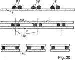
図20は、オプトエレクトロニクスウエハーと光学ウエハーとを相互に結合する、いくらか異なるアプローチを示す。まず、光学構造(図20には示されない)は光学ウエハー11上に複製される。そして、図の上部パネルに示されるように、スペーサ素子151が、光学ウエハーもしくはオプトエレクトロニクスウエハーのどちらかに加えられる。図中、スペーサ素子151は光学ウエハー上に加えられる。このことは、印刷プロセスで(整列された方法で)、もしくはスペーサ複製ツールを用いるプロセスで、なされることができる。スペーサはたとえば、作成されるデバイスの端の近くにあるように配置される;デバイスを囲んでもよい。印刷もしくは同様のプロセスの後、図20の断面形状に示唆されるように、スペーサ素子はまだ柔らかい。次の段階として、他のウエハー(図示される実施形態において、オプトエレクトロニクスウエハー1)が整列された方法で加えられる。このことは図の中部パネルに表される。硬化プロセスの間、スペーサ間の距離は、たとえばウエハーの端に配置される、適切な間隔制御手段によって制御される。そこで、スペーサ素子は硬化される。最後に、作成されるデバイスが、たとえばダイシング線152に沿ったダイシングにより、分離される。結果として得られるデバイスが、図20の下部パネルに示される。
FIG. 20 shows a somewhat different approach for bonding optoelectronic and optical wafers together. First, the optical structure (not shown in FIG. 20) is replicated on the
ここに説明される本実施形態および他の実施形態におけるダイシングプロセスは、従来のワンカットダイシングプロセスであろう。別の方法として、これは第1の段階(「プレダイシング」段階)を含む2段階の手順であり、ウエハーアセンブリが広い鋸歯を用いて事前にカットされる。この第1の段階において、複製物質のみが除去され、一方、基板は鋸でひかれるだけである。第2の段階で、基板は切断される。この2段階の手順は、結果として得られる製品の縁に追加のステッピングを残す。 The dicing process in this and other embodiments described herein will be a conventional one-cut dicing process. Alternatively, this is a two-stage procedure that includes a first stage (“pre-dicing” stage), in which the wafer assembly is pre-cut using a wide saw blade. In this first stage, only replication material is removed, while the substrate is only sawed. In the second stage, the substrate is cut. This two-step procedure leaves additional stepping at the edges of the resulting product.
スペーサ素子は任意の硬化可能なもしくはその他の固まる物質、たとえば紫外線硬化エポキシから作られるであろう。これらは透明である必要がなく、したがって、スペーサ物質は多様な物質から選択されるであろう。 The spacer element may be made from any curable or other solidifying material, such as UV curable epoxy. They do not need to be transparent and therefore the spacer material will be selected from a variety of materials.
代替的なアプローチは、エンボス加工された(マイクロ)光学構造を有するエンボス加工可能な物質の層を、オプトエレクトロニクスウエハー上に直接、もしくはオプトエレクトロニクスウエハー上の透明な中間層上に、提供することである。その時、非伝導物質の接触しない領域を保持することは、注意深く考慮されなければならない。 An alternative approach is to provide a layer of embossable material with an embossed (micro) optical structure directly on the optoelectronic wafer or on a transparent intermediate layer on the optoelectronic wafer. is there. At that time, maintaining non-contact areas of non-conductive material must be carefully considered.
図2および図3は、いくつかの光学能動領域2と、光学能動領域から間隔を取ったボンディングパッド23とから構成される、オプトエレクトロニクスデバイス21(ここではセンサーダイ、すなわち、ハウジングのない半導体デバイス)を示す。この実施例において、能動領域のアレイを有する光学センサーが示されるが、少なくとも1つの光学能動領域(部品)を有する任意のその他の種類のデバイスもまた含まれる。電気接触のためのこれらの領域は、この場合、光学能動領域のアレイ側にある;デバイスのレイアウトによって、これらはまた、任意の方法で配置されることができる、たとえば、各オプトエレクトロニクス部品に近接したボンディング領域である。受動的な光学部品の実施例であるマイクロレンズ24は、光学能動領域の上面に直接配置されることで、これに割り当てられる。図示された実施例において、マイクロ光学構造は、各光学能動領域に別々に提供されるが、1つの構造がいくつかの能動領域の光を集めることもまた可能であろう。さらに、図
示された実施例において、エンボス加工可能な物質の層は、デバイス全体にわたって連続的である。しかし、原則として、これはまた、マイクロ光学構造の間で遮断されることもあるだろう。
2 and 3 show an optoelectronic device 21 (here a sensor die, i.e. a semiconductor device without a housing), consisting of several optically
オプトエレクトロニクスデバイス21は、図4に示されるように、複数のオプトエレクトロニクスデバイスを含むウエハー1から作られる。
The
図2から図4より、(受動)光学部品もしくはシステムを、それらが局所的に大変明確に規定され、とりわけ、デバイスに電気接触する(たとえば結合により)要件に干渉しないような方法で提供することが、しばしば必要であることが明らかとなる。この局所的な限定がウエハーレベルで達成できることが望ましい。 2 to 4 provide (passive) optical components or systems in such a way that they are very well defined locally and in particular do not interfere with the requirements for electrical contact (eg by coupling) to the device. However, it becomes clear that it is often necessary. It is desirable that this local limitation can be achieved at the wafer level.
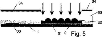
図5は受動光学部品の限定を確保するプロセスの第1の実施例を表す。電気接触領域は「写真構造の」複製プロセスによって複製物質から離される。このプロセスにより、たとえば紫外線などの放射によって硬化可能な、変形可能な物質31が、オプトエレクトロニクスウエハー1上に提供される。そこで、所望の構造32が、たとえばエンボス加工によって、物質に複製される。そのために用いられる複製ツール33は、受動光学部品の光学構造が光学能動領域に個別に設計される場合、オプトエレクトロニクスウエハーに整列される必要があるであろう。複製ツール33(その時、硬化放射のため透明である)もしくは光学パスのどこかに提供されるマスク34は、光学素子によって覆われる唯一の領域の照明を提供する。硬化しない物質は、硬化プロセスの後、洗い流されるか、もしくは成長する。
FIG. 5 represents a first embodiment of a process for ensuring the limitation of passive optical components. The electrical contact area is separated from the replication material by a “photographic structure” replication process. This process provides a
代替的な方法が図6および図7に描かれる。複製の局所的な限定は、空洞状の構造に複製することにより達成される。変形可能な、硬化可能な複製物質31が、光学能動領域に施される。光学マイクロ構造は液体物質内にエンボス加工される。複製ツール33は溝状の形状を含み、その中に(マイクロ光学)構造が配置される。したがってこれは、複製段階中に空洞41を形成し、空洞壁構造42を避ける必要のあるオプトエレクトロニクスウエハーの領域を密封するような方法で形成される。空洞内の複製物質は硬化される。空洞41の形状は、施された液体の量が光学素子に必要とされるボリュームと完全に一致しない場合に起こりうる気泡もしくはその他の影響の形成を防ぐべく、特別なボリュームを含むことができる。これらの追加的ボリューム(リザーバ)は、ウエハー平面の上にあってもよく、ウエハー平面から垂直方向に間隔を取ってもよい。ボリュームは、射出成形のようなプロセス段階において、図7に示されるように、硬化しない物質を空洞に注ぎ込むことにも用いられるチャネル43内に、配置されるか、接続されるかすることができる。
An alternative method is depicted in FIGS. Local limitation of replication is achieved by replicating into a hollow structure. A deformable,
図8は、さらに他の可能性を示す:(マイクロ)光学素子が、複製ツール42の空洞43に複製物質を施し、硬化されることで作成される。硬化された素子は、整列糊付けプロセスなどの、整列結合プロセスにより、オプトエレクトロニクスウエハーに取り付けられる。この可能性は、図8に示される実施形態と組み合わされるであろう。代替的なプロセスによると、オプトエレクトロニクスウエハーと複製ツールが、まず整列される。そして、複製物質が複製ツールの溝状の形状に施される。次に、複製ツール−まだ整列されている−はオプトエレクトロニクスウエハーに接触させられる。最後に、複製物質が硬化される。
FIG. 8 shows yet another possibility: (micro) optical elements are made by applying replication material to the
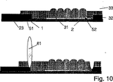
図9および図10は、局所的に限定された複製の、さらに他の異なる原則を示す。第1の段階で、いかなる非伝導物質からも離される必要のある領域は、保護層51で覆われる。保護層は、たとえば電気的に接触されなければならないために、非伝導物質から離される必要のある、全ての領域を保護する。これは、能動光学部品を構成する溝52のアレイを形成する格子状構造を有するであろう。代替的な方法として、保護層は、保護される領
域を覆う複数のばらばらの部分、もしくは、接触領域の保護を確保する任意のその他の形状を含むであろう。このことは、保護層が、非伝導物質から離される必要のある全ての領域を覆うことを、必ずしも包含するわけではない。たとえば、これが格子の形状を有する場合−能動光学部品を含む溝を形成する−これは必ずしも接触領域を覆う必要はない。これは複製物質が個々の溝に施される場合である(以下参照)。
9 and 10 show yet another different principle of locally confined replication. In the first stage, areas that need to be separated from any non-conductive material are covered with a
次の複製段階において、保護層は、マスクの一種として機能する。保護層は、たとえば、技術的に既知の方法で構成されたある種のレジストであろう。 In the next replication stage, the protective layer functions as a kind of mask. The protective layer may be, for example, some type of resist constructed in a manner known in the art.
もし保護層が溝52のアレイを形成するならば−たとえば言及された欧州特許出願第03 405 888号に示されるように−、マイクロ光学素子は溝の中に複製される。そこで、複製物質は溝内に局所的に施されるのが好ましいが、これは必須ではない。所望の構造が、液体もしくは塑性変形可能な複製物質に、複製ツール33を用いてエンボス加工される;たとえば、同時に多数のアレイ素子に関して。このために、複製ツールおよびその下にあるオプトエレクトロニクス部品は通常、整列される必要がある。そして、硬化段階がそれに続く。これは1度に1つの空洞/溝もしくは小数の空洞/溝に関してであってよい。そこで、たとえば、複製が各溝もしくは小数の溝に関して個々に達成され、複製段階に直接、硬化段階が続く。これはたとえば同じ複製ツールを用いて、さらなる空洞/溝に関して繰り返される。しばしば好適な、別の方法として、複製および硬化は、一度に全てのウエハーもしくは大部分の空洞/溝に関して行われる。
If the protective layer forms an array of grooves 52-as shown, for example, in the referenced European patent application 03 405 888-the micro-optics are replicated in the grooves. Thus, it is preferred that the replication material be applied locally in the groove, but this is not essential. The desired structure is embossed into a liquid or plastically deformable replication material using
硬化の後、電気接触領域上の保護層51は、−もしこれがレジスト物質から作られていれば−一般的に溶解されることで洗い流される。図9の下部パネルは、−空洞/溝に個々に施されたとしても−いかに複製物質が犠牲層の端から溢れ出る恐れがあるかを示す。このことは、光学能動領域/部品上のマイクロ光学機器の高さhの精度に影響しうる(図3参照)。ある特定の状況下では、このことはまた、犠牲層の溶解における問題、およびマイクロ光学素子の形状の不明確な定義を、もたらしうる。このことは、図10に示されるように、硬化の後で、かつ溶解段階の前のダイシングプロセスにより避けることができる。図10の上部パネルは、エンボス加工の間、複製物質56が犠牲層51の端から溢れ出る状態を示す。下部パネルには、ダイシングツール61が象徴的に示される。実際には、ダイシングは、ウエハーソーやパンチカッターなどの機械ツールによって、もしくはレーザーカッティングなどによって、なされることができる。犠牲層が果たすさらなる機能は、ダイシング/カッティングプロセスにおける、その下のウエハーの保護である。
After curing, the
光学機能に関しては、多くの実施形態において、正しい3D整列が重要である。横方向の精度(すなわち、x方向およびy方向への精度)が複製プロセスの整列によって管理されるのに対し、正確なz位置を確保する他の手段がある:光学能動領域の上の光学機器の高さhの正確な制御は、図11、図12および図13に表されるような特別な予防策を必要とするであろう。図11は、厚さに関して特別な予防策のない実施形態を示す。厚さhが重要である場合、犠牲層の厚さの正確な制御が要求される。いくつかの用途に関して10から20μmの正確さが十分である一方、厳しい用途に関して2μmもしくは1μmまでもが要求されうる。一般的な高さhは5μmから100μmの間であるが、数mmも要求されうる。hに関する実際の値および用いられる物質によっては、要求される精度は図11のアプローチでは実現することが難しい。適切なプロセスおよびパラメータもしくは代替の物質を見つけることはとても困難であろう。また、複製ツールと犠牲層との間の複製物質の溢れは、さらなる不確実さを引き起こしうる(図9の下部パネルに図示されるように)。 With respect to optical function, in many embodiments, correct 3D alignment is important. While lateral accuracy (ie accuracy in the x and y directions) is governed by the alignment of the replication process, there are other means of ensuring an accurate z position: optical instruments over the optical active area Accurate control of the height h will require special precautions as represented in FIGS. 11, 12 and 13. FIG. 11 shows an embodiment without any special precautions regarding thickness. If the thickness h is important, precise control of the sacrificial layer thickness is required. While accuracy of 10 to 20 μm is sufficient for some applications, up to 2 μm or even 1 μm may be required for demanding applications. Typical heights h are between 5 μm and 100 μm, but several mm may be required. Depending on the actual value for h and the materials used, the required accuracy is difficult to achieve with the approach of FIG. Finding the right process and parameters or alternative materials would be very difficult. Also, overflow of replication material between the replication tool and the sacrificial layer can cause further uncertainty (as illustrated in the lower panel of FIG. 9).
これらの問題は、図12および図13に示されるアプローチ、もしくは説明される原理の任意の組み合わせにより解決できる。第1の段階として、犠牲層は、正確で再現可能な
厚さをもたらすプロセスによって作成される。光学システム設計により必要とされる値からのいかなるずれも、くぼみ71もしくは空洞を複製ツール33の中に形成することにより補償されることができる。この文脈においての「くぼみ」は、複製ツール上の範囲であり、複製される構造は複製ツール33の表面73に対して、一定の明確に規定された距離だけずれる。このようにして、犠牲層の厚さと比較して強化された高さhは、図13に示されるように、当接突起72を構成する犠牲層51によって実現されるであろう。これらの当接突起は、溝の周囲に配置されると、上記で「溢れ」と説明された影響もまた防止する。ツールの作成における技術は、マイクロ機械加工および高精度構造と同様である、すなわち、くぼみの深さの大変良好な制御が保証されることができる。
These problems can be solved by the approach shown in FIGS. 12 and 13, or any combination of the principles described. As a first step, the sacrificial layer is created by a process that provides an accurate and reproducible thickness. Any deviation from the value required by the optical system design can be compensated by forming a
このことは機械設備においてのみ行われる必要があるので、最終的な精度に達するためにより高価な技術を用いることができる。このことは、それにより、複製側では高精度をもたらす標準的なプロセスが用いられ、一方機械設備側では必要とされる「端数の」値に達するために高価で大変正確なプロセスが用いられるであろうという、一般的な原則にしたがう。 Since this only needs to be done at the machine facility, more expensive techniques can be used to reach the final accuracy. This means that a standard process that provides high accuracy is used on the replication side, while an expensive and very accurate process is used on the machine side to reach the required "fractional" value. Follow the general principle of being.
犠牲層を用いることの主要な利点は、これらが、複製されたマイクロ光学素子のより複雑な形および形状を生成するのにもまた用いられることができるという事実である。ある可能性は、薄い犠牲層部分も、能動領域の上に適用することである。成長プロセスによりそれを硬化し、除去した後に、橋状の構造が形成されることができる。ある実施例が図14に示される。犠牲層部分81は能動部品2の上に配置され、これはここではたとえばレーザー構造(すなわち、たとえばVCSEL)である。この犠牲層部分を除去した後、空隙を構成する橋構造が形成される。このような空隙は、ある能動光学デバイスによって必要とされるであろう。
A major advantage of using sacrificial layers is the fact that they can also be used to generate more complex shapes and shapes of replicated micro-optics. One possibility is that a thin sacrificial layer portion is also applied over the active area. After it is cured and removed by a growth process, a bridge-like structure can be formed. One embodiment is shown in FIG. The
上記に説明された実施例は、硬化可能な複製物質を、ウエハー上もしくはウエハー上の選択されたスポット上に施すことを含む。このような硬化可能な複製物質は、たとえば、紫外線硬化エポキシまたは熱処理により硬化可能なポリマーである。しかし、このアプローチには選択肢がある。第1の選択肢は、熱可塑性物質、すなわち、高温で塑性変形可能な物質におけるホットエンボス加工である。第2の選択肢は、塑性変形可能な層をウエハー上に直接積層することである。構造は直接ウエハーに積層されるであろう。それに続く硬化もしくは冷却段階において、層は固まるであろう。積層のかわりに、塑性変形可能な層はウエハーに糊づけされてもよい。 The embodiments described above include applying a curable replication material on a wafer or selected spots on a wafer. Such curable replicating materials are, for example, UV curable epoxies or polymers curable by heat treatment. However, there are options for this approach. The first option is hot embossing in thermoplastic materials, ie materials that can be plastically deformed at high temperatures. The second option is to deposit a plastically deformable layer directly on the wafer. The structure will be laminated directly to the wafer. In subsequent curing or cooling steps, the layer will solidify. Instead of laminating, the plastically deformable layer may be glued to the wafer.
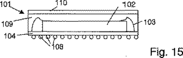
本発明のさらなる原則が図15を参照して説明される。最先端の技術によると、インターポーザーに結合された能動光学ダイの透明物質への封入は、とりわけ、それに続くIRリフロー段階などの加熱段階を含む用途に関して、実現可能ではなかった。このことの理由は、結合されたダイの上に成型され、結合を壊すことなく固められる既知の透明物質がないことである。 A further principle of the present invention is explained with reference to FIG. According to state-of-the-art technology, encapsulating an active optical die coupled to an interposer in a transparent material has not been feasible, especially for applications involving a heating step such as a subsequent IR reflow step. The reason for this is that there are no known transparent materials that are molded onto the bonded dies and set without breaking the bond.
図15を参照して説明される発明の態様は、半導体部品/デバイスは2層システムによって封入されるであろうという見識に基づく。最も外側の保護層の下のボリューム内の物質は、環境試験との互換性、オプトエレクトロニクス製造プロセス(たとえばIRリフロー)、および光学透明性および品質のように、ある要求される特性を有する必要がある。基本的な原則は、第1の層が、一定の距離を作成し(たとえば、ボンディングワイヤを覆い、保護するのに、または光学機器を正しいz位置に配置するのに十分なだけ厚い)、機械的パラメータ(この場合:機械的ストレスを低減するため、低いEモジュールを有する)を確保する機能を有することである。「ボリューム」層にあるのに適していると証明された物質区分は、低い弾性モジュールと高い光学透明性を有する物質である。これは、この物質の高いボリュームが、高く早い温度変化を含む環境条件にさらされるからである。
薄いもしくは柔軟性のある基板の上での厚い層の曲がりを防止するために、2つの選択肢がある。
The inventive aspects described with reference to FIG. 15 are based on the insight that semiconductor components / devices will be encapsulated by a two-layer system. The material in the volume under the outermost protective layer must have certain required properties, such as compatibility with environmental tests, optoelectronic manufacturing processes (eg IR reflow), and optical transparency and quality is there. The basic principle is that the first layer creates a certain distance (eg, thick enough to cover and protect the bonding wire, or to place the optics in the correct z position) A function to ensure a dynamic parameter (in this case: having a low E module to reduce mechanical stress). Material categories that have proven suitable for being in the “volume” layer are materials that have a low elastic module and high optical transparency. This is because the high volume of this material is exposed to environmental conditions including high and rapid temperature changes.
There are two options for preventing thick layer bending on thin or flexible substrates.
(i) 基板および最も外側の保護層と同じ熱膨張係数(CTE)を有する物質を用いる。このことは一般的に、プラスチック(上面)および半導体(底面)では不可能である。 (I) A material having the same coefficient of thermal expansion (CTE) as the substrate and the outermost protective layer is used. This is generally not possible with plastic (top) and semiconductor (bottom).
(ii) 大変低いEモジュール(すなわち、低膨張)を有する物質を用いる
PDMSはこのような物質の実施例である。PDMSはまた、高い光学透明性、環境試験条件に対する高い抵抗などの、さらなる要件を果たす(低いEモジュールとは別に)。
(Ii) Using a material with a very low E module (ie, low expansion) PDMS is an example of such a material. PDMS also fulfills additional requirements such as high optical transparency, high resistance to environmental test conditions (apart from the low E module).
しかし、最も外側の層が、硬さや引っかき抵抗などのさらなる物理的特性を有してさえいれば十分である。最も上の層は、透明性や、IRリフローなどのプロセスとの互換性とは別に、複製などのマイクロ構造技術と互換性があることもまた必要であり、保護(高湿度、極端な温度での硬い 「シールド」)を提供する必要がある。 However, it is sufficient that the outermost layer has additional physical properties such as hardness and scratch resistance. Apart from transparency and compatibility with processes such as IR reflow, the top layer also needs to be compatible with microstructural technologies such as replication and protection (at high humidity, extreme temperatures). Need to provide a hard “shield”).
図15は、チップ101内の、結合103により接触されたダイ102の封入を示す。ダイ102は、相互接続基板もしくはプリント基板(図示されない)を接触するために、後側にはんだバンプ108(ボールグリッドアレイ、BGA)のアレイを含むインターポーザー104の上に配置される。透明の物質は能動光学透明保護物質上に直接配置され、PDMS層109と、PDMS層の上の薄い最も外側のエポキシ層110との2つの層を含む。
FIG. 15 shows the encapsulation of the die 102 in contact with the
図16は、オプトエレクトロニクスチップの製造中の、半仕上げの製品のある実施例を示す。半仕上げの製品は、結合によって接続され、PDMSなどの透明物質の第1の層によって全体的に封入された複数のオプトエレクトロニクスダイ102を有する、広域(「ウエハースケール」)のインターポーザー104を含む。透明物質の第1の層は、硬化可能なエポキシなどの、透明物質の第2の層110によって覆われる。透明物質の第2の層は、複製機械構造、すなわち、オプトエレクトロニクスダイの場所における刻み目112を含む。刻み目は、入射光または出射光のために提供された場所において、チップ表面を引っかきから保護する。
FIG. 16 shows an example of a semi-finished product during the manufacture of an optoelectronic chip. The semi-finished product includes a wide area (“wafer scale”)
最終的なチップを製造するために、半仕上げの製品は個々のダイの間でばらばらにされ−図中の破線で示されるように−分離してパッケージ化されたチップを残す。 In order to produce the final chip, the semi-finished product is broken apart between the individual dies—as indicated by the dashed lines in the figure—to leave separate packaged chips.
本発明の原則は、パッケージ化されるオプトエレクトロニクスダイを含む技術的に既知であるさらなる構成、およびフリップチップ接触ダイを含むオプトエレクトロニクス機能性のないダイにもまた用いられるであろう。 The principles of the present invention may also be used for further configurations known in the art, including packaged optoelectronic dies, and dies without optoelectronic functionality, including flip chip contact dies.
能動デバイスを透明の2層システムに封入することの原則は、好ましくはウエハーレベルで、もしくは複数のダイを含む広領域のインターポーザー上で、能動光学部品と受動光学部品との直接的な組み合わせの原則と、組み合わされることができる。 The principle of encapsulating active devices in a transparent two-layer system is the direct combination of active and passive optical components, preferably at the wafer level or on a large area interposer containing multiple dies. Can be combined with the principle.
とりわけ、図2から図14を参照して説明されるアプローチは、オプトエレクトロニクスウエハーもしくは部品とレンズ機能との距離が、50より上から100μmの領域に入る時、その限界に達することができる。上述のプロセスは原則としてやはり実現可能であるが、複製物質の大変厚い層は固まるまで(たとえば紫外線硬化によって)に多くの時間を消費しうる。硬化中の収縮効果は、垂直方向におけるレンズの不正確な位置決めを招きかねない。ウエハースケールで、これらの影響はオプトエレクトロニクスウエハーの曲がりや欠けをも招きかねない。この潜在的な問題は、オプトエレクトロニクスウエハーと光
学表面との間の全ての物質が複製物質である必要はないという事実により、解決されることができる。そうではなく2層システムのうち1番上の層のみが複製プロセスと互換性のある特性を有する必要がある。
In particular, the approach described with reference to FIGS. 2 to 14 can reach its limit when the distance between the optoelectronic wafer or component and the lens function enters the region above 50 from 100 μm. The process described above is still feasible in principle, but a very thick layer of replication material can consume a lot of time until it hardens (eg by UV curing). The shrinkage effect during curing can lead to inaccurate positioning of the lens in the vertical direction. At the wafer scale, these effects can lead to bending or chipping of the optoelectronic wafer. This potential problem can be solved by the fact that not all material between the optoelectronic wafer and the optical surface need be a replicating material. Rather, only the top layer of a two-layer system needs to have characteristics compatible with the replication process.
発明にしたがった実施形態が図17に示される。複数の能動光学部品2から構成されるオプトエレクトロニクスウエハー1には、能動光学部品を封入するPDMS層121が備えられる。PDMS層121の上には、たとえば紫外線硬化エポキシである、複製物質の層122が配置される。複製層は、(受動)光学機能性を実装する複製構造123を含む。構造は光学能動部品に割り当てられ、たとえば、それらに整列される。
An embodiment according to the invention is shown in FIG. An
「低Eモジュール物質」の上に、その上に複製層を有する他の光学ウエハーがあってもよい。一実施例として、ガラスはPDMSに対して優れた接着性がある。より一般的には、複製は、PDMS層に塗布された層に直接であるよう限定されず、第2の層−複製構造を含む−が追加される前に行われるかも知れない。 There may be other optical wafers on top of the “low E module material” having a replication layer thereon. As an example, glass has excellent adhesion to PDMS. More generally, replication is not limited to being directly on the layer applied to the PDMS layer, but may occur before the second layer—including the replication structure—is added.
さらに他の方法として、PDMS層もまた構成されてよい。たとえば、複製が局所的に限定される空洞を作ることができる。この原則は図18に示される。空洞131はPDMS層109の中に、薄い最も外側の層110がマイクロ光学構造を備えられる位置に、備えられる。最も外側の層は、空洞が満たされ、たとえば均一の表面が提供されるような方法で提供される。このことは、空洞の位置を除いて、最も外側の層が本当に大変薄いことを可能にする。最も外側の物質は大変硬い物質であることが好ましく、切ることが容易でないため、このようにして、個々のデバイスをダイシングにより次に分離する段階が容易にされる。
As yet another method, a PDMS layer may also be constructed. For example, cavities can be created where replication is limited locally. This principle is illustrated in FIG. A
さらに他の代替的な「ウエハースケール」の封入と、オプトエレクトロニクスと光学機能性との組み合わせは、図19に示される。この実施形態において、薄い最も外側の層は、ウエハースケールでPDMS層109を完全には覆わないが、光学機能性および保護が所望される位置に対応するスポットに限定され、製品は最も外側の層の物質からは、ダイシングラインに沿った位置で離れている。たとえば紫外線硬化エポキシの、一致したスポット141は、たとえばスペーサ部分142をその端に沿って、マイクロ光学構造の機械的保護のために備えてもよい。スペーサ部分と同じくスポット141への層の限定は、複製ツールにおいて提供される一致した形状により、マイクロ光学構造を複製する段階において提供されるであろう。
Yet another alternative “wafer scale” encapsulation and the combination of optoelectronics and optical functionality is shown in FIG. In this embodiment, the thin outermost layer does not completely cover the
それぞれ図18および図19の第1および第2の層の特別な構造的形状が「ウエハースケール」のインターポーザーを参照して説明される一方、これらは図17を参照して、すなわちオプトエレクトロニクスウエハーに関連して、説明される本発明の実施形態にも存在するであろう。 While the specific structural shapes of the first and second layers of FIGS. 18 and 19, respectively, will be described with reference to a “wafer scale” interposer, these will be described with reference to FIG. 17, ie, an optoelectronic wafer. Will also be present in the embodiments of the invention described.
少なくとも1つのオプトエレクトロニクスデバイスを含むパッケージを製造する方法は、第1の透明物質の層の成型、硬化、場合によっては、異なるもしくは同一の物質のより多くの層のため、成型と硬化の段階の繰り返しを含むであろう。第1の透明物質の層における潜在的な空洞は、適宜構造化されたツールを硬化の間に適用することで、提供される。そこで、最も外側の層の物質が提供され、場合によっては光学構造が最も外側の層に複製される。この複製段階の間、最も外側の層のさらなる構造化、たとえば最も外側の層の不連続のスポットへの限定および/もしくはスペーサ部分の提供もまた、達成される。次に、最も外側の層は、複製ツールの除去の前に、硬化され/固められる。最後に、「ウエハースケール」のプロセスの場合、パッケージは個々のオプトエレクトロニクスデバイスに分離されるであろう。 A method of manufacturing a package that includes at least one optoelectronic device includes molding and curing a layer of a first transparent material, and in some cases, a molding and curing stage due to more layers of different or identical materials. Will include repetition. Potential cavities in the first layer of transparent material are provided by applying an appropriately structured tool during curing. There, the outermost layer material is provided, and in some cases the optical structure is replicated in the outermost layer. During this replication phase, further structuring of the outermost layer, for example limitation to discontinuous spots in the outermost layer and / or provision of spacer portions, is also achieved. The outermost layer is then cured / hardened prior to removal of the replication tool. Finally, in the case of a “wafer scale” process, the package will be separated into individual optoelectronic devices.
この成型アプローチは、機械に影響を受けるボンディングワイヤが損傷を受けないという利点を有する。他の方法として、1以上の層が糊付もしくは積層によって固定されるであろう。 This molding approach has the advantage that the bonding wire affected by the machine is not damaged. Alternatively, one or more layers may be secured by gluing or lamination.
上記に説明された本発明の実施形態とは別に、多様なその他の実施形態が存在する。たとえば、図15から図19を参照して説明された原則は、受動光学素子のみを含む光学システムの実施形態にもまた用いることができる。 Apart from the embodiments of the invention described above, there are a variety of other embodiments. For example, the principles described with reference to FIGS. 15-19 can also be used in embodiments of optical systems that include only passive optical elements.
Claims (12)
前記光学能動表面によって放射される電磁放射、および/もしくは、前記光学能動表面に衝突する電磁放射に影響を与えるよう機能する前記光学能動光学部品に配置された光学構造(12,13,123)を提供するステップを備える集積光学システムを製造する方法であり、前記光学構造は、
保護層(51)を前記ウエハーに加え、前記保護層は前記ウエハーの表面を部分的に覆うことと、
液体もしくは塑性変形可能な状態で、透明な物質を少なくとも前記能動光学部品のいくつかに配置することと、
複製ツール(33)によって、整列された方法で、前記透明な物質の表面に前記光学構造をエンボス加工することによって複製することで、複製プロセスにおいて複製ツールは保護層(51)もしくはその突起(72)に当接することと、
保護層(51)を除去することによって提供されることを特徴とし、
前記透明な物質を配置することは、前記光学構造をエンボス加工することによって複製する前に実行され、
前記方法はさらに、前記光学構造を有する半導体ウエハーを少なくとも1つの能動光学部品および少なくとも1つの光学構造を含む部分に分離するステップを含む、集積光学システムを製造する方法。Providing a wafer (1) having an active optical component (2), each active optical component comprising a step having an optical active surface, wherein electromagnetic radiation is emitted by the optical active surface, and / or Electromagnetic radiation impinges on the optically active surface;
An optical structure (12, 13, 123) disposed on the optical active optical component that functions to affect electromagnetic radiation emitted by the optical active surface and / or electromagnetic radiation impinging on the optical active surface; A method of manufacturing an integrated optical system comprising the step of providing, the optical structure comprising:
Adding a protective layer (51) to the wafer, the protective layer partially covering the surface of the wafer;
Placing a transparent material in at least some of the active optical components in a liquid or plastically deformable state;
The replication tool (33), in an aligned manner, wherein by duplicating by embossing the optical structure on the surface of a transparent material, copy protection layer is replication tool in the process (51) or projections thereof (72 ), And
Characterized in that it is provided by removing the protective layer (51),
Placing the transparent material is performed prior to replication by embossing the optical structure;
The method further includes the step of separating a semiconductor wafer having the optical structure into at least one active optical component and a portion including at least one optical structure.
前記光学能動表面によって放射される電磁放射、および/もしくは、前記光学能動表面に衝突する電磁放射に影響を与えるよう機能する前記光学能動光学部品に配置された光学構造(12,13,123)を提供するステップを備える集積光学システムを製造する方法であり、前記光学構造は、
保護層(51)を前記ウエハーに加え、前記保護層は前記ウエハーの表面を部分的に覆うことと、
液体もしくは塑性変形可能な状態で、透明な物質を少なくとも前記能動光学部品のいくつかに配置することと、
複製ツール(33)によって、整列された方法で、前記透明な物質の表面に前記光学構造を複製することで、複製プロセスにおいて複製ツールは保護層(51)もしくはその突起(72)に当接することと、
保護層(51)を除去することによって提供されることを特徴とし、
前記方法はさらに、前記光学構造を有する半導体ウエハーを少なくとも1つの能動光学部品および少なくとも1つの光学構造を含む部分に分離するステップを含み、
前記透明な物質が、前記保護層のくぼみにより形成された溝に配置され、もしくは前記保護層を含む前記ウエハー上に広域にわたり配置され、
ダイシングステップが、硬化ステップの後に、前記保護層の除去前に行われ、前記ダイシングステップは、前記透明な物質の溝を、前記保護層に接する場所でカットすることを含むことを特徴とする、集積光学システムを製造する方法。Providing a wafer (1) having an active optical component (2), each active optical component comprising a step having an optical active surface, wherein electromagnetic radiation is emitted by the optical active surface, and / or Electromagnetic radiation impinges on the optically active surface;
An optical structure (12, 13, 123) disposed on the optical active optical component that functions to affect electromagnetic radiation emitted by the optical active surface and / or electromagnetic radiation impinging on the optical active surface; A method of manufacturing an integrated optical system comprising the step of providing, the optical structure comprising:
Adding a protective layer (51) to the wafer, the protective layer partially covering the surface of the wafer;
Placing a transparent material in at least some of the active optical components in a liquid or plastically deformable state;
By replicating the optical structure on the surface of the transparent material in an aligned manner by the replication tool (33), the replication tool abuts the protective layer (51) or its protrusion (72) in the replication process. When,
Characterized in that it is provided by removing the protective layer (51),
The method further includes separating a semiconductor wafer having the optical structure into at least one active optical component and a portion including at least one optical structure;
The transparent material is disposed in a groove formed by a recess of the protective layer, or is disposed over a wide area on the wafer including the protective layer;
A dicing step is performed after the curing step and before the removal of the protective layer, and the dicing step includes cutting the groove of the transparent material at a location in contact with the protective layer. A method of manufacturing an integrated optical system.
前記光学能動表面によって放射される電磁放射、および/もしくは、前記光学能動表面に衝突する電磁放射に影響を与えるよう機能する前記光学能動光学部品に配置された光学構造(12,13,123)を提供するステップを備える集積光学システムを製造する方法であり、前記光学構造は、
保護層(51)を前記ウエハーに加え、前記保護層は前記ウエハーの表面を部分的に覆うことと、
液体もしくは塑性変形可能な状態で、透明な物質を少なくとも前記能動光学部品のいくつかに配置することと、
複製ツール(33)によって、整列された方法で、前記透明な物質の表面に前記光学構造を複製することで、複製プロセスにおいて複製ツールは保護層(51)もしくはその突起(72)に当接することと、
保護層(51)を除去することによって提供されることを特徴とし、
前記方法はさらに、前記光学構造を有する半導体ウエハーを少なくとも1つの能動光学部品および少なくとも1つの光学構造を含む部分に分離するステップを含み、
前記透明な物質が、前記保護層のくぼみにより形成された溝に配置され、
前記保護層(51)は、溝の周囲に配置された当接突起(72)を含むことを特徴とする、集積光学システムを製造する方法。Providing a wafer (1) having an active optical component (2), each active optical component comprising a step having an optical active surface, wherein electromagnetic radiation is emitted by the optical active surface, and / or Electromagnetic radiation impinges on the optically active surface;
An optical structure (12, 13, 123) disposed on the optical active optical component that functions to affect electromagnetic radiation emitted by the optical active surface and / or electromagnetic radiation impinging on the optical active surface; A method of manufacturing an integrated optical system comprising the step of providing, the optical structure comprising:
Adding a protective layer (51) to the wafer, the protective layer partially covering the surface of the wafer;
Placing a transparent material in at least some of the active optical components in a liquid or plastically deformable state;
By replicating the optical structure on the surface of the transparent material in an aligned manner by the replication tool (33), the replication tool abuts the protective layer (51) or its protrusion (72) in the replication process. When,
Characterized in that it is provided by removing the protective layer (51),
The method further includes separating a semiconductor wafer having the optical structure into at least one active optical component and a portion including at least one optical structure;
The transparent material is disposed in a groove formed by a recess in the protective layer;
Method for manufacturing an integrated optical system, characterized in that the protective layer (51) comprises abutment protrusions (72) arranged around the groove.
Applications Claiming Priority (3)
| Application Number | Priority Date | Filing Date | Title |
|---|---|---|---|
| EP04405110A EP1569276A1 (en) | 2004-02-27 | 2004-02-27 | Micro-optics on optoelectronics |
| EP04405110.0 | 2004-02-27 | ||
| PCT/CH2005/000109 WO2005083789A2 (en) | 2004-02-27 | 2005-02-25 | Micro-optics on optoelectronics |
Publications (3)
| Publication Number | Publication Date |
|---|---|
| JP2007524243A JP2007524243A (en) | 2007-08-23 |
| JP2007524243A5 JP2007524243A5 (en) | 2008-03-27 |
| JP4903685B2 true JP4903685B2 (en) | 2012-03-28 |
Family
ID=34746192
Family Applications (1)
| Application Number | Title | Priority Date | Filing Date |
|---|---|---|---|
| JP2007500029A Active JP4903685B2 (en) | 2004-02-27 | 2005-02-25 | Method for manufacturing an integrated optical system |
Country Status (9)
| Country | Link |
|---|---|
| US (1) | US7457490B2 (en) |
| EP (2) | EP1569276A1 (en) |
| JP (1) | JP4903685B2 (en) |
| KR (1) | KR101194452B1 (en) |
| CN (1) | CN1947254B (en) |
| AT (1) | ATE498910T1 (en) |
| DE (1) | DE602005026367D1 (en) |
| TW (1) | TWI362058B (en) |
| WO (1) | WO2005083789A2 (en) |
Families Citing this family (48)
| Publication number | Priority date | Publication date | Assignee | Title |
|---|---|---|---|---|
| US6297548B1 (en) | 1998-06-30 | 2001-10-02 | Micron Technology, Inc. | Stackable ceramic FBGA for high thermal applications |
| WO2007060592A2 (en) * | 2005-11-22 | 2007-05-31 | Koninklijke Philips Electronics N.V. | Light emitting module and manufacturing method |
| JP2007258672A (en) * | 2006-02-22 | 2007-10-04 | Sharp Corp | Light-emitting diode and its manufacturing method |
| JP4765663B2 (en) * | 2006-02-23 | 2011-09-07 | パナソニック電工株式会社 | Infrared communication module manufacturing method |
| US7785915B2 (en) * | 2006-10-30 | 2010-08-31 | Aptina Imaging Corporation | Wafer level method of locating focal plane of imager devices |
| US20080181558A1 (en) * | 2007-01-31 | 2008-07-31 | Hartwell Peter G | Electronic and optical circuit integration through wafer bonding |
| US7754600B2 (en) | 2007-03-01 | 2010-07-13 | Hewlett-Packard Development Company, L.P. | Methods of forming nanostructures on metal-silicide crystallites, and resulting structures and devices |
| US20090032925A1 (en) * | 2007-07-31 | 2009-02-05 | England Luke G | Packaging with a connection structure |
| CN101784378A (en) | 2007-08-31 | 2010-07-21 | 柯尼卡美能达精密光学株式会社 | Molding method, optical element manufacturing method, and arrayed optical element |
| EP2060493B1 (en) * | 2007-11-13 | 2010-06-23 | Oy M. Haloila Ab | Film delivery device and use of same |
| TWI478808B (en) | 2007-12-19 | 2015-04-01 | Heptagon Micro Optics Pte Ltd | Manufacturing optical elements |
| TWI481496B (en) | 2007-12-19 | 2015-04-21 | Heptagon Micro Optics Pte Ltd | Manufacturing optical elements |
| SG142321A1 (en) | 2008-04-24 | 2009-11-26 | Micron Technology Inc | Pre-encapsulated cavity interposer |
| GB2460822A (en) * | 2008-06-03 | 2009-12-16 | Cambridge Display Tech Ltd | Organic electroluminescent device |
| US7920342B2 (en) * | 2008-07-01 | 2011-04-05 | Aptina Imaging Corporation | Over-molded glass lenses and method of forming the same |
| CN102077121B (en) | 2008-07-04 | 2013-10-23 | 柯尼卡美能达精密光学株式会社 | Imaging lens, and manufacturing method and imaging unit therefor |
| CN101364568B (en) * | 2008-07-10 | 2011-11-30 | 旭丽电子(广州)有限公司 | Camera module manufacturing method and camera module manufactured thereby |
| TWI419557B (en) * | 2008-07-11 | 2013-12-11 | Lite On Electronics Guangzhou | Camera module, method for manufacturing the same, and wafer structure formed with multiple camera modules |
| US8828174B2 (en) | 2008-08-20 | 2014-09-09 | Heptagon Micro Optics Pte. Ltd. | Method of manufacturing a plurality of optical devices |
| JP5715747B2 (en) * | 2008-09-30 | 2015-05-13 | セミコンダクター・コンポーネンツ・インダストリーズ・リミテッド・ライアビリティ・カンパニー | Circuit device and manufacturing method thereof |
| US20110187878A1 (en) * | 2010-02-02 | 2011-08-04 | Primesense Ltd. | Synchronization of projected illumination with rolling shutter of image sensor |
| WO2011156926A1 (en) | 2010-06-14 | 2011-12-22 | Heptagon Oy | Method of manufacturing a plurality of optical devices |
| SG191817A1 (en) | 2011-07-19 | 2013-08-30 | Heptagon Micro Optics Pte Ltd | Opto -electronic modules and methods of manufacturing the same |
| JP2014521992A (en) | 2011-07-19 | 2014-08-28 | ヘプタゴン・マイクロ・オプティクス・プライベート・リミテッド | Method for manufacturing passive optical component and device comprising passive optical component |
| CN103858230B (en) * | 2011-08-10 | 2018-03-27 | 新加坡恒立私人有限公司 | Optoelectronic module and the method for manufacturing the optoelectronic module |
| DE102011113483B4 (en) * | 2011-09-13 | 2023-10-19 | OSRAM Opto Semiconductors Gesellschaft mit beschränkter Haftung | Method for producing a plurality of optoelectronic components and optoelectronic component |
| WO2013049948A1 (en) * | 2011-10-06 | 2013-04-11 | Heptagon Micro Optics Pte. Ltd. | Method for wafer-level manufacturing of objects and corresponding semi-finished products |
| WO2013091829A1 (en) | 2011-12-22 | 2013-06-27 | Heptagon Micro Optics Pte. Ltd. | Opto-electronic modules, in particular flash modules, and method for manufacturing the same |
| US9329080B2 (en) | 2012-02-15 | 2016-05-03 | Aplle Inc. | Modular optics for scanning engine having beam combining optics with a prism intercepted by both beam axis and collection axis |
| US9651417B2 (en) | 2012-02-15 | 2017-05-16 | Apple Inc. | Scanning depth engine |
| WO2014012603A1 (en) | 2012-07-17 | 2014-01-23 | Heptagon Micro Optics Pte. Ltd. | Optical devices, in particular computational cameras, and methods for manufacturing the same |
| TWI707483B (en) | 2012-07-17 | 2020-10-11 | 新加坡商新加坡恒立私人有限公司 | Opto-electronic module for emitting light of variable intensity distribution |
| TW201417250A (en) * | 2012-07-17 | 2014-05-01 | 海特根微光學公司 | Optical module, in particular opto-electronic module, and method of manufacturing the same |
| TWM448798U (en) * | 2012-08-10 | 2013-03-11 | Meicer Semiconductor Inc | Optical device package module |
| DE102012109183A1 (en) * | 2012-09-27 | 2014-03-27 | Osram Opto Semiconductors Gmbh | Optoelectronic device |
| US8606057B1 (en) | 2012-11-02 | 2013-12-10 | Heptagon Micro Optics Pte. Ltd. | Opto-electronic modules including electrically conductive connections for integration with an electronic device |
| US10403671B2 (en) * | 2013-12-10 | 2019-09-03 | Ams Sensors Singapore Pte. Ltd. | Wafer-level optical modules and methods for manufacturing the same |
| US10018788B2 (en) | 2014-10-28 | 2018-07-10 | Hewlett Packard Enterprise Development Lp | Photonic interposer with wafer bonded microlenses |
| DE102014116134A1 (en) * | 2014-11-05 | 2016-05-12 | Osram Opto Semiconductors Gmbh | Method for producing an optoelectronic component and optoelectronic component |
| US10692912B2 (en) | 2015-01-06 | 2020-06-23 | Huf Hülsbeck & Fürst Gmbh & Co. Kg | Optical device for exposure of a sensor device for a vehicle |
| WO2017055160A1 (en) | 2015-10-01 | 2017-04-06 | Koninklijke Philips N.V. | Light emitting device |
| DE102016103123A1 (en) * | 2016-02-23 | 2017-08-24 | Vishay Semiconductor Gmbh | Optoelectronic device |
| TWI735562B (en) | 2016-04-08 | 2021-08-11 | 新加坡商新加坡恒立私人有限公司 | Thin optoelectronic modules with apertures and their manufacture |
| DE102017100997A1 (en) * | 2017-01-19 | 2018-07-19 | Osram Opto Semiconductors Gmbh | Semiconductor laser and method for producing such a semiconductor laser |
| KR20200103233A (en) * | 2019-02-22 | 2020-09-02 | 삼성디스플레이 주식회사 | Display apparatus and method for manufacturing the same |
| US20200402871A1 (en) * | 2019-06-24 | 2020-12-24 | Magic Leap, Inc. | Polymer patterned disk stack manufacturing |
| US10777611B1 (en) * | 2019-09-27 | 2020-09-15 | Sony Semiconductor Solutions Corporation | Image sensor |
| US11747555B2 (en) | 2021-10-04 | 2023-09-05 | Eagle Technology, Llc | Optical assembly having commonly-shaped optical modules and associated methods |
Citations (5)
| Publication number | Priority date | Publication date | Assignee | Title |
|---|---|---|---|---|
| JPS56103483A (en) * | 1980-01-21 | 1981-08-18 | Fuji Photo Film Co Ltd | Manufacture of semiconductor device for photoelectric conversion |
| JPH07111343A (en) * | 1993-10-13 | 1995-04-25 | Matsushita Electron Corp | Photoelectric device |
| JPH11340480A (en) * | 1998-05-21 | 1999-12-10 | Tokai Rika Co Ltd | Plastic package |
| JP2000275405A (en) * | 1999-03-29 | 2000-10-06 | Canon Inc | Manufacture of microstructure array, manufacture of die for micro-lens array, and manufacture of micro-lens array with use thereof |
| JP2005039195A (en) * | 2003-06-26 | 2005-02-10 | Nippon Sheet Glass Co Ltd | Manufacturing method of light emitting element with built-in lens |
Family Cites Families (10)
| Publication number | Priority date | Publication date | Assignee | Title |
|---|---|---|---|---|
| US20020053742A1 (en) * | 1995-09-01 | 2002-05-09 | Fumio Hata | IC package and its assembly method |
| US6235141B1 (en) * | 1996-09-27 | 2001-05-22 | Digital Optics Corporation | Method of mass producing and packaging integrated optical subsystems |
| US6436265B1 (en) | 1999-03-29 | 2002-08-20 | Canon Kabushiki Kaisha | Microstructure array, and apparatus and method for forming the microstructure array, and a mold for fabricating a microstructure array |
| TW588414B (en) * | 2000-06-08 | 2004-05-21 | Toshiba Corp | Alignment method, overlap inspecting method and mask |
| US20040012698A1 (en) * | 2001-03-05 | 2004-01-22 | Yasuo Suda | Image pickup model and image pickup device |
| JP2002353763A (en) * | 2001-05-29 | 2002-12-06 | Mitsubishi Electric Corp | Manufacturing method for piezoelectric element device |
| JP4167443B2 (en) | 2002-01-30 | 2008-10-15 | 日本放送協会 | Solid-state image sensor |
| JP2004063751A (en) | 2002-07-29 | 2004-02-26 | Fuji Photo Film Co Ltd | Solid-state image sensing device and its manufacturing method |
| GB0213722D0 (en) * | 2002-06-14 | 2002-07-24 | Suisse Electronique Microtech | Micro electrical mechanical systems |
| US7414661B2 (en) * | 2002-08-13 | 2008-08-19 | Micron Technology, Inc. | CMOS image sensor using gradient index chip scale lenses |
-
2004
- 2004-02-27 EP EP04405110A patent/EP1569276A1/en not_active Withdrawn
-
2005
- 2005-02-24 TW TW094105676A patent/TWI362058B/en active
- 2005-02-25 KR KR1020067019870A patent/KR101194452B1/en active IP Right Grant
- 2005-02-25 CN CN2005800133746A patent/CN1947254B/en active Active
- 2005-02-25 EP EP05706528A patent/EP1719178B1/en active Active
- 2005-02-25 WO PCT/CH2005/000109 patent/WO2005083789A2/en active Application Filing
- 2005-02-25 AT AT05706528T patent/ATE498910T1/en not_active IP Right Cessation
- 2005-02-25 DE DE602005026367T patent/DE602005026367D1/en active Active
- 2005-02-25 JP JP2007500029A patent/JP4903685B2/en active Active
-
2006
- 2006-08-23 US US11/466,640 patent/US7457490B2/en active Active
Patent Citations (5)
| Publication number | Priority date | Publication date | Assignee | Title |
|---|---|---|---|---|
| JPS56103483A (en) * | 1980-01-21 | 1981-08-18 | Fuji Photo Film Co Ltd | Manufacture of semiconductor device for photoelectric conversion |
| JPH07111343A (en) * | 1993-10-13 | 1995-04-25 | Matsushita Electron Corp | Photoelectric device |
| JPH11340480A (en) * | 1998-05-21 | 1999-12-10 | Tokai Rika Co Ltd | Plastic package |
| JP2000275405A (en) * | 1999-03-29 | 2000-10-06 | Canon Inc | Manufacture of microstructure array, manufacture of die for micro-lens array, and manufacture of micro-lens array with use thereof |
| JP2005039195A (en) * | 2003-06-26 | 2005-02-10 | Nippon Sheet Glass Co Ltd | Manufacturing method of light emitting element with built-in lens |
Also Published As
| Publication number | Publication date |
|---|---|
| TW200532761A (en) | 2005-10-01 |
| WO2005083789A3 (en) | 2006-05-11 |
| EP1719178A2 (en) | 2006-11-08 |
| KR20070004774A (en) | 2007-01-09 |
| TWI362058B (en) | 2012-04-11 |
| US20070009223A1 (en) | 2007-01-11 |
| KR101194452B1 (en) | 2012-10-24 |
| CN1947254B (en) | 2010-12-29 |
| DE602005026367D1 (en) | 2011-03-31 |
| US7457490B2 (en) | 2008-11-25 |
| ATE498910T1 (en) | 2011-03-15 |
| WO2005083789A2 (en) | 2005-09-09 |
| JP2007524243A (en) | 2007-08-23 |
| EP1569276A1 (en) | 2005-08-31 |
| CN1947254A (en) | 2007-04-11 |
| EP1719178B1 (en) | 2011-02-16 |
Similar Documents
| Publication | Publication Date | Title |
|---|---|---|
| JP4903685B2 (en) | Method for manufacturing an integrated optical system | |
| JP6763807B2 (en) | Manufacturing methods for passive optics and devices with passive optics | |
| US7535949B2 (en) | VCSEL with integrated lens | |
| JP6987907B2 (en) | Wafer-level methods for equipment, especially optics | |
| Bosman et al. | Ultrathin optoelectronic device packaging in flexible carriers | |
| TW201812379A (en) | Method for manufacturing optical devices and method for manufacturing a spacer wafer on an optics wafer | |
| TW201417250A (en) | Optical module, in particular opto-electronic module, and method of manufacturing the same | |
| TW201415648A (en) | Sensor module and method of manufacturing the same | |
| US7391576B2 (en) | Manufacturing of optical units for semiconductor packages with optical sensors | |
| JP4714499B2 (en) | Semiconductor imaging device and manufacturing method thereof | |
| EP1654572B1 (en) | A screen-printing method of encapsulating optoelectronic chips | |
| JP2005294444A (en) | Semiconductor device and its manufacturing method, mounting structure and mounting method thereof, dummy wafer and its manufacturing method | |
| WO2020122813A1 (en) | Vacuum injection molding for optoelectronic modules | |
| TW201415614A (en) | Compact optical module and method for manufacturing the same |
Legal Events
| Date | Code | Title | Description |
|---|---|---|---|
| A521 | Request for written amendment filed |
Free format text: JAPANESE INTERMEDIATE CODE: A523 Effective date: 20080206 |
|
| A621 | Written request for application examination |
Free format text: JAPANESE INTERMEDIATE CODE: A621 Effective date: 20080206 |
|
| A977 | Report on retrieval |
Free format text: JAPANESE INTERMEDIATE CODE: A971007 Effective date: 20110309 |
|
| A131 | Notification of reasons for refusal |
Free format text: JAPANESE INTERMEDIATE CODE: A131 Effective date: 20110315 |
|
| A601 | Written request for extension of time |
Free format text: JAPANESE INTERMEDIATE CODE: A601 Effective date: 20110614 |
|
| A602 | Written permission of extension of time |
Free format text: JAPANESE INTERMEDIATE CODE: A602 Effective date: 20110621 |
|
| A601 | Written request for extension of time |
Free format text: JAPANESE INTERMEDIATE CODE: A601 Effective date: 20110714 |
|
| A602 | Written permission of extension of time |
Free format text: JAPANESE INTERMEDIATE CODE: A602 Effective date: 20110722 |
|
| A521 | Request for written amendment filed |
Free format text: JAPANESE INTERMEDIATE CODE: A523 Effective date: 20110727 |
|
| A131 | Notification of reasons for refusal |
Free format text: JAPANESE INTERMEDIATE CODE: A131 Effective date: 20110920 |
|
| A521 | Request for written amendment filed |
Free format text: JAPANESE INTERMEDIATE CODE: A523 Effective date: 20111104 |
|
| TRDD | Decision of grant or rejection written | ||
| A01 | Written decision to grant a patent or to grant a registration (utility model) |
Free format text: JAPANESE INTERMEDIATE CODE: A01 Effective date: 20111213 |
|
| A01 | Written decision to grant a patent or to grant a registration (utility model) |
Free format text: JAPANESE INTERMEDIATE CODE: A01 |
|
| A61 | First payment of annual fees (during grant procedure) |
Free format text: JAPANESE INTERMEDIATE CODE: A61 Effective date: 20120105 |
|
| R150 | Certificate of patent or registration of utility model |
Ref document number: 4903685 Country of ref document: JP Free format text: JAPANESE INTERMEDIATE CODE: R150 Free format text: JAPANESE INTERMEDIATE CODE: R150 |
|
| FPAY | Renewal fee payment (event date is renewal date of database) |
Free format text: PAYMENT UNTIL: 20150113 Year of fee payment: 3 |
|
| S111 | Request for change of ownership or part of ownership |
Free format text: JAPANESE INTERMEDIATE CODE: R313113 |
|
| FPAY | Renewal fee payment (event date is renewal date of database) |
Free format text: PAYMENT UNTIL: 20150113 Year of fee payment: 3 |
|
| R350 | Written notification of registration of transfer |
Free format text: JAPANESE INTERMEDIATE CODE: R350 |
|
| R250 | Receipt of annual fees |
Free format text: JAPANESE INTERMEDIATE CODE: R250 |
|
| R250 | Receipt of annual fees |
Free format text: JAPANESE INTERMEDIATE CODE: R250 |
|
| R250 | Receipt of annual fees |
Free format text: JAPANESE INTERMEDIATE CODE: R250 |
|
| R250 | Receipt of annual fees |
Free format text: JAPANESE INTERMEDIATE CODE: R250 |
|
| R250 | Receipt of annual fees |
Free format text: JAPANESE INTERMEDIATE CODE: R250 |
|
| R250 | Receipt of annual fees |
Free format text: JAPANESE INTERMEDIATE CODE: R250 |
|
| R250 | Receipt of annual fees |
Free format text: JAPANESE INTERMEDIATE CODE: R250 |
|
| R250 | Receipt of annual fees |
Free format text: JAPANESE INTERMEDIATE CODE: R250 |
|
| R250 | Receipt of annual fees |
Free format text: JAPANESE INTERMEDIATE CODE: R250 |
|
| R250 | Receipt of annual fees |
Free format text: JAPANESE INTERMEDIATE CODE: R250 |