JP2014521992A - Method for manufacturing passive optical component and device comprising passive optical component - Google Patents
Method for manufacturing passive optical component and device comprising passive optical component Download PDFInfo
- Publication number
- JP2014521992A JP2014521992A JP2014520486A JP2014520486A JP2014521992A JP 2014521992 A JP2014521992 A JP 2014521992A JP 2014520486 A JP2014520486 A JP 2014520486A JP 2014520486 A JP2014520486 A JP 2014520486A JP 2014521992 A JP2014521992 A JP 2014521992A
- Authority
- JP
- Japan
- Prior art keywords
- transparent
- wafer
- optical
- passive optical
- optical component
- Prior art date
- Legal status (The legal status is an assumption and is not a legal conclusion. Google has not performed a legal analysis and makes no representation as to the accuracy of the status listed.)
- Pending
Links
- 230000003287 optical effect Effects 0.000 title claims abstract description 201
- 238000004519 manufacturing process Methods 0.000 title claims abstract description 57
- 238000000034 method Methods 0.000 title claims abstract description 46
- 239000000463 material Substances 0.000 claims abstract description 67
- 230000000903 blocking effect Effects 0.000 claims abstract description 41
- 239000012780 transparent material Substances 0.000 claims abstract description 32
- 230000003595 spectral effect Effects 0.000 claims abstract description 14
- 230000010076 replication Effects 0.000 claims description 31
- 230000005693 optoelectronics Effects 0.000 claims description 26
- 239000002243 precursor Substances 0.000 claims description 21
- 238000004891 communication Methods 0.000 claims description 2
- 235000012431 wafers Nutrition 0.000 description 161
- 239000011265 semifinished product Substances 0.000 description 22
- 239000000758 substrate Substances 0.000 description 13
- 125000006850 spacer group Chemical group 0.000 description 10
- 238000010586 diagram Methods 0.000 description 8
- 238000005498 polishing Methods 0.000 description 6
- 229920000642 polymer Polymers 0.000 description 6
- 238000000926 separation method Methods 0.000 description 6
- 238000001723 curing Methods 0.000 description 5
- 238000000465 moulding Methods 0.000 description 5
- 238000001514 detection method Methods 0.000 description 4
- 239000003822 epoxy resin Substances 0.000 description 4
- 238000005530 etching Methods 0.000 description 4
- 238000010438 heat treatment Methods 0.000 description 4
- 229920000647 polyepoxide Polymers 0.000 description 4
- 230000005855 radiation Effects 0.000 description 4
- 239000007787 solid Substances 0.000 description 4
- 230000015572 biosynthetic process Effects 0.000 description 3
- 238000005553 drilling Methods 0.000 description 3
- 238000004049 embossing Methods 0.000 description 3
- 239000007788 liquid Substances 0.000 description 3
- 230000005499 meniscus Effects 0.000 description 3
- -1 polydimethylsiloxane Polymers 0.000 description 3
- 239000002861 polymer material Substances 0.000 description 3
- 239000004065 semiconductor Substances 0.000 description 3
- 229910000679 solder Inorganic materials 0.000 description 3
- 229920001187 thermosetting polymer Polymers 0.000 description 3
- 150000001875 compounds Chemical class 0.000 description 2
- 239000000470 constituent Substances 0.000 description 2
- 230000005670 electromagnetic radiation Effects 0.000 description 2
- 239000011521 glass Substances 0.000 description 2
- 230000000149 penetrating effect Effects 0.000 description 2
- 230000003362 replicative effect Effects 0.000 description 2
- 238000007650 screen-printing Methods 0.000 description 2
- 238000001228 spectrum Methods 0.000 description 2
- 238000009736 wetting Methods 0.000 description 2
- 230000006399 behavior Effects 0.000 description 1
- 239000011248 coating agent Substances 0.000 description 1
- 238000000576 coating method Methods 0.000 description 1
- 239000002131 composite material Substances 0.000 description 1
- 238000005520 cutting process Methods 0.000 description 1
- 230000001419 dependent effect Effects 0.000 description 1
- 239000004205 dimethyl polysiloxane Substances 0.000 description 1
- LNEPOXFFQSENCJ-UHFFFAOYSA-N haloperidol Chemical compound C1CC(O)(C=2C=CC(Cl)=CC=2)CCN1CCCC(=O)C1=CC=C(F)C=C1 LNEPOXFFQSENCJ-UHFFFAOYSA-N 0.000 description 1
- 238000001746 injection moulding Methods 0.000 description 1
- 230000010354 integration Effects 0.000 description 1
- 238000005304 joining Methods 0.000 description 1
- 239000011344 liquid material Substances 0.000 description 1
- 239000002184 metal Substances 0.000 description 1
- 229910052751 metal Inorganic materials 0.000 description 1
- 150000002739 metals Chemical class 0.000 description 1
- 230000002093 peripheral effect Effects 0.000 description 1
- 229920000435 poly(dimethylsiloxane) Polymers 0.000 description 1
- 229920001296 polysiloxane Polymers 0.000 description 1
- 239000000047 product Substances 0.000 description 1
- 238000003847 radiation curing Methods 0.000 description 1
- 230000003746 surface roughness Effects 0.000 description 1
- 230000002123 temporal effect Effects 0.000 description 1
- 239000011345 viscous material Substances 0.000 description 1
Images


Classifications
-
- G—PHYSICS
- G02—OPTICS
- G02B—OPTICAL ELEMENTS, SYSTEMS OR APPARATUS
- G02B3/00—Simple or compound lenses
- G02B3/0006—Arrays
- G02B3/0012—Arrays characterised by the manufacturing method
- G02B3/0031—Replication or moulding, e.g. hot embossing, UV-casting, injection moulding
-
- B—PERFORMING OPERATIONS; TRANSPORTING
- B29—WORKING OF PLASTICS; WORKING OF SUBSTANCES IN A PLASTIC STATE IN GENERAL
- B29D—PRODUCING PARTICULAR ARTICLES FROM PLASTICS OR FROM SUBSTANCES IN A PLASTIC STATE
- B29D11/00—Producing optical elements, e.g. lenses or prisms
- B29D11/00009—Production of simple or compound lenses
- B29D11/00278—Lenticular sheets
- B29D11/00307—Producing lens wafers
-
- B—PERFORMING OPERATIONS; TRANSPORTING
- B29—WORKING OF PLASTICS; WORKING OF SUBSTANCES IN A PLASTIC STATE IN GENERAL
- B29D—PRODUCING PARTICULAR ARTICLES FROM PLASTICS OR FROM SUBSTANCES IN A PLASTIC STATE
- B29D11/00—Producing optical elements, e.g. lenses or prisms
- B29D11/00009—Production of simple or compound lenses
- B29D11/00365—Production of microlenses
- B29D11/00375—Production of microlenses by moulding lenses in holes through a substrate
-
- B—PERFORMING OPERATIONS; TRANSPORTING
- B29—WORKING OF PLASTICS; WORKING OF SUBSTANCES IN A PLASTIC STATE IN GENERAL
- B29D—PRODUCING PARTICULAR ARTICLES FROM PLASTICS OR FROM SUBSTANCES IN A PLASTIC STATE
- B29D11/00—Producing optical elements, e.g. lenses or prisms
- B29D11/0074—Production of other optical elements not provided for in B29D11/00009- B29D11/0073
-
- B—PERFORMING OPERATIONS; TRANSPORTING
- B29—WORKING OF PLASTICS; WORKING OF SUBSTANCES IN A PLASTIC STATE IN GENERAL
- B29D—PRODUCING PARTICULAR ARTICLES FROM PLASTICS OR FROM SUBSTANCES IN A PLASTIC STATE
- B29D11/00—Producing optical elements, e.g. lenses or prisms
- B29D11/00932—Combined cutting and grinding thereof
-
- G—PHYSICS
- G02—OPTICS
- G02B—OPTICAL ELEMENTS, SYSTEMS OR APPARATUS
- G02B13/00—Optical objectives specially designed for the purposes specified below
- G02B13/001—Miniaturised objectives for electronic devices, e.g. portable telephones, webcams, PDAs, small digital cameras
- G02B13/0085—Miniaturised objectives for electronic devices, e.g. portable telephones, webcams, PDAs, small digital cameras employing wafer level optics
-
- G—PHYSICS
- G02—OPTICS
- G02B—OPTICAL ELEMENTS, SYSTEMS OR APPARATUS
- G02B3/00—Simple or compound lenses
-
- G—PHYSICS
- G02—OPTICS
- G02B—OPTICAL ELEMENTS, SYSTEMS OR APPARATUS
- G02B5/00—Optical elements other than lenses
- G02B5/20—Filters
-
- H—ELECTRICITY
- H01—ELECTRIC ELEMENTS
- H01L—SEMICONDUCTOR DEVICES NOT COVERED BY CLASS H10
- H01L25/00—Assemblies consisting of a plurality of individual semiconductor or other solid state devices ; Multistep manufacturing processes thereof
- H01L25/16—Assemblies consisting of a plurality of individual semiconductor or other solid state devices ; Multistep manufacturing processes thereof the devices being of types provided for in two or more different main groups of groups H01L27/00 - H01L33/00, or in a single subclass of H10K, H10N, e.g. forming hybrid circuits
- H01L25/167—Assemblies consisting of a plurality of individual semiconductor or other solid state devices ; Multistep manufacturing processes thereof the devices being of types provided for in two or more different main groups of groups H01L27/00 - H01L33/00, or in a single subclass of H10K, H10N, e.g. forming hybrid circuits comprising optoelectronic devices, e.g. LED, photodiodes
-
- H—ELECTRICITY
- H01—ELECTRIC ELEMENTS
- H01L—SEMICONDUCTOR DEVICES NOT COVERED BY CLASS H10
- H01L27/00—Devices consisting of a plurality of semiconductor or other solid-state components formed in or on a common substrate
- H01L27/14—Devices consisting of a plurality of semiconductor or other solid-state components formed in or on a common substrate including semiconductor components sensitive to infrared radiation, light, electromagnetic radiation of shorter wavelength or corpuscular radiation and specially adapted either for the conversion of the energy of such radiation into electrical energy or for the control of electrical energy by such radiation
- H01L27/144—Devices controlled by radiation
- H01L27/146—Imager structures
- H01L27/14601—Structural or functional details thereof
- H01L27/14625—Optical elements or arrangements associated with the device
-
- H—ELECTRICITY
- H01—ELECTRIC ELEMENTS
- H01L—SEMICONDUCTOR DEVICES NOT COVERED BY CLASS H10
- H01L27/00—Devices consisting of a plurality of semiconductor or other solid-state components formed in or on a common substrate
- H01L27/14—Devices consisting of a plurality of semiconductor or other solid-state components formed in or on a common substrate including semiconductor components sensitive to infrared radiation, light, electromagnetic radiation of shorter wavelength or corpuscular radiation and specially adapted either for the conversion of the energy of such radiation into electrical energy or for the control of electrical energy by such radiation
- H01L27/144—Devices controlled by radiation
- H01L27/146—Imager structures
- H01L27/14683—Processes or apparatus peculiar to the manufacture or treatment of these devices or parts thereof
- H01L27/14685—Process for coatings or optical elements
-
- B—PERFORMING OPERATIONS; TRANSPORTING
- B29—WORKING OF PLASTICS; WORKING OF SUBSTANCES IN A PLASTIC STATE IN GENERAL
- B29K—INDEXING SCHEME ASSOCIATED WITH SUBCLASSES B29B, B29C OR B29D, RELATING TO MOULDING MATERIALS OR TO MATERIALS FOR MOULDS, REINFORCEMENTS, FILLERS OR PREFORMED PARTS, e.g. INSERTS
- B29K2063/00—Use of EP, i.e. epoxy resins or derivatives thereof, as moulding material
-
- B—PERFORMING OPERATIONS; TRANSPORTING
- B29—WORKING OF PLASTICS; WORKING OF SUBSTANCES IN A PLASTIC STATE IN GENERAL
- B29L—INDEXING SCHEME ASSOCIATED WITH SUBCLASS B29C, RELATING TO PARTICULAR ARTICLES
- B29L2011/00—Optical elements, e.g. lenses, prisms
-
- H—ELECTRICITY
- H01—ELECTRIC ELEMENTS
- H01L—SEMICONDUCTOR DEVICES NOT COVERED BY CLASS H10
- H01L27/00—Devices consisting of a plurality of semiconductor or other solid-state components formed in or on a common substrate
- H01L27/14—Devices consisting of a plurality of semiconductor or other solid-state components formed in or on a common substrate including semiconductor components sensitive to infrared radiation, light, electromagnetic radiation of shorter wavelength or corpuscular radiation and specially adapted either for the conversion of the energy of such radiation into electrical energy or for the control of electrical energy by such radiation
- H01L27/144—Devices controlled by radiation
- H01L27/146—Imager structures
- H01L27/14601—Structural or functional details thereof
- H01L27/14618—Containers
-
- H—ELECTRICITY
- H01—ELECTRIC ELEMENTS
- H01L—SEMICONDUCTOR DEVICES NOT COVERED BY CLASS H10
- H01L2924/00—Indexing scheme for arrangements or methods for connecting or disconnecting semiconductor or solid-state bodies as covered by H01L24/00
- H01L2924/0001—Technical content checked by a classifier
- H01L2924/0002—Not covered by any one of groups H01L24/00, H01L24/00 and H01L2224/00
Landscapes
- Engineering & Computer Science (AREA)
- Physics & Mathematics (AREA)
- General Physics & Mathematics (AREA)
- Power Engineering (AREA)
- Manufacturing & Machinery (AREA)
- Health & Medical Sciences (AREA)
- Ophthalmology & Optometry (AREA)
- Mechanical Engineering (AREA)
- Optics & Photonics (AREA)
- Microelectronics & Electronic Packaging (AREA)
- Condensed Matter Physics & Semiconductors (AREA)
- Computer Hardware Design (AREA)
- Electromagnetism (AREA)
- Optical Elements Other Than Lenses (AREA)
- Solid State Image Pick-Up Elements (AREA)
- Casting Or Compression Moulding Of Plastics Or The Like (AREA)
- Light Receiving Elements (AREA)
- Optical Integrated Circuits (AREA)
- Led Device Packages (AREA)
Abstract
デバイスは、少なくとも1つの透明部(t)と少なくとも1つの阻止部(b)とを備える少なくとも1つの光学部材(O)を備える。少なくとも1つの透明部(t)は、透明材料と呼ばれる、少なくとも特定のスペクトル範囲の光に対して実質的に透過性を有する1つ以上の材料でできており、少なくとも1つの阻止部(b)は、非透明材料と呼ばれる、上記特定のスペクトル範囲の光に対して実質的に透過性をもたない1つ以上の材料でできている。透明部(t)は、少なくとも1つの受動光学構成要素(L)を備える。少なくとも1つの受動光学構成要素(L)は、透明素子(6)と少なくとも1つの光学構造(5)とを備え、透明素子(6)は、垂直方向に沿って測定される上記少なくとも1つの阻止部(b)の厚みに少なくともほぼ等しい距離で上記垂直方向に実質的に直交しかつ上記透明素子(6)に取付けられた2つの対向する少なくともほぼ平坦な面を有する。少なくとも1つの受動光学構成要素(L)を備えるデバイスの製造方法は、少なくとも1つの阻止部(b)と多数の透明素子(6)とを備えるウェハを設けるステップを備える。 The device comprises at least one optical member (O) comprising at least one transparent part (t) and at least one blocking part (b). The at least one transparent portion (t) is made of one or more materials, called transparent materials, that are substantially transparent to light of at least a specific spectral range, and at least one blocking portion (b) Are made of one or more materials, called non-transparent materials, that are not substantially transparent to light in the specific spectral range. The transparent part (t) comprises at least one passive optical component (L). At least one passive optical component (L) comprises a transparent element (6) and at least one optical structure (5), the transparent element (6) being at least one blocking said measured along the vertical direction. Having two opposing at least substantially flat surfaces substantially orthogonal to the vertical direction and attached to the transparent element (6) at a distance at least approximately equal to the thickness of the part (b). A method for manufacturing a device comprising at least one passive optical component (L) comprises providing a wafer comprising at least one blocking part (b) and a number of transparent elements (6).
Description
本発明は、光学分野に関し、より具体的には光学構成要素および光電子構成要素の製造に関する。本発明は、受動光学構成要素およびこれらを備えるデバイス、ならびにそれらの製造に関する。本発明は、特許請求の範囲に係る方法および装置に関する。 The present invention relates to the field of optics, and more specifically to the manufacture of optical and optoelectronic components. The present invention relates to passive optical components and devices comprising them, and their manufacture. The present invention relates to a method and apparatus according to the claims.
発明の背景
US2011/0043923 A1には、複製によって受動光学構成要素をいかに製造できるかについて記載されている。当該明細書には、例えば複製によってレンズを一体型の部品として形成することについて記載されている。
Background of the invention US 2011/0043923 A1 describes how passive optical components can be produced by duplication. The specification describes forming the lens as an integral part, for example by duplication.
US2011/0050979 A1には、機能素子を有する電気光学デバイスのための光学モジュールが開示されている。モジュールの製造の際、レンズ素子が透明な基板上に生成される。機能素子の性能の向上を確実にするために、EMCシールドが設けられている。例えば、基板は、その面のうちの1つの面上に、レンズ素子のためのアパーチャを有する、導電性の非透明材料からなる層を備え得る。ウェハスケールでの複数のこのようなモジュールの製造についてもUS2011/0050979 A1に開示されている。 US 2011/0050979 A1 discloses an optical module for an electro-optical device having functional elements. During the manufacture of the module, lens elements are generated on a transparent substrate. An EMC shield is provided to ensure improved performance of the functional element. For example, the substrate may comprise a layer of conductive non-transparent material with an aperture for the lens element on one of its faces. The manufacture of a plurality of such modules on a wafer scale is also disclosed in US 2011/0050979 A1.
WO2005/083789 A2は、受動光学素子と能動光電子部品との組合せに関する。能動光学構成要素を備える光電子ウェハは(マイクロ)光学構造を備え、当該光学構造は能動光学構成要素に割当てられる。光学構造は、複製を用いて製造される。 WO 2005/083789 A2 relates to a combination of passive optical elements and active optoelectronic components. An optoelectronic wafer comprising an active optical component comprises a (micro) optical structure, which is assigned to the active optical component. The optical structure is manufactured using a replica.
用語の定義
「能動光学構成要素」:光検知構成要素または発光構成要素。例えばフォトダイオード、画像センサ、LED、OLED、レーザチップ。
Definition of terms “Active optical component”: a light sensing component or a light emitting component. For example, photodiode, image sensor, LED, OLED, laser chip.
「受動光学構成要素」:レンズ、プリズム、ミラーまたは光学システムなどの、屈折および/または回折および/または反射によって光を再方向付けする光学構成要素であって、光学システムは、恐らくは開口絞り、画像スクリーン、ホルダなどの機械的素子も備えるこのような光学構成要素の集まりである。 “Passive optical component”: an optical component that redirects light by refraction and / or diffraction and / or reflection, such as a lens, prism, mirror or optical system, the optical system possibly an aperture stop, an image A collection of such optical components also comprising mechanical elements such as screens, holders and the like.
「光電子モジュール」:少なくとも1つの能動光学構成要素および少なくとも1つの受動光学構成要素が含まれる構成要素。 “Optoelectronic module”: a component comprising at least one active optical component and at least one passive optical component.
「複製」:所与の構造またはそのネガを再現する技術。例えばエッチング、エンボス加工、成形。 “Duplicate”: A technique for reproducing a given structure or its negatives. For example, etching, embossing, molding.
「ウェハ」:実質的に円盤状または板状の要素であって、一方向(z方向または垂直方向)へのその広がりは、他の二方向(xおよびy方向または横方向)へのその広がりに対して小さい。通常、(非ブランク)ウェハ上では、複数の同様の構造または要素が、一般に長方形の格子上に配置または設けられている。ウェハは開口または孔を有していてもよく、ウェハはその横方向領域の主要な部分には材料が無い場合さえあり得る。多くの文脈においてはウェハは一般に半導体材料でできていると理解されるが、本特許出願においては、明らかにこれに限定されるものではない。したがって、ウェハは一般に例えば半導体材料、ポリマー材料、金属およびポリマーまたはポリマーおよびガラス材料を含む複合材料でできていてもよい。特に、本発明に関連して、熱硬化性または紫外線硬化性ポリマーなどの固めることが可能な材料が、関心を引き付けるウェハ材料である。 “Wafer”: a substantially disk-like or plate-like element whose extent in one direction (z-direction or vertical direction) is its extent in the other two directions (x and y directions or lateral directions) Is smaller than Typically, on (non-blank) wafers, a plurality of similar structures or elements are arranged or provided on a generally rectangular grid. The wafer may have openings or holes, and the wafer may even be free of material in a major portion of its lateral region. In many contexts, it is understood that the wafer is generally made of a semiconductor material, but this is clearly not limited in this patent application. Thus, the wafer may generally be made of, for example, semiconductor materials, polymer materials, metals and polymers or composite materials including polymers and glass materials. In particular, in the context of the present invention, a hardenable material such as a thermosetting or UV curable polymer is a wafer material that is of interest.
「横方向」:「ウェハ」参照。
「垂直方向」:「ウェハ」参照。
“Lateral”: See “Wafer”.
“Vertical”: See “Wafer”.
「光」:最も一般的には電磁放射。より特定的には、電磁スペクトルの赤外部、可視部または紫外部の電磁放射。 "Light": Most commonly electromagnetic radiation. More specifically, electromagnetic radiation in the infrared, visible or ultraviolet part of the electromagnetic spectrum.
本発明の1つの目的は、受動光学構成要素を製造するための改良された方法および少なくとも1つのこのような受動光学構成要素を備えるデバイスを創出することである。より一般的には、少なくとも1つの光学部材と少なくとも1つの受動光学構成要素とをそれぞれ備えるデバイスおよびデバイスの製造方法がクレームされている。なお、上記デバイスおよび上記受動光学構成要素はそれぞれ、上記デバイスおよび上記受動光学構成要素自体とそれぞれ同一のものであり得る。 One object of the present invention is to create an improved method for manufacturing passive optical components and devices comprising at least one such passive optical component. More generally, a device and a method for manufacturing the device each comprising at least one optical member and at least one passive optical component are claimed. The device and the passive optical component may be the same as the device and the passive optical component itself, respectively.
本発明の別の目的は、比較的簡単なこのようなデバイスの製造方法を提供すること、および、対応するデバイスを提供することである。 Another object of the present invention is to provide a relatively simple method of manufacturing such a device and to provide a corresponding device.
本発明の別の目的は、特に少ない数の製造工程を有する、特に多数のこのようなデバイスを製造する方法を提供すること、および、対応するデバイスを提供することである。 Another object of the present invention is to provide a method for producing a particularly large number of such devices having a particularly small number of production steps and to provide corresponding devices.
本発明の別の目的は、特に効率的なこのようなデバイスの製造方法を提供すること、および、対応するデバイスを提供することである。特に、組立が特に効率的になる。 Another object of the present invention is to provide a particularly efficient method of manufacturing such a device and to provide a corresponding device. In particular, the assembly becomes particularly efficient.
本発明の別の目的は、特に費用効果の高いこのようなデバイスの製造方法を提供すること、および、対応するデバイスを提供することである。特に、組立が特に費用効果が高くなる。 Another object of the present invention is to provide a method for manufacturing such a device which is particularly cost effective and to provide a corresponding device. In particular, assembly is particularly cost effective.
本発明の別の目的は、特に時間節約的なこのようなデバイスの製造方法を提供すること、および、対応するデバイスを提供することである。 Another object of the invention is to provide a method of manufacturing such a device which is particularly time-saving and to provide a corresponding device.
本発明の別の目的は、特に小さな外のり寸法のデバイスを提供すること、および、対応する製造方法を提供することである。 Another object of the invention is to provide a device with a particularly small outer dimension and to provide a corresponding manufacturing method.
本発明の別の目的は、集積化のレベルが特に高いデバイスを提供すること、および、対応する製造方法を提供することである。 Another object of the invention is to provide a device with a particularly high level of integration and to provide a corresponding manufacturing method.
本発明の別の目的は、特に少ない数の構成部材からなるデバイスを提供すること、および、対応する製造方法を提供することである。 Another object of the present invention is to provide a device comprising a particularly small number of components and a corresponding manufacturing method.
本発明の別の目的は、デバイスに含まれる個々の光学構成要素の相対的位置決めが特に正確なデバイスを提供すること、および、対応する製造方法を提供することである。 Another object of the invention is to provide a device in which the relative positioning of the individual optical components contained in the device is particularly accurate, and to provide a corresponding manufacturing method.
本発明の別の目的は、特に優れた光学特性を有するデバイスを提供すること、および、対応する製造方法を提供することである。 Another object of the present invention is to provide a device having particularly good optical properties and to provide a corresponding manufacturing method.
さらなる目的は、以下の説明および実施例から明らかになる。
これらの目的のうちの少なくとも1つは、少なくとも一部は、特許請求の範囲に係るデバイスおよび方法によって実現される。
Further objects will become apparent from the following description and examples.
At least one of these objectives will be met, at least in part, by the device and method according to the claims.
少なくとも1つの受動光学構成要素を備えるデバイスの製造方法は、
a)少なくとも1つの阻止部と多数の透明素子とを備えるウェハを設けるステップを備え、
上記多数の透明素子の各々は、透明材料と呼ばれる、少なくとも特定のスペクトル範囲の光に対して実質的に透過性を有する材料でできており、上記少なくとも1つの阻止部は、非透明材料と呼ばれる、上記特定のスペクトル範囲の光に対して実質的に透過性をもたない材料でできている。
A method for manufacturing a device comprising at least one passive optical component comprises:
a) providing a wafer comprising at least one blocking part and a number of transparent elements;
Each of the multiple transparent elements is made of a material that is substantially transparent to light of at least a specific spectral range, referred to as a transparent material, and the at least one blocking portion is referred to as a non-transparent material. It is made of a material that does not substantially transmit light in the specific spectral range.
これは、以下の本文から明らかになるように、多くの局面および用途およびデバイスにおいて有用であり得る。例えば、ウェハレベルでの受動光学構成要素の効率的な製造はこのように達成可能であり、特に受動光学構成要素(特に、以下にさらに記載される光学構造)の少なくとも一部は、通常は阻止部によって形成される周囲のウェハ部の垂直方向の広がりを越えて垂直に延びている。 This can be useful in many aspects and applications and devices, as will become apparent from the text below. For example, efficient production of passive optical components at the wafer level can be achieved in this way, in particular at least some of the passive optical components (especially the optical structures described further below) are usually blocked. It extends vertically beyond the vertical extent of the surrounding wafer part formed by the part.
一般に、上記デバイスは上記ウェハの少なくとも一部を備える。
上記ウェハの典型的な横方向寸法は、少なくとも5cmまたは10cmであって、30cmまたは40cmまたはさらには50cmまでであり、典型的な垂直方向寸法は、少なくとも0.2mmまたは0.4mmまたはさらには1mmであって、6mmまたは10mmまたはさらには20mmまでである。
In general, the device comprises at least a portion of the wafer.
Typical lateral dimensions of the wafer are at least 5 cm or 10 cm, up to 30 cm or 40 cm or even 50 cm, and typical vertical dimensions are at least 0.2 mm or 0.4 mm or even 1 mm. Up to 6 mm or 10 mm or even 20 mm.
通常、上記受動光学構成要素は、影響を及ぼすように、特に光を誘導するように設けられる。 Usually, the passive optical component is provided in order to influence, in particular to guide light.
1つの実施例において、上記多数の透明素子の各々は、上記少なくとも1つの阻止部に横方向に隣接している。 In one embodiment, each of the multiple transparent elements is laterally adjacent to the at least one blocking portion.
上記の実施例と組合せられてもよい1つの実施例において、上記少なくとも1つの阻止部が上記多数の透明素子の各々を横方向に取囲んでいる。 In one embodiment, which may be combined with the above embodiment, the at least one blocking portion laterally surrounds each of the multiple transparent elements.
上記の実施例のうちの1つ以上と組合せられてもよい1つの実施例において、上記少なくとも1つの阻止領域は、厳密に1つの非透明材料で実質的にできている。 In one embodiment that may be combined with one or more of the above embodiments, the at least one blocking region is substantially made of exactly one non-transparent material.
上記の実施例のうちの1つ以上と組合せられてもよい1つの実施例において、上記多数の透明素子の各々の垂直方向の広がりは、上記少なくとも1つの阻止部の垂直方向の広がりに少なくともほぼ等しい。 In one embodiment that may be combined with one or more of the above embodiments, the vertical extent of each of the multiple transparent elements is at least approximately the vertical extent of the at least one blocking portion. equal.
上記の実施例のうちの1つ以上と組合せられてもよい1つの実施例において、上記多数の透明素子の各々は、垂直方向に実質的に直交する、2つの対向する少なくともほぼ平坦な面を有する。 In one embodiment that may be combined with one or more of the above embodiments, each of the multiple transparent elements has two opposing at least substantially flat surfaces that are substantially perpendicular to the vertical direction. Have.
上記の実施例のうちの1つ以上と組合せられてもよい1つの実施例において、当該方法は、
d)上記ウェハを製造するステップを備え、
ステップd)は、
d1)上記透明素子が位置することになる場所に開口を有する、実質的に上記非透明材料でできた前駆体ウェハを設けるステップと、
d2)上記開口を上記透明材料のうちの少なくとも1つで少なくとも部分的に充填するステップとを備える。
In one embodiment that may be combined with one or more of the above embodiments, the method comprises:
d) comprising the step of manufacturing the wafer;
Step d)
d1) providing a precursor wafer substantially made of the non-transparent material having an opening where the transparent element will be located;
d2) at least partially filling the opening with at least one of the transparent materials.
これは、特に効率的な上記ウェハの製造方法であり得る。
上記の実施例を参照する1つの実施例において、ステップd2)の間、上記透明材料は液体状態または粘性状態にあり、ステップd2)に続いて、
d3)上記透明材料を固めるステップ
が行われる。特に、上記固めるステップは硬化を含む。
This can be a particularly efficient method of manufacturing the wafer.
In one embodiment referring to the above embodiment, during step d2), the transparent material is in a liquid state or a viscous state, and following step d2),
d3) The step of hardening the transparent material is performed. In particular, the setting step includes curing.
ステップd1)およびd2)を備える上記2つの実施例の一方または両方を参照する1つの実施例において、ステップd2)はディスペンサを用いて行われる。本明細書において、上記開口のうちの1つまたはいくつかは、一度に充填可能である。 In one embodiment referring to one or both of the above two embodiments comprising steps d1) and d2), step d2) is performed using a dispenser. Herein, one or several of the openings can be filled at once.
ディスペンサの使用の代替手段は、例えばスクリーン印刷プロセスにおいて用いられるようなスキージプロセスの使用である。 An alternative to the use of a dispenser is the use of a squeegee process, such as used in a screen printing process.
ステップd1)およびd2)を備える上記の実施例のうちの1つ以上を参照する1つの実施例において、当該方法は、複製を用いて上記前駆体ウェハを製造するステップを備える。これは非常に効率的であり得る。固めるステップ、例えば硬化ステップが上記複製中に行われる場合、これはむしろ加熱によってなされる。なぜなら、阻止部の非透明材料の非透過性が、多くの場合、放射線硬化を達成するために用いられるであろう放射線の非透過性を伴う可能性があるためである。 In one embodiment that refers to one or more of the above embodiments comprising steps d1) and d2), the method comprises manufacturing the precursor wafer using replication. This can be very efficient. If a setting step, for example a curing step, takes place during the replication, this is rather done by heating. This is because the impermeability of the non-transparent material of the blocking part can often be accompanied by the impermeability of radiation that would be used to achieve radiation curing.
複製の代替手段は、孔あけもしくはエッチングによる上記開口の作製、または、成形を用いた前駆体ウェハの製造である。成形が用いられる場合、デュロプラスチック(duroplastic)射出成形が、さまざまな用途に特に適した方法であり得る。 An alternative to duplication is the production of the above-mentioned opening by drilling or etching, or the production of a precursor wafer using molding. When molding is used, duroplastic injection molding can be a particularly suitable method for various applications.
上記の実施例のうちの1つ以上と組合せられてもよい1つの実施例において、当該方法は、
c)上記少なくとも1つの受動光学構成要素を備える多数の受動光学構成要素を備える、光学ウェハと呼ばれるウェハを製造するステップを備え、
ステップc)は、
c1)上記多数の透明素子の各々の上に少なくとも1つの光学構造を生成することによって上記多数の受動光学構成要素を生成するステップを備える。
In one embodiment that may be combined with one or more of the above embodiments, the method comprises:
c) manufacturing a wafer called an optical wafer comprising a number of passive optical components comprising said at least one passive optical component;
Step c)
c1) generating the multiple passive optical components by generating at least one optical structure on each of the multiple transparent elements;
通常、上記少なくとも1つの光学構造は、影響を及ぼすように、特に光を誘導するように、より特定的には光を再方向付けするように設けられる。 Typically, the at least one optical structure is provided to influence, in particular to direct light, more particularly to redirect light.
上記デバイスが上記光学ウェハであるかもしくは上記光学ウェハを備える、またはその一部を備えると規定することができる。 It can be defined that the device is the optical wafer or comprises or comprises a part of the optical wafer.
(ステップc)およびc1)を備える)上記の実施例を参照する1つの実施例において、上記少なくとも1つの光学構造は、少なくとも1つのレンズ素子を備える。 In one embodiment referring to the above embodiment (comprising steps c) and c1), the at least one optical structure comprises at least one lens element.
これは、典型的な適用例である。上記レンズ素子は通常はレンズであり、当該レンズは、上記透明素子のうちの少なくとも1つをさらに備える複合レンズの構成部材である。 This is a typical application. The lens element is usually a lens, and the lens is a component member of a compound lens further including at least one of the transparent elements.
レンズ素子自体および上記の複合レンズは、屈折および/または回折に基づいて動作し得る。 The lens element itself and the compound lens described above can operate on the basis of refraction and / or diffraction.
レンズ素子の代わりに(またはそれに加えて)、プリズム素子などの他の素子が光学構造に含まれていてもよい。そして、コーティングされた素子、例えば反射コーティングでコーティングされた、ミラー素子としての役割を果たす透明部も好適であり得る。 Instead of (or in addition to) the lens element, other elements such as a prism element may be included in the optical structure. A transparent part that serves as a mirror element coated with a coated element, for example a reflective coating, may also be suitable.
ステップc)およびc1)を備える上記の実施例のうちの1つ以上を参照する1つの実施例において、(ステップc1)に記載した)上記光学構造を生成する上記ステップは、複製を用いて行われる。これは、非常に効率的かつ正確な上記光学構造の生成方法である。 In one embodiment that refers to one or more of the above embodiments comprising steps c) and c1), the step of generating the optical structure (described in step c1) is performed using replication. Is called. This is a very efficient and accurate method of generating the optical structure.
通常、上記複製に用いられる複製材料は、(少なくとも複製材料が固まった状態にある時)上記特定のスペクトル範囲の光に対して実質的に透過性を有する。多くの用途に適した複製を行う方法は、エンボス加工を含む。 Typically, the replication material used for the replication is substantially transparent to light in the specific spectral range (at least when the replication material is in a solid state). A method of replicating suitable for many applications involves embossing.
上記の実施例を参照する1つの実施例において、複製を用いて上記光学構造を生成する上記ステップは、
r1)複製材料を上記多数の透明素子の各々に塗布するステップと、
r2)構造化面を上記複製材料に複製するステップと、
r3)上記複製材料を固めるステップと、
r4)上記構造化面を除去するステップとを備える。
In one embodiment that refers to the above embodiment, the step of generating the optical structure using a replica comprises:
r1) applying a replication material to each of the multiple transparent elements;
r2) replicating the structured surface to the replica material;
r3) solidifying the replication material;
r4) removing the structured surface.
通常、ステップr1)〜r4)は、引用された順序でまたはr2、r1、r3、r4の順序で、後に行われる。 Usually, steps r1) to r4) are performed later in the order cited or in the order r2, r1, r3, r4.
複製材料は、紫外線放射または加熱を用いて固めることが可能な材料、一般に硬化性の材料、特にそれぞれ固めることが可能でありかつ硬化性の材料である。好適な複製材料は、例えばエポキシ樹脂などのポリマーであり得る。 The replication material is a material that can be hardened using ultraviolet radiation or heating, generally a curable material, in particular each hardenable and curable material. A suitable replication material may be a polymer such as an epoxy resin.
複製を用いて上記光学構造を生成する上記ステップは、全ての上記光学構造に対して1回の複製プロセスで同時に行われると規定することができる。しかし、複製を用いて上記光学構造を生成する上記ステップは、多数の複製プロセス、一般に上記光学構造の各々に対して1回の複製プロセスであるが、恐らくは全ての上記光学構造の一部に対して1回の単一の複製プロセスを後に行うことによって行われると規定することもできる。 It can be defined that the step of generating the optical structure using replication is performed simultaneously in a single replication process for all the optical structures. However, the step of creating the optical structure using replication is a multiple replication process, typically a single replication process for each of the optical structures, but perhaps for a portion of all the optical structures. It can also be stipulated that this is done by performing one single replication process later.
ステップr1)〜r4)を備える上記の実施例を参照する1つの実施例において、ステップr2)に記載した上記複製は、位置合わせされた態様で、より具体的には上記構造化面が、上記多数の透明素子のうちの少なくとも1つに対して、明確に規定された態様で位置合わせされるように、行われる。 In one embodiment referring to the above embodiment comprising steps r1) to r4), the replica described in step r2) is in an aligned manner, more specifically the structured surface is This is done so that at least one of the multiple transparent elements is aligned in a well-defined manner.
ステップc)およびc1)を備える上記の実施例のうちの1つ以上を参照する1つの実施例において、当該方法は、
e)上記光学ウェハと少なくとも1つのさらなるウェハとを備えるウェハ積層体を準備するステップと、
f)上記ウェハ積層体を切離すことによって、各々が上記多数の受動光学構成要素のうちの少なくとも1つを備える多数の別々のモジュールを得るステップとを備える。
In one embodiment referring to one or more of the above embodiments comprising steps c) and c1), the method comprises:
e) providing a wafer stack comprising the optical wafer and at least one further wafer;
f) obtaining a number of separate modules each comprising at least one of the number of passive optical components by separating the wafer stack.
(ステップe)およびf)を備える)上記の実施例を参照する1つの実施例において、ステップe)は、例えば熱硬化性エポキシ樹脂を用いて、例えば接着によって上記ウェハ積層体のウェハを互いに対して固定する、特に接合するステップを備える。 In one embodiment that refers to the above embodiment (comprising steps e) and f), step e) comprises using the thermosetting epoxy resin, for example by bonding the wafers of the wafer stack to each other Fixing, in particular joining.
ステップe)およびf)を備える上記の実施例のうちの1つ以上を参照する1つの実施例において、ステップe)は、特に上記ウェハ積層体のウェハを互いに対して固定した時に上記ウェハ積層体のウェハが好適に位置合わせされるように上記ウェハ積層体のウェハを互いに対して位置合わせするステップを備える。 In one embodiment that refers to one or more of the above embodiments comprising steps e) and f), step e) includes the wafer stack, particularly when the wafers of the wafer stack are secured to each other. Aligning the wafers of the wafer stack with each other such that the wafers are preferably aligned.
ステップe)およびf)を備える上記の実施例のうちの1つ以上と組合せられてもよい1つの実施例において、上記さらなるウェハのうちの少なくとも1つは、多数の能動光学構成要素を備え、上記別々のモジュールは各々、上記多数の能動光学構成要素のうちの少なくとも1つを備える。本明細書において、通常は、上記透明素子および受動光学構成要素の各々は、それぞれ、上記多数の能動光学構成要素のうちの少なくとも1つに割当てられ、これは通常、それに応じて上記ウェハを位置合わせすることによって製造中になされる。 In one embodiment that may be combined with one or more of the above embodiments comprising steps e) and f), at least one of the further wafers comprises a number of active optical components; Each of the separate modules comprises at least one of the multiple active optical components. As used herein, typically, each of the transparent element and passive optical component is each assigned to at least one of the multiple active optical components, which typically positions the wafer accordingly. It is made during manufacture by combining.
ステップe)およびf)を備える上記の実施例のうちの1つ以上と組合せられてもよい1つの実施例において、上記さらなるウェハのうちの少なくとも1つは、上記受動光学構成要素とスペーサウェハによって設けられる機械的止め具との間に明確に規定された垂直方向距離を設けるように構造化され構成されたスペーサウェハである。 In one embodiment that may be combined with one or more of the above embodiments comprising steps e) and f), at least one of the further wafers is represented by the passive optical component and a spacer wafer. A spacer wafer structured and configured to provide a well-defined vertical distance between mechanical stops provided.
上記デバイスが上記ウェハ積層体であるかもしくは上記ウェハ積層体を備える、またはその一部を備えると規定することができる。 It can be defined that the device is the wafer stack or comprises the wafer stack or a part thereof.
上記デバイスが上記モジュールのうちの1つもしくは少なくとも1つであるか、または、上記モジュールのうちの1つもしくは少なくとも1つを備えると規定することができる。 It can be defined that the device is one or at least one of the modules or comprises one or at least one of the modules.
上記の方法に加えて、本発明はデバイスも含む。
当該デバイスは、少なくとも1つの透明部と少なくとも1つの阻止部とを備える少なくとも1つの光学部材を備え、
上記少なくとも1つの透明部は、透明材料と呼ばれる、少なくとも特定のスペクトル範囲の光に対して実質的に透過性を有する1つ以上の材料でできており、上記少なくとも1つの阻止部は、非透明材料と呼ばれる、上記特定のスペクトル範囲の光に対して実質的に透過性をもたない1つ以上の材料でできており、
上記透明部は、少なくとも1つの受動光学構成要素を備え、
上記少なくとも1つの受動光学構成要素は、透明素子と少なくとも1つの光学構造とを備え、上記透明素子は、垂直方向に実質的に直交しかつ上記透明素子に取付けられた2つの対向する少なくともほぼ平坦な面を有する。
In addition to the methods described above, the present invention also includes a device.
The device comprises at least one optical member comprising at least one transparent part and at least one blocking part,
The at least one transparent portion is made of one or more materials called transparent materials that are substantially transparent to light of at least a specific spectral range, and the at least one blocking portion is non-transparent Made of one or more materials, called materials, that are not substantially transparent to light in the specific spectral range,
The transparent part comprises at least one passive optical component;
The at least one passive optical component comprises a transparent element and at least one optical structure, the transparent element being substantially opposite to the vertical direction and two opposing at least substantially flat attached to the transparent element. It has a nice surface.
本発明は、本発明に係る対応する方法の特徴を有するデバイスを含み、逆に、本発明に係る対応するデバイスの特徴を有する方法も含む。 The present invention includes devices having corresponding method features according to the present invention, and conversely also includes methods having corresponding device features according to the present invention.
当該デバイスの利点は基本的には対応する方法の利点に対応し、逆に、当該方法の利点は基本的には対応するデバイスの利点に対応する。 The advantages of the device basically correspond to the advantages of the corresponding method, whereas the advantages of the method basically correspond to the advantages of the corresponding device.
1つの実施例において、上記透明素子は一体型の部品である。
上記の実施例と組合せられてもよい1つの実施例において、上記受動光学構成要素は一体型の部品ではない。それは、少なくとも2つの構成部材、通常は2つまたは3つの構成部材を備える。これらは、通常、上記透明素子および上記少なくとも1つの光学構造である。
In one embodiment, the transparent element is an integral part.
In one embodiment that may be combined with the above embodiments, the passive optical component is not an integral part. It comprises at least two components, usually two or three components. These are usually the transparent element and the at least one optical structure.
上記のデバイスの実施例のうちの1つ以上と組合せられてもよい1つの実施例において、上記2つの対向する少なくともほぼ平坦な面は、上記垂直方向に沿って測定される上記少なくとも1つの阻止部の厚みに少なくともほぼ等しい距離に配置される。 In one embodiment that may be combined with one or more of the device embodiments described above, the two opposing at least substantially flat surfaces are the at least one block measured along the vertical direction. It is arranged at a distance at least approximately equal to the thickness of the part.
上記のデバイスの実施例のうちの1つ以上と組合せられてもよい1つの実施例において、上記透明部の各々の各構成部材は1つの(単一の)透明材料でできており、これらは、上記透明部の各々の構成部材のうちの1つ以上と同一である場合もあれば、異なっている場合もある。 In one embodiment that may be combined with one or more of the device embodiments described above, each component of each of the transparent portions is made of one (single) transparent material, which is , May be the same as or different from one or more of the constituent members of each of the transparent portions.
上記のデバイスの実施例のうちの1つ以上と組合せられてもよい1つの実施例において、上記少なくとも1つの透明部は、上記少なくとも1つの受動光学構成要素と同一である。 In one embodiment that may be combined with one or more of the device embodiments described above, the at least one transparent portion is identical to the at least one passive optical component.
上記のデバイスの実施例のうちの1つ以上と組合せられてもよい1つの実施例において、上記少なくとも1つの光学構造を持たない上記光学部材は、概して平面的である。 In one embodiment that may be combined with one or more of the above device embodiments, the optical member without the at least one optical structure is generally planar.
上記のデバイスの実施例のうちの1つ以上と組合せられてもよい1つの実施例において、上記少なくとも1つの光学構造を持たない上記光学部材は、概してブロック状または板状の形状を有する。 In one embodiment that may be combined with one or more of the device embodiments described above, the optical member without the at least one optical structure has a generally block-like or plate-like shape.
当該デバイスが1つのこのような光学部材であると規定することができる。
上記のデバイスの実施例のうちの1つ以上と組合せられてもよい1つの実施例において、上記少なくとも1つの阻止部は、固まった固めることが可能な材料、特に硬化した硬化性の材料でできている。
It can be defined that the device is one such optical member.
In one embodiment that may be combined with one or more of the device embodiments described above, the at least one blocking portion may be made of a hardened and hardenable material, particularly a cured curable material. ing.
上記のデバイスの実施例のうちの1つ以上と組合せられてもよい1つの実施例において、上記少なくとも1つの阻止部は複製を用いて製造される。代替的な方法は、ブランクウェハから出発して孔あけもしくはエッチングを用いるというもの、または、少なくとも1つの阻止部を製造するために成形を用いるというものであろう。 In one embodiment that may be combined with one or more of the device embodiments described above, the at least one blocking portion is fabricated using a replica. An alternative method would be to start with a blank wafer and use drilling or etching, or use molding to produce at least one block.
上記のデバイスの実施例のうちの1つ以上と組合せられてもよい1つの実施例において、上記透明素子は、固まった固めることが可能な材料、特に硬化した硬化性の材料でできている。上記透明素子がディスペンシングを用いて製造される場合には、固まった固めることが可能なディスペンシング可能な材料が通常用いられる。上記透明素子がスキージプロセスを用いて製造される場合には、スキージプロセスにおいて適用可能な固まった固めることが可能な材料が通常用いられる。 In one embodiment that may be combined with one or more of the device embodiments described above, the transparent element is made of a hardened and hardenable material, in particular a cured curable material. When the transparent element is manufactured using dispensing, a dispensable material that can be hardened and solidified is usually used. When the transparent element is manufactured using a squeegee process, a hardened and solidifiable material applicable in the squeegee process is usually used.
上記のデバイスの実施例のうちの1つ以上と組合せられてもよい1つの実施例において、上記少なくとも1つの光学構造は、固まった固めることが可能な材料、特に硬化した硬化性の材料でできている。 In one embodiment that may be combined with one or more of the device embodiments described above, the at least one optical structure may be made of a hardened and hardenable material, particularly a cured curable material. ing.
上記のデバイスの実施例のうちの1つ以上と組合せられてもよい1つの実施例において、上記受動光学構成要素は、上記対向する面の各々に取付けられた少なくとも1つの光学構造を備え、特にそれは、対向する面につき厳密に1つの光学構造を備える。 In one embodiment that may be combined with one or more of the device embodiments described above, the passive optical component comprises at least one optical structure attached to each of the opposing surfaces, in particular It comprises exactly one optical structure per opposing surface.
上記のデバイスの実施例のうちの1つ以上と組合せられてもよい1つの実施例において、当該デバイスは、上記少なくとも1つの光学部材が含まれる光電子モジュールを備える。 In one embodiment that may be combined with one or more of the device embodiments described above, the device comprises an optoelectronic module that includes the at least one optical member.
上記の実施例を参照する1つの実施例において、上記光電子モジュールは少なくとも1つの能動光学構成要素を備え、特に上記光電子モジュール内で、上記少なくとも1つの能動光学構成要素および上記少なくとも1つの光学部材は互いに対して固定される。例えば、上記光電子モジュールは、パッケージングされた構成要素であり得る。 In one embodiment referring to the above embodiment, the optoelectronic module comprises at least one active optical component, and in particular within the optoelectronic module, the at least one active optical component and the at least one optical member are Fixed against each other. For example, the optoelectronic module can be a packaged component.
最後に記載した2つの実施例の一方または両方を参照する1つの実施例において、上記デバイスは上記光電子モジュールである。 In one embodiment that refers to one or both of the last two described embodiments, the device is the optoelectronic module.
上記光電子モジュールを備える上記のデバイスの実施例のうちの1つ以上と組合せられてもよい1つの実施例において、当該デバイスは、上記光電子モジュールが実装されるプリント回路基板を備える。特に、上記デバイスは電子デバイスである。 In one embodiment that may be combined with one or more of the above device embodiments comprising the optoelectronic module, the device comprises a printed circuit board on which the optoelectronic module is mounted. In particular, the device is an electronic device.
上記のデバイスの実施例のうちの1つ以上と組合せられてもよい1つの実施例において、当該デバイスは、光学ウェハと呼ばれるウェハを備え、上記光学ウェハは多数の上記光学部材を備え、特に上記光学部材は(横方向に)互いに隣接して配置される。 In one embodiment that may be combined with one or more of the device embodiments described above, the device comprises a wafer called an optical wafer, the optical wafer comprising a number of the optical members, in particular The optical members are arranged adjacent to each other (laterally).
上記デバイスが上記光学ウェハであるか、または上記光学ウェハを備えると規定することができる。 It can be defined that the device is the optical wafer or comprises the optical wafer.
上記の実施例を参照する1つの実施例において、当該デバイスは、上記光学ウェハが含まれるウェハ積層体を備える。上記デバイスが上記ウェハ積層体であるか、または上記ウェハ積層体を備えると規定することができる。 In one embodiment that refers to the above embodiment, the device comprises a wafer stack that includes the optical wafer. It can be defined that the device is the wafer stack or comprises the wafer stack.
上記光電子モジュールを備える上記のデバイスの実施例のうちの1つ以上と組合せられてもよい1つの実施例において、当該デバイスは、多数の上記光電子モジュールが含まれるウェハ積層体を備え、特に上記光電子モジュールは(横方向に)互いに隣接して配置される。上記デバイスが上記ウェハ積層体であるか、または上記ウェハ積層体を備えると規定することができる。 In one embodiment that may be combined with one or more of the above device embodiments comprising the optoelectronic module, the device comprises a wafer stack comprising a number of the optoelectronic modules, in particular the optoelectronics. The modules are arranged adjacent to each other (laterally). It can be defined that the device is the wafer stack or comprises the wafer stack.
さらなる実施例および利点は、従属請求項および図面から明らかになる。
以下、例および含まれている図面を用いて本発明についてより詳細に説明する。
Further embodiments and advantages will become apparent from the dependent claims and the drawings.
The invention will now be described in more detail by way of examples and the accompanying drawings.
図面で用いられている参照記号およびそれらの意味は、参照記号の一覧に要約されている。記載している実施例は例であるように意図されており、本発明を限定するものではない。 The reference symbols used in the drawings and their meaning are summarized in the list of reference symbols. The described embodiments are intended to be examples and are not intended to limit the invention.
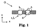
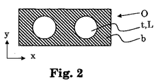
発明の詳細な説明
図1は、受動光学構成要素Oであるデバイスの断面の図式化された概略図である。図2は、図1のデバイスの上面図の図式化された概略図である。受動光学構成要素Oは、光学部材Oとも呼ぶことができ、そのように呼ぶことにする。
DETAILED DESCRIPTION OF THE INVENTION FIG. 1 is a schematic diagram of a cross section of a device that is a passive optical component O. FIG. 2 is a schematic diagram of a top view of the device of FIG. The passive optical component O can also be referred to as an optical member O and will be referred to as such.
x方向とともに垂直(z)方向が図1に示されている。図2に示される方向(x‐y平面における方向)を横方向と呼ぶ。 The vertical (z) direction as well as the x direction is shown in FIG. The direction shown in FIG. 2 (direction in the xy plane) is referred to as a horizontal direction.
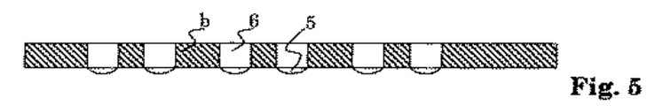
光学部材Oは、阻止部bと、2つの透明部tとを備える。実際、光学部材Oは、阻止部bと2つの透明部tとからなっている。阻止部bは、特定のスペクトル範囲(波長または波長範囲)の光に対して実質的に透過性をもたない材料、一般にポリマー材料でできているのに対して、透明部tは、少なくとも上記特定のスペクトル範囲の光に対して実質的に透過性を有する材料でできている。このように、阻止部bは、透明部tの各々のためのアパーチャとして機能し、また透明部tを固定(または保持)する。そして、後でより明らかになるように(図12参照)、阻止領域bは、上記特定のスペクトル範囲の光を実質的に減衰させるまたは阻止することによって望ましくない光から保護するためのシールドとして機能し得る。 The optical member O includes a blocking part b and two transparent parts t. Actually, the optical member O includes a blocking part b and two transparent parts t. The blocking part b is made of a material that is not substantially transparent to light in a specific spectral range (wavelength or wavelength range), generally a polymer material, whereas the transparent part t is at least the above-mentioned It is made of a material that is substantially transparent to light in a specific spectral range. In this way, the blocking part b functions as an aperture for each of the transparent parts t, and fixes (or holds) the transparent part t. And as will become more apparent later (see FIG. 12), the blocking region b functions as a shield to protect against unwanted light by substantially attenuating or blocking light in the specific spectral range. Can do.
透明部tの各々は少なくとも2つの部分を備え、図1および図2の例においては、それは、2つのレンズ素子5(またはより一般的には、光学構造5)および透明素子6の3つの部分である。これらはともにレンズ部材L(またはより一般的には、受動光学構成要素)を形成する。光学構造5は、阻止部bによって示される面から突き出ている。言い換えると、それらは、阻止部bによって示される平面を越えて垂直に延びている。光学構造5が少なくとも1つの頂点を有するレンズ素子(例えば、凹レンズ、または図1に示されるように凸レンズ)である場合、これらの頂点は光学部材Oの垂直方向断面の外側に位置する(図1)。
Each of the transparent parts t comprises at least two parts, which in the example of FIGS. 1 and 2 are the three parts of two lens elements 5 (or more generally optical structure 5) and
阻止部bは、透明素子6とともに、(完璧に近い)固体板状形状を示す。光学構造5はそこから突き出ている。透明素子6の各々は、実質的に平坦な2つの対向する側面、すなわち実質的にx‐y平面に位置する2つの面を有している。
The blocking part b has a solid plate shape (close to perfect) together with the
光学部材Oの外形は概して板状または円盤状であり、長方形の側壁を有している。
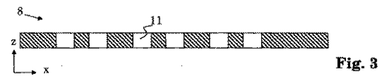
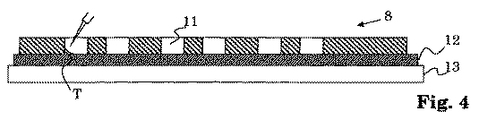
特に興味深いのは、光学部材Oおよび本発明に係る他のデバイスの製造可能性である。特に、ウェハレベルでの製造が可能である。これについては、図3〜図14を参照して説明する。
The outer shape of the optical member O is generally plate-shaped or disk-shaped, and has a rectangular side wall.
Of particular interest is the manufacturability of the optical member O and other devices according to the invention. In particular, manufacturing at the wafer level is possible. This will be described with reference to FIGS.
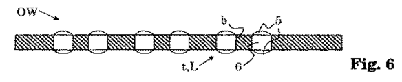
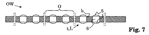
図3〜図7は、製造工程の図式化された概略断面図である。図3は、多数の孔または開口11を有する、非透明材料でできた前駆体ウェハ8を概略的に示す。一般に、これらのうちの1つ以上が長方形の格子上に配置される。製造すべき図1および図2の光学部材Oが2つの透明部tを備えるので、これら2つが長方形の格子上に配置される。
3 to 7 are schematic cross-sectional views of the manufacturing process. FIG. 3 schematically shows a
前駆体ウェハ8は、例えばエンボス加工または成形を用いて複製によって製造可能である。または、ブランクウェハは、孔あけまたはエッチングによって開口11を備えることができる。
The
なお、前駆体ウェハ8の開口11の形状は、当然のことながら、図1〜図3に示される円筒形状とは異なっていてもよい。孔11は垂直軸を有する角柱である必要はなく、横方向断面は円形である必要はない。例えば、楕円形状が可能であり、横方向断面における形状は垂直方向に沿ってさまざまであってもよく、横方向断面において孔11によって示される領域は垂直方向に沿ってさまざまであってもよい。
It should be noted that the shape of the opening 11 of the
次のステップ(図4参照)において、透明素子6は、開口11を好適な透明材料Tで充填することによって形成される。充填中、透明材料T、一般にポリマーは、液体または粘性である。スクリーン印刷から公知のものに似たスキージプロセスを用いることができ、または、例えば半導体産業から公知でありアンダーフィルのために用いられるようなディスペンサを用いることができる。ディスペンシングは1つずつ行うことができ、または、例えば透明材料Tを出力するいくつかの中空針を用いることによっていくつかの開口が同時に充填される。
In the next step (see FIG. 4), the
充填中、前駆体ウェハ8は、例えばポリジメチルシロキサンなどのシリコーンでできた支持層12上に位置する。支持層12は、機械的安定性のために剛性の支持基板13、例えばガラス板によって支持されている。
During filling, the
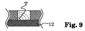
透明材料Tの充填中、材料Tに気泡または空洞が形成されないように注意しなければならない。なぜなら、透明素子6がその構成部材であるために、これによって、生成すべき受動光学構成要素Lの光学特性が劣化する可能性があるからである。例えば材料Tを出力する中空針を前駆体ウェハ8および下にある支持層12によって形成される端縁付近に好適に誘導することによって、ウェハ材料の湿潤がこのような端縁からまたはこのような端縁付近の場所で始まるように、例えばディスペンシングを行うことができる。これは図8および図9に視覚化されており、図8および図9はこの製造工程を示すための断面の図式化された概略図である。前駆体ウェハ8の材料および支持層13の材料のうち、関連する材料の特性、より特定的には透明材料Tの表面張力によって、孔11に充填されている間に材料Tによって示される形状は、さまざまであり得て、恐らくは図8および図9にそれぞれ概略的に示されているものと類似している。破線は、充填される材料Tの量の増加に伴う形状の時間的進化を示しており、図8および図9は、さまざまな湿潤角度に対するさまざまな挙動を示している。
Care must be taken that during the filling of the transparent material T no bubbles or cavities are formed in the material T. This is because, since the
充填は、十分な材料Tが充填されると中止される。次の段階に移る前に、充填された透明材料Tは、例えば熱または紫外線放射を用いて、例えばそれを硬化させることによって固められる。そのようにして得られた透明素子は、2つの(ほぼ)完璧に平面的な側面、特に(ほぼ)完璧に形成された、前駆体ウェハ8の周囲(阻止)部と共通の平面を有することができる。しかし、恐らくは、スキージを用いてもしくはディスペンシングによって達成されるかまたは異なったように達成される充填は、それほど完璧ではない可能性がある。その例が図10および図11に示されており、図10および図11は断面図の詳細の図式化された概略図である。例えば、図10に示されるように凹面が形成されてもよく、または図11に示されるように凸面が形成されてもよい。凸面の場合、次の製造工程を続ける前に研磨ステップを設けることが有利であり得る。研磨によって、突出部を少なくとも部分的に取外すことを実現することができる。また、研磨により、溢れた透明材料、すなわち充填中に所望の場所に堆積されなかった材料、例えば透明素子上に堆積されなかったが例えばわずかにそれに隣接して堆積された材料を除去することができる。
Filling is stopped when enough material T is filled. Before proceeding to the next stage, the filled transparent material T is hardened, for example by curing it, for example using heat or UV radiation. The transparent element thus obtained has two (almost) perfectly planar sides, in particular (almost) perfectly formed, and a common plane with the peripheral (blocking) part of the
代替的に、仕上げステップを伴うかまたは仕上げステップを伴わない異なる態様での透明素子6の形成を達成することもできる。支持層12によって、ウェハのその側に透明材料Tからなるいくぶん平面的な面を確保することが可能であり得るが、これを達成する他の方法も用いられてもよい。
Alternatively, the formation of the
開口11の各々が適量の固まった透明材料Tを含む場合、光学構造5はそこに設けられる(図5および図6参照)。これは、例えばWO2005/083789 A2またはUS2011/0050979 A1に記載されている当該技術分野において公知の方法において、例えば複製によって達成可能である。例えば、生成すべき光学構造5のネガを示す構造化面を有する型に好適な量の複製材料が供給され、次いで、構造化面を有する型をウェハの方に移動させ、その結果、複製材料を透明素子6と適切に接触させる。その後、例えば加熱または(紫外線などの)光による照射によって複製材料を固め、例えば硬化させ、型を除去する。(複製による、または、異なった態様での)光学構造5の形成は、一度に1つずつもしくはいくつか(しかしウェハの一方の面上の全てのうちの一部のみ)について達成されてもよく、またはウェハの一方の面上の全てについて同時に達成されてもよい。
If each of the openings 11 contains an appropriate amount of solid transparent material T, the
光学構造5は、ウェハの一方の面または両方の面に形成可能である(図5および図6参照)。光学構造5の横方向の広がりは、透明素子6の横方向の広がりよりも大きい場合もあれば小さい場合もあり、または図5および図6に示されるように実質的に同一である場合もある。光学構造5は、屈折および/または回折レンズ素子にせよプリズム素子などにせよ、事実上任意の形状のレンズ素子であり得る。多くの用途において、レンズ素子が好適な選択肢である。
The
そのようにして得られた光学ウェハOW(図6参照)は、デバイス自体であり得て、例えばさらなる製品を生成するために使用可能である。 The optical wafer OW so obtained (see FIG. 6) can be the device itself and can be used, for example, to produce further products.
例えばダイシングによって、このような光学ウェハOWを、図1および図2に示されるもののような多数の光学部材に切離すこともできる。光学ウェハOWであるデバイスの断面の図式化された概略図を示す図7において、細い破線の長方形は、切離しを行うことができる場所を示している。 Such an optical wafer OW can also be separated into a number of optical members such as those shown in FIGS. 1 and 2, for example by dicing. In FIG. 7, which shows a schematic diagram of a cross section of a device that is an optical wafer OW, a thin dashed rectangle indicates where the separation can take place.
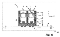
図12は、電子デバイス10であるデバイスも示す、光電子モジュール1であるデバイスの断面の図式化された概略図であり、電子デバイス10のプリント回路基板9上に実装されたこのような光電子モジュール1を備える。電子デバイス10は、例えばスマートフォンなどの手持ち式の電子通信装置、または、フォトカメラもしくはビデオカメラなどの写真装置であり得る。
FIG. 12 is a schematic diagram of a cross section of a device that is an optoelectronic module 1, also showing a device that is an
光電子モジュール1は、図1および図2に示される光学部材Oを備え、検出器D(例えばフォトダイオード)および発光体E(例えば発光ダイオード)などの少なくとも1つの能動光学構成要素も備える。能動光学構成要素D,Eは、はんだボール7を備える基板P上に実装される。とりわけ能動光学構成要素D,Eと受動光学構成要素Lとの間に好適な距離を確保するために、基板Pと光学部材Oとの間に、開口4を有する分離部材S(またはスペーサ部材S)が配置されている。その上に、バッフルとして機能する、透明領域3を有するバッフル部材Bが配置されている。
The optoelectronic module 1 comprises the optical member O shown in FIGS. 1 and 2, and also comprises at least one active optical component such as a detector D (eg a photodiode) and a light emitter E (eg a light emitting diode). Active optical components D, E are mounted on a substrate P with
上記基板P、上記光学部材O、上記バッフル部材Bおよび上記分離部材Sは、概してブロック状または板状の形状を有する(少なくとも上記分離部材Sおよび上記バッフル部材Bは、各々少なくとも1つの孔を有する)。このように、特に優れた製造可能性を実現することができる。 The substrate P, the optical member O, the baffle member B, and the separation member S generally have a block shape or a plate shape (at least the separation member S and the baffle member B each have at least one hole. ). In this way, particularly excellent manufacturability can be realized.
受動光学構成要素L、したがって透明材料Tおよび(材料Tと同一である場合もあれば、異なっている場合もある)光学構造5を構成する材料が透過性を有するが、阻止部bを構成する材料が透過性をもたない特定の波長範囲が存在する。 The passive optical component L and thus the transparent material T and the material constituting the optical structure 5 (which may be the same as or different from the material T) are transparent, but constitute the blocking part b. There are certain wavelength ranges where the material is not transparent.
例えば光電子モジュール1が近接センサである場合、発光体Eによって放出可能な光の波長範囲と光検出器Dによって検出可能な光の波長範囲との重複波長範囲が存在する。少なくともその重複波長範囲において阻止部bは透過性をもたず、少なくとも上記重複波長範囲の一部において透明部tは透過性を有する。なお、波長範囲という用語は、連続していることを暗に意味するものではない。上記重複波長範囲は、電磁スペクトルの赤外部、より具体的には近赤外部にあり得る。これは、近接センサに特に有用であり得る。 For example, when the optoelectronic module 1 is a proximity sensor, there exists an overlapping wavelength range between the wavelength range of light that can be emitted by the light emitter E and the wavelength range of light that can be detected by the photodetector D. At least in the overlapping wavelength range, the blocking part b does not have transparency, and the transparent part t has transparency in at least part of the overlapping wavelength range. The term wavelength range does not imply that it is continuous. The overlapping wavelength range may be in the infrared part of the electromagnetic spectrum, more specifically in the near infrared part. This can be particularly useful for proximity sensors.
図12に示される光電子モジュール1は、ウェハスケールで十分に製造可能である。本明細書においては、図6に示されるような光学ウェハを用いることができる。 The optoelectronic module 1 shown in FIG. 12 can be sufficiently manufactured on a wafer scale. In this specification, an optical wafer as shown in FIG. 6 can be used.
図13は、図12の多数のモジュール1を製造するためのウェハ積層体2(図14参照)を形成するためのウェハの概略断面図である。 FIG. 13 is a schematic cross-sectional view of a wafer for forming a wafer laminate 2 (see FIG. 14) for manufacturing the multiple modules 1 of FIG.
図12に示される多数のモジュール1を製造するのに、基板ウェハPW、スペーサウェハSW、(図6に示されるような)光学ウェハOWおよびバッフルウェハBWの4つのウェハで十分である。各ウェハは、対応するモジュール1(図12参照)に含まれる多数の対応する部材を備え、当該部材は、一般にウェハ切離しステップのために互いに小さな距離をあけて、通常長方形の格子上に配置されている。 Four wafers, substrate wafer PW, spacer wafer SW, optical wafer OW (as shown in FIG. 6) and baffle wafer BW, are sufficient to produce the multiple modules 1 shown in FIG. Each wafer comprises a number of corresponding members contained in a corresponding module 1 (see FIG. 12), which are generally arranged on a rectangular grid, usually at a small distance from one another for the wafer separation step. ing.
基板ウェハPWは、一方の側にはんだボール7を備え、他方の側にはんだ付けされた能動光学構成要素(EおよびD)を備える、標準的なPCB材料からなるプリント回路基板(printed circuit board:PCB)であり得る。後者は、標準的なピックアンドプレース機を用いてピックアンドプレースによって基板ウェハPW上に設置されることができる。
The substrate wafer PW comprises a printed circuit board made of standard PCB material with
光学ウェハOWを製造する方法については上で説明済みである。
望ましくない光の検出から最大限保護するために、全てのウェハPW、SW、OW、BWは、当然のことながら透明部tおよび透明領域3を除いて、検出部材Dによって検出可能な光に対して実質的に透過性をもたない材料で実質的に作られることができる。
The method for manufacturing the optical wafer OW has been described above.
In order to maximize protection from the detection of unwanted light, all wafers PW, SW, OW, BW will of course be protected against light detectable by the detection member D, with the exception of the transparent portion t and the
ウェハSWおよびBW、ならびに恐らくはウェハOWの全てまたは一部も、複製によって生成可能である。前駆体ウェハ8または透明素子6を製造するためにも用いられることができる例示的な複製プロセスにおいて、構造化面を、液体材料、粘性材料または塑性変形可能な材料にエンボス加工し、次いで例えば紫外線放射または加熱を用いた硬化によって材料を固め、次いで構造化面を除去する。このようにして、構造化面のレプリカ(この場合はネガレプリカ)が得られる。複製に適した材料は、例えば固めることが可能な(より特定的には硬化性の)ポリマー材料または他の複製材料、すなわち固めるステップ(より特定的には硬化ステップ)において液体状態、粘性状態または塑性変形可能状態から固体状態に変換可能な材料である。複製は公知の技術であり、これに関するさらなる詳細については例えばWO2005/083789 A2またはUS2011/0050979 A1を参照されたい。
Wafers SW and BW, and possibly all or part of wafer OW can also be generated by replication. In an exemplary replication process that can also be used to manufacture the
図14は、図12の多数のモジュール1を製造するためのウェハ積層体2であるデバイスの概略断面図である。 FIG. 14 is a schematic cross-sectional view of a device which is a wafer laminate 2 for manufacturing the multiple modules 1 of FIG.
ウェハ積層体2を形成するために、ウェハBW、OW、SW、PWを位置合わせし、例えば熱硬化性エポキシ樹脂を用いて貼り合わせる。位置合わせするステップは、上記検出部材Dの各々が上記透明部tのうちの少なくとも1つに対して位置合わせされるように上記基板ウェハPWおよび上記光学ウェハOWを位置合わせするステップを備え、特に上記検出部材Dの各々は、上記透明部tの各々1つに同様に位置合わせされ、同様のことが発光体Eにも当てはまる。 In order to form the wafer laminate 2, the wafers BW, OW, SW, and PW are aligned and bonded using, for example, a thermosetting epoxy resin. The step of aligning comprises the step of aligning the substrate wafer PW and the optical wafer OW such that each of the detection members D is aligned with at least one of the transparent portions t, in particular Each of the detection members D is similarly aligned with each one of the transparent portions t, and the same applies to the light emitter E.
細い破線の長方形は、例えばダイシングソーによって切離しが行われる場所を示している。 A thin dashed rectangle indicates a location where the cutting is performed by, for example, a dicing saw.
図3〜図7、図13および図14は3つのモジュール1のための構成を示しているにすぎないが、通常1つのウェハ積層体の中に、各々横方向に、少なくとも10個のモジュール、それどころか少なくとも30個のモジュール、またはさらには50個以上のモジュールのための構成がある。 3-7, 13 and 14 only show the configuration for three modules 1, but usually at least 10 modules, each laterally in one wafer stack, On the contrary, there are configurations for at least 30 modules, or even 50 or more modules.
なお、光電子モジュール1に含まれない光学部材Oを備えるデバイスについて考えることが可能である。 It is possible to consider a device including an optical member O that is not included in the optoelectronic module 1.
なお、さらに、上記の態様で得られる受動光学構成要素Lは一体型の部品ではない。それらは、そこに取付けられた少なくとも2つ、通常2つまたは3つの構成部材、すなわち透明素子6および光学構造5を備える。しかし、透明素子6は通常は一体型の部品である。
Furthermore, the passive optical component L obtained in the above aspect is not an integral part. They comprise at least two, usually two or three components attached thereto, namely a
前駆体ウェハ8に透明素子6を設けることによって得られる半完成品(特定の見方では、本発明に係るデバイスでもあり得る)は、通常、ウェハを貫通する孔をもたない(または、少なくとも透明部tがある領域においてウェハを貫通する孔をもたない)平坦な円盤状ウェハである。
The semi-finished product obtained by providing the
半完成品は、それらの領域に浅い表面波形を事実上もたない場合もあれば、浅い表面波形のみを有する場合もあり、このような表面波形は、存在する場合には、通常凹状である(図10参照)。すなわち、このような表面波形は、少なくとも1つの阻止部bによって示されるウェハ面を越えて延びていない。恐らく形成される凸状メニスカスは、研磨によって例えば上記のように平坦化可能であり、その結果、ウェハ厚みに調整された平行な面を有する透明素子6が得られ、恐らくはウェハ厚みも調整(低減)することができる。
Semi-finished products may have virtually no shallow surface corrugations in their area, or only have shallow surface corrugations, such surface corrugations are usually concave when present. (See FIG. 10). That is, such a surface waveform does not extend beyond the wafer surface indicated by the at least one blocking portion b. The formed convex meniscus can be planarized by polishing, for example, as described above, resulting in a
しかし、代替的に、半完成品は、一方の面または両方の面に、特に透明部tがあるそれらの領域に、構造化面を有していてもよい。阻止部bには望ましい波形が存在し得る。特に、(記載した光学ウェハOWなどの)光学ウェハと(記載したスペーサウェハSWなどの)スペーサウェハとの組合せであるウェハ、すなわち「結合光学ウェハ」を設けることができる。したがって、その場合、スペーサウェハは任意であり、その特性および機能は、それに応じて構造化され構成される光学ウェハ(「結合光学ウェハ」)によって実現される。これは、例えばスペーサウェハSWとして上記したものと少なくとも1つの阻止部bとして上記したものとを一体型の部品として製造することによって達成可能である。対応する光学ウェハ(「結合光学ウェハ」)は、図14におけるウェハOWおよびSWを1つの単一の部品として見ると容易に視覚化可能である。好適な半完成品、すなわち「結合半完成品」から出発して、「結合光学ウェハ」は、例えばディスペンシングによって、例えば上記のように光学構造をその上に(「結合半完成品」の透明部上に)生成することによって得ることができる。 Alternatively, however, the semi-finished product may have a structured surface on one or both surfaces, in particular in those areas where there is a transparent part t. There may be a desired waveform in the blocking part b. In particular, a wafer that is a combination of an optical wafer (such as the described optical wafer OW) and a spacer wafer (such as the described spacer wafer SW), ie a “coupled optical wafer” can be provided. Thus, in that case, the spacer wafer is optional, and its properties and functions are realized by an optical wafer (“coupled optical wafer”) structured and configured accordingly. This can be achieved, for example, by manufacturing the spacer wafer SW as described above and the at least one blocking portion b as an integral part. Corresponding optical wafers (“coupled optical wafers”) can be easily visualized when viewing wafers OW and SW in FIG. 14 as one single piece. Starting from a suitable semi-finished product, i.e. "bonded semi-finished product", a "bonded optical wafer" is produced by placing an optical structure thereon (e.g. transparent of "bonded semi-finished product"), for example by dispensing. On the part).
「結合半完成品」の別の例(ow’として参照される)が図16に示されているのに対して、図3〜図7および図12〜図14に関連して説明したものにより密接に対応する半完成品owが図15に示されている。 Another example of a “combined semi-finished product” (referred to as ow ′) is shown in FIG. 16, whereas that described in connection with FIGS. 3-7 and 12-14. A semi-finished product ow that closely corresponds is shown in FIG.
さらに、(記載した光学ウェハOWなどの)光学ウェハと(記載したバッフルウェハBWなどの)バッフルウェハとの組合せである光学ウェハ(「結合光学ウェハ」)を設けることができる。したがって、その場合、バッフルウェハは任意であり、その特性および機能は、それに応じて構造化され構成される光学ウェハ(「結合光学ウェハ」)によって実現される。これは、例えばバッフルウェハBWとして上記したものと少なくとも1つの阻止部bとして上記したものとを一体型の部品として製造することによって達成可能である。対応する光学ウェハは、図14におけるウェハOWおよびBWを1つの単一の部品として見ると容易に視覚化可能である。好適な「結合半完成品」は、図16に示されるものと類似していてもよい。 Furthermore, an optical wafer ("coupled optical wafer") that is a combination of an optical wafer (such as the described optical wafer OW) and a baffle wafer (such as the described baffle wafer BW) can be provided. Thus, in that case, the baffle wafer is optional, and its properties and functions are realized by an optical wafer (“coupled optical wafer”) structured and constructed accordingly. This can be achieved, for example, by manufacturing the baffle wafer BW described above and the at least one blocking portion b described above as an integral part. Corresponding optical wafers can be easily visualized when viewing wafers OW and BW in FIG. 14 as one single piece. A suitable “joint semi-finished product” may be similar to that shown in FIG.
当然のことながら、例えば図14の実施例においてバッフルウェハBWおよびスペーサウェハSWを旧式化するように、光学ウェハ(「結合光学ウェハ」)の両面を構造化することもできる。 Of course, both sides of the optical wafer ("coupled optical wafer") can be structured, for example, to make the baffle wafer BW and spacer wafer SW obsolete in the embodiment of FIG.
(半完成品を得るために)透明素子6を形成するために片面または両面が構造化された前駆体ウェハに透明材料Tを充填することは、図4に示されるもの(および図16において支持層12によって示唆されるもの)と同様に達成可能であり、図16においては、「結合半完成品」ow’の構造化されていない側が支持層12に対向している。代替的に、充填された材料が前駆体ウェハの開口を(過剰に激しく)流れることを回避するために、透明素子6を形成している間、構造化された支持層12を用いることができる。後者の処理は、両面に構造化面を有する前駆体ウェハが透明素子6を備えている場合に特に有用であり得る。
Filling a transparent wafer T with a precursor wafer structured on one or both sides to form a transparent element 6 (to obtain a semi-finished product) is shown in FIG. 4 (and supported in FIG. 16). In FIG. 16, the unstructured side of the “bonded semi-finished product” ow ′ faces the
ウェハについて今しがた行った説明に対応して、「結合光学部材」も設けることができる。光学部材の阻止部は、構造化面、特に「結合光学部材」の透明素子の面を越えて垂直に突き出る突出部を有する面を有し得る。上記の光学部材と上記の分離部材との組合せ(または記載した光学部材と記載したバッフル部材との組合せ、または3つ全ての組合せ)である部材(「結合光学部材」)を設けることができる。したがって、その場合、分離部材(および/またはバッフル部材)は任意であり、その特性および機能は、それに応じて構造化され構成される光学部材によって実現される。これは、例えば分離部材Sとして上記したもの(および/またはバッフル部材Bとして上記したもの)と少なくとも1つの阻止部bとして上記したものとを一体型の部品として製造することによって達成可能である。 Corresponding to the explanation just given for the wafer, a “coupled optical member” can also be provided. The blocking part of the optical member may have a structured surface, in particular a surface with protrusions that protrude perpendicularly beyond the surface of the transparent element of the “coupled optical member”. A member (“coupled optical member”) that is a combination of the optical member and the separating member (or a combination of the described optical member and a baffle member or a combination of all three) may be provided. Thus, in that case, the separating member (and / or baffle member) is optional and its properties and functions are realized by the optical member structured and configured accordingly. This can be achieved, for example, by manufacturing the separation member S described above (and / or the baffle member B described above) and the at least one blocking portion b described above as an integral part.
このような「結合光学部材」または「結合光学ウェハ」を設けることの通常の結果は、(モジュール1などの構造化すべき要素の)部品の数および組立工程の数が低減されて、通常は位置合わせ誤差がそれほど起こらなくなることである。 The usual result of providing such a “coupled optical member” or “coupled optical wafer” is that the number of parts (of the element to be structured such as module 1) and the number of assembly steps are reduced, usually in position. The alignment error is less likely to occur.
図15に戻って、そこに示される半完成品owは、一方の面または両方の面に研磨ステップが施されることができる。研磨ステップは、例えばウェハowを薄くして(厳密に)所望の厚みにするように、および/または、(少なくとも透明素子6の)光学特性を向上させるように達成可能である。当然のことながら、片面が構造化された半完成品も、少なくともその平坦な(構造化されていない)側を研磨することができる。 Returning to FIG. 15, the semi-finished product ow shown therein may be subjected to a polishing step on one or both sides. The polishing step can be achieved, for example, to make the wafer ow thinner (strictly) to the desired thickness and / or to improve the optical properties (at least of the transparent element 6). Of course, a semi-finished product with one side structured can also be polished at least on its flat (unstructured) side.
なお、さらに、前駆体ウェハは、一方の面または両方の面において、少なくとも少なくとも一方の平坦な側を研磨することができる。そのようにすることは、前駆体ウェハのより平坦なおよび/またはより平らな面に貢献する可能性があるだけでなく、前駆体ウェハの厚みを所望の厚みに減少させることを可能にし得て、これは見込まれるその後の製造工程で役立ち得る。 Further, at least one flat side of the precursor wafer can be polished on one side or both sides. Doing so may not only contribute to a flatter and / or flatter surface of the precursor wafer, but may allow the thickness of the precursor wafer to be reduced to a desired thickness. This can be useful in the subsequent manufacturing process that is expected.
(「結合半完成品」であろうと、そうでなかろうと)半完成品自体がデバイスであり、透明素子6上に光学構造を生成することなく用いられる場合、光学グレード面(optical grade surface)を実現するように一方の面または両方の面を研磨することが有用であり得て、特に面は、特に平面であり、特に小さな表面粗さを有する。
If the semi-finished product itself is a device (whether or not “bonded semi-finished product”) and is used without creating an optical structure on the
光学ウェハを得るために、透明材料Tからなる凹状メニスカスが存在する光学構造5が(例えば複製によって)半完成品に設けられる場合、複製はこれらのメニスカス上で行われることができ、適用される複製材料の量はそれに応じて調整されなければならないかもしれない。対応する半完成品が研磨されれば、明確に規定された平坦な面を得ることができ、その後の複製ステップにおいてそれほどばらつきがみられなくなる。したがって、複製がより容易に行われるものと考えられ、および/または、より安定した(および再現可能な)プロセスをもたらし、恐らくはより優れた精度をもたらし得る。
In order to obtain optical wafers, if
上記のどこかに記載した製造プロセス中に固められる、特に硬化する材料は、一般に、エポキシ樹脂などのポリマーベースの材料である。 Particularly hardened materials that are hardened during the manufacturing process described anywhere above are generally polymer-based materials such as epoxy resins.
ウェハレベルでの製造のために、大半の位置合わせステップはウェハレベルで行われ、これにより、かなり簡単かつ非常に速い態様で(特に受動光学構成要素Lに対する部材DおよびEの)非常に優れた位置合わせを実現することが可能になる。製造プロセス全体は、非常に速く正確である。ウェハスケールでの製造のために、多数のモジュール1および/または多数の光学部材Oを製造するのに非常に少ない数の生成工程しか必要とされない。 For wafer level manufacturing, most of the alignment steps are performed at the wafer level, which results in a very simple and very fast manner (especially for members D and E for passive optical components L). It becomes possible to realize alignment. The entire manufacturing process is very fast and accurate. Due to the production on the wafer scale, a very small number of production steps are required to produce a large number of modules 1 and / or a large number of optical elements O.
光学部材O(および同様に上記の他のデバイス)は多くの用途、特にアパーチャが適用される用途および/または光からの保護が求められる用途および/または大量生産が必要な用途および/または特に小さな光学部材(または受動光学構成要素)が必要とされる用途において有用であり得る。 The optical member O (and also the other devices mentioned above) can be used in many applications, particularly in applications where apertures are applied and / or applications where protection from light is required and / or where mass production is required and / or particularly small. It may be useful in applications where an optical member (or passive optical component) is required.
1 デバイス,光電子モジュール、2 デバイス,ウェハ積層体、3 透明領域、4 開口、5 光学構造,レンズ素子、6 透明素子、7 はんだボール、8 前駆体ウェハ、9 プリント回路基板、10 デバイス,電子デバイス,スマートフォン、11 孔,開口、12 支持層、13 支持基板、b 阻止部,非透明部、B バッフル部材、BW バッフルウェハ、D 検出器,光検出器,フォトダイオード、E 発光体,発光ダイオード、L 受動光学構成要素,レンズ部材、O デバイス,光学部材、ow デバイス,半完成品、ow’ デバイス,半完成品,「結合半完成品」、OW デバイス,光学ウェハ、P 基板、PW 基板ウェハ、S 分離部材、SW スペーサウェハ、t 透明部、T 透明材料。 1 device, optoelectronic module, 2 device, wafer laminate, 3 transparent region, 4 aperture, 5 optical structure, lens element, 6 transparent element, 7 solder ball, 8 precursor wafer, 9 printed circuit board, 10 device, electronic device , Smartphone, 11 hole, opening, 12 support layer, 13 support substrate, b blocking part, non-transparent part, B baffle member, BW baffle wafer, D detector, photodetector, photodiode, E emitter, light emitting diode, L Passive optical component, lens member, O device, optical member, ow device, semi-finished product, ow 'device, semi-finished product, “joint semi-finished product”, OW device, optical wafer, P substrate, PW substrate wafer, S separation member, SW spacer wafer, t transparent part, T transparent material.
Claims (25)
a)少なくとも1つの阻止部と多数の透明素子とを備えるウェハを設けるステップを備え、
前記多数の透明素子の各々は、透明材料と呼ばれる、少なくとも特定のスペクトル範囲の光に対して実質的に透過性を有する1つ以上の材料でできており、前記少なくとも1つの阻止部は、非透明材料と呼ばれる、前記特定のスペクトル範囲の光に対して実質的に透過性をもたない1つ以上の材料でできている、方法。 A method of manufacturing a device comprising at least one passive optical component, the method comprising:
a) providing a wafer comprising at least one blocking part and a number of transparent elements;
Each of the multiple transparent elements is made of one or more materials, called transparent materials, that are substantially transparent to light in at least a specific spectral range, and the at least one blocking portion is non- A method made of one or more materials, referred to as transparent materials, that are not substantially transparent to light in the specific spectral range.
ステップd)は、
d1)前記透明素子が位置することになる場所に開口を有する、実質的に前記非透明材料でできた前駆体ウェハを設けるステップと、
d2)前記開口を前記透明材料のうちの少なくとも1つで少なくとも部分的に充填するステップとを備える、請求項1または2に記載の方法。 d) comprising the step of manufacturing the wafer;
Step d)
d1) providing a precursor wafer substantially made of the non-transparent material having an opening where the transparent element will be located;
d2) at least partially filling the opening with at least one of the transparent materials.
ステップc)は、
c1)前記多数の透明素子の各々の上に少なくとも1つの光学構造を生成することによって前記多数の受動光学構成要素を生成するステップを備える、請求項1から5のいずれか1項に記載の方法。 c) manufacturing a wafer called an optical wafer comprising a number of passive optical components comprising said at least one passive optical component;
Step c)
6. The method of any one of claims 1-5, comprising c1) generating the multiple passive optical components by generating at least one optical structure on each of the multiple transparent elements. .
f)前記ウェハ積層体を切離すことによって、各々が前記多数の受動光学構成要素のうちの少なくとも1つを備える多数の別々のモジュールを得るステップとを備える、請求項6から8のいずれか1項に記載の方法。 e) providing a wafer stack comprising the optical wafer and at least one further wafer;
f) obtaining a number of separate modules each comprising at least one of the number of passive optical components by separating the wafer stack. The method according to item.
Applications Claiming Priority (3)
| Application Number | Priority Date | Filing Date | Title |
|---|---|---|---|
| US201161509357P | 2011-07-19 | 2011-07-19 | |
| US61/509,357 | 2011-07-19 | ||
| PCT/CH2012/000160 WO2013010285A1 (en) | 2011-07-19 | 2012-07-10 | Method for manufacturing passive optical components, and devices comprising the same |
Related Child Applications (1)
| Application Number | Title | Priority Date | Filing Date |
|---|---|---|---|
| JP2017042941A Division JP6763807B2 (en) | 2011-07-19 | 2017-03-07 | Manufacturing methods for passive optics and devices with passive optics |
Publications (2)
| Publication Number | Publication Date |
|---|---|
| JP2014521992A true JP2014521992A (en) | 2014-08-28 |
| JP2014521992A5 JP2014521992A5 (en) | 2015-08-13 |
Family
ID=46639253
Family Applications (2)
| Application Number | Title | Priority Date | Filing Date |
|---|---|---|---|
| JP2014520486A Pending JP2014521992A (en) | 2011-07-19 | 2012-07-10 | Method for manufacturing passive optical component and device comprising passive optical component |
| JP2017042941A Active JP6763807B2 (en) | 2011-07-19 | 2017-03-07 | Manufacturing methods for passive optics and devices with passive optics |
Family Applications After (1)
| Application Number | Title | Priority Date | Filing Date |
|---|---|---|---|
| JP2017042941A Active JP6763807B2 (en) | 2011-07-19 | 2017-03-07 | Manufacturing methods for passive optics and devices with passive optics |
Country Status (8)
| Country | Link |
|---|---|
| US (4) | US8767303B2 (en) |
| EP (1) | EP2735029B1 (en) |
| JP (2) | JP2014521992A (en) |
| KR (1) | KR101966478B1 (en) |
| CN (1) | CN103975436B (en) |
| SG (1) | SG10201605834YA (en) |
| TW (3) | TWI647825B (en) |
| WO (1) | WO2013010285A1 (en) |
Cited By (3)
| Publication number | Priority date | Publication date | Assignee | Title |
|---|---|---|---|---|
| JP2014521226A (en) * | 2011-07-19 | 2014-08-25 | ヘプタゴン・マイクロ・オプティクス・プライベート・リミテッド | Optoelectronic module, optoelectronic module manufacturing method, and apparatus and device including the optoelectronic module |
| JP2017022200A (en) * | 2015-07-08 | 2017-01-26 | ソニーセミコンダクタソリューションズ株式会社 | Image sensor, and electronic apparatus |
| JP2017143211A (en) * | 2016-02-12 | 2017-08-17 | 凸版印刷株式会社 | Solid-state image pickup element and method of manufacturing the same |
Families Citing this family (14)
| Publication number | Priority date | Publication date | Assignee | Title |
|---|---|---|---|---|
| CN103858230B (en) * | 2011-08-10 | 2018-03-27 | 新加坡恒立私人有限公司 | Optoelectronic module and the method for manufacturing the optoelectronic module |
| US9634050B2 (en) | 2012-08-20 | 2017-04-25 | Heptagon Micro Optics Pte. Ltd. | Fabrication of optics wafer |
| EP2827368B1 (en) * | 2013-07-19 | 2019-06-05 | ams AG | Package for an optical sensor, optical sensor arrangement and method of producing a package for an optical sensor |
| US11036309B2 (en) | 2013-07-31 | 2021-06-15 | Ams Sensors Singapore Pte. Ltd. | Micro-optical orientation sensor and related methods |
| NL2011843C2 (en) | 2013-11-26 | 2015-05-27 | Anteryon Wafer Optics B V | A method for manufacturing an optical assembly. |
| US9711552B2 (en) * | 2014-08-19 | 2017-07-18 | Heptagon Micro Optics Pte. Ltd. | Optoelectronic modules having a silicon substrate, and fabrication methods for such modules |
| US9829614B2 (en) | 2015-02-02 | 2017-11-28 | Synaptics Incorporated | Optical sensor using collimator |
| US20160307881A1 (en) * | 2015-04-20 | 2016-10-20 | Advanced Semiconductor Engineering, Inc. | Optical sensor module and method for manufacturing the same |
| JPWO2016208403A1 (en) * | 2015-06-23 | 2018-04-12 | ソニー株式会社 | Image sensor and electronic device |
| JP2018537845A (en) * | 2015-10-07 | 2018-12-20 | シナプティクス インコーポレイテッド | Image sensor structure for fingerprint detection |
| KR101738883B1 (en) * | 2016-01-06 | 2017-05-23 | 한국과학기술원 | Ultrathin digital camera and manufacturing method of the same |
| WO2017155460A1 (en) * | 2016-03-08 | 2017-09-14 | Tnc Optics & Technologies Pte. Ltd. | A fabrication method of optical sensor cover having a lens |
| CN113474154A (en) * | 2019-02-25 | 2021-10-01 | ams传感器新加坡私人有限公司 | Production of an optical diffuser element and optical diffuser element |
| US10734184B1 (en) | 2019-06-21 | 2020-08-04 | Elbit Systems Of America, Llc | Wafer scale image intensifier |
Citations (10)
| Publication number | Priority date | Publication date | Assignee | Title |
|---|---|---|---|---|
| JPS5590909A (en) * | 1978-12-28 | 1980-07-10 | Canon Inc | Production of compound eye lens device |
| JPH02137802A (en) * | 1988-10-14 | 1990-05-28 | Corning Inc | Integrated optical element and manufacture thereof |
| JP2003004909A (en) * | 2001-04-20 | 2003-01-08 | Matsushita Electric Ind Co Ltd | Microlens array and method for manufacturing it |
| JP2005072662A (en) * | 2003-08-25 | 2005-03-17 | Sharp Corp | Light transmitting plate and manufacturing method thereof, image input apparatus using light transmitting plate |
| US20080290435A1 (en) * | 2007-05-21 | 2008-11-27 | Micron Technology, Inc. | Wafer level lens arrays for image sensor packages and the like, image sensor packages, and related methods |
| US20090219632A1 (en) * | 2008-02-28 | 2009-09-03 | Kang Wei-Hung | Lens module and a method for fabricating the same |
| JP2010204635A (en) * | 2009-02-06 | 2010-09-16 | Fujifilm Corp | Lens array |
| WO2010139342A1 (en) * | 2009-06-02 | 2010-12-09 | Fraunhofer-Gesellschaft zur Förderung der angewandten Forschung e. V. | Lens and method for manufacturing same |
| JP2011508253A (en) * | 2007-12-19 | 2011-03-10 | ヘプタゴン・オサケ・ユキチュア | Optical element manufacturing |
| US7974023B1 (en) * | 2010-03-11 | 2011-07-05 | Himax Semiconductor, Inc. | Wafer level optical lens substrate, wafer level optical lens module and fabrication method thereof |
Family Cites Families (27)
| Publication number | Priority date | Publication date | Assignee | Title |
|---|---|---|---|---|
| US3532038A (en) * | 1967-06-05 | 1970-10-06 | Ibm | Multi-lens devices for the fabrication of semiconductor devices |
| BR9510290A (en) * | 1994-12-23 | 1997-11-11 | Digirad | Semiconductor gamma ray camera and medical imaging system |
| DE60200225T2 (en) * | 2001-04-20 | 2004-07-15 | Matsushita Electric Industrial Co., Ltd., Kadoma | Microlens array and method for its manufacture |
| TW200506418A (en) * | 2003-07-01 | 2005-02-16 | Nippon Sheet Glass Co Ltd | Lens plate, its manufacturing method, and image transmitting apparatus |
| EP1569276A1 (en) | 2004-02-27 | 2005-08-31 | Heptagon OY | Micro-optics on optoelectronics |
| US7399421B2 (en) * | 2005-08-02 | 2008-07-15 | International Business Machines Corporation | Injection molded microoptics |
| JP2007148297A (en) * | 2005-11-30 | 2007-06-14 | Hitachi Maxell Ltd | Optical sheet for backlight, backlight and display device |
| KR100802199B1 (en) * | 2006-05-25 | 2008-03-17 | 정경희 | Optical module and fabrication method of the same |
| EP1870936A1 (en) * | 2006-06-19 | 2007-12-26 | STMicroelectronics (Rousset) SAS | Method to produce lenses, particularly for integrated imager |
| US8013289B2 (en) * | 2006-11-15 | 2011-09-06 | Ether Precision, Inc. | Lens array block for image capturing unit and methods of fabrication |
| US20110031510A1 (en) * | 2007-11-27 | 2011-02-10 | Heptagon Oy | Encapsulated lens stack |
| TWI505703B (en) * | 2007-12-19 | 2015-10-21 | Heptagon Micro Optics Pte Ltd | Optical module, wafer scale package, and method for manufacturing those |
| JP5030828B2 (en) * | 2008-03-18 | 2012-09-19 | 株式会社沖データ | Lens array and LED head, exposure apparatus, image forming apparatus and reading apparatus having the same |
| WO2009133756A1 (en) * | 2008-04-28 | 2009-11-05 | コニカミノルタオプト株式会社 | Method for producing wafer lens assembly and method for producing wafer lens |
| JP4906798B2 (en) * | 2008-07-01 | 2012-03-28 | 株式会社沖データ | Lens array, LED head, exposure apparatus, image forming apparatus, and reading apparatus |
| JP4966931B2 (en) * | 2008-08-26 | 2012-07-04 | シャープ株式会社 | Electronic element wafer module and manufacturing method thereof, electronic element module and manufacturing method thereof, electronic information device |
| WO2010055801A1 (en) | 2008-11-17 | 2010-05-20 | コニカミノルタオプト株式会社 | Optical element manufacturing method and optical element |
| JP2010204632A (en) | 2009-02-06 | 2010-09-16 | Fujifilm Corp | Method of manufacturing wafer level lens array, wafer lens array, lens module and imaging unit |
| CN102023330A (en) * | 2009-09-15 | 2011-04-20 | 鸿富锦精密工业(深圳)有限公司 | Shading element array, method for manufacturing shading element array and lens module array |
| JP2011097294A (en) | 2009-10-28 | 2011-05-12 | Olympus Corp | Imaging apparatus and method for manufacturing the same |
| CN102667568A (en) | 2009-11-05 | 2012-09-12 | 柯尼卡美能达先进多层薄膜株式会社 | Image pickup device and method for manufacturing the image pickup device |
| JP2011104811A (en) | 2009-11-13 | 2011-06-02 | Fujifilm Corp | Master die, method of preparing master and the master |
| CN104317164B (en) * | 2009-12-11 | 2018-03-30 | 富士胶片株式会社 | Black curable composition |
| CN102130138B (en) * | 2010-01-12 | 2013-01-02 | 中芯国际集成电路制造(上海)有限公司 | Image sensor and forming method thereof |
| TWM399313U (en) * | 2010-07-30 | 2011-03-01 | Sigurd Microelectronics Corp | Proximity sensor package structure |
| WO2013049948A1 (en) * | 2011-10-06 | 2013-04-11 | Heptagon Micro Optics Pte. Ltd. | Method for wafer-level manufacturing of objects and corresponding semi-finished products |
| JP2014190988A (en) * | 2013-03-26 | 2014-10-06 | Fuji Xerox Co Ltd | Lens array and lens array manufacturing method |
-
2012
- 2012-07-10 JP JP2014520486A patent/JP2014521992A/en active Pending
- 2012-07-10 WO PCT/CH2012/000160 patent/WO2013010285A1/en active Application Filing
- 2012-07-10 CN CN201280045590.9A patent/CN103975436B/en active Active
- 2012-07-10 EP EP12743875.2A patent/EP2735029B1/en active Active
- 2012-07-10 KR KR1020147004151A patent/KR101966478B1/en active IP Right Grant
- 2012-07-10 SG SG10201605834YA patent/SG10201605834YA/en unknown
- 2012-07-17 TW TW106126425A patent/TWI647825B/en active
- 2012-07-17 TW TW101125645A patent/TWI635601B/en active
- 2012-07-17 TW TW106113502A patent/TWI647824B/en active
- 2012-07-19 US US13/553,385 patent/US8767303B2/en active Active
-
2014
- 2014-05-28 US US14/288,755 patent/US9193120B2/en active Active
-
2015
- 2015-10-14 US US14/882,905 patent/US9610743B2/en active Active
-
2017
- 2017-02-24 US US15/441,515 patent/US10527762B2/en active Active
- 2017-03-07 JP JP2017042941A patent/JP6763807B2/en active Active
Patent Citations (11)
| Publication number | Priority date | Publication date | Assignee | Title |
|---|---|---|---|---|
| JPS5590909A (en) * | 1978-12-28 | 1980-07-10 | Canon Inc | Production of compound eye lens device |
| JPH02137802A (en) * | 1988-10-14 | 1990-05-28 | Corning Inc | Integrated optical element and manufacture thereof |
| JP2003004909A (en) * | 2001-04-20 | 2003-01-08 | Matsushita Electric Ind Co Ltd | Microlens array and method for manufacturing it |
| JP2005072662A (en) * | 2003-08-25 | 2005-03-17 | Sharp Corp | Light transmitting plate and manufacturing method thereof, image input apparatus using light transmitting plate |
| US20080290435A1 (en) * | 2007-05-21 | 2008-11-27 | Micron Technology, Inc. | Wafer level lens arrays for image sensor packages and the like, image sensor packages, and related methods |
| JP2011508253A (en) * | 2007-12-19 | 2011-03-10 | ヘプタゴン・オサケ・ユキチュア | Optical element manufacturing |
| US20090219632A1 (en) * | 2008-02-28 | 2009-09-03 | Kang Wei-Hung | Lens module and a method for fabricating the same |
| JP2010204635A (en) * | 2009-02-06 | 2010-09-16 | Fujifilm Corp | Lens array |
| WO2010139342A1 (en) * | 2009-06-02 | 2010-12-09 | Fraunhofer-Gesellschaft zur Förderung der angewandten Forschung e. V. | Lens and method for manufacturing same |
| JP2012529069A (en) * | 2009-06-02 | 2012-11-15 | フラウンホーファー−ゲゼルシャフト・ツール・フェルデルング・デル・アンゲヴァンテン・フォルシュング・アインゲトラーゲネル・フェライン | Lens and manufacturing method thereof |
| US7974023B1 (en) * | 2010-03-11 | 2011-07-05 | Himax Semiconductor, Inc. | Wafer level optical lens substrate, wafer level optical lens module and fabrication method thereof |
Cited By (4)
| Publication number | Priority date | Publication date | Assignee | Title |
|---|---|---|---|---|
| JP2014521226A (en) * | 2011-07-19 | 2014-08-25 | ヘプタゴン・マイクロ・オプティクス・プライベート・リミテッド | Optoelectronic module, optoelectronic module manufacturing method, and apparatus and device including the optoelectronic module |
| JP2017022200A (en) * | 2015-07-08 | 2017-01-26 | ソニーセミコンダクタソリューションズ株式会社 | Image sensor, and electronic apparatus |
| US11262485B2 (en) | 2015-07-08 | 2022-03-01 | Sony Semiconductor Solutions Corporation | Image sensor and electronic apparatus |
| JP2017143211A (en) * | 2016-02-12 | 2017-08-17 | 凸版印刷株式会社 | Solid-state image pickup element and method of manufacturing the same |
Also Published As
| Publication number | Publication date |
|---|---|
| TW201820597A (en) | 2018-06-01 |
| TW201742238A (en) | 2017-12-01 |
| EP2735029B1 (en) | 2022-12-21 |
| US20130033767A1 (en) | 2013-02-07 |
| TWI635601B (en) | 2018-09-11 |
| US9193120B2 (en) | 2015-11-24 |
| US20160031169A1 (en) | 2016-02-04 |
| US8767303B2 (en) | 2014-07-01 |
| EP2735029A1 (en) | 2014-05-28 |
| US20170235026A1 (en) | 2017-08-17 |
| WO2013010285A1 (en) | 2013-01-24 |
| KR101966478B1 (en) | 2019-04-05 |
| US10527762B2 (en) | 2020-01-07 |
| JP6763807B2 (en) | 2020-09-30 |
| SG10201605834YA (en) | 2016-09-29 |
| US20140347747A1 (en) | 2014-11-27 |
| CN103975436A (en) | 2014-08-06 |
| KR20140054081A (en) | 2014-05-08 |
| JP2017167533A (en) | 2017-09-21 |
| TW201310626A (en) | 2013-03-01 |
| TWI647824B (en) | 2019-01-11 |
| US9610743B2 (en) | 2017-04-04 |
| TWI647825B (en) | 2019-01-11 |
| CN103975436B (en) | 2019-05-10 |
Similar Documents
| Publication | Publication Date | Title |
|---|---|---|
| JP6763807B2 (en) | Manufacturing methods for passive optics and devices with passive optics | |
| US11005001B2 (en) | Opto-electronic modules and methods of manufacturing the same and appliances and devices comprising the same | |
| JP6247633B2 (en) | Optoelectronic module and manufacturing method thereof | |
| KR102125532B1 (en) | Reflowable opto-electronic module | |
| JP4903685B2 (en) | Method for manufacturing an integrated optical system | |
| US10180235B2 (en) | Optical module, in particular opto-electronic module, and method of manufacturing the same | |
| TWI624040B (en) | Fabrication of optics wafer |
Legal Events
| Date | Code | Title | Description |
|---|---|---|---|
| A521 | Request for written amendment filed |
Free format text: JAPANESE INTERMEDIATE CODE: A523 Effective date: 20150624 |
|
| A621 | Written request for application examination |
Free format text: JAPANESE INTERMEDIATE CODE: A621 Effective date: 20150624 |
|
| A977 | Report on retrieval |
Free format text: JAPANESE INTERMEDIATE CODE: A971007 Effective date: 20160315 |
|
| A131 | Notification of reasons for refusal |
Free format text: JAPANESE INTERMEDIATE CODE: A131 Effective date: 20160405 |
|
| A521 | Request for written amendment filed |
Free format text: JAPANESE INTERMEDIATE CODE: A523 Effective date: 20160624 |
|
| A02 | Decision of refusal |
Free format text: JAPANESE INTERMEDIATE CODE: A02 Effective date: 20161108 |