JP2005294444A - Semiconductor device and manufacturing method thereof, pseudo wafer and manufacturing method thereof, and mounting structure of semiconductor device and mounting method thereof - Google Patents
Semiconductor device and manufacturing method thereof, pseudo wafer and manufacturing method thereof, and mounting structure of semiconductor device and mounting method thereof Download PDFInfo
- Publication number
- JP2005294444A JP2005294444A JP2004105835A JP2004105835A JP2005294444A JP 2005294444 A JP2005294444 A JP 2005294444A JP 2004105835 A JP2004105835 A JP 2004105835A JP 2004105835 A JP2004105835 A JP 2004105835A JP 2005294444 A JP2005294444 A JP 2005294444A
- Authority
- JP
- Japan
- Prior art keywords
- semiconductor device
- chip component
- support
- manufacturing
- chip
- Prior art date
- Legal status (The legal status is an assumption and is not a legal conclusion. Google has not performed a legal analysis and makes no representation as to the accuracy of the status listed.)
- Pending
Links
Images
Classifications
-
- H—ELECTRICITY
- H10—SEMICONDUCTOR DEVICES; ELECTRIC SOLID-STATE DEVICES NOT OTHERWISE PROVIDED FOR
- H10W—GENERIC PACKAGES, INTERCONNECTIONS, CONNECTORS OR OTHER CONSTRUCTIONAL DETAILS OF DEVICES COVERED BY CLASS H10
- H10W72/00—Interconnections or connectors in packages
- H10W72/01—Manufacture or treatment
- H10W72/0198—Manufacture or treatment batch processes
-
- H—ELECTRICITY
- H10—SEMICONDUCTOR DEVICES; ELECTRIC SOLID-STATE DEVICES NOT OTHERWISE PROVIDED FOR
- H10W—GENERIC PACKAGES, INTERCONNECTIONS, CONNECTORS OR OTHER CONSTRUCTIONAL DETAILS OF DEVICES COVERED BY CLASS H10
- H10W46/00—Marks applied to devices, e.g. for alignment or identification
- H10W46/301—Marks applied to devices, e.g. for alignment or identification for alignment
-
- H—ELECTRICITY
- H10—SEMICONDUCTOR DEVICES; ELECTRIC SOLID-STATE DEVICES NOT OTHERWISE PROVIDED FOR
- H10W—GENERIC PACKAGES, INTERCONNECTIONS, CONNECTORS OR OTHER CONSTRUCTIONAL DETAILS OF DEVICES COVERED BY CLASS H10
- H10W70/00—Package substrates; Interposers; Redistribution layers [RDL]
- H10W70/01—Manufacture or treatment
- H10W70/05—Manufacture or treatment of insulating or insulated package substrates, or of interposers, or of redistribution layers
- H10W70/08—Manufacture or treatment of insulating or insulated package substrates, or of interposers, or of redistribution layers by depositing layers on the chip or wafer, e.g. "chip-first" RDLs
- H10W70/09—Manufacture or treatment of insulating or insulated package substrates, or of interposers, or of redistribution layers by depositing layers on the chip or wafer, e.g. "chip-first" RDLs extending onto an encapsulation that laterally surrounds the chip or wafer, e.g. fan-out wafer level package [FOWLP] RDLs
-
- H—ELECTRICITY
- H10—SEMICONDUCTOR DEVICES; ELECTRIC SOLID-STATE DEVICES NOT OTHERWISE PROVIDED FOR
- H10W—GENERIC PACKAGES, INTERCONNECTIONS, CONNECTORS OR OTHER CONSTRUCTIONAL DETAILS OF DEVICES COVERED BY CLASS H10
- H10W72/00—Interconnections or connectors in packages
- H10W72/071—Connecting or disconnecting
- H10W72/072—Connecting or disconnecting of bump connectors
- H10W72/07202—Connecting or disconnecting of bump connectors using auxiliary members
-
- H—ELECTRICITY
- H10—SEMICONDUCTOR DEVICES; ELECTRIC SOLID-STATE DEVICES NOT OTHERWISE PROVIDED FOR
- H10W—GENERIC PACKAGES, INTERCONNECTIONS, CONNECTORS OR OTHER CONSTRUCTIONAL DETAILS OF DEVICES COVERED BY CLASS H10
- H10W72/00—Interconnections or connectors in packages
- H10W72/071—Connecting or disconnecting
- H10W72/072—Connecting or disconnecting of bump connectors
- H10W72/07221—Aligning
- H10W72/07223—Active alignment, e.g. using optical alignment using marks or sensors
-
- H—ELECTRICITY
- H10—SEMICONDUCTOR DEVICES; ELECTRIC SOLID-STATE DEVICES NOT OTHERWISE PROVIDED FOR
- H10W—GENERIC PACKAGES, INTERCONNECTIONS, CONNECTORS OR OTHER CONSTRUCTIONAL DETAILS OF DEVICES COVERED BY CLASS H10
- H10W72/00—Interconnections or connectors in packages
- H10W72/071—Connecting or disconnecting
- H10W72/072—Connecting or disconnecting of bump connectors
- H10W72/07221—Aligning
- H10W72/07227—Aligning involving guiding structures, e.g. spacers or supporting members
-
- H—ELECTRICITY
- H10—SEMICONDUCTOR DEVICES; ELECTRIC SOLID-STATE DEVICES NOT OTHERWISE PROVIDED FOR
- H10W—GENERIC PACKAGES, INTERCONNECTIONS, CONNECTORS OR OTHER CONSTRUCTIONAL DETAILS OF DEVICES COVERED BY CLASS H10
- H10W72/00—Interconnections or connectors in packages
- H10W72/20—Bump connectors, e.g. solder bumps or copper pillars; Dummy bumps; Thermal bumps
- H10W72/241—Dispositions, e.g. layouts
-
- H—ELECTRICITY
- H10—SEMICONDUCTOR DEVICES; ELECTRIC SOLID-STATE DEVICES NOT OTHERWISE PROVIDED FOR
- H10W—GENERIC PACKAGES, INTERCONNECTIONS, CONNECTORS OR OTHER CONSTRUCTIONAL DETAILS OF DEVICES COVERED BY CLASS H10
- H10W72/00—Interconnections or connectors in packages
- H10W72/20—Bump connectors, e.g. solder bumps or copper pillars; Dummy bumps; Thermal bumps
- H10W72/29—Bond pads specially adapted therefor
-
- H—ELECTRICITY
- H10—SEMICONDUCTOR DEVICES; ELECTRIC SOLID-STATE DEVICES NOT OTHERWISE PROVIDED FOR
- H10W—GENERIC PACKAGES, INTERCONNECTIONS, CONNECTORS OR OTHER CONSTRUCTIONAL DETAILS OF DEVICES COVERED BY CLASS H10
- H10W72/00—Interconnections or connectors in packages
- H10W72/90—Bond pads, in general
- H10W72/941—Dispositions of bond pads
- H10W72/9413—Dispositions of bond pads on encapsulations
-
- H—ELECTRICITY
- H10—SEMICONDUCTOR DEVICES; ELECTRIC SOLID-STATE DEVICES NOT OTHERWISE PROVIDED FOR
- H10W—GENERIC PACKAGES, INTERCONNECTIONS, CONNECTORS OR OTHER CONSTRUCTIONAL DETAILS OF DEVICES COVERED BY CLASS H10
- H10W74/00—Encapsulations, e.g. protective coatings
- H10W74/01—Manufacture or treatment
- H10W74/019—Manufacture or treatment using temporary auxiliary substrates
-
- H—ELECTRICITY
- H10—SEMICONDUCTOR DEVICES; ELECTRIC SOLID-STATE DEVICES NOT OTHERWISE PROVIDED FOR
- H10W—GENERIC PACKAGES, INTERCONNECTIONS, CONNECTORS OR OTHER CONSTRUCTIONAL DETAILS OF DEVICES COVERED BY CLASS H10
- H10W90/00—Package configurations
-
- H—ELECTRICITY
- H10—SEMICONDUCTOR DEVICES; ELECTRIC SOLID-STATE DEVICES NOT OTHERWISE PROVIDED FOR
- H10W—GENERIC PACKAGES, INTERCONNECTIONS, CONNECTORS OR OTHER CONSTRUCTIONAL DETAILS OF DEVICES COVERED BY CLASS H10
- H10W90/00—Package configurations
- H10W90/701—Package configurations characterised by the relative positions of pads or connectors relative to package parts
- H10W90/721—Package configurations characterised by the relative positions of pads or connectors relative to package parts of bump connectors
- H10W90/724—Package configurations characterised by the relative positions of pads or connectors relative to package parts of bump connectors between a chip and a stacked insulating package substrate, interposer or RDL
Landscapes
- Optical Couplings Of Light Guides (AREA)
- Photo Coupler, Interrupter, Optical-To-Optical Conversion Devices (AREA)
Abstract
【課題】 チップ部品の位置精度が良好に保たれた半導体装置及びその製造方法、その製造に用いる疑似ウェーハ及びその製造方法、並びに半導体装置の実装構造及び実装方法を提供すること。
【解決手段】 チップ部品3、3Aの支持体として透明なガラス基板30を用い、このガラス基板30で囲まれた狭い欠除部31の領域のみに樹脂4を配し、この領域に配置したチップ部品3、3Aを樹脂4で覆うことにより、変形し易い樹脂4の量が少なく硬化収縮による変形が小さいため、チップ部品3、3Aの位置精度が保たれ、ガラス基板30に接した感光性絶縁膜28a、28bの層間にアライメントマーク14を設けることにより、ガラス基板30を通して、アライメントマーク14をプリント配線板16のアライメントマーク25に対し、位置合せできることにより精度良く実装できる。
【選択図】 図1
PROBLEM TO BE SOLVED: To provide a semiconductor device in which the positional accuracy of chip parts is kept good and a manufacturing method thereof, a pseudo wafer used in the manufacturing thereof, a manufacturing method thereof, a mounting structure and a mounting method of the semiconductor device.
A transparent glass substrate 30 is used as a support for chip components 3 and 3A, and a resin 4 is arranged only in a region of a narrow notch 31 surrounded by the glass substrate 30, and the chip disposed in this region. By covering the parts 3 and 3A with the resin 4, the amount of the resin 4 that is easily deformed is small and deformation due to curing shrinkage is small, so that the positional accuracy of the chip parts 3 and 3A is maintained, and the photosensitive insulation in contact with the glass substrate 30 By providing the alignment mark 14 between the films 28a and 28b, the alignment mark 14 can be aligned with the alignment mark 25 of the printed wiring board 16 through the glass substrate 30, so that it can be mounted with high accuracy.
[Selection] Figure 1
Description
本発明は、例えばMCM(マルチチップモジュール)の構成に好適な半導体装置及びその製造方法、疑似ウェーハ及びその製造方法、並びに半導体装置の実装構造及びその実装方法に関するものである。 The present invention relates to a semiconductor device suitable for, for example, a configuration of an MCM (multichip module) and a manufacturing method thereof, a pseudo wafer and a manufacturing method thereof, and a semiconductor device mounting structure and a mounting method thereof.
従来、携帯用電子機器の小型・軽量化、高速化の要求に対し、一つの方法として、ICの高集積化、微細化を図って複数の機能をワンチップ(システムLSI)化しているが、歩留低下等による製造コストの増大等の問題でシステムLSIを低コストで実現することが難しくなっている。一方で、複数の半導体チップをワンパッケージ化したMCM(Multi Chip Module )が提案されている。 Conventionally, in response to demands for miniaturization, weight reduction, and high speed of portable electronic devices, as one method, a plurality of functions are made into one chip (system LSI) by increasing IC integration and miniaturization. Due to problems such as an increase in manufacturing cost due to a decrease in yield and the like, it is difficult to realize a system LSI at a low cost. On the other hand, MCM (Multi Chip Module) in which a plurality of semiconductor chips are packaged in one package has been proposed.
MCMは多層配線基板に半導体チップを配置しているが、搭載する半導体チップの接続端子ピッチが狭くなると配線基板の製造が難しくなり、基板のコストアップとなる。また、バンプやワイヤボンディング、タブ等で接続するため、接続端子数に制限がある上、その平面視面積は搭載半導体チップの平面視面積の総和より大きくなってしまう。更に、信号伝達が遅くなり、性能低下等の問題がある。 In the MCM, a semiconductor chip is arranged on a multilayer wiring board. However, if the connection terminal pitch of the semiconductor chip to be mounted becomes narrow, it becomes difficult to manufacture the wiring board, and the cost of the board increases. In addition, since the connection is made by bumps, wire bonding, tabs, etc., the number of connection terminals is limited, and the plan view area is larger than the sum of the plan view areas of the mounted semiconductor chip. In addition, signal transmission is delayed, causing problems such as performance degradation.
MCMの製造技術については、厚さの異なる複数のチップの電極パッドを下にして接着剤を含んだシート上に配し、シートの周縁を型で囲んでこの型内に熱硬化性樹脂を充填し、硬化後に型とシートを剥離することにより、厚さの異なるチップで構成したモジュールを形成できることが開示されている(後述の特許文献1参照)。また、支持基板に良品チップを貼り付けた後に、保護物質を被着して剥離することで疑似ウェーハを作製し、その上に半導体プロセスにより配線することが開示されている(後述の特許文献2参照)。
Regarding the manufacturing technology of MCM, the electrode pads of multiple chips with different thicknesses are placed on a sheet containing adhesive, and the mold is filled with thermosetting resin by surrounding the periphery of the sheet with a mold. In addition, it is disclosed that a module composed of chips having different thicknesses can be formed by peeling the mold and the sheet after curing (see
このうち、本出願人が提起した特許文献2(以下、先願発明と称する。)は、自社製又は他社製の区別なく、ウェーハより半導体チップを切り出した後、オープン/ショート或いはDC(直流)電圧測定により良品と確認された半導体ベアチップのみを疑似ウェーハ上に再配置し、これに所定の製造工程を施してチップ状電子部品を作製するものであるが、その製造プロセスを図16に示す。 Among these, Patent Document 2 (hereinafter referred to as the prior invention) proposed by the present applicant is based on whether the semiconductor chip is cut out from the wafer, whether it is made in-house or made by another company, and then open / short or DC (direct current). Only semiconductor bare chips that are confirmed to be non-defective by voltage measurement are rearranged on the pseudo wafer, and a predetermined manufacturing process is performed on the semiconductor bare chips to produce chip-shaped electronic components. The manufacturing process is shown in FIG.
まず、図16(a)のように、仮の支持基板としての石英基板(加熱プロセスは400℃以下であるのでガラス基板でもよい。)1上に、紫外線を照射されると粘着力が低下する例えばアクリル系の粘着シート2を貼り付ける。
First, as shown in FIG. 16 (a), when a quartz substrate (a heating process is 400.degree. C. or lower and may be a glass substrate) 1 as a temporary support substrate, the adhesive strength is lowered when irradiated with ultraviolet rays. For example, an acrylic
次に、図16(b)のように、良品と確認された複数の良品ベアチップ3のチップ表面(デバイス面)を下向きに配列して粘着シート2に貼り付ける。なお、良品ベアチップ3は、通常のウェーハ工程でダイシングして、使用したダイシングシート(図示せず)の延伸状態から取り出してもよく、チップトレイから移載してもよい。
Next, as shown in FIG. 16 (b), the chip surfaces (device surfaces) of a plurality of non-defective bare chips 3 that are confirmed as non-defective products are arranged downward and attached to the
次に、図16(c)のように、良品ベアチップ3上から有機系絶縁性樹脂、例えばエポキシ系等の樹脂4をスピンコート法か印刷法により、均一に塗布する。
Next, as shown in FIG. 16C, an organic insulating resin, for example, an
次に、図16(d)のように、石英基板1の裏側より紫外線を照射して、粘着シート2の粘着力を弱め、樹脂4で側面及び裏面が連続して固められた複数の良品ベアチップ(以下、半導体チップ、チップ又はチップ部品と称することがある。)3を配した疑似ウェーハ29を石英基板1から剥離する。
Next, as shown in FIG. 16 (d), a plurality of non-defective bare chips in which ultraviolet rays are irradiated from the back side of the
次に図16(e)のように、良品ベアチップ表面(デバイス面)が上になるように疑似ウェーハ29をひっくり返す。
Next, as shown in FIG. 16E, the
その後、無電解めっき法(図示省略)により、開口されたAl電極パッド5の上面のみに選択的にNiめっき層を形成し、この上に配したはんだペーストを加熱溶融してはんだバンプをウェーハ一括で形成後に、再度プローブ検査により電気的特性を測定することにより、更により確実に良品チップのみを選別する。 Thereafter, an Ni plating layer is selectively formed only on the upper surface of the opened Al electrode pad 5 by electroless plating (not shown), and the solder paste disposed thereon is heated and melted to solder the solder bumps to the wafer. After the formation, the electrical characteristics are measured again by probe inspection, so that only non-defective chips are selected more reliably.
上記のように形成した半導体チップ3は、図17に示すように半導体装置39としてワンチップに個片化後、図示いないが、例えば、外部接続端子9にはんだバンプを配して回路基板にマウントしたり、複数のチップを並列又は上下に配してチップ間の再配置配線(半導体チップ内の配線をチップ上の任意の位置に引き出して行う配線)を行うことにより、平置構造又は積層構造のMCMを構成することができる。また、図16において配置する半導体チップ3は、同一種類のチップに限らず、種類の異なるチップを組み合わせた半導体装置を形成することもでき、これらを疑似ウェーハ29上で一括して行うことができる。
The semiconductor chip 3 formed as described above is separated into a single chip as a
このように、先願発明によれば、半導体チップの電極面以外(即ち、チップの側面及び裏面)が連続した保護物質によって保護されるので、チップ化後のハンドリングにおいてチップが保護され、ハンドリングが容易となる。 Thus, according to the invention of the prior application, since the surface other than the electrode surface of the semiconductor chip (that is, the side surface and the back surface of the chip) is protected by the continuous protective substance, the chip is protected in handling after chip formation, It becomes easy.
また、半導体ウェーハから切出した良品のみを選択して再配置しているので、あたかも全品が良品チップからなる疑似ウェーハが得られ、配置した良品チップに対してウェーハ一括でのバンプ処理等が可能となり、低コストのバンプチップを形成できると共に、半導体チップを疑似ウェーハから切り出す際に、チップ間の保護物質の部分を切断することになるので、半導体チップ本体への悪影響(歪みやばり、亀裂等のダメージ)を抑えて容易に切断することができる。 In addition, since only non-defective products cut out from the semiconductor wafer are selected and rearranged, it is possible to obtain a pseudo-wafer as if all the products are composed of non-defective chips, and it is possible to perform bump processing on the arranged good chips in a batch of wafers, etc. In addition to being able to form low-cost bump chips, when the semiconductor chip is cut out from the pseudo wafer, the portion of the protective material between the chips will be cut, so adverse effects on the semiconductor chip body (distortion, flash, cracks, etc.) It can be cut easily with reduced damage.
しかも、保護物質によってチップの側面及び裏面が覆われているため、Ni無電解めっき処理も可能である。そして、自社製ウェーハのみならず、他社から購入したベアチップでも容易にはんだバンプ処理等が可能になる。 In addition, since the side surface and the back surface of the chip are covered with a protective substance, Ni electroless plating can be performed. And solder bump processing etc. become possible not only with the wafer made in-house but with the bare chip purchased from other companies.
また、MCMに搭載される異種LSIチップを全て同一半導体メーカーから供給されるケースは少なく、SRAM、フラッシュメモリーやマイコン、更にCPU(中央演算処理ユニット)を、それぞれ得意とする半導体メーカーから別々にチップで供給してもらい、これらをMCM化することもできる等の優れた特徴を有している。 In addition, there are few cases where heterogeneous LSI chips mounted on the MCM are all supplied from the same semiconductor manufacturer, and SRAM, flash memory, microcomputer, and CPU (central processing unit) are separately chipped from semiconductor manufacturers that are good at each. It has excellent characteristics such as being able to be supplied in the form of MCM.
上記した先願発明の半導体装置は光導波路と組み合せて実装することもでき、この場合は、例えば図18に示すようにして実装することができる。 The above-described semiconductor device of the invention of the prior application can also be mounted in combination with an optical waveguide. In this case, for example, it can be mounted as shown in FIG.
図18は、半導体チップ3とLD(レーザダイオード)又はLED(発光ダイオード)10との組み合せにより半導体装置42が形成され。この半導体装置42がプリント配線板16との間に光導波路20を挟んで実装される状態を示している。
In FIG. 18, a
図示の如く、実装基板であるプリント配線板16上には光導波路20(この図では後述の図12における半導体装置41側の半分を示す。)が所定位置に貼り付けられ、プリント配線板16は加熱ステージ等からなる支持台18上に固定される。一方、実装される半導体装置42は、配線7の開口部に形成された外部接続端子7aにはんだボール12Aが設けられ、真空チャック15に把持されながら下降し、実装される状態である。
As shown in the figure, an optical waveguide 20 (in this figure, a half on the side of a
光導波路20にはアライメントマーク19が設けられており、光導波路20の先端側の上面には、不図示の光入射部20aがアライメントマーク19に対してDの距離に設けられている。そして、後述する入射光は1点鎖線で示すように、この光入射部20aから入射し、45°に傾斜した反射面20bで反射してコア層22内を全反射しながら、反対側へ導波される。
An
また、半導体装置42のチップ部品の電極5の面側にはアライメントマーク14が設けられており、LDチップ10の発光部11との間に光導波路20側と同一の距離Dが形成されている。従って、半導体装置42のアライメントマーク14を光導波路20のアライメントマーク19の位置に合せて実装することにより、LDチップ10の発光部11が自動的に光導波路20の光入射部20aの位置に一致するようになっている。
Further, an
また、図18に示すように、半導体装置42側のアライメントマーク14は絶縁膜8内に設けられ、光導波路20側のアライメントマーク19はコア層22の外側のクラッド層1内に設けられているが、絶縁膜8及びクラッド層21は光透過性の材料からなっているので、後述する光を透過させてアライメントマーク14、19で反射することができる。
As shown in FIG. 18, the
実装時の半導体装置42の実装面(はんだボール12Aが形成されている側)とプリント配線板16の表面との間は、非常に離れた距離(例えば70mm)から徐々に近づけられ、双方のアライメントマーク14、19を位置合せしながら実装されるが位置ずれが生じ易い。
The mounting surface (side on which the
従って、図18に示すように、両者の間にカメラ36を配置し、カメラ36からの出射光(実線)L1が、光導波路20のアライメントマーク19で反射する反射光(破線)L2と、半導体装置42のアライメントマーク14で反射する反射光(破線)L2とを、カメラ36によって光学的に検出し、その画像を観察して位置合せしながら半導体装置42を下降させる。
Accordingly, as shown in FIG. 18, the
なお、この図において、図の領域外の右側に示したマークは、それぞれのアライメントマークの平面形状を拡大図示したものである。即ち、例えば図示のように十文字状のアライメントマークが形成され、半導体装置42側のアライメントマーク14よりも光導波路20側のアライメントマーク19が一回り大きく、カメラ36の領域外に示したように、アライメントマーク19の中にアライメントマーク14がぴったり位置する状態に、カメラ36で観察しながら位置合せされる。
In this figure, the mark shown on the right side outside the region of the figure is an enlarged view of the planar shape of each alignment mark. That is, for example, a cross-shaped alignment mark is formed as shown in the figure, and the
双方のアライメントマーク14、19の位置が合わされた後、カメラ36を外して半導体装置42を接近させ、はんだボール12Aをプリント配線板16の外部接続端子17に接触させる。これにより、外部接続端子17の表面に配された不図示のはんだペーストにはんだボール12Aが粘着し、仮固定される。そしてこの状態のプリント配線板16及び半導体装置42は、この両者を所定間隔を保持しながら挟み込む治具を用いて、不図示のリフロー炉に搬入される。
After the
図19は、実装後の状態を示しており、実装された半導体装置42はリフロー後のはんだ12を介して、光導波路20との間に一定の間隔を保った状態でプリント配線板16に実装される。このように、半導体装置42側のアライメントマーク14と光導波路20側のアライメントマーク19とを位置合せすることにより、LDチップ10の発光部11と光導波路20の光入射部20aとの位置が一致する。
FIG. 19 shows a state after mounting, and the mounted
上記したように、先願発明の半導体装置は、良品チップのみを選んで再配置し、その側面及び裏面を樹脂で覆って一体化し、更に特性検査を行って100%良品チップが配された疑似ウェーハ上で再配置配線し、MCMを疑似ウェーハ段階で形成して、個片化後に光導波路と組み合せて実装することもできる等の優れた特長を有している。 As described above, in the semiconductor device of the prior invention, only the non-defective chip is selected and rearranged, the side surface and the back surface are covered with the resin and integrated, and further, the characteristic inspection is performed and the pseudo chip in which the 100% non-defective chip is arranged. It has excellent features such as re-arrangement wiring on the wafer, MCM can be formed at the pseudo wafer stage, and can be mounted in combination with the optical waveguide after separation.
しかしながら、先願発明においては、疑似ウェーハ材料としてエポキシ系樹脂を用いているため、成型時の硬化収縮により、半導体装置41内でのチップ部品の位置ずれや反り等が発生し、寸法安定性がないという問題がある。また、光導波路と組み合せる実装では、光学素子(PDやLD)10と光導波路20の位置精度を〜5μm程度に抑えて実装することが求められており、従来のアライメント方式では、光学素子10と光導波路20の位置精度がでないという問題がある。そして、これらの問題は特許文献1においても同様である。
However, in the prior invention, since epoxy resin is used as the pseudo-wafer material, the chip component is displaced or warped in the
そこで本発明の目的は、チップ部品の位置精度が十分に保たれた半導体装置及びその製造方法、その製造に用いる疑似ウェーハ及びその製造方法、並びに半導体装置の実装構造及びその実装方法を提供することにある。 SUMMARY OF THE INVENTION Accordingly, an object of the present invention is to provide a semiconductor device in which the positional accuracy of chip components is sufficiently maintained and a manufacturing method thereof, a pseudo wafer used in the manufacturing thereof, a manufacturing method thereof, a mounting structure of the semiconductor device, and a mounting method thereof. It is in.
即ち、本発明は、一方の面に電極が設けられたチップ部品と、このチップ部品の電極面以外の少なくとも側面を覆う保護物質とによって構成された半導体装置において、
前記チップ部品の側方に設けられた光透過性の支持体に、前記保護物質を介して前記 チップ部品が一体化されている
ことを特徴とする、半導体装置(以下、本発明の半導体装置と称する。)に係るものである。
That is, the present invention provides a semiconductor device constituted by a chip component having an electrode provided on one surface, and a protective material covering at least a side surface other than the electrode surface of the chip component.
A semiconductor device (hereinafter referred to as the semiconductor device of the present invention), wherein the chip component is integrated with a light-transmitting support provided on the side of the chip component via the protective substance. It is related to.
また、本発明は、一方の面に電極が設けられたチップ部品と、このチップ部品の電極面以外の少なくとも側面を覆う保護物質とによって構成された半導体装置を製造する方法において、
光透過性の材料からなる支持体の近傍位置にチップ部品を配置する工程と、
前記チップ部品の少なくとも側面を覆うようにして前記支持体と前記チップ部品との 間を保護物質で一体化する工程と
を有することを特徴とする、半導体装置の製造方法(以下、本発明の半導体装置の製造方法と称する。)に係るものである。
Further, the present invention provides a method for manufacturing a semiconductor device comprising a chip component having an electrode provided on one surface and a protective substance covering at least a side surface other than the electrode surface of the chip component.
A step of placing a chip component in the vicinity of a support made of a light transmissive material;
And a step of integrating a protective material between the support and the chip component so as to cover at least a side surface of the chip component. This is referred to as a device manufacturing method).
また、本発明は、一方の面に電極が設けられたチップ部品と、このチップ部品の電極面以外の少なくとも側面を覆う保護物質と、この保護物質によって前記チップ部品と一体化された光透過性の支持体とによって構成されている、疑似ウェーハ(以下、本発明の疑似ウェーハと称する。)に係るものである。 The present invention also provides a chip component having an electrode on one surface, a protective material covering at least a side surface other than the electrode surface of the chip component, and a light transmitting property integrated with the chip component by the protective material. The pseudo-wafer (hereinafter, referred to as a pseudo-wafer of the present invention) constituted by the support.
また、本発明は、一方の面に電極が設けられたチップ部品と、このチップ部品の電極面以外の少なくとも側面を覆う保護物質とによって構成された半導体装置を製造するのに用いる疑似ウェーハの製造方法において、
光透過性の材料からなる支持体の近傍位置にチップ部品を配置する工程と、
前記チップ部品の少なくとも側面を覆うようにして前記支持体と前記チップ部品との 間を保護物質で一体化する工程と
によって、前記保護物質で前記チップ部品が前記支持体に一体化されてなる疑似ウェーハを得る、疑似ウェーハの製造方法(以下、本発明の疑似ウェーハの製造方法と称する。)に係るものである。
In addition, the present invention provides a pseudo wafer used for manufacturing a semiconductor device including a chip component having an electrode provided on one surface and a protective material covering at least a side surface other than the electrode surface of the chip component. In the method
A step of placing a chip component in the vicinity of a support made of a light transmissive material;
And a step of integrating the support member and the chip component with a protective substance so as to cover at least a side surface of the chip component, and the pseudo component formed by integrating the chip component with the support member with the protective substance. The present invention relates to a pseudo wafer manufacturing method (hereinafter referred to as a pseudo wafer manufacturing method of the present invention) for obtaining a wafer.
また、本発明は、上記した半導体装置を回路基板に実装した実装構造であって、前記支持体を通して光学的に検出される位置合せ用のマークが、前記半導体装置と前記回路基板との双方に設けられている、実装構造(以下、本発明の実装構造と称する。)に係るものである。 Further, the present invention is a mounting structure in which the above-described semiconductor device is mounted on a circuit board, and an alignment mark optically detected through the support is provided on both the semiconductor device and the circuit board. The present invention relates to a mounting structure (hereinafter referred to as a mounting structure of the present invention).
また、本発明は上記した半導体装置を回路基板に実装する方法であって、前記半導体装置と前記回路基板との双方に位置合せ用のマークを設け、前記支持体を通して前記位置合せ用のマークを光学的に検出して、前記回路基板に対し前記半導体装置を位置合せして実装する、実装方法(以下、本発明の実装方法と称する。)に係るものである。 Further, the present invention is a method for mounting the above-described semiconductor device on a circuit board, wherein an alignment mark is provided on both the semiconductor device and the circuit board, and the alignment mark is provided through the support. The present invention relates to a mounting method (hereinafter referred to as a mounting method of the present invention) in which the semiconductor device is optically detected and aligned and mounted on the circuit board.
本発明によれば、チップ部品が、少なくともその側面を覆った保護物質を介して、光透過性の支持体に一体化されているので、前記保護物質の領域が小さく形成されるため、成型時の硬化収縮により保護物質の変形度合は小さくなる。これによって、前記チップ部品が位置変動することが少なくなると共に、配線等の形成を一括処理した疑似ウェーハから支持体を切断して個片化できるため、チップ部品がダメージを受けることがなく、また、チップ部品が保護物質によって保護されて支持体と一体化しているために、個片化後のハンドリングも容易である。 According to the present invention, since the chip component is integrated with the light-transmitting support through at least the protective substance covering the side surface, the area of the protective substance is formed small. The degree of deformation of the protective material is reduced by the curing shrinkage. As a result, the position of the chip component is less likely to fluctuate, and the support can be cut into individual pieces from a pseudo-wafer that has been processed in a batch, so that the chip component is not damaged. Since the chip component is protected by a protective substance and integrated with the support, handling after separation into pieces is easy.
そして、光透過性の支持体を通して、光学的に検出される位置合せ用マークが半導体装置と回路基板との双方に設けられているので、回路基板上に半導体装置を載置した状態で光透過性の支持体に検出用の光を通じることにより、その反射光を検出して双方の位置合せ用マークを容易かつ高精度に検出することができ、半導体装置を位置精度良く実装することができる。 Then, since the optically detected alignment marks are provided on both the semiconductor device and the circuit board through the light-transmitting support, the light transmission is performed with the semiconductor device mounted on the circuit board. By passing the detection light through the conductive support, the reflected light can be detected and both alignment marks can be detected easily and with high accuracy, and the semiconductor device can be mounted with high positional accuracy. .
上記した本発明の半導体装置、半導体装置の製造方法、疑似ウェーハ、疑似ウェーハの製造方法、実装構造及び実装方法においては、前記支持体が前記チップ部品の外周囲の少なくとも2辺に設けられていてもよく、好ましくは前記支持体が前記チップ部品の外周囲全体に亘って設けられていることがチップ部品の位置精度保持の点で望ましい。 In the semiconductor device, the semiconductor device manufacturing method, the pseudo wafer, the pseudo wafer manufacturing method, the mounting structure, and the mounting method of the present invention described above, the support is provided on at least two sides of the outer periphery of the chip component. Preferably, the support is preferably provided over the entire outer periphery of the chip component from the viewpoint of maintaining the positional accuracy of the chip component.
更に、前記支持体が耐熱性及び機械的強度の良好な材料からなり、低線膨張であると共に、熱変形が小さく、寸法安定性のある材料によって形成することが望ましく、好適な前記支持体の材料としてガラスを用いることが望ましい。 Further, it is desirable that the support is made of a material having good heat resistance and mechanical strength, has a low linear expansion, is small in thermal deformation, and is formed of a material having dimensional stability. It is desirable to use glass as the material.
そして、基体上に前記支持体を固定すると共に、電極面を下にして前記チップ部品を固定し、前記保護物質を前記支持体と前記チップ部品との間に充填して前記チップ部品の少なくとも前記電極面以外を覆い、前記保護物質によって前記チップ部品が一体化された前記支持体からなる疑似ウェーハを前記基体から分離した後、前記疑似ウェーハを切断して各半導体装置に個片化することが望ましい。 And while fixing the said support body on a base | substrate, fixing the said chip component with an electrode surface down, filling the said protective substance between the said support body and the said chip component, and at least the said chip component After separating the pseudo wafer made of the support body, which covers other than the electrode surface and the chip parts are integrated by the protective substance, from the base, the pseudo wafer is cut into individual semiconductor devices. desirable.
この場合、前記基体上に粘着手段を介して前記支持体及び前記チップ部品を固定し、これらを前記保護物質で一体化した後に、前記疑似ウェーハを前記基体から分離することにより、それ以後の処理工程を疑似ウェーハ上で一括処理し易い点で望ましい。 In this case, the support and the chip component are fixed on the base via an adhesive means, and after these are integrated with the protective substance, the pseudo wafer is separated from the base, thereby further processing. This is desirable because the process can be easily batch processed on a pseudo wafer.
更にこの場合、前記基体上に、前記チップ部品配置用のアライメントマークを形成した後に、前記粘着手段を介して前記支持体及び前記チップ部品を貼り付けて固定することが望ましい。 Furthermore, in this case, it is preferable that the support mark and the chip component are bonded and fixed via the adhesive means after the alignment mark for chip component placement is formed on the substrate.
そして、前記支持体の領域に位置合せ用のマークを形成し、この位置合せ用のマークを前記チップ部品の前記電極から引き出された配線と同一の配線材料によって形成することが望ましい。 Then, it is desirable that an alignment mark is formed in the region of the support, and the alignment mark is formed of the same wiring material as the wiring drawn out from the electrode of the chip component.
また、前記配線の上下に光透過性の絶縁層を形成することが望ましい。 Further, it is desirable to form a light transmissive insulating layer above and below the wiring.
そして、前記チップ部品として、光学素子チップを含む複数の半導体チップを配置し、これらのチップ部品を実装基板に接続する構造とすることが望ましい。 It is desirable that a plurality of semiconductor chips including optical element chips are arranged as the chip parts and these chip parts are connected to the mounting substrate.
この場合、特性測定により良品と判定された前記チップ部品を搭載して前記疑似ウェーハを作製し、疑似ウェーハの状態において更に前記チップ部品の特性測定を行い、良品のチップ部品を選択することが歩留りを高める点で望ましい。 In this case, it is possible to produce the pseudo-wafer by mounting the chip part determined to be a non-defective product by the characteristic measurement, to further measure the characteristic of the chip part in the state of the pseudo wafer, and to select the non-defective chip part. It is desirable in terms of enhancing
上記のようにして疑似ウェーハを作製することによって、位置精度良くチップ部品が搭載された半導体装置を製造することができる。 By manufacturing a pseudo wafer as described above, a semiconductor device on which chip components are mounted with high positional accuracy can be manufactured.
これにより、上記のようにして形成した半導体装置を回路基板に精度良く実装することができる。 Thereby, the semiconductor device formed as described above can be mounted on the circuit board with high accuracy.
この場合、前記チップ部品としての光学素子チップに対向して前記回路基板に光導波路を固定し、この光導波路に前記位置合せ用のマークを設けることにより、容易に実装することができる点で望ましい。 In this case, it is desirable in that the optical waveguide can be easily mounted by fixing the optical waveguide to the circuit board facing the optical element chip as the chip component and providing the alignment mark on the optical waveguide. .
なお、前記回路基板上にスペーサを設け、このスペーサ材を介して前記半導体装置を実装することが、光導波路と実装される半導体装置との間の距離を一定に保つために望ましい。 It is desirable that a spacer is provided on the circuit board and the semiconductor device is mounted via the spacer material in order to keep the distance between the optical waveguide and the mounted semiconductor device constant.
スペーサ材として熱硬化性樹脂を用い、この熱硬化性樹脂を前記回路基板上に付着させ、前記半導体装置の実装時に前記熱硬化性樹脂を硬化させることが望ましい。 It is desirable to use a thermosetting resin as the spacer material, attach the thermosetting resin on the circuit board, and cure the thermosetting resin when mounting the semiconductor device.
次に、上記した発明を実施するための最良の形態を図面参照下で具体的に説明する。 Next, the best mode for carrying out the invention described above will be specifically described with reference to the drawings.
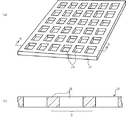
実施の形態1
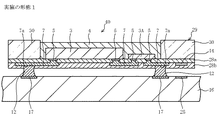
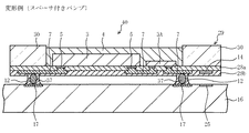
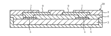
図1は、本実施の形態の半導体装置及びその実装構造の概略断面図を示す。図示の如く、個片化後の半導体装置40は、支持体がガラス基板30で形成され、これに囲まれて複数の異なるチップ部品3、3Aが配され、これらのチップ部品3、3Aの電極5の側以外の面が例えばエポキシ樹脂4で覆われ、このエポキシ樹脂4を介してチップ部品3、3Aがガラス基板30に一体化されている。
FIG. 1 is a schematic cross-sectional view of a semiconductor device and its mounting structure according to the present embodiment. As shown in the figure, the
そして、チップ部品3、3Aの電極5から引き出された配線7が感光性絶縁膜28a、28bの層間に形成され、半導体装置40に設けられたアライメントマーク14がプリント配線板16上のアライメントマーク25に位置合せされた後、はんだ12を介して上記配線7の外部接続端子7aがプリント配線板16の外部接続端子17に接続され、実装された状態である。
The
このように、チップ部品3、3Aの搭載エリアとして、例えばくり貫き加工を行ったガラス基板30等の光透過性材料を支持体材料とし、硬化収縮等による寸法変化が起こり易い材料である樹脂4のエリアを小さくすることにより、寸法安定性のあるMCMを構成できると共に、ガラスを支持体材料とすることにより、光透過型アライメントを利用して位置精度良く実装できる。後述する他の実施の形態も同様。
As described above, as the mounting area for the
図2〜図6によりその製造プロセスを説明する。 The manufacturing process will be described with reference to FIGS.
まず、図2(a)に示すように、従来と同様に仮の基板として例えば石英基板1を用い、その表面の所定位置にチップ部品を搭載するためのアライメントマーク13をプリント配置する。勿論、基板材料としては従来と同様にガラスを用いてもよい。
First, as shown in FIG. 2A, for example, a
次に、図2(b)に示すように、上記のアライメントマーク13を形成した面側の石英基板1上に、チップ部品等の固定材として、例えば紫外線照射により粘着力が低下する粘着シート2を貼り付ける。
Next, as shown in FIG. 2B, on the
次に、図2(c)に示すように、搭載するチップ部品3、3Aの電極5を下向きにし、かつこれらの電極5を石英基板1上のアライメントマーク13に精度良く位置合せして、チップ部品3、3Aを粘着シート2に貼り付ける。なお、これらのチップ部品は予め検査により良品と確認されたものである。
Next, as shown in FIG. 2 (c), the electrodes 5 of the
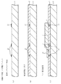
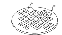
一方、上記したプロセスと平行して、光透過性の支持体となるガラス基板30を図5のように作製する。図5(a)は加工終了後のガラス基板30の概略斜視図、図5(b)は図5(a)のb−b線拡大断面図の一部分を示す。そして図5(b)におけるB部分として図3以降の各図を説明する。
On the other hand, in parallel with the above-described process, a
光透過性の支持体として用いる材料は、耐熱性、機械的強度及び透明性に優れたものである。この材料としては例えば石英等のガラス系材料が好適であり、またポリカーボネート等も使用可能であるが、本実施の形態では青板ガラス(以下、ガラスと称する。)を材料に用い、上記プロセスと平行して、ガラス基板30に所定のパターンでチップ部品搭載エリアをくり貫いた欠除部31の加工を行う。穴加工方法としては、サンドブラスト法やケミカルエッチング法で行うことが可能である。ここで、ガラス基板30は低線膨張で熱変形が小さく、光透過性があることが重要であり、この要件を満たせば、ガラス基板でなくてもよい。
A material used as a light-transmitting support is excellent in heat resistance, mechanical strength, and transparency. As this material, for example, a glass-based material such as quartz is suitable, and polycarbonate or the like can also be used, but in this embodiment, blue plate glass (hereinafter referred to as glass) is used as a material and parallel to the above process. Then, the processing of the
また、くり貫いた欠除部31のサイズは、搭載チップサイズに対して必要最低限の極力小さいサイズ(チップサイズ+0.4mmが目安サイズ)で開口することがポイントであり、これにより後述する充填材の塗布量を少なくすることができ、寸法安定性のあるMCMが達成できる。
In addition, the size of the
また、図6に示すように、ガラス基板30の形状は円形であってもよい。基板が円形であっても、欠如部31は図5に示した方形の基板の場合と同じである。
Moreover, as shown in FIG. 6, the shape of the
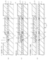
次に、図3(d)に示すように、ガラス基板30に形成した欠除部31の中にチップ部品3、3Aを精度良く位置させて、ガラス基板30と共に粘着シート2に貼り付ける。
Next, as shown in FIG. 3D, the chip components 3, 3 </ b> A are accurately positioned in the
次に、図3(e)に示すように、ガラス基板30の欠除部31に対して、チップ部品3、3Aの電極面以外を覆うように樹脂4を塗布する。この材料としては高フィラー充填のエポキシ樹脂やガラス系の材料を使用する。このように、限られた狭い領域の欠除部31のみに樹脂4を充填することにより、樹脂4の硬化収縮による変形が極めて小さいため、寸法安定性のあるチップ部品3、3Aを形成できると共に、ガラス基板30が疑似ウェーハ29として機能する。
Next, as shown in FIG. 3 (e), the
次に、図3(f)に示すように、石英基板1の裏側から紫外線27を照射して、粘着シート2の粘着力を弱め、疑似ウェーハ29を粘着シート2から剥離する。この場合、紫外線27の照射に代えて、加熱により剥離することもできる。
Next, as shown in FIG. 3 (f), ultraviolet rays 27 are irradiated from the back side of the
次に、図4(g)に示すように、チップ部品3、3Aの電極5が上になるように疑似ウェーハ29をひっくり返す。そして感光性絶縁膜28aを全面に塗布し、しかる後、チップ部品3、3Aの電極5の上部を開口する。この場合、感光性絶縁膜28としては400nm(短波長)で光を吸収する感光性絶縁樹脂をスピンコートし、400nmの光を用いたフォトプロセスで開口し、後述する配線はセミアディティブ法で形成する。
Next, as shown in FIG. 4G, the
即ち、全面にTi/Cu等のシードメタル(図示省略)を形成後、図4(h)に示すように、レジストマスク32を形成してCu電界めっきを行い配線7を形成する。しかる後に、レジストマスク32の除去及びシードメタル膜エッチング(いずれも図示省略)を行う。そして、配線7の形成と同時に、配線7と同じ材料を用いてアライメントマーク14を形成する。
That is, after a seed metal (not shown) such as Ti / Cu is formed on the entire surface, as shown in FIG. 4H, a resist
次に、図4(i)に示すように、上記した感光性絶縁膜28aと同様の感光性絶縁樹脂を全面にスピンコートして感光性絶縁膜28bを形成し、更に上記と同様に400nmの光を用いたフォトプロセスにより、配線7の上部の感光性絶縁膜28bを開口して外部接続端子34を形成する。
Next, as shown in FIG. 4 (i), a photosensitive insulating resin similar to the above-described photosensitive
これにより、400nmの光に感光されていない部分の感光性絶縁膜28aと28bとの層間に存在する形でアライメントマーク14が形成される。従って、透明なガラス基板30に接して感光性絶縁膜28a、28bが設けられ、この感光性絶縁膜28aと28bの中に位置するアライメントマーク14が、後述する位置合せの際に検出し易くなる。
As a result, the
以上のプロセスを経た後に、図4(i)における切断線33の位置で切断する。従って、チップ部品3、3Aは樹脂4で保護されており、ガラス基板30の位置で切断するので、チップ部品3、3Aにはダメージを与えることがなく、個片化後のハンドリングが容易となる。
After passing through the above process, it cut | disconnects in the position of the cutting
このように、チップ部品3、3Aの支持体となる疑似ウェーハ29を光透過性の材料、即ちガラス基板30で形成し、アライメントマーク14を配線7と同一の材料を用いてこの配線7と同時に形成し、このアライメントマーク14の上下に400nmで感光する感光性絶縁膜28a28bを配することによって、光透過性の支持体及び感光性絶縁膜を通してアライメントが可能な光透過型アライメントを利用するのが本実施の形態(後述の実施の形態も同様。)の特長である。
In this way, the
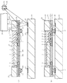
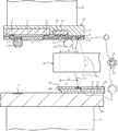
図7は、本実施の形態の実装方法を示す。図示の如く、図18に示した従来の実装方法とは異なり、位置合せ用のカメラ26を実装される半導体装置40のガラス基板30の上方に配置する。なお、本実施の形態においても、実装される半導体装置40は真空チャックで支持され、プリント配線板16も加熱ステージ上等に固定されるが図示省略する。
FIG. 7 shows a mounting method according to the present embodiment. As shown in the figure, unlike the conventional mounting method shown in FIG. 18, the
アライメントマークは従来と同様に十文字状に形成されている。即ち、カメラ26の領域の外側に示したように、半導体装置40のアライメントマーク14よりも一回り大きいマーク25がプリント配線板16に形成されており、カメラ26からの出射光L1が、一つは半導体装置40のアライメントマーク14に当たって反射する反射光L2をなし、他の一つはプリント配線板16のアライメントマーク25に当たって反射する反射光L2となり、これらの反射光L2によって双方のアライメントマーク14、25を光学的に検出して、補正しながら位置合せすることができる。勿論、図18に示した従来と同様な方法で位置合せすることも可能である。
The alignment mark is formed in a cross shape as in the prior art. That is, as shown outside the area of the
図7(j)に示すように、実装に当っては半導体装置40の外部接続端子34にはんだボール12Aを形成し、不図示の真空チャックで半導体装置40を把持し、カメラ26からそれぞれのアライメントマーク14、25に対して光L1を出射してその反射光L2を検出しながら位置合せを行うが、既述したように、チップ部品3、3Aの支持体が透明なガラス基板30からなり、これに接する感光性絶縁膜28a、28bが400nmの短波長の光を吸収する感光性樹脂からなっている。
As shown in FIG. 7 (j), in mounting, the
従って、位置合せ時には、約1μm(103nm)の長波長の赤外光L1をカメラ26から出射することにより、90%以上の透過率にて感光性絶縁膜28a、28bを通して、アライメント14及び15での赤外光L1の反射光L2を検出することができる。しかし、透過率は95〜96%が好ましいため、透過率が十分でない場合は、赤外光L1として更に長波長の光を選ぶか、若しくは感光性絶縁膜28a、28bの界面の調整又は材質の選択により透過率を高めることができる。
Therefore, at the time of alignment, the infrared light L 1 having a long wavelength of about 1 μm (10 3 nm) is emitted from the
更に、本実施の形態は、従来のように位置合せ後にカメラを外すことなしで、双方のアライメントマーク14、25をカメラ26によって位置合せしながら半導体装置40を接近させ、はんだボール12Aをプリント配線板16の外部接続端子17に接触させ、外部接続端子17の表面に配された不図示のはんだペーストにはんだボール12Aが粘着し、仮固定後もカメラ26を用いて位置合せができるため、従来よりも更に精度良く位置合せができる。そして位置合せ終了後は、この状態のプリント配線板16及び半導体装置40は、従来と同様な治具を用いて不図示のリフロー炉に搬入される。
Further, in the present embodiment, the
図7(k)は実装完了の状態を示しており、実装された半導体装置40はリフロー後のはんだ12を介して、半導体装置40の外部接続端子34とプリント配線板16の外部接続端子17とが接続される。
FIG. 7K shows a state where the mounting is completed, and the mounted
本実施の形態によれば、チップ部品3、3Aが樹脂4を介して、ガラス基板30の欠除部31においてこのガラス基板に一体化されているので、樹脂4の領域が小さく形成されるため、硬化収縮による樹脂4の変形は小さいことにより、チップ部品3、3Aの位置精度を保つことができると共に、配線7等の形成も疑似ウェーハレベルで一括処理後に、疑似ウェーハからガラス基板30の位置で切断して個片化できることにより、チップ部品3、3Aが樹脂4で保護され、ガラス基板30に一体化されているため、個片化の際にチップ部品3、3Aがダメージを受けることもなく、個片化後のハンドリングも容易である。
According to the present embodiment, since the
更に、半導体装置40をプリント配線板16上に仮固定した状態で、半導体装置40のアライメントマーク14とプリント配線板16のアライメントマーク25とを、ガラス基板30を通して、カメラ26からの出射光L1の各アライメントマーク14、25での反射光L2を検出し、双方のアライメントマーク14、25を容易かつ高精度に位置合せできるため、半導体装置40をプリント配線板16に対して位置精度良く実装できる。
Further, with the
実施の形態2
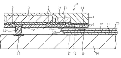
図8(a)は、本実施の形態の半導体装置及びその実装構造の概略断面図、図8(b)は同実施の形態の他の実装構造の概略断面図を示す。
FIG. 8A shows a schematic cross-sectional view of the semiconductor device and its mounting structure of the present embodiment, and FIG. 8B shows a schematic cross-sectional view of another mounting structure of the same embodiment.
本実施の形態においても実施の形態1と同様に、支持体の材料としてガラスを使用していることにより、光学素子(PDやLD)を含むMCMの光実装においても、光透過型アライメントを利用して、半導体装置に形成されたアライメントマークと、光導波路に形成されたアライメントマークを透過アライメントして位置合せしながら、位置精度良くアライメントして実装することができる。 Also in this embodiment, as in the first embodiment, glass is used as the material for the support, so that the light-transmissive alignment is also used in the optical mounting of the MCM including the optical element (PD or LD). Then, the alignment mark formed on the semiconductor device and the alignment mark formed on the optical waveguide can be aligned and mounted with high positional accuracy while being aligned by transmission alignment.
図示の如く、本実施の形態の半導体装置41及び半導体装置41Aも、その基本構造は実施の形態1と同様であり、記述した作製プロセス(図2〜図6参照)により形成されるので、半導体装置41、41Aの作製プロセスの説明は省略する。
As shown in the figure, the basic structure of the
しかし、本実施の形態において配置されているチップ部品が、半導体装置41は半導体チップ3に対して例えばLD(レーザダイオード)又はLED(発光ダイオード)10が配され、半導体装置41Aは半導体チップ3に対して例えばPD(フォトダイオード)23が配され、双方が光導波路20を介して光信号を送受信する平置構造のMCMとして構成されている。
However, the chip component arranged in the present embodiment is such that the
従って、半導体装置41のLD又はLED(以下、LDと称する。)10の発光部11に対向する位置に光導波路20の光入射部20aが配され、入射光が反射面20bで反射し、光導波路20のコア層22内で導波されて反対側の反射面20bで反射し、この反射光が光導波路20の光出射部20cから出射して半導体装置41AのPD23の受光部24に入射するように、この受光部24に対向する位置に光導波路20の光出射部20cが配置されている。
Accordingly, the
このように、半導体装置41、41Aを光導波路20と組み合せたMCM構造においては、各半導体装置41、41Aの光導波路20に対する位置精度は極めて重要であるため、上記した実施の形態1と同様に形成された半導体装置41、41Aのアライメントマーク14と、光導波路20に形成されたアライメントマーク19との正確な位置合せが必要であり、この位置合せが実施の形態1と同様に光透過型アライメントを利用することにより、良好に実施することができる。
As described above, in the MCM structure in which the
図8(a)は、このような構成の半導体装置41、41Aが、はんだ12を介してプリント配線板16の外部接続端子17に対して接続された状態であるが、これと同様な構成の半導体装置41、41Aをメタルポスト43及びはんだバンプ44を介してプリント配線板16の外部接続端子17に接続し、図8(b)のような構造で実装することもできる。いずれも、スペーサ35を介して半導体装置41、41Aとプリント配線板16との距離が100μmに規制されている構造となっている。
FIG. 8A shows a state in which the
図9〜図11によりその実装プロセスを説明する。なお、本実施の形態の半導体装置41、41Aも、チップ部品3、10及び23も樹脂4で保護されており、ガラス基板30の位置で切断されるので、これらのチップ部品がダメージを受けることはなく、個片化後のハンドリングが容易である。
The mounting process will be described with reference to FIGS. In addition, since the
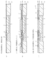
まず、図9(a)は実装基板としてのプリント配線板16及びその外部接続端子17を示し、このプリント配線板16の上面に、図9(b)に示すように光導波路20が不図示の接着剤を介して所定位置に貼り付けられる。なお、図9〜図11においては各部の構造を明示するために、上記した図8における左半分(即ち、半導体装置41側に対応する部分)を図示し、これとほぼ対称的な右半分は図示省略する。
First, FIG. 9A shows a printed
次に、図10(a)に示すように、プリント配線板16上の所定場所にスペーサ35の材料として、熱硬化性樹脂(例えばエポキシ樹脂)を滴下する。図10(b)はこの平面図を示しており、この図において、大小の四角形に仮想線で示す領域30は実装する半導体装置41のガラス基板30の位置を示し、例えば内側の仮想線の角部(4ヶ所)に実線で示す符号35の位置に、図10(a)に示したスペーサ35は滴下されるものであるが、図10(a)においては簡略図示している。なお、このスペーサ35は図10(b)に仮想線にて示したように、例えば3ヶ所に設けてもよい。
Next, as shown in FIG. 10A, a thermosetting resin (for example, epoxy resin) is dropped as a material of the
次は図11(a)に示すように、実装する半導体装置41をこの上方から徐々に近づけ、カメラ26を用いて双方のアライメントマークを位置合せしながら位置合せ終了後にリフロー炉に搬入されるが、実施の形態1と同じ要領で行われるので、同様な位置合せ動作等の説明は省略する。
Next, as shown in FIG. 11 (a), the
しかしこの場合、半導体装置41のアライメントマーク14は実施の形態1と同様に形成されているが、実施の形態1におけるプリント配線板16側のアライメントマークはなく、光導波路20に設けられたアライメントマーク19に対して半導体装置41のアライメントマーク14が位置合せされる。なお、この場合も図18で説明した従来の方法で位置合せすることも可能である。
However, in this case, the
本実施の形態の場合、光導波路20の光入射部20aを通して反射面20bとLDチップ10の発光部11との位置が一致することが最も重要であり、この位置決めの方法としては、従来(図18)と同様に、光導波路20のアライメントマーク19と、この光導波路20の先端側の上面の不図示の光入射部20aとの距離Dと、半導体装置41のアライメントマーク14とLDチップ10の発光部分11との距離Dとは同一であるので、双方のアライメントマーク14と19とを位置合せし、補正しながら実装することにより、LDチップ10の発光部11が自動的に光導波路20の光入射部20aの位置に一致する。
In the case of the present embodiment, it is most important that the positions of the reflecting
従って、光導波路20の光入射部20aから入射するLDチップ10の発光部11の出射光は、光導波路20のコア層22の45°傾斜の反射面20bで反射し、コア層22内を全反射しながら反対側の不図示の半導体装置41A側へ導波される。
Accordingly, the light emitted from the
プリント配線板16に滴下されたスペーサ35となる熱硬化性樹脂は、150〜200℃での数秒で硬化するため、半導体装置41の外部接続端子7aに設けられたはんだボール12Aのリフロー時の熱によっても変形せず、図11(b)に示すように実装を完了するまではスペーサ35として機能する。又、この熱硬化性樹脂はリフロー時のはんだボール12Aのセルフアライメント効果も抑えることにもなり、半導体装置41とプリント配線板16及び光導波路20の上面との距離、及び反射面20bとLDチップ10の発光部11との位置が一定に保たれた状態で、半導体装置41とプリント配線板16とは、はんだ12を介して接続され、不図示の右側の半導体装置41A側も同時にして実装を完了する。
The thermosetting resin that becomes the
本実施の形態によれば、上記した実施の形態1と同様に、チップ部品3、10、23が樹脂4を介して、ガラス基板30の欠除部31においてこのガラス基板30に一体化されているので、樹脂4の領域が小さく形成されるため、硬化収縮による樹脂4の変形は小さくなることにより、チップ部品3、10、23の位置精度を保つことができると共に、配線7等の形成も疑似ウェーハレベルで一括処理後に、疑似ウェーハからガラス基板30の位置で切断して個片化できることにより、チップ部品3、10、23が樹脂4で保護され、ガラス基板30に一体化されているため、個片化の際にチップ部品3、10、23がダメージを受けることもなく、個片化後のハンドリングも容易である。
According to the present embodiment, similarly to the first embodiment described above, the
更に、半導体装置41、41Aをプリント配線板16上に仮固定した状態で、半導体装置41、41Aのアライメントマーク14とプリント配線板16のアライメントマーク19とを、ガラス基板30を通して、カメラ26からの出射光L1の各アライメントマーク14、19での反射光L2を検出し、双方のアライメントマーク14、19を容易かつ高精度に位置合せできるため、半導体装置41、41Aをプリント配線板16に対して位置精度良く実装できる。
Further, with the
図12は、プリント配線板16に複数の半導体装置が実装された状態の一例を示す。上記した実施の形態1による半導体装置40及び実施の形態2による半導体41、41Aは、図示の如く、同一のプリント配線板16上に不図示の他の電子部品等と共に、混載して実装することもできる。
FIG. 12 shows an example of a state in which a plurality of semiconductor devices are mounted on the printed
図13は、上記した実施の形態1による実装構造の変形例を示す。上記した各実施の形態における半導体装置とプリント配線板との接続方法としては、図示の如く、樹脂核37入りのはんだ12を用いてもよい。この場合、リフロー前のはんだボールは、内部に樹脂核37入りのはんだボールの直径を150μm程度とすることにより、リフロー後は半導体装置とプリント配線板との距離を100μmに形成することができる。これは実施の形態2にも適用できる。
FIG. 13 shows a modification of the mounting structure according to the first embodiment. As a method for connecting the semiconductor device and the printed wiring board in each of the above-described embodiments,
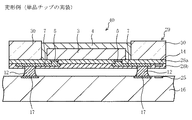
図14は他の変形例を示す。上記した各実施の形態は、種類の異なる複数のチップ部品をワンパッケージ化した半導体装置の実装であるが、図14に示すように、単品のチップ部品の実装にも上記実施の形態は適用することができる。 FIG. 14 shows another modification. Each of the above-described embodiments is mounting of a semiconductor device in which a plurality of different types of chip components are packaged. However, as shown in FIG. 14, the above-described embodiment is also applied to mounting of single-chip components. be able to.
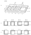
図15は、更に他の変形例を示すものであり、図5及び図6に示したガラス基板30は、一部分または全部を例えば図15に示すガラス基板30aのように作製してもよい。即ち、例えば図5における欠除部31を2個連続したような欠除部31a(図15(a)におけるA1、A2及びB1からB2に亘る領域の欠除部31a)、または図5における欠除部31を4個合せたような欠除部31b(図15(a)におけるC1からC2に亘る領域の欠除部31b)のように形成することもできる。
FIG. 15 shows still another modification, and the
図15(a)において交差する直線の仮想線は切断線50を示し、実施の形態1に説明したプロセス(図3〜図4参照)を経て、この欠除部31a、31bに配したチップ部品を樹脂4で覆った後に、この切断線50で切断して個片化することにより、図15(a)におけるA1、A2、B1、B2領域のA及びB区域では、図15(b)に示すように、3辺がガラス基板30aで囲まれた半導体装置が得られる。
In FIG. 15A, the virtual lines intersecting with each other indicate the cutting
また、図15(a)におけるC1、C2領域のA及びB区域では、図15(c)に示すように、2辺がガラス基板30bで囲まれた半導体装置が得られ、いずれも樹脂4の塗布領域が小さくなることにより、樹脂4の硬化収縮によるチップ部品の位置ずれ等を抑えることができる。
Further, in the areas A 1 and B of the C 1 and C 2 regions in FIG. 15A, as shown in FIG. 15C, a semiconductor device in which two sides are surrounded by a
上記した各実施の形態は、本発明の技術的思想に基づいて種々に変形できる。 Each of the above-described embodiments can be variously modified based on the technical idea of the present invention.
例えば、半導体装置の作製プロセス終了後は、図4(i)に示すように、ガラス基板30の位置で切断し、半導体装置に個片化するとしたが、例えば、図8のように、光導波路20と組み合せて2個の半導体装置41、41Aを隣接して実装するものである場合、光導波路20との寸法関係等の条件が合えば、図5又は図6に示したガラス基板30の隣接した欠除部において、予め半導体装置41、41Aを配設しておくことにより、双方の間で切断することなしに、半導体装置41、41Aを連結して形成でき、連結された半導体装置41、41Aを用いて実装することもできる。また、これに限らず、他の半導体装置40同士でも条件が合えば適用可能である。
For example, after the manufacturing process of the semiconductor device is finished, as shown in FIG. 4 (i), it is cut at the position of the
また、実施の形態に示した各部の構造や形状及び材料等も適宜に変更してもよい。 In addition, the structure, shape, material, and the like of each part described in the embodiment may be changed as appropriate.
1…石英基板、2…粘着シート、3、3A…半導体チップ、4…樹脂、
5…電極パッド、7…配線、7a、17、34…外部接続端子、10…LD又はLED、
11…発光部、12…はんだ、12A…はんだボール、
13、14、19、25…アライメントマーク、16…プリント配線板、
20…光導波路、20a…光入射部、20b…反射面、20c…光出射部、
21…クラッド層、22…コア層、23…FD、24…受光部、26…カメラ、
27…紫外線、28a、28b…感光性絶縁膜、29…疑似ウェーハ、
30…ガラス基板、31…欠除部、32…レジストマスク、33…切断線、
35…スペーサ、37…樹脂核、40、41、41A…半導体装置、
43…メタルポスト、44…はんだバンプ、50…切断線、B…個片領域、D…距離、
L1…出射光、L2…反射光
DESCRIPTION OF
5 ... Electrode pad, 7 ... Wiring, 7a, 17, 34 ... External connection terminal, 10 ... LD or LED,
11 ... light emitting part, 12 ... solder, 12A ... solder ball,
13, 14, 19, 25 ... alignment mark, 16 ... printed wiring board,
20 ... Optical waveguide, 20a ... Light incident part, 20b ... Reflecting surface, 20c ... Light emitting part,
21 ... cladding layer, 22 ... core layer, 23 ... FD, 24 ... light receiving part, 26 ... camera,
27 ... UV light, 28a, 28b ... photosensitive insulating film, 29 ... pseudo wafer,
30 ... Glass substrate, 31 ... Deletion part, 32 ... Resist mask, 33 ... Cutting line,
35 ... spacer, 37 ... resin core, 40, 41, 41A ... semiconductor device,
43 ... Metal post, 44 ... Solder bump, 50 ... Cutting line, B ... Individual area, D ... Distance,
L 1 ... outgoing light, L 2 ... reflected light
Claims (55)
前記チップ部品の側方に設けられた光透過性の支持体に、前記保護物質を介して前記 チップ部品が一体化されていることを特徴とする、半導体装置。 In a semiconductor device constituted by a chip component provided with an electrode on one surface and a protective substance covering at least the side surface other than the electrode surface of the chip component,
A semiconductor device, wherein the chip component is integrated with a light-transmitting support provided on a side of the chip component via the protective substance.
光透過性の材料からなる支持体の近傍位置にチップ部品を配置する工程と、
前記チップ部品の少なくとも側面を覆うようにして前記支持体と前記チップ部品との 間を保護物質で一体化する工程と
を有することを特徴とする、半導体装置の製造方法。 In a method of manufacturing a semiconductor device constituted by a chip component provided with an electrode on one surface and a protective material covering at least a side surface other than the electrode surface of the chip component,
A step of placing a chip component in the vicinity of a support made of a light transmissive material;
And a step of integrating a protective material between the support and the chip component so as to cover at least a side surface of the chip component.
光透過性の材料からなる支持体の近傍位置にチップ部品を配置する工程と、
前記チップ部品の少なくとも側面を覆うようにして前記支持体と前記チップ部品との 間を保護物質で一体化する工程と
によって、前記保護物質で前記チップ部品が前記支持体と一体化されてなる疑似ウェーハを得る、疑似ウェーハの製造方法。 In a manufacturing method of a pseudo wafer used for manufacturing a semiconductor device constituted by a chip component provided with an electrode on one surface and a protective material covering at least a side surface other than the electrode surface of the chip component,
A step of placing a chip component in the vicinity of a support made of a light transmissive material;
The chip component is integrated with the support body with the protective substance by integrating the support body and the chip part with a protective substance so as to cover at least the side surface of the chip part. A pseudo-wafer manufacturing method for obtaining a wafer.
55. The method of mounting a semiconductor device according to claim 54, wherein a thermosetting resin is attached on the circuit board, and the thermosetting resin is cured when the semiconductor device is mounted.
Priority Applications (1)
| Application Number | Priority Date | Filing Date | Title |
|---|---|---|---|
| JP2004105835A JP2005294444A (en) | 2004-03-31 | 2004-03-31 | Semiconductor device and manufacturing method thereof, pseudo wafer and manufacturing method thereof, and mounting structure of semiconductor device and mounting method thereof |
Applications Claiming Priority (1)
| Application Number | Priority Date | Filing Date | Title |
|---|---|---|---|
| JP2004105835A JP2005294444A (en) | 2004-03-31 | 2004-03-31 | Semiconductor device and manufacturing method thereof, pseudo wafer and manufacturing method thereof, and mounting structure of semiconductor device and mounting method thereof |
Publications (1)
| Publication Number | Publication Date |
|---|---|
| JP2005294444A true JP2005294444A (en) | 2005-10-20 |
Family
ID=35327059
Family Applications (1)
| Application Number | Title | Priority Date | Filing Date |
|---|---|---|---|
| JP2004105835A Pending JP2005294444A (en) | 2004-03-31 | 2004-03-31 | Semiconductor device and manufacturing method thereof, pseudo wafer and manufacturing method thereof, and mounting structure of semiconductor device and mounting method thereof |
Country Status (1)
| Country | Link |
|---|---|
| JP (1) | JP2005294444A (en) |
Cited By (10)
| Publication number | Priority date | Publication date | Assignee | Title |
|---|---|---|---|---|
| JP2007155562A (en) * | 2005-12-07 | 2007-06-21 | Acrorad Co Ltd | Radiation image detection module and radiation image detection apparatus |
| JP2007155561A (en) * | 2005-12-07 | 2007-06-21 | Acrorad Co Ltd | Radiological image detection module and radiological image detection device |
| JP2008216794A (en) * | 2007-03-06 | 2008-09-18 | Furukawa Electric Co Ltd:The | Optical coupler |
| JP2010105153A (en) * | 2008-10-28 | 2010-05-13 | Honeywell Internatl Inc | Mems device and method for assembling microelectromechanical system (mems) |
| JP2011176297A (en) * | 2010-01-27 | 2011-09-08 | Ricoh Co Ltd | Imaging module, method of manufacturing the same, and imaging device |
| JP2012188555A (en) * | 2011-03-10 | 2012-10-04 | Sumitomo Bakelite Co Ltd | Semiconductor device and method of manufacturing semiconductor device |
| WO2013042364A1 (en) * | 2011-09-20 | 2013-03-28 | 日本電気株式会社 | Optical transmission module |
| JP2014089394A (en) * | 2012-10-31 | 2014-05-15 | Kyocera Corp | Optical device substrate and optical device |
| JP2016092220A (en) * | 2014-11-05 | 2016-05-23 | 日立化成株式会社 | Silicon-containing substrate, semiconductor device using the same and semiconductor device manufacturing method |
| JP2020166189A (en) * | 2019-03-29 | 2020-10-08 | 日東電工株式会社 | Optical-electric mixed board with optical element and its manufacturing method |
-
2004
- 2004-03-31 JP JP2004105835A patent/JP2005294444A/en active Pending
Cited By (11)
| Publication number | Priority date | Publication date | Assignee | Title |
|---|---|---|---|---|
| JP2007155562A (en) * | 2005-12-07 | 2007-06-21 | Acrorad Co Ltd | Radiation image detection module and radiation image detection apparatus |
| JP2007155561A (en) * | 2005-12-07 | 2007-06-21 | Acrorad Co Ltd | Radiological image detection module and radiological image detection device |
| JP2008216794A (en) * | 2007-03-06 | 2008-09-18 | Furukawa Electric Co Ltd:The | Optical coupler |
| JP2010105153A (en) * | 2008-10-28 | 2010-05-13 | Honeywell Internatl Inc | Mems device and method for assembling microelectromechanical system (mems) |
| JP2011176297A (en) * | 2010-01-27 | 2011-09-08 | Ricoh Co Ltd | Imaging module, method of manufacturing the same, and imaging device |
| JP2012188555A (en) * | 2011-03-10 | 2012-10-04 | Sumitomo Bakelite Co Ltd | Semiconductor device and method of manufacturing semiconductor device |
| WO2013042364A1 (en) * | 2011-09-20 | 2013-03-28 | 日本電気株式会社 | Optical transmission module |
| JP2014089394A (en) * | 2012-10-31 | 2014-05-15 | Kyocera Corp | Optical device substrate and optical device |
| JP2016092220A (en) * | 2014-11-05 | 2016-05-23 | 日立化成株式会社 | Silicon-containing substrate, semiconductor device using the same and semiconductor device manufacturing method |
| JP2020166189A (en) * | 2019-03-29 | 2020-10-08 | 日東電工株式会社 | Optical-electric mixed board with optical element and its manufacturing method |
| JP7408292B2 (en) | 2019-03-29 | 2024-01-05 | 日東電工株式会社 | Optical-electrical hybrid board with optical element and manufacturing method thereof |
Similar Documents
| Publication | Publication Date | Title |
|---|---|---|
| USRE41369E1 (en) | Semiconductor device and method of manufacturing the same | |
| TWI353045B (en) | ||
| US7534656B2 (en) | Image sensor device and method of manufacturing the same | |
| KR100657117B1 (en) | Integrated circuit device and method for manufacturing the same | |
| US4862249A (en) | Packaging system for stacking integrated circuits | |
| US5138145A (en) | Method for producing image sensors with current flow into chip and with simplified chip mounting | |
| JP6395600B2 (en) | Imaging device manufacturing method and semiconductor device manufacturing method | |
| US7457490B2 (en) | Micro-optics on optoelectronics | |
| CN1568546B (en) | Semiconductor device and manufacturing method thereof | |
| US7443028B2 (en) | Imaging module and method for forming the same | |
| US20080191335A1 (en) | Cmos image sensor chip scale package with die receiving opening and method of the same | |
| JP2005033141A (en) | Semiconductor device and manufacturing method thereof, pseudo wafer and manufacturing method thereof, and mounting structure of semiconductor device | |
| JP2002368160A (en) | Wafer level package and manufacturing method thereof | |
| TW201405764A (en) | Wafer stack assembly | |
| CN107808887A (en) | Optical device and method for manufacturing the same | |
| EP1251557B1 (en) | Method of manufacturing semiconductor devices and semiconductor device | |
| US7615408B2 (en) | Method of manufacturing semiconductor device | |
| JP2005294444A (en) | Semiconductor device and manufacturing method thereof, pseudo wafer and manufacturing method thereof, and mounting structure of semiconductor device and mounting method thereof | |
| JP2004363279A (en) | Method of manufacturing photoelectric conversion device, and method of manufacturing pseudo wafer used for manufacturing the same | |
| JP2004342862A (en) | Semiconductor device and its manufacturing method, pseudo wafer and its manufacturing method, and multi-chip module | |
| US7391576B2 (en) | Manufacturing of optical units for semiconductor packages with optical sensors | |
| JP4234270B2 (en) | Manufacturing method of semiconductor device | |
| JP4020618B2 (en) | Semiconductor device and manufacturing method thereof | |
| JP2003197659A (en) | Chip-shaped electronic component and manufacturing method thereof, pseudo wafer used for manufacturing the same, and manufacturing method thereof | |
| JP2574559B2 (en) | Image sensor manufacturing method |