JP4903434B2 - Trench cut type light emitting diode and method of manufacturing the same - Google Patents
Trench cut type light emitting diode and method of manufacturing the same Download PDFInfo
- Publication number
- JP4903434B2 JP4903434B2 JP2005505523A JP2005505523A JP4903434B2 JP 4903434 B2 JP4903434 B2 JP 4903434B2 JP 2005505523 A JP2005505523 A JP 2005505523A JP 2005505523 A JP2005505523 A JP 2005505523A JP 4903434 B2 JP4903434 B2 JP 4903434B2
- Authority
- JP
- Japan
- Prior art keywords
- substrate
- trench
- forming
- layer
- device portion
- Prior art date
- Legal status (The legal status is an assumption and is not a legal conclusion. Google has not performed a legal analysis and makes no representation as to the accuracy of the status listed.)
- Expired - Lifetime
Links
Images


Classifications
-
- H—ELECTRICITY
- H01—ELECTRIC ELEMENTS
- H01L—SEMICONDUCTOR DEVICES NOT COVERED BY CLASS H10
- H01L33/00—Semiconductor devices with at least one potential-jump barrier or surface barrier specially adapted for light emission; Processes or apparatus specially adapted for the manufacture or treatment thereof or of parts thereof; Details thereof
- H01L33/02—Semiconductor devices with at least one potential-jump barrier or surface barrier specially adapted for light emission; Processes or apparatus specially adapted for the manufacture or treatment thereof or of parts thereof; Details thereof characterised by the semiconductor bodies
- H01L33/20—Semiconductor devices with at least one potential-jump barrier or surface barrier specially adapted for light emission; Processes or apparatus specially adapted for the manufacture or treatment thereof or of parts thereof; Details thereof characterised by the semiconductor bodies with a particular shape, e.g. curved or truncated substrate
-
- H—ELECTRICITY
- H01—ELECTRIC ELEMENTS
- H01L—SEMICONDUCTOR DEVICES NOT COVERED BY CLASS H10
- H01L33/00—Semiconductor devices with at least one potential-jump barrier or surface barrier specially adapted for light emission; Processes or apparatus specially adapted for the manufacture or treatment thereof or of parts thereof; Details thereof
- H01L33/02—Semiconductor devices with at least one potential-jump barrier or surface barrier specially adapted for light emission; Processes or apparatus specially adapted for the manufacture or treatment thereof or of parts thereof; Details thereof characterised by the semiconductor bodies
-
- H—ELECTRICITY
- H01—ELECTRIC ELEMENTS
- H01L—SEMICONDUCTOR DEVICES NOT COVERED BY CLASS H10
- H01L2224/00—Indexing scheme for arrangements for connecting or disconnecting semiconductor or solid-state bodies and methods related thereto as covered by H01L24/00
- H01L2224/01—Means for bonding being attached to, or being formed on, the surface to be connected, e.g. chip-to-package, die-attach, "first-level" interconnects; Manufacturing methods related thereto
- H01L2224/42—Wire connectors; Manufacturing methods related thereto
- H01L2224/47—Structure, shape, material or disposition of the wire connectors after the connecting process
- H01L2224/48—Structure, shape, material or disposition of the wire connectors after the connecting process of an individual wire connector
- H01L2224/484—Connecting portions
- H01L2224/48463—Connecting portions the connecting portion on the bonding area of the semiconductor or solid-state body being a ball bond
-
- H—ELECTRICITY
- H01—ELECTRIC ELEMENTS
- H01L—SEMICONDUCTOR DEVICES NOT COVERED BY CLASS H10
- H01L2224/00—Indexing scheme for arrangements for connecting or disconnecting semiconductor or solid-state bodies and methods related thereto as covered by H01L24/00
- H01L2224/73—Means for bonding being of different types provided for in two or more of groups H01L2224/10, H01L2224/18, H01L2224/26, H01L2224/34, H01L2224/42, H01L2224/50, H01L2224/63, H01L2224/71
- H01L2224/732—Location after the connecting process
- H01L2224/73251—Location after the connecting process on different surfaces
- H01L2224/73265—Layer and wire connectors
-
- H—ELECTRICITY
- H01—ELECTRIC ELEMENTS
- H01L—SEMICONDUCTOR DEVICES NOT COVERED BY CLASS H10
- H01L33/00—Semiconductor devices with at least one potential-jump barrier or surface barrier specially adapted for light emission; Processes or apparatus specially adapted for the manufacture or treatment thereof or of parts thereof; Details thereof
- H01L33/005—Processes
- H01L33/0095—Post-treatment of devices, e.g. annealing, recrystallisation or short-circuit elimination
Landscapes
- Engineering & Computer Science (AREA)
- Manufacturing & Machinery (AREA)
- Computer Hardware Design (AREA)
- Microelectronics & Electronic Packaging (AREA)
- Power Engineering (AREA)
- Led Devices (AREA)
- Led Device Packages (AREA)
- Semiconductor Lasers (AREA)
Description
本発明は、マイクロ電子工学によるデバイスとその製造方法に関し、より詳細には、発光ダイオード(LED)などの半導体デバイスで用いることができる構造に関する。 The present invention relates to microelectronic devices and methods of manufacturing the same, and more particularly to structures that can be used in semiconductor devices such as light emitting diodes (LEDs).
本出願は、参照によりその開示全体が本明細書に組み込まれて、2002年7月19日に出願した米国仮出願第60/397,488号および2002年10月3日に出願した米国仮出願第60/415,898号に基づく優先権を主張するものである。 This application is incorporated herein by reference in its entirety, US Provisional Application No. 60 / 397,488 filed July 19, 2002 and US Provisional Application filed October 3, 2002. Claims priority based on 60 / 415,898.
発光ダイオードは、消費者向けおよび商業用途に広く用いられている。当業者にはよく知られているように、発光ダイオードは、一般にマイクロ電子工学による基板上のダイオード領域を含む。このマイクロ電子工学による基板には、例えば、ゲルマニウムアルセナイド、リン化ガリウム、それらの合金、炭化ケイ素および/またはサファイアを備えることができる。LEDの絶え間ない開発により、可視スペクトルおよび可視域を超えるスペクトルを網羅する非常に効率的で機械的に強固な光源が得られた。これらの特性により、固体素子の潜在的な高耐用性と相俟って、様々な新しい表示用途が可能となり、LEDは概して広範囲に使用されている白熱灯と競合するようになるだろう。 Light emitting diodes are widely used in consumer and commercial applications. As is well known to those skilled in the art, light emitting diodes generally include a diode region on a substrate by microelectronics. The microelectronic substrate can comprise, for example, germanium arsenide, gallium phosphide, alloys thereof, silicon carbide and / or sapphire. The constant development of LEDs has resulted in a very efficient and mechanically robust light source that covers the visible spectrum and beyond the visible spectrum. These characteristics, coupled with the potential high durability of solid state devices, will allow a variety of new display applications, and LEDs will generally compete with the widely used incandescent lamps.
GaNから成る発光ダイオード(LED)は一般に、複数のGaNベースエピタキシャル層が堆積されるサファイアまたはSiCなどの絶縁性基板、半導体基板または導電性基板を備える。エピタキシャル層は、励起されると光を放出するp−n接合部を有する活性領域を備える。代表的なLEDは、パッケージまたはリードフレームとも呼ばれるサブマウント(以下、「サブマウント(submount)」と呼ぶ)上に基板側を下にして実装される。図1は、n型SiC基板10、基板上に成長しメサ内にパターンを形成したn型−GaNベース層14およびp型−GaNベース層16を含む活性領域12を備えた従来のLEDを概略的に示す図である。金属のp電極18がp型−GaNベース層16上に堆積されてこの層と電気的に結合し、p電極18上のボンドパッド20にワイヤボンドによる接続28がなされている。導電性基板の上にあってこの基板と電気的に結合しているn電極22が、導電性エポキシ樹脂26を使用して金属製サブマウント(metallic submount)24に取り付けられている。従来の製造法では、導電性エポキシ樹脂26(通常は銀エポキシ樹脂)をサブマウント上に堆積させ、LEDがエポキシ樹脂26内に押し込まれる。エポキシ樹脂はその後、硬化を引き起こす熱硬化処理が施され、LEDチップに安定した、かつ電導性の実装が可能となる。活性領域12で発生した光は、デバイスの外、上方に向けられる。しかしながら、発生した光のかなりの量を基板内に伝え、一部はエポキシ樹脂26により吸収される場合がある。
A light emitting diode (LED) made of GaN generally comprises an insulating substrate such as sapphire or SiC, a semiconductor substrate or a conductive substrate on which a plurality of GaN-based epitaxial layers are deposited. The epitaxial layer comprises an active region having a pn junction that emits light when excited. A typical LED is mounted on a submount also called a package or a lead frame (hereinafter referred to as “submount”) with the substrate side facing down. FIG. 1 schematically illustrates a conventional LED comprising an n-
LEDのフリップチップ実装には、サブマウント上に基板側を上にするLEDの実装が含まれる。次に光が取り出され、透明基板を通過して放射される。フリップチップ実装は、SiCから成るLEDを実装するためには特に好ましい手法であろう。SiCは、GaNより屈折率が高いので、活性領域12で発生する光は、GaN/SiC境界面において内部反射(すなわち、GaNから成る層内に戻ること)をしない。SiCベースLEDのフリップチップ実装は、従来技術として知られる特定のチップ成形方法を用いるときに、光の取り出しを改善することができる。SiCから成るLEDのフリップチップのパッケージングには、チップの特定の用途によっては望ましい熱の抽出/放散の改善などの、他の利点もある。
LED flip-chip mounting includes LED mounting with the substrate side up on the submount. The light is then extracted and emitted through the transparent substrate. Flip chip mounting would be a particularly preferred technique for mounting LEDs made of SiC. Since SiC has a higher refractive index than GaN, the light generated in the
図2に、フリップチップ実装に関する問題の1つを示す。すなわち、チップが導電性サブマウントまたはパッケージ上にフリップチップで実装される場合、従来の手法を使用できない可能性がある。従来は、銀エポキシ樹脂などの導電性素子取り付け材料26をチップ上および/またはサブマウント24上に付着させ、このチップをサブマウント24の上に押し付ける。この手法では、粘性のある導電性素子取り付け材料26が押し出され、デバイス内のn型層14と10との接触を引き起こし、これによって予測通りに望ましくない結果を含んだ活性領域内のp−n接合を分流するショットキーダイオード接続(Schottky diode connection)が形成される。
FIG. 2 illustrates one of the problems associated with flip chip mounting. That is, if the chip is mounted on a conductive submount or package in a flip chip, conventional techniques may not be used. Conventionally, a conductive
LED素子(die)が切断加工(sawing)および切断処理によりウェーハから個片切断される(singulated)場合は、切断時に素子の面にかかる応力から別の問題が生じる可能性がある。この応力は、チップ端部の割れを引き起こす可能性がある。この割れがひどいと素子が破壊される可能性がある。例えば、割れがデバイスの活性領域内まで伸長した場合、デバイスが破壊される可能性がある。 When the LED element (die) is singulated from a wafer by a cutting process and a cutting process, another problem may arise from the stress applied to the surface of the element at the time of cutting. This stress can cause chip edge cracks. If this crack is severe, the device may be destroyed. For example, if a crack extends into the active area of the device, the device can be destroyed.
本発明の態様により、デバイスの基板のエピタキシャル層側からその基板内に伸びるトレンチを有する発光素子および発光ダイオードの製造方法が提供される。このトレンチは、個々のデバイスの範囲を定めるメサの周囲に配置され、発光素子の個片切断を行うためにウェーハが切断される領域に配置される。本発明の実施形態では、トレンチの露出部分上にパッシベーション層が設けられる場合もある。メサ分離トレンチにより範囲が定められる活性領域を有する本発明の実施形態では、メサ分離トレンチ内部に第2のトレンチが設けられ、この第2のトレンチはデバイスの基板内に伸び、基板が切断されてウェーハから素子を分ける基板の領域近くに配置することができる。 Aspects of the present invention provide a light emitting device having a trench extending into the substrate from the epitaxial layer side of the device substrate and a method for manufacturing the light emitting diode. The trenches are arranged around mesas that define individual devices, and are arranged in regions where the wafer is cut to cut individual pieces of light emitting elements. In the embodiment of the present invention, a passivation layer may be provided on the exposed portion of the trench. In an embodiment of the invention having an active region delimited by a mesa isolation trench, a second trench is provided within the mesa isolation trench, which extends into the device substrate and the substrate is cut. It can be placed near the area of the substrate that separates the device from the wafer.
本発明の方法の態様では、相対向する第1および第2の面を有する半導体基板と、第1および第2のデバイス部を含む、上記基板の第2の面上の少なくとも1つのデバイス層とを使用する半導体デバイスを形成する方法が提供される。上記基板の第1の面の上記第1のデバイス部と第2のデバイス部との間の位置に第1のトレンチが形成される。上記基板の第2の面の上記第1のデバイス部と第2のデバイス部との間に第2のトレンチが形成される。 In a method aspect of the present invention, a semiconductor substrate having first and second opposing surfaces, and at least one device layer on the second surface of the substrate, including first and second device portions, A method of forming a semiconductor device using the method is provided. A first trench is formed at a position between the first device portion and the second device portion on the first surface of the substrate. A second trench is formed between the first device portion and the second device portion on the second surface of the substrate.
本発明の別の方法の態様では、デバイス面を有する半導体基板と、第1および第2のデバイス部を含む、上記基板のデバイス面上の少なくとも1つのデバイス層とを使用する半導体デバイスを形成する方法が提供される。分離トレンチが、上記少なくとも1つのデバイス層内に形成され、上記第1のデバイス部を含む第1のメサおよび上記第2のデバイス部を含む第2のメサの範囲を定める。第2のトレンチが、上記分離トレンチに沿って上記基板のデバイス面に形成される。上記第2のトレンチは上記第1のデバイス部と第2のデバイス部との間に伸びている。 In another method aspect of the present invention, a semiconductor device is formed using a semiconductor substrate having a device surface and at least one device layer on the device surface of the substrate including first and second device portions. A method is provided. An isolation trench is formed in the at least one device layer and defines a first mesa that includes the first device portion and a second mesa that includes the second device portion. A second trench is formed in the device surface of the substrate along the isolation trench. The second trench extends between the first device portion and the second device portion.
本発明の態様では、半導体基板部材が、相対向する第1および第2の面を有する半導体基板と上記基板の第2の面上の少なくとも1つのデバイス層とを含む。上記少なくとも1つのデバイス層は第1および第2のデバイス部を含む。第1のトレンチが上記基板の第1の面の上記第1のデバイス部と第2のデバイス部との間の位置に範囲を定められている。第2のトレンチが上記第1のデバイス部と第2のデバイス部との間の上記基板の第2の面に範囲を定められている。 In an aspect of the invention, a semiconductor substrate member includes a semiconductor substrate having first and second opposing surfaces and at least one device layer on the second surface of the substrate. The at least one device layer includes first and second device portions. A first trench is delimited at a position between the first device portion and the second device portion of the first surface of the substrate. A second trench is defined in the second surface of the substrate between the first device portion and the second device portion.
本発明の態様では、半導体基板部材が、デバイス面を有する半導体基板と上記基板のデバイス面上の少なくとも1つのデバイス層とを含む。上記少なくとも1つのデバイス層は第1および第2のデバイス部を含む。分離トレンチが上記少なくとも1つのデバイス層内に範囲を定められている。上記分離トレンチは、上記第1のデバイス部を含む第1のメサおよび上記第2のデバイス部を含む第2のメサの範囲を定めている。第2のトレンチが上記分離トレンチの内部およびこれに沿った部分の上記基板のデバイス面内に範囲を定められている。上記定められた第2のトレンチは、上記第1のデバイス部と第2のデバイス部との間に伸びる。 In an aspect of the invention, a semiconductor substrate member includes a semiconductor substrate having a device surface and at least one device layer on the device surface of the substrate. The at least one device layer includes first and second device portions. An isolation trench is delimited within the at least one device layer. The isolation trench defines a range of a first mesa that includes the first device portion and a second mesa that includes the second device portion. A second trench is delimited within the isolation trench and within the device plane of the substrate along the portion. The defined second trench extends between the first device portion and the second device portion.
本発明の目的は、以下に続く好ましい実施形態の図面と本発明を専ら解説するものである詳細な説明とを読むことにより当業者によって理解されるであろう。 Objects of the present invention will be understood by those of ordinary skill in the art upon reading the following detailed description of the preferred embodiment drawings and the detailed description which exclusively describes the invention.
本発明の別の特徴は、下記の本発明の特定の実施形態の詳細な説明を添付の図面を参照して読めばより容易に理解されるであろう。 Other features of the present invention will be more readily understood by reading the following detailed description of specific embodiments of the invention with reference to the accompanying drawings.
本発明について、以下に本発明の実施形態が示されている添付図面を参照し、より十分な説明を行う。しかし本発明は、多くの異なった形で実施することができ、本明細書に記載された実施形態に限定されるものと解釈されるべきではない。むしろ、これらの実施形態を、この開示が完璧で完全なものとし、当業者に本発明の範囲を十分に伝達するために提供する。同じ参照符号は全体を通して同一の構成部品を指す。また、種々の層および領域を図に概略的に示す。当業者により同様に理解されるように、本明細書で基板もしくはその他の層「上に」形成された層に言及する場合は、基板もしくはその他の層上、または基板もしくはその他の層上に形成された介在層もしくはその他の層上に直接形成された層を指す。したがって、本発明は、添付図に示された相対的な大きさや間隔に限定されない。 The present invention will be described more fully hereinafter with reference to the accompanying drawings, in which embodiments of the invention are shown. The present invention may, however, be embodied in many different forms and should not be construed as limited to the embodiments set forth herein; Rather, these embodiments are provided so that this disclosure will be thorough and complete, and will fully convey the scope of the invention to those skilled in the art. Like reference numerals refer to like parts throughout. Also, the various layers and regions are shown schematically in the figure. As will be appreciated by those skilled in the art, references herein to a layer formed “on” a substrate or other layer are formed on the substrate or other layer, or on the substrate or other layer. It refers to a layer formed directly on the intervening layer or other layer formed. Therefore, the present invention is not limited to the relative sizes and intervals shown in the attached drawings.
本発明の実施形態は、例えば、成形基板を有しおよび/またはフリップチップ実装に好適な発光素子などの発光素子を提供するものである。この発光素子は、デバイスの活性領域(例えば、デバイスの「エピタキシャル層」側)が形成され、デバイスの成形基板側と反対側にある表面からデバイスの基板内に伸びるトレンチを有している。このエピタキシャル層側のトレンチにより、応力を逃がし、またはウェーハの切断を容易にする段差を得られ、このためデバイスの接合部内に広がる切断の伝播による歩留まり損失を低減することができる。加えて、フリップチップ実装デバイスに対し、エピタキシャル層側のトレンチは、絶縁性のパッシベーション物質がトレンチカット後のウェーハ上に被着し、このパッシベーション物質でトレンチカットのまわりを効率的に包むことを可能にする。それゆえ、素子取り付け中に素子取り付け材料(例えば、はんだ)がSiC基板と接触し、その結果デバイスのp−n接合間に短絡し、または分流するのを防止する絶縁性バリアを設けることができる。 Embodiments of the present invention provide, for example, a light emitting device such as a light emitting device having a molded substrate and / or suitable for flip chip mounting. The light emitting element has an active region of the device (eg, the “epitaxial layer” side of the device) and has a trench extending into the device substrate from the surface opposite the molded substrate side of the device. This trench on the epitaxial layer side provides a step that relieves stress or facilitates the cutting of the wafer, thus reducing yield loss due to the propagation of the cut spreading into the device junction. In addition, for flip-chip mounted devices, the trench on the epitaxial layer side allows an insulating passivation material to be deposited on the wafer after the trench cut, and this passivation material efficiently wraps around the trench cut. To. Therefore, an insulating barrier can be provided that prevents element attachment material (eg, solder) from contacting the SiC substrate during element attachment and consequently shorting or shunting between the pn junctions of the device. .
上記のように、本発明の特定の実施形態において、発光素子は成形基板を有することがある。SiCは屈折率が高いので、SiC基板を通過する光は、極めて小さな入射角(垂直線にかなり近い角度)で境界面に当たらない限り、その基板の表面において内部の基板内へ全体的に反射される傾向がある。全反射の臨界角は、SiC基板との境界面を形成する材料によって変わってくる。より多くの光線を小さな入射角でSiCの表面に当てることにより全反射を抑えるようにSiC基板を成形することによって、SiCベースLEDからの光出力を増加させることが可能である。このようなチップ成形方法の1つおよびこれによって得られたチップは、特許文献1に示される。 As mentioned above, in certain embodiments of the present invention, the light emitting device may have a molded substrate. Since SiC has a high refractive index, light passing through the SiC substrate is totally reflected into the inner substrate at the surface of the substrate, unless it hits the interface at a very small angle of incidence (an angle very close to the normal). Tend to be. The critical angle of total reflection varies depending on the material forming the interface with the SiC substrate. It is possible to increase the light output from the SiC-based LED by shaping the SiC substrate so as to suppress total reflection by applying more light rays to the surface of the SiC at a small incident angle. One such chip forming method and the chip obtained thereby are disclosed in Patent Document 1.
図3に、個片切断前の上記特許文献1に記載の成形基板を有するLEDチップを示す。詳細には、ウェーハ100は、SiC基板のような基板120を含む図3に示すようなLEDチップ110を含んでいる。LEDチップ110の活性素子領域122は、GaNから成る層などの第III族窒化物を含んでいる。この活性素子領域122および基板120上にコンタクト124および128が設けられている。任意選択で共晶金属(eutectic metal)領域126を設けることもできる。
In FIG. 3, the LED chip which has the shaping | molding board | substrate of the said patent document 1 before piece cutting is shown. Specifically, the
活性領域122は、分離トレンチ132によってメサ内に形成される。この分離トレンチ132は、個々のデバイスまたはいくつかのデバイスの組の範囲を定める役割を果たす。また、分離トレンチ132は、デバイスを分離し、およびいくつかの実施形態では所望の形の基板を提供するために用いられる基板120の成形トレンチ(またはカット)すなわち「ストリート(street)」136と位置が概ね揃えられる。さらに図3に示すように、第2のトレンチ134もまた基板120内に形成される。この第2のトレンチ134は、同様に基板120のストリート136と位置が概ね揃えられ、いくつかの実施形態では、活性領域122のメサ末端を形成する分離トレンチ132内部に形成される。
The
第2のトレンチ134は、分離トレンチ132の形成とは別の製造工程で設けることができ、または同一の工程で形成することもできる。例えば、第2のトレンチ134は、ダイスで加工する、切断加工する、エッチングする、ウォータージェットで切断する、レーザスクライブを行う、または標準的な硬質材料半導体の分離法もしくは個片切断法などのその他の方法を用いて作成することができる。
The
本発明の実施形態では、第2のトレンチ134は、活性領域122内への切断の伝播を低減するように、応力を逃がし、および/または個片切断工程で基板を切断することを容易にするのに十分な長さだけ基板120内に伸ばされる場合がある。例えば、本発明の実施形態において、第2のトレンチ134を基板120内に少なくとも約2μm伸ばす場合がある。他の実施形態では、第2のトレンチ134は、基板120内に少なくとも約5μm伸ばされる。本発明の別の実施形態では、第2のトレンチ134は、基板120内に少なくとも約10μm伸ばされる。本発明の特別な実施形態では、第2のトレンチ134は、基板120内に少なくとも約20μm伸ばされる。いくつかの好ましい実施形態によれば、第2のトレンチ134は、約2μmから5μmの深さで基板120内に伸ばされる。いくつかの実施形態によれば、基板120内の第2のトレンチ134の深さは、基板120の厚さの少なくとも1%である。いくつかの好ましい実施形態によれば、基板120内の第2のトレンチ134の深さは、基板120の約5%から20%である。
In an embodiment of the invention, the
さらに、第2のトレンチ134は、応力を逃がし、および/または活性領域122内への切断が伝播するのを低減するように個片切断工程での基板の切断を容易にすることもできる。本発明の様々な実施形態において、活性領域122として発光素子構造を設けてもよい。例えば、本発明の実施形態によっては、第2のトレンチ134は、少なくとも約2μmの幅を有する。他の実施形態では、第2のトレンチ134は、少なくとも約5μmの幅を有する。本発明の別の実施形態では、第2のトレンチ134は、少なくとも約10μmの幅を有する。本発明の特別な実施形態では、第2のトレンチ134は、少なくとも約25μmの幅を有する。いくつかの好ましい実施形態によれば、第2のトレンチ134は、約2μmから25μmの幅を有する。
In addition, the
いくつかの実施形態によれば、分離トレンチ132は、少なくとも約1μmの深さを有する。いくつかの好ましい実施形態によれば、分離トレンチ132は、2μmから4μmの深さを有する。
According to some embodiments, the
いくつかの実施形態によれば、分離トレンチ132は、少なくとも30μmの幅を有する。いくつかの好ましい実施形態によれば、分離トレンチ132は、約50μmから70μmの幅を有する。
According to some embodiments, the
いくつかの実施形態によれば、成形トレンチ136は、基板120内に少なくとも100μmの深さを有する。いくつかの好ましい実施形態によれば、成形トレンチ136は、基板内に約200μmから220μmの深さを有する。
According to some embodiments, the shaped
いくつかの実施形態によれば、成形トレンチ136は、少なくとも50μmの幅を有する。いくつかの好ましい実施形態によれば、成形トレンチ136は、約75μmから125μmの幅を有する。
According to some embodiments, the shaped
いくつかの好ましい実施形態によれば、成形トレンチ136が基板120内に約150μmから200μmの深さを有した状態で、第2のトレンチ134は、基板120内に約2μmから5μmの深さを有する。いくつかの実施形態によれば、基板120内の第2のトレンチ134の深さは、成形トレンチ136の深さの約5%から10%である。いくつかの実施形態によれば、第2のトレンチ134と成形トレンチ136の間に残っている基板120の厚さは、基板120の元の厚さの少なくとも5%である。いくつかの実施形態によれば、第2のトレンチ134と成形トレンチ136の間に残っている基板120の厚さは、基板120の元の厚さの約5%から15%である。
According to some preferred embodiments, with the shaped
さらに図3に示すように、分離トレンチ132および第2のトレンチ134により露出された表面上に酸化物、窒化物および/または酸窒化物(oxynitride)などのパッシベーション層130を形成することができる。したがって、このパッシベーション層130は、第2のトレンチ134の深さに対応した長さだけ基板120内に伸ばすことができる。本発明の特別な実施形態において、パッシベーション物質は、窒化珪素(SiN)、ドープし、またはドープしない二酸化珪素(SiO2)、シリコン酸窒化物(SiOxNy)、塗布ガラス(Spin−on Glass)、ポリイミド、またはその他任意の絶縁材料もしくは膜の組み合わせが可能であり、化学蒸着法(CVD)、低圧CVD法(LPCVD)、プラズマCVD(PECVD)、スパッタリング、または後に硬化工程が続く未硬化液体のスピン−オン投与(spin−on dispense)により堆積させることができる。
Further, as shown in FIG. 3, a
基板内にパッシベーション層130を形成することにより、活性領域122内のp−n接合まわりの素子取り付け材料のウィッキングによるLED部材の短絡または分流を防止することができる。したがって、第2のトレンチ134の形成後に形成されたパッシベーション層130を有する本発明の実施形態では、第2のトレンチ134の深さは、デバイス110を実装する場合、寄生性のあるショットキーダイオード(parasitic Schottky diode)が生成される可能性を低減するように選択することもできる。
By forming the
本発明の特定の実施形態では、活性領域122は、ノースカロライナ州ダラム市のCree社が製造、販売しているデバイスのような炭化珪素基板上に製造された窒化ガリウムから成るLEDまたはレーザにすることができる。例えば、本発明は、その開示が参照によりあたかも本明細書に完全に記載されたように本明細書に組み込まれる米国特許に記載されたようなLEDおよび/またはレーザで使用するのに適している場合がある(特許文献2、3、4、5、6、7、8、9、10、11、12、13、14、14、15および/または16参照)。その他の好適なLEDおよび/またはレーザが、その開示により本明細書に組み込まれている米国特許に記載されている(特許文献17、18、19、20、ならびに21および1参照)。
In a particular embodiment of the present invention, the
本発明の特定の実施形態において、発光素子は、活性領域で発生した光がデバイスを透過し、反射して戻る反射層を形成するP電極を含んでもよい。反射性のP電極および関連した構造が、参照により本明細書に組み込まれる米国特許に記載されている(特許文献1参照)。 In certain embodiments of the present invention, the light emitting device may include a P electrode that forms a reflective layer in which light generated in the active region is transmitted through the device and reflected back. Reflective P-electrodes and related structures are described in U.S. Patents, which are incorporated herein by reference (see U.S. Pat. No. 6,057,049).
LEDおよび/またはレーザは、基板を透過し、発光が起こるように「フリップチップ」構成で動作するように構成することができる。このような実施形態では、デバイスの光出力を高めるように基板にパターンを形成することができる(例えば、特許文献23および1参照。)。 The LEDs and / or lasers can be configured to operate in a “flip chip” configuration such that light is transmitted through the substrate and light emission occurs. In such an embodiment, a pattern can be formed on the substrate to increase the light output of the device (see, for example, Patent Documents 23 and 1).
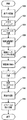
図4に、本発明の実施形態による発光素子の製造方法を示す。図4に見られるように、上記のような発光素子が製造される(ブロック200)。(例えば、分離トレンチ(例えば、分離トレンチ132)が形成されるように)この発光素子の各層がエッチングされ、メサを形成する(ブロック202)。活性層上のコンタクトがその後、得られたメサ上に形成される(ブロック203)。ウェーハが上述したように切断される領域において基板内に伸ばされるトレンチ(例えば、第2のトレンチ134)が形成され、およびメサの周囲に形成されることになる(ブロック204)。パッシベーション層がメサおよびトレンチの露出面上に形成される(ブロック206)。このパッシベーション層内に開口部が形成され、共晶金属コンタクトが形成される(ブロック207)。任意で、デバイスの活性領域の反対側のデバイスの基板は、(例えば、成形トレンチ136などの成形トレンチを形成することによって)成形される(ブロック208)。これらのデバイスはその後、素子を分割する線に沿ってウェーハを切断することにより(個々の素子またはいくつかの素子の組を形成するために)個片切断される(ブロック210)。 FIG. 4 shows a method for manufacturing a light emitting device according to an embodiment of the present invention. As seen in FIG. 4, the light emitting device as described above is manufactured (block 200). Each layer of the light emitting device is etched to form a mesa (eg, so that an isolation trench (eg, isolation trench 132) is formed) (block 202). A contact on the active layer is then formed on the resulting mesa (block 203). A trench (e.g., second trench 134) that extends into the substrate in the region where the wafer is cut as described above will be formed and formed around the mesa (block 204). A passivation layer is formed on the exposed surfaces of the mesas and trenches (block 206). Openings are formed in the passivation layer to form eutectic metal contacts (block 207). Optionally, the device substrate opposite the active region of the device is shaped (eg, by forming a shaped trench, such as shaped trench 136) (block 208). These devices are then cut into pieces (block 210) by cutting the wafer along lines that divide the elements (to form individual elements or sets of elements).
図5に、エピタキシャル層側のトレンチ製造中に保護層が設けられる本発明の実施形態による発光素子の製造方法を示す。図5に見られるように、上記のような発光素子が製造される(ブロック300)。(例えば、分離トレンチ(例えば、分離トレンチ132)が形成されるように)この発光素子の各層がエッチングされてメサを形成する(ブロック302)。活性層上のコンタクトがその後、得られたメサ上に形成される(ブロック304)。得られたメサ上にメサの側壁を含む犠牲保護層が形成される(ブロック306)。この保護層は、エピタキシャル層側のトレンチ形成中に活性領域を汚染または物理的損傷から保護するために設けてもよい。特定の実施形態では、この保護層は、例えば、窒化珪素、シリコン酸窒化物、二酸化珪素などの誘電層でもよく、あるいはフォトレジスト材料でもよい。しかし、トレンチ形成時にメサを保護できる材料であればどんなものでも用いることができる。 FIG. 5 shows a method for manufacturing a light emitting device according to an embodiment of the present invention in which a protective layer is provided during manufacturing of the trench on the epitaxial layer side. As seen in FIG. 5, the light emitting device as described above is manufactured (block 300). Each layer of the light emitting device is etched to form a mesa (eg, so that an isolation trench (eg, isolation trench 132) is formed) (block 302). Contacts on the active layer are then formed on the resulting mesa (block 304). A sacrificial protective layer including the mesa sidewalls is formed on the resulting mesa (block 306). This protective layer may be provided to protect the active region from contamination or physical damage during trench formation on the epitaxial layer side. In certain embodiments, the protective layer may be a dielectric layer such as, for example, silicon nitride, silicon oxynitride, silicon dioxide, or a photoresist material. However, any material that can protect the mesa during trench formation can be used.
基板内の領域に伸び、そこでウェーハが上述したように切断されるトレンチ(例えば、第2のトレンチ134)が形成され、かつメサの周囲に形成することができる(ブロック308)。特定の実施形態において、このトレンチは、切断加工切断に起因する汚染または物理的損傷からメサを保護するようにメサの側壁上に犠牲保護層の少なくとも一部を残したまま、例えば切断加工またはレーザースクライビングにより犠牲保護層まで形成される。トレンチ形成の完了後、この犠牲保護層はメサから取り除かれる(ブロック310)。犠牲保護層を除去する特定の方法は犠牲保護層の性質によって異なる。誘電層およびフォトレジスト層を除去する方法は当業者によく知られている。 A trench (eg, second trench 134) is formed that extends into a region in the substrate where the wafer is cut as described above and can be formed around the mesa (block 308). In certain embodiments, the trench may leave at least a portion of the sacrificial protective layer on the sidewalls of the mesa to protect the mesa from contamination or physical damage due to the cutting process, such as a cutting process or a laser. The sacrificial protective layer is formed by scribing. After completing the trench formation, the sacrificial protective layer is removed from the mesa (block 310). The particular method for removing the sacrificial protective layer depends on the nature of the sacrificial protective layer. Methods for removing the dielectric and photoresist layers are well known to those skilled in the art.
パッシベーション層がメサおよびトレンチの露出面上に形成される(ブロック312)。このパッシベーション層内に開口部が形成され、共晶金属コンタクトが形成される(ブロック314)。任意で、デバイスの活性領域の反対側のデバイスの基板を、(例えば、成形トレンチ136などの成形トレンチを形成することによって)成形することができる(ブロック316)。これらのデバイスはその後、素子を分割する線に沿ってウェーハを切断することにより(個々の素子かまたはいくつかの素子の組を形成するために)個片切断される(ブロック318)。 A passivation layer is formed on the exposed surfaces of the mesas and trenches (block 312). Openings are formed in the passivation layer to form eutectic metal contacts (block 314). Optionally, the device substrate opposite the active region of the device can be shaped (eg, by forming a shaped trench, such as shaped trench 136) (block 316). These devices are then cut into pieces (block 318) by cutting the wafer along lines dividing the elements (to form individual elements or sets of elements).
本発明の特定の実施形態において、基板の成形は切断加工操作または溝切り(scoring)操作により実現することができ、その操作では基板の切断加工または溝切りによって基板の成形部の範囲が定まる。例えば、ウェーハに線を刻むのに使用される切断加工用ブレードによってATON形(例えば、上部に立方体部分がある角錐台)を規定することができる。このような切断加工切断部はその後各デバイスを個片切断する切断線として使用することができる。 In a specific embodiment of the present invention, the forming of the substrate can be realized by a cutting process or a scoring operation, and the operation defines a range of a forming part of the substrate by the cutting process or the grooving of the substrate. For example, an ATON shape (eg, a truncated pyramid with a cubic portion on top) can be defined by a cutting blade used to engrave a line on a wafer. Such a cutting process cutting part can be used as a cutting line for cutting each device into individual pieces.
上記で説明したように、第2のトレンチ134はレーザスクライブで形成することができる。より詳細に説明すると、基板120部、および必要に応じて上に重なった任意の層(例えば、活性素子領域122が形成される層)をアブレーションにより除去するのにレーザを用いることができる。任意の適切なレーザを使用することができる。いくつかの実施形態によれば、Nd−YAG、エキシマまたはその他の短波長レーザが使用される。
As described above, the
さらに、デバイス製造の各操作が、特定の順序に関して図4および5に示されているが、本発明の実施形態は、このような順序に限定されると解釈されるべきではない。例えば、トレンチ(例えば、トレンチ134)は、メサを形成する前に形成してもよく、あるいはパッシベーション層形成後に形成してもよい。パッシベーション層形成後のトレンチ形成は、フリップチップ実装されないデバイスに適しているだろう。それゆえ、本発明は、図4および5に示された特定順序の操作に限定されると解釈されるべきではない。 In addition, although each device fabrication operation is illustrated in FIGS. 4 and 5 in a particular order, embodiments of the invention should not be construed as limited to such order. For example, the trench (eg, trench 134) may be formed before the mesa is formed, or may be formed after the passivation layer is formed. Trench formation after passivation layer formation may be suitable for devices that are not flip chip mounted. Therefore, the present invention should not be construed as limited to the particular order of operations shown in FIGS.
デバイス分離トレンチおよび第2のトレンチに関して本発明を説明してきたが、本開示に照らして当業者には了解されるように、単一のトレンチで分離トレンチと第2のトレンチの両方を形成してもよい。さらに、3つ以上のトレンチを設けることもできる。それゆえ、本発明の実施形態は、特定数の個別のトレンチに限定されると解釈されるべきではない。 Although the present invention has been described with respect to a device isolation trench and a second trench, as will be appreciated by those skilled in the art in light of this disclosure, a single trench may form both the isolation trench and the second trench. Also good. Further, more than two trenches can be provided. Therefore, embodiments of the present invention should not be construed as limited to a particular number of individual trenches.
窒化ガリウムから成る素子に関して本発明の実施形態を説明してきたが、本発明の教示と利益は、その他の第III族窒化物またはその他の半導体材料においても享受することができる。さらに、図3に示すように立方体部分および角錐台部分を有する成形基板に関して本発明の実施形態を説明してきたが、他の形の基板を利用することができる。それゆえ、本発明の実施形態は、本明細書で説明した特定の形に限定されると解釈されるべきではない。 Although embodiments of the present invention have been described with respect to devices made of gallium nitride, the teachings and benefits of the present invention can be enjoyed in other Group III nitrides or other semiconductor materials. Furthermore, while embodiments of the present invention have been described with respect to a molded substrate having a cubical portion and a truncated pyramid portion as shown in FIG. 3, other forms of substrates can be utilized. Therefore, embodiments of the present invention should not be construed as limited to the specific forms set forth herein.
LEDおよび/またはレーザに関して説明したが、本発明の方法と部材は、ダイオード、トランジスタ、サイリスタなどの個片切断されているその他のデバイスに使用することもできる。 Although described with respect to LEDs and / or lasers, the methods and components of the present invention may be used with other devices that are cut into pieces, such as diodes, transistors, thyristors, and the like.
以上のことは本発明を説明するものであって、本発明を限定するものと解釈されるべきではない。本発明の例示的な実施形態について説明してきたが、本発明の新規の教示と利点から著しく逸脱することなく例示的な実施形態において多くの変更された形態が可能であることを当業者は容易に理解するであろう。したがって、このような変更された形態は、すべて本発明の範囲内に含まれるものである。その結果、以上のことは本発明を説明するものであって、開示された特定の実施形態に限定されると解釈されべきではないこと、および開示された実施形態に対する変更された形態、ならびにその他の実施形態は本発明の範囲内に含まれるものである。 The foregoing is illustrative of the invention and should not be construed as limiting the invention. While exemplary embodiments of the present invention have been described, those skilled in the art will readily appreciate that many variations are possible in the exemplary embodiments without significantly departing from the novel teachings and advantages of the present invention. Will understand. Accordingly, all such modified forms are included within the scope of the present invention. As a result, the foregoing is illustrative of the invention and is not to be construed as limited to the particular embodiments disclosed, and variations to the disclosed embodiments and others These embodiments are included within the scope of the present invention.
Claims (19)
前記第1のデバイス部と第2のデバイス部との間の前記基板の前記第1の面に第1のトレンチを形成するステップと、
前記少なくとも1つのデバイス層内に、前記第1のデバイス部を含む第1のメサおよび前記第2のデバイス部を含む第2のメサの範囲を定める分離トレンチを形成するステップと、
前記基板の前記第2の面側の前記分離トレンチの中から前記基板へと伸びて前記第1のデバイス部と第2のデバイス部との間の前記基板の前記第2の面において第2のトレンチを形成するステップと、
前記第1のトレンチおよび前記第2のトレンチに沿って前記基板を切断して、前記基板の第1の部分および前記第1のデバイス部を含む第1のダイならびに前記基板の第2の部分および前記第2のデバイス部を含む第2のダイを形成するステップと、
を備え、前記第1のトレンチは少なくとも50μmの幅を有し、前記第2のトレンチは2〜25μmの幅を有する、
ことを特徴とする方法。Forming a semiconductor device using a semiconductor substrate having opposing first and second surfaces and at least one device layer on the second surface of the substrate including first and second device portions A way to
Forming a first trench in the first surface of the substrate between the first device portion and the second device portion;
Forming isolation trenches in the at least one device layer defining a first mesa including the first device portion and a second mesa including the second device portion;
The second surface of the substrate between the first device portion and the second device portion extends from the isolation trench on the second surface side of the substrate to the substrate and is second in the second surface of the substrate. Forming a trench;
Cutting the substrate along the first trench and the second trench, a first die including the first portion of the substrate and the first device portion, and a second portion of the substrate; Forming a second die including the second device portion;
Wherein the first trench has a width of at least 50 μm, and the second trench has a width of 2 to 25 μm.
A method characterized by that.
前記少なくとも1つのデバイス層内に、前記第1のデバイス部を含む第1のメサおよび前記第2のデバイス部を含む第2のメサの範囲を定める分離トレンチを形成するステップと、
前記第1および第2のメサ上に犠牲層を形成するステップと、
前記犠牲層が前記第1および第2のメサ上に配置されている間に、前記基板のデバイス面側の前記分離トレンチの中から前記基板へと伸びて前記第1のデバイス部と第2のデバイス部との間の前記基板のデバイス面において第2のトレンチを形成するステップと、
前記犠牲層を除去するステップと、
前記第2のトレンチに沿って前記基板を切断して、前記基板の第1の部分および前記第1のデバイス部を含む第1のダイならびに前記基板の第2の部分および前記第2のデバイス部を含む第2のダイを形成するステップと、を備えたことを特徴とする方法。A method of forming a semiconductor device using a semiconductor substrate having a device surface and at least one device layer on the device surface of the substrate including first and second device portions comprising:
Forming isolation trenches in the at least one device layer defining a first mesa including the first device portion and a second mesa including the second device portion;
Forming a sacrificial layer on the first and second mesas;
While the sacrificial layer is disposed on the first and second mesas, the first device portion and the second device extend from the isolation trench on the device surface side of the substrate to the substrate. Forming a second trench in the device surface of the substrate between the device portion;
Removing the sacrificial layer;
And cutting the substrate along the second trench, the second portion of the first die and the substrate including a first portion and the first device portion of the substrate and the second device part method characterized by comprising the steps of: forming a second die including.
前記第1のデバイス部と前記第2のデバイス部との間の前記基板の前記第1の面において立方体の頂点を備えた角錐台を定めるように第1のトレンチを形成するステップと、
前記少なくとも1つのデバイス層内に、前記第1のデバイス部を含む第1のメサおよび前記第2のデバイス部を含む第2のメサの範囲を定める分離トレンチを形成するステップと、
前記基板の第2の面側の前記分離トレンチの中から前記基板へと伸びて前記第1のデバイス部と第2のデバイス部との間の前記基板の前記第2の面において第2のトレンチを形成するステップと、
前記第1のトレンチおよび前記第2のトレンチに沿って前記基板を切断して、前記基板の第1の部分および前記第1のデバイス部を含む第1のダイならびに前記基板の第2の部分および前記第2のデバイス部を含む第2のダイを形成するステップと、を備えることを特徴とする方法。Forming a semiconductor device using a semiconductor substrate having opposing first and second surfaces and at least one device layer on the second surface of the substrate including first and second device portions A way to
Forming a first trench so as to define a truncated pyramid with a cubic vertex on the first surface of the substrate between the first device portion and the second device portion;
Forming isolation trenches in the at least one device layer defining a first mesa including the first device portion and a second mesa including the second device portion;
A second trench in the second surface of the substrate between the first device portion and the second device portion extending from the isolation trench on the second surface side of the substrate to the substrate; Forming a step ;
Cutting the substrate along the first trench and the second trench, a first die including the first portion of the substrate and the first device portion, and a second portion of the substrate; Forming a second die that includes the second device portion .
前記少なくとも1つのデバイス層内に、前記第1のデバイス部を含む第1のメサおよび前記第2のデバイス部を含む第2のメサの範囲を定める分離トレンチを形成するステップと、
前記基板のデバイス面側の前記分離トレンチの中から前記基板へと伸びて前記第1のデバイス部と第2のデバイス部との間の前記基板の前記デバイス面において第2のトレンチを形成するステップと、
前記第2のトレンチに沿って前記基板を切断して、前記基板の第1の部分および前記第1のデバイス部を含む第1のダイならびに前記基板の第2の部分および前記第2のデバイス部を含む第2のダイを形成するステップと、を備え、
前記第2のトレンチを形成するステップは、前記第2のトレンチを前記基板のデバイス面内にレーザースクライビングするステップで形成することを特徴とする方法。A method of forming a semiconductor device using a semiconductor substrate having a device surface and at least one device layer on the device surface of the substrate including first and second device portions comprising:
Forming isolation trenches in the at least one device layer defining a first mesa including the first device portion and a second mesa including the second device portion;
Extending from the isolation trench on the device surface side of the substrate to the substrate to form a second trench in the device surface of the substrate between the first device portion and the second device portion When,
Cutting the substrate along the second trench to form a first die including the first portion of the substrate and the first device portion; and a second portion of the substrate and the second device portion. Forming a second die comprising :
The method of forming the second trench comprises forming the second trench by laser scribing in the device surface of the substrate.
Applications Claiming Priority (7)
| Application Number | Priority Date | Filing Date | Title |
|---|---|---|---|
| US39748802P | 2002-07-19 | 2002-07-19 | |
| US60/397,488 | 2002-07-19 | ||
| US41589802P | 2002-10-03 | 2002-10-03 | |
| US60/415,898 | 2002-10-03 | ||
| US10/610,329 | 2003-06-30 | ||
| US10/610,329 US6995032B2 (en) | 2002-07-19 | 2003-06-30 | Trench cut light emitting diodes and methods of fabricating same |
| PCT/US2003/022411 WO2004010510A2 (en) | 2002-07-19 | 2003-07-11 | Trench cut light emitting diodes and methods of fabricating same |
Publications (3)
| Publication Number | Publication Date |
|---|---|
| JP2006510232A JP2006510232A (en) | 2006-03-23 |
| JP2006510232A5 JP2006510232A5 (en) | 2006-08-24 |
| JP4903434B2 true JP4903434B2 (en) | 2012-03-28 |
Family
ID=31999181
Family Applications (1)
| Application Number | Title | Priority Date | Filing Date |
|---|---|---|---|
| JP2005505523A Expired - Lifetime JP4903434B2 (en) | 2002-07-19 | 2003-07-11 | Trench cut type light emitting diode and method of manufacturing the same |
Country Status (9)
| Country | Link |
|---|---|
| US (2) | US6995032B2 (en) |
| EP (1) | EP1523768B1 (en) |
| JP (1) | JP4903434B2 (en) |
| KR (2) | KR20110017467A (en) |
| CN (1) | CN100375242C (en) |
| AU (1) | AU2003252005A1 (en) |
| MY (1) | MY138543A (en) |
| TW (1) | TWI283491B (en) |
| WO (1) | WO2004010510A2 (en) |
Families Citing this family (183)
| Publication number | Priority date | Publication date | Assignee | Title |
|---|---|---|---|---|
| JP3705791B2 (en) * | 2002-03-14 | 2005-10-12 | 株式会社東芝 | Semiconductor light emitting element and semiconductor light emitting device |
| CN1729582A (en) * | 2002-12-20 | 2006-02-01 | 克里公司 | Methods of forming electronic devices including semiconductor mesa structures and conductivity junctions and related devices |
| US6885033B2 (en) * | 2003-03-10 | 2005-04-26 | Cree, Inc. | Light emitting devices for light conversion and methods and semiconductor chips for fabricating the same |
| JP4342832B2 (en) * | 2003-05-16 | 2009-10-14 | 株式会社東芝 | Semiconductor device and manufacturing method thereof |
| CN100386890C (en) * | 2004-04-05 | 2008-05-07 | 清华大学 | Method of mfg. GaN-base LED |
| JP2008508561A (en) * | 2004-07-30 | 2008-03-21 | ノバラックス,インコーポレイティド | Apparatus, system, and method for wavelength conversion of mode-locked extended cavity surface emitting semiconductor laser |
| JP2006086516A (en) * | 2004-08-20 | 2006-03-30 | Showa Denko Kk | Method for manufacturing semiconductor light emitting device |
| US8174037B2 (en) * | 2004-09-22 | 2012-05-08 | Cree, Inc. | High efficiency group III nitride LED with lenticular surface |
| US7737459B2 (en) * | 2004-09-22 | 2010-06-15 | Cree, Inc. | High output group III nitride light emitting diodes |
| US7394158B2 (en) * | 2004-10-21 | 2008-07-01 | Siliconix Technology C.V. | Solderable top metal for SiC device |
| US7812441B2 (en) | 2004-10-21 | 2010-10-12 | Siliconix Technology C.V. | Schottky diode with improved surge capability |
| US9508886B2 (en) | 2007-10-06 | 2016-11-29 | Solexel, Inc. | Method for making a crystalline silicon solar cell substrate utilizing flat top laser beam |
| US8399331B2 (en) | 2007-10-06 | 2013-03-19 | Solexel | Laser processing for high-efficiency thin crystalline silicon solar cell fabrication |
| US8420435B2 (en) * | 2009-05-05 | 2013-04-16 | Solexel, Inc. | Ion implantation fabrication process for thin-film crystalline silicon solar cells |
| US9419092B2 (en) * | 2005-03-04 | 2016-08-16 | Vishay-Siliconix | Termination for SiC trench devices |
| US7834376B2 (en) | 2005-03-04 | 2010-11-16 | Siliconix Technology C. V. | Power semiconductor switch |
| US20060226442A1 (en) * | 2005-04-07 | 2006-10-12 | An-Ping Zhang | GaN-based high electron mobility transistor and method for making the same |
| JP4694263B2 (en) * | 2005-06-03 | 2011-06-08 | Okiセミコンダクタ株式会社 | Bonding substrate cutting method |
| JP2007158132A (en) * | 2005-12-06 | 2007-06-21 | Toyoda Gosei Co Ltd | Group iii nitride-based compound semiconductor element and manufacturing method thereof |
| JP5022576B2 (en) * | 2005-07-08 | 2012-09-12 | 株式会社ジャパンディスプレイイースト | Display panel and display device |
| US8368165B2 (en) | 2005-10-20 | 2013-02-05 | Siliconix Technology C. V. | Silicon carbide Schottky diode |
| TWM292164U (en) * | 2005-12-23 | 2006-06-11 | Inpaq Technology Co Ltd | Miniature electronic circuit protection element |
| KR20080106402A (en) * | 2006-01-05 | 2008-12-05 | 일루미텍스, 인크. | Separate optical device for directing light from an led |
| JP2007184426A (en) * | 2006-01-06 | 2007-07-19 | Shinko Electric Ind Co Ltd | Manufacturing method of semiconductor device |
| JP4707188B2 (en) * | 2006-03-17 | 2011-06-22 | 株式会社リコー | Image forming apparatus and toner |
| JP4945167B2 (en) * | 2006-05-12 | 2012-06-06 | スタンレー電気株式会社 | Manufacturing method of semiconductor light emitting device and mounting method of semiconductor light emitting device manufactured by the manufacturing method |
| JP2009538532A (en) | 2006-05-23 | 2009-11-05 | クリー エル イー ディー ライティング ソリューションズ インコーポレイテッド | Lighting device |
| KR101113878B1 (en) | 2006-06-23 | 2012-03-09 | 엘지이노텍 주식회사 | Light emitting diode having vertical topology and method of making the same |
| EP2047514A4 (en) | 2006-07-31 | 2010-12-01 | Vishay Siliconix | Molybdenum barrier metal for sic schottky diode and process of manufacture |
| DE102006043163B4 (en) * | 2006-09-14 | 2016-03-31 | Infineon Technologies Ag | Semiconductor circuitry |
| KR101262386B1 (en) | 2006-09-25 | 2013-05-08 | 엘지이노텍 주식회사 | Method for manufacturing nitride semiconductor light emitting device |
| US20090275266A1 (en) * | 2006-10-02 | 2009-11-05 | Illumitex, Inc. | Optical device polishing |
| WO2008042351A2 (en) | 2006-10-02 | 2008-04-10 | Illumitex, Inc. | Led system and method |
| US20080264477A1 (en) * | 2006-10-09 | 2008-10-30 | Soltaix, Inc. | Methods for manufacturing three-dimensional thin-film solar cells |
| US7999174B2 (en) * | 2006-10-09 | 2011-08-16 | Solexel, Inc. | Solar module structures and assembly methods for three-dimensional thin-film solar cells |
| US20100304521A1 (en) * | 2006-10-09 | 2010-12-02 | Solexel, Inc. | Shadow Mask Methods For Manufacturing Three-Dimensional Thin-Film Solar Cells |
| US8193076B2 (en) | 2006-10-09 | 2012-06-05 | Solexel, Inc. | Method for releasing a thin semiconductor substrate from a reusable template |
| US8035028B2 (en) * | 2006-10-09 | 2011-10-11 | Solexel, Inc. | Pyramidal three-dimensional thin-film solar cells |
| US8293558B2 (en) * | 2006-10-09 | 2012-10-23 | Solexel, Inc. | Method for releasing a thin-film substrate |
| US8084684B2 (en) | 2006-10-09 | 2011-12-27 | Solexel, Inc. | Three-dimensional thin-film solar cells |
| KR101381984B1 (en) | 2006-10-25 | 2014-04-10 | 서울바이오시스 주식회사 | Method for manufacturing light emitting diode chip and light emitting diode manufactured using the same |
| KR101252558B1 (en) * | 2006-11-06 | 2013-04-08 | 엘지이노텍 주식회사 | Method for making LED having vertical topology |
| US8143081B2 (en) * | 2007-02-13 | 2012-03-27 | Huga Optotech Inc. | Method for dicing a diced optoelectronic semiconductor wafer |
| US7833881B2 (en) * | 2007-03-02 | 2010-11-16 | Micron Technology, Inc. | Methods for fabricating semiconductor components and packaged semiconductor components |
| WO2009026240A1 (en) * | 2007-08-17 | 2009-02-26 | Solexel, Inc. | Methods for liquid transfer coating of three-dimensional substrates |
| US7985979B2 (en) * | 2007-12-19 | 2011-07-26 | Koninklijke Philips Electronics, N.V. | Semiconductor light emitting device with light extraction structures |
| US7622365B2 (en) * | 2008-02-04 | 2009-11-24 | Micron Technology, Inc. | Wafer processing including dicing |
| EP2240968A1 (en) * | 2008-02-08 | 2010-10-20 | Illumitex, Inc. | System and method for emitter layer shaping |
| US20100144080A1 (en) * | 2008-06-02 | 2010-06-10 | Solexel, Inc. | Method and apparatus to transfer coat uneven surface |
| US20110180781A1 (en) * | 2008-06-05 | 2011-07-28 | Soraa, Inc | Highly Polarized White Light Source By Combining Blue LED on Semipolar or Nonpolar GaN with Yellow LED on Semipolar or Nonpolar GaN |
| US20090309127A1 (en) * | 2008-06-13 | 2009-12-17 | Soraa, Inc. | Selective area epitaxy growth method and structure |
| US8847249B2 (en) * | 2008-06-16 | 2014-09-30 | Soraa, Inc. | Solid-state optical device having enhanced indium content in active regions |
| WO2009157921A1 (en) * | 2008-06-24 | 2009-12-30 | Pan Shaoher X | Silicon based solid state lighting |
| US20100006873A1 (en) * | 2008-06-25 | 2010-01-14 | Soraa, Inc. | HIGHLY POLARIZED WHITE LIGHT SOURCE BY COMBINING BLUE LED ON SEMIPOLAR OR NONPOLAR GaN WITH YELLOW LED ON SEMIPOLAR OR NONPOLAR GaN |
| US8805134B1 (en) | 2012-02-17 | 2014-08-12 | Soraa Laser Diode, Inc. | Methods and apparatus for photonic integration in non-polar and semi-polar oriented wave-guided optical devices |
| JP5282503B2 (en) * | 2008-09-19 | 2013-09-04 | 日亜化学工業株式会社 | Semiconductor light emitting device |
| EP2356675B1 (en) * | 2008-11-13 | 2016-06-01 | Solexel, Inc. | Three dimensional thin film solar cell and manufacturing method thereof |
| US8288195B2 (en) * | 2008-11-13 | 2012-10-16 | Solexel, Inc. | Method for fabricating a three-dimensional thin-film semiconductor substrate from a template |
| EP2371006A4 (en) * | 2008-11-26 | 2013-05-01 | Solexel Inc | Truncated pyramid structures for see-through solar cells |
| TW201034256A (en) * | 2008-12-11 | 2010-09-16 | Illumitex Inc | Systems and methods for packaging light-emitting diode devices |
| US8906218B2 (en) | 2010-05-05 | 2014-12-09 | Solexel, Inc. | Apparatus and methods for uniformly forming porous semiconductor on a substrate |
| WO2010083422A1 (en) * | 2009-01-15 | 2010-07-22 | Solexel, Inc. | Porous silicon electro-etching system and method |
| US9076642B2 (en) | 2009-01-15 | 2015-07-07 | Solexel, Inc. | High-Throughput batch porous silicon manufacturing equipment design and processing methods |
| US9343299B2 (en) | 2009-02-06 | 2016-05-17 | Solexel, Inc. | Trench formation method for releasing a substrate from a semiconductor template |
| MY162405A (en) * | 2009-02-06 | 2017-06-15 | Solexel Inc | Trench Formation Method For Releasing A Thin-Film Substrate From A Reusable Semiconductor Template |
| US8247886B1 (en) | 2009-03-09 | 2012-08-21 | Soraa, Inc. | Polarization direction of optical devices using selected spatial configurations |
| US8828517B2 (en) | 2009-03-23 | 2014-09-09 | Solexel, Inc. | Structure and method for improving solar cell efficiency and mechanical strength |
| US8252662B1 (en) * | 2009-03-28 | 2012-08-28 | Soraa, Inc. | Method and structure for manufacture of light emitting diode devices using bulk GaN |
| US8422525B1 (en) | 2009-03-28 | 2013-04-16 | Soraa, Inc. | Optical device structure using miscut GaN substrates for laser applications |
| US8299473B1 (en) | 2009-04-07 | 2012-10-30 | Soraa, Inc. | Polarized white light devices using non-polar or semipolar gallium containing materials and transparent phosphors |
| US8242522B1 (en) | 2009-05-12 | 2012-08-14 | Soraa, Inc. | Optical device structure using non-polar GaN substrates and growth structures for laser applications in 481 nm |
| US8294179B1 (en) | 2009-04-17 | 2012-10-23 | Soraa, Inc. | Optical device structure using GaN substrates and growth structures for laser applications |
| US8634442B1 (en) | 2009-04-13 | 2014-01-21 | Soraa Laser Diode, Inc. | Optical device structure using GaN substrates for laser applications |
| CN102396083B (en) | 2009-04-13 | 2015-12-16 | 天空激光二极管有限公司 | For the structure of optical means of the use GAN substrate of laser application |
| US8837545B2 (en) | 2009-04-13 | 2014-09-16 | Soraa Laser Diode, Inc. | Optical device structure using GaN substrates and growth structures for laser applications |
| US8254425B1 (en) | 2009-04-17 | 2012-08-28 | Soraa, Inc. | Optical device structure using GaN substrates and growth structures for laser applications |
| CN102427971B (en) * | 2009-04-14 | 2015-01-07 | 速力斯公司 | High efficiency epitaxial chemical vapor deposition (cvd) reactor |
| US8416825B1 (en) | 2009-04-17 | 2013-04-09 | Soraa, Inc. | Optical device structure using GaN substrates and growth structure for laser applications |
| US9099584B2 (en) * | 2009-04-24 | 2015-08-04 | Solexel, Inc. | Integrated three-dimensional and planar metallization structure for thin film solar cells |
| MY165969A (en) | 2009-05-05 | 2018-05-18 | Solexel Inc | High-productivity porous semiconductor manufacturing equipment |
| US9318644B2 (en) | 2009-05-05 | 2016-04-19 | Solexel, Inc. | Ion implantation and annealing for thin film crystalline solar cells |
| US8445314B2 (en) * | 2009-05-22 | 2013-05-21 | Solexel, Inc. | Method of creating reusable template for detachable thin film substrate |
| US8791499B1 (en) | 2009-05-27 | 2014-07-29 | Soraa, Inc. | GaN containing optical devices and method with ESD stability |
| US9829780B2 (en) | 2009-05-29 | 2017-11-28 | Soraa Laser Diode, Inc. | Laser light source for a vehicle |
| US8247887B1 (en) | 2009-05-29 | 2012-08-21 | Soraa, Inc. | Method and surface morphology of non-polar gallium nitride containing substrates |
| US10108079B2 (en) | 2009-05-29 | 2018-10-23 | Soraa Laser Diode, Inc. | Laser light source for a vehicle |
| US8551866B2 (en) * | 2009-05-29 | 2013-10-08 | Solexel, Inc. | Three-dimensional thin-film semiconductor substrate with through-holes and methods of manufacturing |
| US9250044B1 (en) | 2009-05-29 | 2016-02-02 | Soraa Laser Diode, Inc. | Gallium and nitrogen containing laser diode dazzling devices and methods of use |
| US8509275B1 (en) | 2009-05-29 | 2013-08-13 | Soraa, Inc. | Gallium nitride based laser dazzling device and method |
| US9800017B1 (en) | 2009-05-29 | 2017-10-24 | Soraa Laser Diode, Inc. | Laser device and method for a vehicle |
| US8427590B2 (en) | 2009-05-29 | 2013-04-23 | Soraa, Inc. | Laser based display method and system |
| US8585253B2 (en) | 2009-08-20 | 2013-11-19 | Illumitex, Inc. | System and method for color mixing lens array |
| US8449128B2 (en) * | 2009-08-20 | 2013-05-28 | Illumitex, Inc. | System and method for a lens and phosphor layer |
| US20110056429A1 (en) * | 2009-08-21 | 2011-03-10 | Soraa, Inc. | Rapid Growth Method and Structures for Gallium and Nitrogen Containing Ultra-Thin Epitaxial Structures for Devices |
| US9000466B1 (en) | 2010-08-23 | 2015-04-07 | Soraa, Inc. | Methods and devices for light extraction from a group III-nitride volumetric LED using surface and sidewall roughening |
| US8314429B1 (en) | 2009-09-14 | 2012-11-20 | Soraa, Inc. | Multi color active regions for white light emitting diode |
| US8355418B2 (en) | 2009-09-17 | 2013-01-15 | Soraa, Inc. | Growth structures and method for forming laser diodes on {20-21} or off cut gallium and nitrogen containing substrates |
| US8750342B1 (en) | 2011-09-09 | 2014-06-10 | Soraa Laser Diode, Inc. | Laser diodes with scribe structures |
| US9293644B2 (en) | 2009-09-18 | 2016-03-22 | Soraa, Inc. | Power light emitting diode and method with uniform current density operation |
| DE112010003700T5 (en) | 2009-09-18 | 2013-02-28 | Soraa, Inc. | POWER LIGHT DIODE AND METHOD WITH POWER DENSITY OPERATION |
| US9583678B2 (en) | 2009-09-18 | 2017-02-28 | Soraa, Inc. | High-performance LED fabrication |
| US8933644B2 (en) | 2009-09-18 | 2015-01-13 | Soraa, Inc. | LED lamps with improved quality of light |
| US20130167915A1 (en) | 2009-12-09 | 2013-07-04 | Solexel, Inc. | High-efficiency photovoltaic back-contact solar cell structures and manufacturing methods using three-dimensional semiconductor absorbers |
| US20110186874A1 (en) * | 2010-02-03 | 2011-08-04 | Soraa, Inc. | White Light Apparatus and Method |
| US8740413B1 (en) | 2010-02-03 | 2014-06-03 | Soraa, Inc. | System and method for providing color light sources in proximity to predetermined wavelength conversion structures |
| US8905588B2 (en) | 2010-02-03 | 2014-12-09 | Sorra, Inc. | System and method for providing color light sources in proximity to predetermined wavelength conversion structures |
| US20110182056A1 (en) * | 2010-06-23 | 2011-07-28 | Soraa, Inc. | Quantum Dot Wavelength Conversion for Optical Devices Using Nonpolar or Semipolar Gallium Containing Materials |
| US10147850B1 (en) | 2010-02-03 | 2018-12-04 | Soraa, Inc. | System and method for providing color light sources in proximity to predetermined wavelength conversion structures |
| CN102844883B (en) | 2010-02-12 | 2016-01-20 | 速力斯公司 | For the manufacture of the two-sided reusable template of the Semiconductor substrate of photocell and microelectronic component |
| US9927611B2 (en) | 2010-03-29 | 2018-03-27 | Soraa Laser Diode, Inc. | Wearable laser based display method and system |
| US8451876B1 (en) | 2010-05-17 | 2013-05-28 | Soraa, Inc. | Method and system for providing bidirectional light sources with broad spectrum |
| KR101028277B1 (en) | 2010-05-25 | 2011-04-11 | 엘지이노텍 주식회사 | Light emitting device, method for fabricating the light emitting device, light emitting device package and lighting unit |
| US8193546B2 (en) * | 2010-06-04 | 2012-06-05 | Pinecone Energies, Inc. | Light-emitting-diode array with polymer between light emitting devices |
| WO2011156657A2 (en) | 2010-06-09 | 2011-12-15 | Solexel, Inc. | High productivity thin film deposition method and system |
| US9450143B2 (en) | 2010-06-18 | 2016-09-20 | Soraa, Inc. | Gallium and nitrogen containing triangular or diamond-shaped configuration for optical devices |
| MY158500A (en) | 2010-08-05 | 2016-10-14 | Solexel Inc | Backplane reinforcement and interconnects for solar cells |
| CN102130144B (en) * | 2010-09-28 | 2013-02-13 | 映瑞光电科技(上海)有限公司 | White LED chip and forming method thereof |
| TWI478378B (en) * | 2010-10-25 | 2015-03-21 | Advanced Optoelectronic Tech | Led and method of manufacturing the same |
| CN102456778B (en) | 2010-10-26 | 2014-11-05 | 展晶科技(深圳)有限公司 | Manufacturing method for light-emitting diode chips |
| US8816319B1 (en) | 2010-11-05 | 2014-08-26 | Soraa Laser Diode, Inc. | Method of strain engineering and related optical device using a gallium and nitrogen containing active region |
| US8975615B2 (en) | 2010-11-09 | 2015-03-10 | Soraa Laser Diode, Inc. | Method of fabricating optical devices using laser treatment of contact regions of gallium and nitrogen containing material |
| US9048170B2 (en) | 2010-11-09 | 2015-06-02 | Soraa Laser Diode, Inc. | Method of fabricating optical devices using laser treatment |
| US8193015B2 (en) * | 2010-11-17 | 2012-06-05 | Pinecone Energies, Inc. | Method of forming a light-emitting-diode array with polymer between light emitting devices |
| US9595813B2 (en) | 2011-01-24 | 2017-03-14 | Soraa Laser Diode, Inc. | Laser package having multiple emitters configured on a substrate member |
| US9025635B2 (en) | 2011-01-24 | 2015-05-05 | Soraa Laser Diode, Inc. | Laser package having multiple emitters configured on a support member |
| US8786053B2 (en) | 2011-01-24 | 2014-07-22 | Soraa, Inc. | Gallium-nitride-on-handle substrate materials and devices and method of manufacture |
| US9318875B1 (en) | 2011-01-24 | 2016-04-19 | Soraa Laser Diode, Inc. | Color converting element for laser diode |
| US9093820B1 (en) | 2011-01-25 | 2015-07-28 | Soraa Laser Diode, Inc. | Method and structure for laser devices using optical blocking regions |
| US9508904B2 (en) * | 2011-01-31 | 2016-11-29 | Cree, Inc. | Structures and substrates for mounting optical elements and methods and devices for providing the same background |
| WO2012123840A1 (en) * | 2011-03-14 | 2012-09-20 | Koninklijke Philips Electronics N.V. | Led having vertical contacts redistributed for flip chip mounting |
| US9287684B2 (en) | 2011-04-04 | 2016-03-15 | Soraa Laser Diode, Inc. | Laser package having multiple emitters with color wheel |
| US9748414B2 (en) | 2011-05-20 | 2017-08-29 | Arthur R. Zingher | Self-activated front surface bias for a solar cell |
| US8952395B2 (en) | 2011-07-26 | 2015-02-10 | Micron Technology, Inc. | Wafer-level solid state transducer packaging transducers including separators and associated systems and methods |
| US8686431B2 (en) | 2011-08-22 | 2014-04-01 | Soraa, Inc. | Gallium and nitrogen containing trilateral configuration for optical devices |
| US8497146B2 (en) | 2011-08-25 | 2013-07-30 | Micron Technology, Inc. | Vertical solid-state transducers having backside terminals and associated systems and methods |
| JP5803457B2 (en) * | 2011-09-08 | 2015-11-04 | 三菱電機株式会社 | Method for manufacturing laser diode element |
| KR101887448B1 (en) * | 2011-10-13 | 2018-08-13 | 삼성전자주식회사 | cutting method of light emitting element package with ceramic substrate and cutting method of workpiece with multi-layer structure |
| CN102376824B (en) * | 2011-10-18 | 2013-05-29 | 中国科学院上海技术物理研究所 | Manufacture method of table surface type indium gallium arsenic detector |
| US8912025B2 (en) | 2011-11-23 | 2014-12-16 | Soraa, Inc. | Method for manufacture of bright GaN LEDs using a selective removal process |
| GB201121864D0 (en) * | 2011-12-20 | 2012-02-01 | Mled Ltd | Improving display contrast |
| WO2013134432A1 (en) | 2012-03-06 | 2013-09-12 | Soraa, Inc. | Light emitting diodes with low refractive index material layers to reduce light guiding effects |
| TW201407747A (en) * | 2012-08-03 | 2014-02-16 | Chi Mei Lighting Tech Corp | Light-emitting diode structure and method for manufacturing the same |
| US8971368B1 (en) | 2012-08-16 | 2015-03-03 | Soraa Laser Diode, Inc. | Laser devices having a gallium and nitrogen containing semipolar surface orientation |
| US9978904B2 (en) | 2012-10-16 | 2018-05-22 | Soraa, Inc. | Indium gallium nitride light emitting devices |
| US8802471B1 (en) | 2012-12-21 | 2014-08-12 | Soraa, Inc. | Contacts for an n-type gallium and nitrogen substrate for optical devices |
| US9166372B1 (en) | 2013-06-28 | 2015-10-20 | Soraa Laser Diode, Inc. | Gallium nitride containing laser device configured on a patterned substrate |
| US8994033B2 (en) | 2013-07-09 | 2015-03-31 | Soraa, Inc. | Contacts for an n-type gallium and nitrogen substrate for optical devices |
| DE102013107971A1 (en) * | 2013-07-25 | 2015-01-29 | Osram Opto Semiconductors Gmbh | Optoelectronic semiconductor chip, semiconductor component and method for producing optoelectronic semiconductor chips |
| US9362715B2 (en) | 2014-02-10 | 2016-06-07 | Soraa Laser Diode, Inc | Method for manufacturing gallium and nitrogen bearing laser devices with improved usage of substrate material |
| US9520695B2 (en) | 2013-10-18 | 2016-12-13 | Soraa Laser Diode, Inc. | Gallium and nitrogen containing laser device having confinement region |
| US9379525B2 (en) | 2014-02-10 | 2016-06-28 | Soraa Laser Diode, Inc. | Manufacturable laser diode |
| US9368939B2 (en) | 2013-10-18 | 2016-06-14 | Soraa Laser Diode, Inc. | Manufacturable laser diode formed on C-plane gallium and nitrogen material |
| US9419189B1 (en) | 2013-11-04 | 2016-08-16 | Soraa, Inc. | Small LED source with high brightness and high efficiency |
| US9397314B2 (en) * | 2013-12-23 | 2016-07-19 | Universal Display Corporation | Thin-form light-enhanced substrate for OLED luminaire |
| US9209596B1 (en) | 2014-02-07 | 2015-12-08 | Soraa Laser Diode, Inc. | Manufacturing a laser diode device from a plurality of gallium and nitrogen containing substrates |
| US9871350B2 (en) | 2014-02-10 | 2018-01-16 | Soraa Laser Diode, Inc. | Manufacturable RGB laser diode source |
| US9520697B2 (en) | 2014-02-10 | 2016-12-13 | Soraa Laser Diode, Inc. | Manufacturable multi-emitter laser diode |
| CN103887377B (en) * | 2014-03-12 | 2016-04-27 | 江苏新广联科技股份有限公司 | Reduce the device technology of GaN base vertical structure LED electric leakage |
| US9564736B1 (en) | 2014-06-26 | 2017-02-07 | Soraa Laser Diode, Inc. | Epitaxial growth of p-type cladding regions using nitrogen gas for a gallium and nitrogen containing laser diode |
| US9246311B1 (en) | 2014-11-06 | 2016-01-26 | Soraa Laser Diode, Inc. | Method of manufacture for an ultraviolet laser diode |
| US9653642B1 (en) | 2014-12-23 | 2017-05-16 | Soraa Laser Diode, Inc. | Manufacturable RGB display based on thin film gallium and nitrogen containing light emitting diodes |
| US9666677B1 (en) | 2014-12-23 | 2017-05-30 | Soraa Laser Diode, Inc. | Manufacturable thin film gallium and nitrogen containing devices |
| TW201631716A (en) * | 2015-02-16 | 2016-09-01 | Xintec Inc | A chip scale sensing chip package module and a manufacturing method thereof |
| US10186833B2 (en) * | 2015-02-18 | 2019-01-22 | Ii-Vi Incorporated | Densely-spaced laser diode configurations |
| US11437775B2 (en) | 2015-08-19 | 2022-09-06 | Kyocera Sld Laser, Inc. | Integrated light source using a laser diode |
| US10938182B2 (en) | 2015-08-19 | 2021-03-02 | Soraa Laser Diode, Inc. | Specialized integrated light source using a laser diode |
| US10879673B2 (en) | 2015-08-19 | 2020-12-29 | Soraa Laser Diode, Inc. | Integrated white light source using a laser diode and a phosphor in a surface mount device package |
| US11437774B2 (en) | 2015-08-19 | 2022-09-06 | Kyocera Sld Laser, Inc. | High-luminous flux laser-based white light source |
| US9787963B2 (en) | 2015-10-08 | 2017-10-10 | Soraa Laser Diode, Inc. | Laser lighting having selective resolution |
| TW201721906A (en) | 2015-12-14 | 2017-06-16 | 億光電子工業股份有限公司 | Light emitting diode package structure and manufacturing method thereof |
| CN105576092B (en) * | 2016-01-29 | 2019-02-05 | 华灿光电(苏州)有限公司 | A kind of preparation method of light emitting diode |
| TWI583086B (en) * | 2016-07-18 | 2017-05-11 | 華星光通科技股份有限公司 | Heat dissipation structure of optical transmitter, and optical transmitter comprising thereof |
| US10771155B2 (en) | 2017-09-28 | 2020-09-08 | Soraa Laser Diode, Inc. | Intelligent visible light with a gallium and nitrogen containing laser source |
| JP7094694B2 (en) * | 2017-12-01 | 2022-07-04 | キヤノン株式会社 | Light emitting element array and exposure head and image forming device using this |
| US10222474B1 (en) | 2017-12-13 | 2019-03-05 | Soraa Laser Diode, Inc. | Lidar systems including a gallium and nitrogen containing laser light source |
| CN108381042A (en) * | 2018-03-23 | 2018-08-10 | 伊欧激光科技(苏州)有限公司 | Chip processing system and wafer processing method |
| US10551728B1 (en) | 2018-04-10 | 2020-02-04 | Soraa Laser Diode, Inc. | Structured phosphors for dynamic lighting |
| CN108962997A (en) * | 2018-07-25 | 2018-12-07 | 阳林涛 | A kind of power device and preparation method thereof |
| US11239637B2 (en) | 2018-12-21 | 2022-02-01 | Kyocera Sld Laser, Inc. | Fiber delivered laser induced white light system |
| US11421843B2 (en) | 2018-12-21 | 2022-08-23 | Kyocera Sld Laser, Inc. | Fiber-delivered laser-induced dynamic light system |
| US11884202B2 (en) | 2019-01-18 | 2024-01-30 | Kyocera Sld Laser, Inc. | Laser-based fiber-coupled white light system |
| US11228158B2 (en) | 2019-05-14 | 2022-01-18 | Kyocera Sld Laser, Inc. | Manufacturable laser diodes on a large area gallium and nitrogen containing substrate |
| US10903623B2 (en) | 2019-05-14 | 2021-01-26 | Soraa Laser Diode, Inc. | Method and structure for manufacturable large area gallium and nitrogen containing substrate |
Family Cites Families (25)
| Publication number | Priority date | Publication date | Assignee | Title |
|---|---|---|---|---|
| JPH06103751B2 (en) * | 1988-05-18 | 1994-12-14 | 三洋電機株式会社 | Silicon carbide light emitting diode device and method for manufacturing silicon carbide single crystal |
| US4966862A (en) * | 1989-08-28 | 1990-10-30 | Cree Research, Inc. | Method of production of light emitting diodes |
| DE4305296C3 (en) * | 1993-02-20 | 1999-07-15 | Vishay Semiconductor Gmbh | Method of manufacturing a radiation emitting diode |
| US5418190A (en) * | 1993-12-30 | 1995-05-23 | At&T Corp. | Method of fabrication for electro-optical devices |
| US5631190A (en) * | 1994-10-07 | 1997-05-20 | Cree Research, Inc. | Method for producing high efficiency light-emitting diodes and resulting diode structures |
| KR970008386A (en) * | 1995-07-07 | 1997-02-24 | 하라 세이지 | A method of dividing a substrate and a dividing device |
| DE19536438A1 (en) * | 1995-09-29 | 1997-04-03 | Siemens Ag | Semiconductor device and manufacturing process |
| JPH09270528A (en) | 1996-03-29 | 1997-10-14 | Sanyo Electric Co Ltd | Light emitting diode element and manufacturing method thereof |
| JP3954686B2 (en) | 1997-03-24 | 2007-08-08 | 平田機工株式会社 | Substrate transport apparatus and substrate transport method |
| US5923946A (en) * | 1997-04-17 | 1999-07-13 | Cree Research, Inc. | Recovery of surface-ready silicon carbide substrates |
| US5972781A (en) * | 1997-09-30 | 1999-10-26 | Siemens Aktiengesellschaft | Method for producing semiconductor chips |
| JP3532100B2 (en) * | 1997-12-03 | 2004-05-31 | 日本碍子株式会社 | Laser cleaving method |
| JP2000091636A (en) * | 1998-09-07 | 2000-03-31 | Rohm Co Ltd | Manufacture of semiconductor light emitting element |
| US6413839B1 (en) * | 1998-10-23 | 2002-07-02 | Emcore Corporation | Semiconductor device separation using a patterned laser projection |
| US6201264B1 (en) * | 1999-01-14 | 2001-03-13 | Lumileds Lighting, U.S., Llc | Advanced semiconductor devices fabricated with passivated high aluminum content III-V materials |
| JP2000261042A (en) | 1999-03-05 | 2000-09-22 | Toshiba Corp | Semiconductor light emitting element and manufacture of the same |
| JP2001176823A (en) * | 1999-12-17 | 2001-06-29 | Sharp Corp | Method for manufacturing nitride semiconductor chip |
| DE10006738C2 (en) * | 2000-02-15 | 2002-01-17 | Osram Opto Semiconductors Gmbh | Light-emitting component with improved light decoupling and method for its production |
| US6261929B1 (en) | 2000-02-24 | 2001-07-17 | North Carolina State University | Methods of forming a plurality of semiconductor layers using spaced trench arrays |
| JP2001284293A (en) * | 2000-03-31 | 2001-10-12 | Toyoda Gosei Co Ltd | Chip division method for semiconductor wafer |
| DE10054966A1 (en) | 2000-11-06 | 2002-05-16 | Osram Opto Semiconductors Gmbh | Component for optoelectronics |
| US6518079B2 (en) * | 2000-12-20 | 2003-02-11 | Lumileds Lighting, U.S., Llc | Separation method for gallium nitride devices on lattice-mismatched substrates |
| US6740906B2 (en) | 2001-07-23 | 2004-05-25 | Cree, Inc. | Light emitting diodes including modifications for submount bonding |
| DE10148227B4 (en) | 2001-09-28 | 2015-03-05 | Osram Opto Semiconductors Gmbh | Radiation-emitting semiconductor chip, method for its production and radiation-emitting component |
| US6580054B1 (en) * | 2002-06-10 | 2003-06-17 | New Wave Research | Scribing sapphire substrates with a solid state UV laser |
-
2003
- 2003-06-30 US US10/610,329 patent/US6995032B2/en not_active Expired - Lifetime
- 2003-07-11 JP JP2005505523A patent/JP4903434B2/en not_active Expired - Lifetime
- 2003-07-11 CN CNB038208806A patent/CN100375242C/en not_active Expired - Lifetime
- 2003-07-11 KR KR1020117003263A patent/KR20110017467A/en not_active Application Discontinuation
- 2003-07-11 EP EP03765692.3A patent/EP1523768B1/en not_active Expired - Lifetime
- 2003-07-11 AU AU2003252005A patent/AU2003252005A1/en not_active Abandoned
- 2003-07-11 WO PCT/US2003/022411 patent/WO2004010510A2/en active Application Filing
- 2003-07-11 KR KR1020057000855A patent/KR101098743B1/en active IP Right Grant
- 2003-07-18 TW TW092119743A patent/TWI283491B/en not_active IP Right Cessation
- 2003-07-18 MY MYPI20032705A patent/MY138543A/en unknown
-
2005
- 2005-11-14 US US11/273,008 patent/US7368756B2/en not_active Expired - Lifetime
Also Published As
| Publication number | Publication date |
|---|---|
| US20060079082A1 (en) | 2006-04-13 |
| AU2003252005A1 (en) | 2004-02-09 |
| US20040051118A1 (en) | 2004-03-18 |
| WO2004010510A2 (en) | 2004-01-29 |
| WO2004010510A8 (en) | 2005-06-16 |
| AU2003252005A8 (en) | 2004-02-09 |
| EP1523768A2 (en) | 2005-04-20 |
| US6995032B2 (en) | 2006-02-07 |
| JP2006510232A (en) | 2006-03-23 |
| MY138543A (en) | 2009-06-30 |
| CN100375242C (en) | 2008-03-12 |
| KR20050119635A (en) | 2005-12-21 |
| EP1523768B1 (en) | 2017-04-12 |
| KR20110017467A (en) | 2011-02-21 |
| WO2004010510A3 (en) | 2004-08-19 |
| TWI283491B (en) | 2007-07-01 |
| TW200417054A (en) | 2004-09-01 |
| KR101098743B1 (en) | 2011-12-23 |
| US7368756B2 (en) | 2008-05-06 |
| CN1679144A (en) | 2005-10-05 |
Similar Documents
| Publication | Publication Date | Title |
|---|---|---|
| JP4903434B2 (en) | Trench cut type light emitting diode and method of manufacturing the same | |
| TWI447966B (en) | Semiconductor light emitting device and method of fabricating semiconductor light emitting device | |
| US7932111B2 (en) | Substrate removal process for high light extraction LEDs | |
| US7858414B2 (en) | Nitride semiconductor device and manufacturing method thereof | |
| EP1730790B1 (en) | Fabrication of semiconductor devices | |
| US20080113460A1 (en) | Laser Lift-Off of Sapphire From a Nitride Flip-Chip | |
| EP2816617B1 (en) | Semiconductor optical emitting device with metallized sidewalls | |
| EP1956663A1 (en) | Nitride semiconductor light emitting element and method for producing nitride semiconductor light emitting element | |
| US20100314633A1 (en) | Front end scribing of light emitting diode (led) wafers and resulting devices | |
| KR20070042214A (en) | Nitride-based light emitting diode and manufacturing of the same | |
| JP2005505140A (en) | Beam emitting semiconductor chip, method of manufacturing the semiconductor chip, and beam emitting constituent element | |
| JP2011171327A (en) | Light emitting element, method for manufacturing the same, and light emitting device | |
| JP6568062B2 (en) | Dicing wafer of light emitting device | |
| KR100482174B1 (en) | Fabrication Method of GaN related LED using Substrate Remove Technology | |
| CN111029449B (en) | Deep ultraviolet thin film semiconductor device structure and manufacturing method thereof | |
| KR100629929B1 (en) | Light emitting diode having vertical electrode structure | |
| KR20050013042A (en) | Light emitting diode having vertical electrode structure, manufacturing method of the same and etching method of sapphire substrate | |
| KR20060134490A (en) | Flip-chip gan-based light emitting diode and manufacturing method of the same | |
| CA2493853A1 (en) | Trench cut light emitting diodes and methods of fabricating same | |
| JP2011160010A (en) | Method for manufacturing nitride semiconductor element | |
| KR20050055636A (en) | Light emitting diode having vertical electrode structure, manufacturing method of the same and etching method of sapphire substrate |
Legal Events
| Date | Code | Title | Description |
|---|---|---|---|
| A521 | Request for written amendment filed |
Free format text: JAPANESE INTERMEDIATE CODE: A523 Effective date: 20060705 |
|
| A621 | Written request for application examination |
Free format text: JAPANESE INTERMEDIATE CODE: A621 Effective date: 20060705 |
|
| A131 | Notification of reasons for refusal |
Free format text: JAPANESE INTERMEDIATE CODE: A131 Effective date: 20090807 |
|
| A521 | Request for written amendment filed |
Free format text: JAPANESE INTERMEDIATE CODE: A523 Effective date: 20091109 |
|
| A02 | Decision of refusal |
Free format text: JAPANESE INTERMEDIATE CODE: A02 Effective date: 20100817 |
|
| A521 | Request for written amendment filed |
Free format text: JAPANESE INTERMEDIATE CODE: A523 Effective date: 20101217 |
|
| RD02 | Notification of acceptance of power of attorney |
Free format text: JAPANESE INTERMEDIATE CODE: A7422 Effective date: 20101207 |
|
| A911 | Transfer to examiner for re-examination before appeal (zenchi) |
Free format text: JAPANESE INTERMEDIATE CODE: A911 Effective date: 20110225 |
|
| A912 | Re-examination (zenchi) completed and case transferred to appeal board |
Free format text: JAPANESE INTERMEDIATE CODE: A912 Effective date: 20110401 |
|
| A01 | Written decision to grant a patent or to grant a registration (utility model) |
Free format text: JAPANESE INTERMEDIATE CODE: A01 |
|
| A61 | First payment of annual fees (during grant procedure) |
Free format text: JAPANESE INTERMEDIATE CODE: A61 Effective date: 20120105 |
|
| R150 | Certificate of patent or registration of utility model |
Ref document number: 4903434 Country of ref document: JP Free format text: JAPANESE INTERMEDIATE CODE: R150 Free format text: JAPANESE INTERMEDIATE CODE: R150 |
|
| FPAY | Renewal fee payment (event date is renewal date of database) |
Free format text: PAYMENT UNTIL: 20150113 Year of fee payment: 3 |
|
| R250 | Receipt of annual fees |
Free format text: JAPANESE INTERMEDIATE CODE: R250 |
|
| R250 | Receipt of annual fees |
Free format text: JAPANESE INTERMEDIATE CODE: R250 |
|
| R250 | Receipt of annual fees |
Free format text: JAPANESE INTERMEDIATE CODE: R250 |
|
| R250 | Receipt of annual fees |
Free format text: JAPANESE INTERMEDIATE CODE: R250 |
|
| R250 | Receipt of annual fees |
Free format text: JAPANESE INTERMEDIATE CODE: R250 |
|
| R250 | Receipt of annual fees |
Free format text: JAPANESE INTERMEDIATE CODE: R250 |
|
| R250 | Receipt of annual fees |
Free format text: JAPANESE INTERMEDIATE CODE: R250 |
|
| R250 | Receipt of annual fees |
Free format text: JAPANESE INTERMEDIATE CODE: R250 |
|
| R250 | Receipt of annual fees |
Free format text: JAPANESE INTERMEDIATE CODE: R250 |
|
| EXPY | Cancellation because of completion of term |