EP1523768B1 - Method of forming semiconductor devices - Google Patents
Method of forming semiconductor devices Download PDFInfo
- Publication number
- EP1523768B1 EP1523768B1 EP03765692.3A EP03765692A EP1523768B1 EP 1523768 B1 EP1523768 B1 EP 1523768B1 EP 03765692 A EP03765692 A EP 03765692A EP 1523768 B1 EP1523768 B1 EP 1523768B1
- Authority
- EP
- European Patent Office
- Prior art keywords
- trench
- substrate
- forming
- depth
- layer
- Prior art date
- Legal status (The legal status is an assumption and is not a legal conclusion. Google has not performed a legal analysis and makes no representation as to the accuracy of the status listed.)
- Expired - Lifetime
Links
Images
Classifications
-
- H—ELECTRICITY
- H10—SEMICONDUCTOR DEVICES; ELECTRIC SOLID-STATE DEVICES NOT OTHERWISE PROVIDED FOR
- H10H—INORGANIC LIGHT-EMITTING SEMICONDUCTOR DEVICES HAVING POTENTIAL BARRIERS
- H10H20/00—Individual inorganic light-emitting semiconductor devices having potential barriers, e.g. light-emitting diodes [LED]
- H10H20/80—Constructional details
- H10H20/81—Bodies
- H10H20/819—Bodies characterised by their shape, e.g. curved or truncated substrates
-
- H—ELECTRICITY
- H10—SEMICONDUCTOR DEVICES; ELECTRIC SOLID-STATE DEVICES NOT OTHERWISE PROVIDED FOR
- H10H—INORGANIC LIGHT-EMITTING SEMICONDUCTOR DEVICES HAVING POTENTIAL BARRIERS
- H10H20/00—Individual inorganic light-emitting semiconductor devices having potential barriers, e.g. light-emitting diodes [LED]
- H10H20/80—Constructional details
- H10H20/81—Bodies
-
- H—ELECTRICITY
- H10—SEMICONDUCTOR DEVICES; ELECTRIC SOLID-STATE DEVICES NOT OTHERWISE PROVIDED FOR
- H10H—INORGANIC LIGHT-EMITTING SEMICONDUCTOR DEVICES HAVING POTENTIAL BARRIERS
- H10H20/00—Individual inorganic light-emitting semiconductor devices having potential barriers, e.g. light-emitting diodes [LED]
- H10H20/01—Manufacture or treatment
-
- H—ELECTRICITY
- H10—SEMICONDUCTOR DEVICES; ELECTRIC SOLID-STATE DEVICES NOT OTHERWISE PROVIDED FOR
- H10W—GENERIC PACKAGES, INTERCONNECTIONS, CONNECTORS OR OTHER CONSTRUCTIONAL DETAILS OF DEVICES COVERED BY CLASS H10
- H10W72/00—Interconnections or connectors in packages
- H10W72/50—Bond wires
- H10W72/531—Shapes of wire connectors
- H10W72/536—Shapes of wire connectors the connected ends being ball-shaped
-
- H—ELECTRICITY
- H10—SEMICONDUCTOR DEVICES; ELECTRIC SOLID-STATE DEVICES NOT OTHERWISE PROVIDED FOR
- H10W—GENERIC PACKAGES, INTERCONNECTIONS, CONNECTORS OR OTHER CONSTRUCTIONAL DETAILS OF DEVICES COVERED BY CLASS H10
- H10W72/00—Interconnections or connectors in packages
- H10W72/851—Dispositions of multiple connectors or interconnections
- H10W72/874—On different surfaces
- H10W72/884—Die-attach connectors and bond wires
Definitions
- This invention relates to fabrication methods for semiconductor devices, such as light emitting diodes (LEDs).
- LEDs light emitting diodes
- a light emitting diode generally includes a diode region on a microelectronic substrate.
- the microelectronic substrate may comprise, for example, gallium arsenide, gallium phosphide, alloys thereof, silicon carbide and/or sapphire.
- GaN-based light emitting diodes typically comprise an insulating, semiconducting or conducting substrate such as sapphire or SiC on which a plurality of GaN-based epitaxial layers are deposited.
- the epitaxial layers comprise an active region having a p-n junction that emits light when energized.
- a typical LED is mounted substrate side down onto a submount, also called a package or lead frame (hereinafter referred to as a "submount").
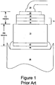
- Figure 1 schematically illustrates a conventional LED having an n-type SiC substrate 10, an active region 12 comprising an n-GaN-based layer 14 and a p-GaN-based layer 16 grown on the substrate and patterned into a mesa.
- a metal p-electrode 18 is deposited on and electrically coupled to the p-GaN layer 16 and a wire bond connection 28 is made to a bond pad 20 on the p-electrode 18.
- An n-electrode 22 that is on and electrically coupled to the conductive substrate is attached to metallic submount 24 using a conductive epoxy 26.
- the conductive epoxy 26 usually silver epoxy
- the LED is pressed into the epoxy 26.
- the epoxy is then heat cured which causes it to harden, providing a stable and electrically conductive mount for the LED chip.
- Light generated in the active region 12 is directed up and out of the device. However, a substantial amount of the generated light may be transmitted into the substrate and partially absorbed by the epoxy 26.
- Flip-chip mounting of LEDs involves mounting the LED onto the submount substrate side up. Light is then extracted and emitted through the transparent substrate.
- Flip chip mounting may be an especially desirable technique for mounting SiC-based LEDs. Because SiC has a higher index of refraction than GaN, light generated in the active region does not internally reflect ( i.e. reflect back into the GaN-based layers) at the GaN/SiC interface.
- Flip chip mounting of SiC-based LEDs may offer improved light extraction when employing certain chip-shaping techniques known in the art.
- Flip chip packaging of SiC LEDs may have other benefits as well, such as improved heat extraction/dissipation, which may be desirable depending on the particular application for the chip.
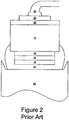
- FIG. 2 One problem with flip-chip mounting is illustrated in Figure 2 . Namely, when a chip is flip-chip mounted on a conductive submount or package conventional techniques may not be possible. Conventionally, a conductive die attach material 26, such as silver epoxy, is deposited on the chip and/or on the submount 24, and the chip is pressed onto the submount 24. This can cause the viscous conductive die attach material 26 to squeeze out and make contact with the n-type layers 14 and 10 in the device, thereby forming a Schottky diode connection that shunts the p-n junction in the active region with predictably undesirable results.
- a conductive die attach material 26 such as silver epoxy
- a further problem may arise from the stress applied to the side of the die during breaking when LED dies are singulated from a wafer by a sawing and breaking. This stress can cause fractures in the edge of the chip. If the fractures are bad enough, the die may be ruined. For example, if the fractures extend into the active regions of the device the device may be ruined.
- US6197609 discloses a method for forming semiconductor devices using a semiconductor substrate having first and second opposed sides, and at least one device layer on the second side of the substrate, the at least one device layer including first and second device portions, the method comprising the steps of: forming a first trench in the first side of the substrate between the first and second device portions; forming an isolation trench in the at least one device layer, the isolation trench defining a first mesa including the first device portion and a second mesa including the second device portion; forming a second trench in the second side of the substrate in and along the isolation trench between the first and second device portions; forming a SiOx protection layer over the first and second mesas and in the second trench; and breaking the substrate along the first and second trenches to form first and second dies, the first die including a first portion of the substrate and the first device portion, and the second die including a second portion of the substrate and the second device portion.
- US5429954 discloses a method for forming semiconductor devices using a semiconductor substrate having first and second opposed sides, and at least one device layer on the second side of the substrate, the at least one device layer including first and second device portions, the method comprising the steps of: forming an isolation trench in the at least one device layer, the isolation trench defining a first mesa including the first device portion and a second mesa including the second device portion; thereafter forming a SiOx sacrificial layer over the first and second mesas; thereafter forming a second trench in the second side of the substrate in the isolation trench between the first and second device portions to form first and second dies, whilst the sacrificial layer is disposed on the at least one device layer, the first die including a first portion of the substrate and the first device portion, and the second die including a second portion of the substrate and the second device portion; thereafter roughening (by wet-chemical etching) the lateral faces of the semiconductor substrate which are exposed after formation of the second trench; and thereafter removing the
- the present invention provides a method for forming semiconductor devices according to claim 1.
- the present invention provides a method for forming a semiconductor device such as, for example, a light emitting diode having a shaped substrate and that is suitable for flip-chip mounting.
- the light emitting diode has a trench that extends into the substrate of the device from the surface on which the active regions of the device ( e . g . an "epi" side of the device) are formed and opposite a shaped substrate side of the device.
- the epi-side trench may provide a stress relief or step to facilitate breaking of the wafer which may reduce yield loss due to propagation of breaks that extend into the junction of the device.
- the epi-side trench may enable the insulating passivation material to be deposited onto the post-trench cut wafer, effectively wrapping the passivation material around the trench cut.
- an insulating barrier may be provided against die attach materials (e . g . solder) making contact with the SiC substrate, thus creating a short or shunt between the p and n junctions of the device during die attach.
- the light emitting diode has a shaped substrate. Because of the high index of refraction of SiC, light passing through a SiC substrate tends to be totally internally reflected into the substrate at the surface of the substrate unless the light strikes the interface at a fairly low angle of incidence (i . e . fairly close to normal). The critical angle for total internal reflection depends on the material with which forms the interface with the SiC substrate. It is possible to increase the light output from a SiC-based LED by shaping the SiC substrate in a manner that limits total internal reflection by causing more rays to strike the surface of the SiC at low angles of incidence.
- One such chip shaping technique and resulting chip is shown in United States Patent Application Serial No. 10/057,821, filed January 25, 2002 , entitled "LIGHT EMITTING DIODES INCLUDING SUBSTRATE MODIFICATIONS FOR LIGHT EXTRACTION AND MANUFACTURING METHODS THEREFOR".
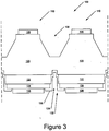
- Figure 3 illustrates LED chips having shaped substrates such as those described in the above referenced patent application prior to singulation.
- a wafer 100 includes LED chips 110 as shown in Figure 3 that include a substrate 120, such as a SiC substrate.
- An active device region 122 of the LED chips 110 may include Group III nitrides, such as GaN based layers.
- Contacts 124 and 128 are provided on the active device regions 122 and the substrate 120. Additionally, eutectic metal regions 126 may also be provided.
- the active regions 122 are formed into mesas by an isolation trench 132.
- the isolation trench 132 serves to define individual or groups of devices and is substantially aligned with the shaping trench (or cut) or "streets" 136 of the substrate 120 utilized to separate the devices and to provide the desired shape of the substrate.
- a second trench 134 is also formed in the substrate 120.
- the second trench 134 is also substantially aligned with the streets 136 of the substrate 120 and is formed within the isolation trench 132 that forms the mesa termination of the active regions 122.
- the second trench 134 is provided in a separate fabrication step after the formation of the isolation trench 132.
- the second trench 134 may be diced, sawn, etched, water sawn, laser scribed or created using other methods of standard hard material semiconductor separation or singulation techniques.
- the second trench 134 extends into the substrate 120 a distance sufficient to provide stress relief and/or facilitate the breaking of the substrate in the singulation process so as to reduce the propagation of the breaks into the active regions 122.
- the second trench 134 extends at least about 2 ⁇ m into the substrate 120.
- the second trench 134 extends at least about 5 ⁇ m into the substrate 120.
- the second trench 134 extends at least about 10 ⁇ m into the substrate 120.
- the second trench 134 extends at least about 20 ⁇ m into the substrate 120.
- the second trench 134 extends into the substrate 120 a depth of between about 2 and 5 ⁇ m. According to some embodiments, the depth of the second trench 134 into the substrate 120 is at least 1% of the thickness of the substrate 120. According to some preferred embodiments, a depth of the second trench 134 into the substrate 120 is between about 5 and 20% of the substrate 120.
- the second trench 134 may also have a width sufficient to provide stress relief and/or facilitate the breaking of the substrate in the singulation process so as to reduce the propagation of the breaks into the active regions 122.
- light emitting device structures may be provided as the active regions 122.
- the second trench 134 has a width of at least about 2 ⁇ m. In other embodiments, the second trench 134 has a width of at least about 5 ⁇ m. In other embodiments of the present invention, the second trench 134 has a width of at least about 10 ⁇ m. In a particular embodiment of the present invention, the second trench 134 has a width of at least about 25 ⁇ m. According to some embodiments, the second trench 134 has a width of between about 2 and 25 ⁇ m.
- the isolation trench 132 has a depth of at least about 1 ⁇ m. According to some preferred embodiments, the isolation trench 132 has a depth of between about 2 and 4 ⁇ m.
- the isolation trench 132 has a width of at least 30 ⁇ m. According to some preferred embodiments, the isolation trench 132 has a width of between about 50 and 70 ⁇ m.
- the shaping trench 136 has a depth into the substrate 120 of at least 100 ⁇ m. According to some preferred embodiments, the shaping trench 136 has a depth into the substrate of between about 200 and 220 ⁇ m.
- the shaping trench 136 has a width of at least 50 ⁇ m. According to some preferred embodiments, the shaping trench 136 has a width of between about 75 and 125 ⁇ m.
- the second trench 134 has a depth into the substrate 120 of between about 2 and 5 ⁇ m with the shaping trench 136 having a depth into the substrate 120 of between about 150 and 200 ⁇ m. According to some embodiments, the depth of the second trench 134 into the substrate 120 is between about 5 and 10% of the depth of the shaping trench 136 into the substrate. According to some embodiments, the thickness of the substrate 120 remaining between the second trench 134 and the shaping trench 136 is at least 5% of the original thickness of the substrate 120. According to some embodiments, the thickness of the substrate 120 remaining between the second trench 134 and the shaping trench 136 is between about 5 and 15% of the original thickness of the substrate 120.
- a passivation layer 130 such as an oxide, nitride and/or oxynitride, may be provided on the surfaces exposed by the isolation trench 132 and the second trench 134.
- the passivation layer 130 may extend into the substrate 120 a distance corresponding to the depth of the second trench 134.
- the passivation material can be Silicon Nitride (SiN), doped or undoped Silicon Dioxide (SiO 2 ), Silicon Oxy-Nitride (SiO x N y ), Spin-on Glass, Polyimide, or any other insulating material or combination of films, and may be deposited by CVD, LPCVD, PECVD, sputtering, or spin-on dispense of uncured liquid followed by a curing process.
- Formation of the passivation layer 130 into the substrate may provide protection against LED assembly shorts or shunts due to die attach material wicking around a p-n junction in the active regions 122.
- the depth of the second trench 134 may also be selected so as to reduce the likelihood of the formation of a parasitic Schottky diode when the device 110 is mounted.
- the active regions 122 may be gallium nitride based LEDs or lasers fabricated on a silicon carbide substrate such as those devices manufactured and sold by Cree, Inc. of Durham, North Carolina.
- the present invention may be suitable for use with LEDs and/or lasers as described in United States Patent Nos.
- the light emitting devices may include a p-electrode that provides a reflecting layer to reflect light generated in the active region back through the device.
- Reflective p-electrodes and related structures are described in U.S. Patent Application Serial No. 10/057,82 , entitled "LIGHT EMITTING DIODES INCLUDING SUBSTRATE MODIFICATIONS FOR LIGHT EXTRACTION AND MANUFACTURING METHODS THEREFOR", filed January 25, 2002.
- the LEDs and/or lasers may be configured to operate in a "flip-chip" configuration such that light emission occurs through the substrate.
- the substrate may be patterned so as to enhance light output of the devices as is described, for example, in United States Provisional Patent Application Ser. No. 60/307,235, filed July 23, 2001 , entitled “LIGHT EMITTING DIODES INCLUDING SUBSTRATE MODIFICATIONS FOR LIGHT EXTRACTION AND MANUFACTURING METHODS THEREFOR” and United States patent Application Serial No. 10/057,82, filed January 25, 2002 , entitled “LIGHT EMITTING DIODES INCLUDING SUBSTRATE MODIFICATIONS FOR LIGHT EXTRACTION AND MANUFACTURING METHODS THEREFOR.”
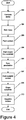
- Figure 4 illustrates methods of fabricating light emitting diodes not forming part of the present invention.
- a light emitting diode such as those described above is fabricated (block 200 ).
- the layers of the light emitting diode are etched ( e.g. , such that an isolation trench ( e . g., the isolation trench 132 ) is formed) to form a mesa (block 202 ).
- the contact on the active layers is then formed on the resulting mesa (block 203 ).
- a trench e . g. , the second trench 134
- a passivation layer is formed on the exposed surfaces of the mesa and the trench (block 206 ).
- An opening is formed in the passivation layer and the eutectic metal contact formed (block 207 ).
- the substrate of the device opposite the active regions of the device is shaped ( e . g ., by forming a shaping trench such as the shaping trench 136 ) (block 208 ).
- the devices are then singulated (either to form individual dies or groups of dies) by breaking the wafer along lines which divide the dies (block 210 ).
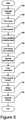
- Figure 5 illustrates methods of fabricating light emitting diodes according to embodiments of the present invention where a protective layer is provided during fabrication of the epi-side trench.
- a light emitting diode such as those described above is fabricated (block 300 ).
- the layers of the light emitting diode are etched such that an isolation trench (132) is formed to form a mesa (block 302 ).
- the contact on the active layers is then formed on the resulting mesa (block 304 ).
- a sacrificial protective layer is formed on the resulting mesa, including the sidewalls of the mesa (block 306 ).
- the protective layer is provided to protect the active region from contamination or physical damage during the formation of the epi-side trench.
- the protective layer may, for example, be a dielectric layer such as silicon nitride, silicon oxynitride, silicon dioxide or the like, or may be photoresist material. However, any material that may protect the mesa during formation of the trench may be utilized.
- a second trench (134) is formed that extends into the substrate in regions where the wafer is to be broken as described above and may be formed at the periphery of the mesa (block 308 ).
- the trench is formed by sawing or laser scribing, for example, through the sacrificial protective layer while at least a portion of the sacrificial protective layer remains on the sidewall of the mesa so as to protect the mesa from contaminants or physical damage resulting from the saw cut.
- the sacrificial protective layer is removed from the mesa (block 310 ).
- the particular technique for removal of the sacrificial protective layer will depend on the nature of the sacrificial protective layer. Methods for removing dielectric and photoresist layers are well known to those skilled in the art.
- a passivation layer is formed on the exposed surfaces of the mesa and the trench (block 312 ).
- An opening is formed in the passivation layer and the eutectic metal contact formed (block 314 ).
- the substrate of the device opposite the active regions of the device is shaped by forming a shaping trench such as the shaping trench 136 (block 316 ).
- the devices are then singulated (either to form individual dies or groups of dies) by breaking the wafer along lines which divide the dies (block 318 ).
- the shaping of the substrate may be provided by a sawing or scoring operation where the sawing or scoring of the substrate defines the shaped portion of the substrate.
- a saw blade used to cut lines in a wafer may define an ATON shape (e.g. a truncated pyramid with a cubic portion on top). Such saw cuts may then be used as break lines to singulate the devices.
- the second trench 134 may be formed by laser scribing. More particularly, a laser may be employed to remove portions of the substrate 120 and, as needed, any overlying layers (e . g ., the layers from which the active device regions 122 are formed) by ablation. Any suitable laser may be used. According to some embodiments, a Nd-YAG, excimer or other short wavelength laser is used.
- the methods and assemblies of the present invention may also be used for other devices that are singulated, such as diodes, transistors, thyristors or the like.
Landscapes
- Led Devices (AREA)
- Semiconductor Lasers (AREA)
- Led Device Packages (AREA)
Description
- This invention relates to fabrication methods for semiconductor devices, such as light emitting diodes (LEDs).
- Light emitting diodes are widely used in consumer and commercial applications. As is well known to those having skill in the art, a light emitting diode generally includes a diode region on a microelectronic substrate. The microelectronic substrate may comprise, for example, gallium arsenide, gallium phosphide, alloys thereof, silicon carbide and/or sapphire. Continued developments in LEDs have resulted in highly efficient and mechanically robust light sources that can cover the visible spectrum and beyond. These attributes, coupled with the potentially long service life of solid state devices, may enable a variety of new display applications, and may place LEDs in a position to compete with the well entrenched incandescent lamp.
- GaN-based light emitting diodes (LEDs) typically comprise an insulating, semiconducting or conducting substrate such as sapphire or SiC on which a plurality of GaN-based epitaxial layers are deposited. The epitaxial layers comprise an active region having a p-n junction that emits light when energized. A typical LED is mounted substrate side down onto a submount, also called a package or lead frame (hereinafter referred to as a "submount").
Figure 1 schematically illustrates a conventional LED having an n-type SiC substrate 10, an active region 12 comprising an n-GaN-basedlayer 14 and a p-GaN-basedlayer 16 grown on the substrate and patterned into a mesa. A metal p-electrode 18 is deposited on and electrically coupled to the p-GaN layer 16 and awire bond connection 28 is made to abond pad 20 on the p-electrode 18. An n-electrode 22 that is on and electrically coupled to the conductive substrate is attached tometallic submount 24 using aconductive epoxy 26. In the conventional process, the conductive epoxy 26 (usually silver epoxy) is deposited on the submount and the LED is pressed into theepoxy 26. The epoxy is then heat cured which causes it to harden, providing a stable and electrically conductive mount for the LED chip. Light generated in the active region 12 is directed up and out of the device. However, a substantial amount of the generated light may be transmitted into the substrate and partially absorbed by theepoxy 26. - Flip-chip mounting of LEDs involves mounting the LED onto the submount substrate side up. Light is then extracted and emitted through the transparent substrate. Flip chip mounting may be an especially desirable technique for mounting SiC-based LEDs. Because SiC has a higher index of refraction than GaN, light generated in the active region does not internally reflect (i.e. reflect back into the GaN-based layers) at the GaN/SiC interface. Flip chip mounting of SiC-based LEDs may offer improved light extraction when employing certain chip-shaping techniques known in the art. Flip chip packaging of SiC LEDs may have other benefits as well, such as improved heat extraction/dissipation, which may be desirable depending on the particular application for the chip.
- One problem with flip-chip mounting is illustrated in
Figure 2 . Namely, when a chip is flip-chip mounted on a conductive submount or package conventional techniques may not be possible. Conventionally, a conductivedie attach material 26, such as silver epoxy, is deposited on the chip and/or on thesubmount 24, and the chip is pressed onto thesubmount 24. This can cause the viscous conductivedie attach material 26 to squeeze out and make contact with the n-type layers - A further problem may arise from the stress applied to the side of the die during breaking when LED dies are singulated from a wafer by a sawing and breaking. This stress can cause fractures in the edge of the chip. If the fractures are bad enough, the die may be ruined. For example, if the fractures extend into the active regions of the device the device may be ruined.
-
US6197609 discloses a method for forming semiconductor devices using a semiconductor substrate having first and second opposed sides, and at least one device layer on the second side of the substrate, the at least one device layer including first and second device portions, the method comprising the steps of: forming a first trench in the first side of the substrate between the first and second device portions; forming an isolation trench in the at least one device layer, the isolation trench defining a first mesa including the first device portion and a second mesa including the second device portion; forming a second trench in the second side of the substrate in and along the isolation trench between the first and second device portions; forming a SiOx protection layer over the first and second mesas and in the second trench; and breaking the substrate along the first and second trenches to form first and second dies, the first die including a first portion of the substrate and the first device portion, and the second die including a second portion of the substrate and the second device portion. -
US5429954 discloses a method for forming semiconductor devices using a semiconductor substrate having first and second opposed sides, and at least one device layer on the second side of the substrate, the at least one device layer including first and second device portions, the method comprising the steps of: forming an isolation trench in the at least one device layer, the isolation trench defining a first mesa including the first device portion and a second mesa including the second device portion; thereafter forming a SiOx sacrificial layer over the first and second mesas; thereafter forming a second trench in the second side of the substrate in the isolation trench between the first and second device portions to form first and second dies, whilst the sacrificial layer is disposed on the at least one device layer, the first die including a first portion of the substrate and the first device portion, and the second die including a second portion of the substrate and the second device portion; thereafter roughening (by wet-chemical etching) the lateral faces of the semiconductor substrate which are exposed after formation of the second trench; and thereafter removing the SiOx sacrificial layer from the substrate, wherein the SiOx sacrificial layer acts as an etching mask during the roughening step. - The present invention provides a method for forming semiconductor devices according to claim 1.
- Objects of the present invention will be appreciated by those of ordinary skill in the art from a reading of the figures and the detailed description of the preferred embodiments which follow, such description being merely illustrative of the present invention, in which:
-
Figure 1 is a schematic illustration of a conventional LED; -
Figure 2 is a schematic illustration of a flip-chip mounted LED utilizing conventional techniques; -
Figure 3 is a schematic illustration of a portion of a wafer of LEDs not forming part of the present invention; -
Figure 4 is a flowchart illustrating processing steps in the fabrication of LEDs not forming part of the present invention; and -
Figure 5 is a flowchart illustrating processing steps in the fabrication of LEDs according to an embodiment of the present invention. - The present invention will be described more fully hereinafter with reference to the accompanying drawings, in which embodiments of the invention are shown. This invention may, however, be embodied in many different forms and should not be construed as limited to the embodiments set forth herein; rather, these embodiments are provided so that this disclosure will be thorough and complete, and will fully convey the scope of the invention to those skilled in the art. Like numbers refer to like elements throughout. Furthermore, the various layers and regions illustrated in the figures are illustrated schematically. As will also be appreciated by those of skill in the art, references herein to a layer formed "on" a substrate or other layer may refer to the layer formed directly on the substrate or other layer or on an intervening layer or layers formed on the substrate or other layer. Accordingly, the present invention is not limited to the relative size and spacing illustrated in the accompanying figures.
- The present invention provides a method for forming a semiconductor device such as, for example, a light emitting diode having a shaped substrate and that is suitable for flip-chip mounting. The light emitting diode has a trench that extends into the substrate of the device from the surface on which the active regions of the device (e.g. an "epi" side of the device) are formed and opposite a shaped substrate side of the device. The epi-side trench may provide a stress relief or step to facilitate breaking of the wafer which may reduce yield loss due to propagation of breaks that extend into the junction of the device. Additionally, for flip-chip mounted devices, the epi-side trench may enable the insulating passivation material to be deposited onto the post-trench cut wafer, effectively wrapping the passivation material around the trench cut. Thus, an insulating barrier may be provided against die attach materials (e.g. solder) making contact with the SiC substrate, thus creating a short or shunt between the p and n junctions of the device during die attach.
- As mentioned above, in the present invention, the light emitting diode has a shaped substrate. Because of the high index of refraction of SiC, light passing through a SiC substrate tends to be totally internally reflected into the substrate at the surface of the substrate unless the light strikes the interface at a fairly low angle of incidence (i.e. fairly close to normal). The critical angle for total internal reflection depends on the material with which forms the interface with the SiC substrate. It is possible to increase the light output from a SiC-based LED by shaping the SiC substrate in a manner that limits total internal reflection by causing more rays to strike the surface of the SiC at low angles of incidence. One such chip shaping technique and resulting chip is shown in United States Patent Application Serial No.
10/057,821, filed January 25, 2002 -
Figure 3 illustrates LED chips having shaped substrates such as those described in the above referenced patent application prior to singulation. Specifically, awafer 100 includesLED chips 110 as shown inFigure 3 that include asubstrate 120, such as a SiC substrate. Anactive device region 122 of theLED chips 110 may include Group III nitrides, such as GaN based layers.Contacts active device regions 122 and thesubstrate 120. Additionally,eutectic metal regions 126 may also be provided. - The
active regions 122 are formed into mesas by anisolation trench 132. Theisolation trench 132 serves to define individual or groups of devices and is substantially aligned with the shaping trench (or cut) or "streets" 136 of thesubstrate 120 utilized to separate the devices and to provide the desired shape of the substrate. As is further illustrated inFigure 3 , asecond trench 134 is also formed in thesubstrate 120. Thesecond trench 134 is also substantially aligned with thestreets 136 of thesubstrate 120 and is formed within theisolation trench 132 that forms the mesa termination of theactive regions 122. - The
second trench 134 is provided in a separate fabrication step after the formation of theisolation trench 132. For example, thesecond trench 134 may be diced, sawn, etched, water sawn, laser scribed or created using other methods of standard hard material semiconductor separation or singulation techniques. - In some embodiments of the present invention, the
second trench 134 extends into the substrate 120 a distance sufficient to provide stress relief and/or facilitate the breaking of the substrate in the singulation process so as to reduce the propagation of the breaks into theactive regions 122. For example, in some embodiments of the present invention, thesecond trench 134 extends at least about 2 µm into thesubstrate 120. In other embodiments, thesecond trench 134 extends at least about 5 µm into thesubstrate 120. In other embodiments of the present invention, thesecond trench 134 extends at least about 10 µm into thesubstrate 120. In a particular embodiment of the present invention, thesecond trench 134 extends at least about 20 µm into thesubstrate 120. According to some preferred embodiments, thesecond trench 134 extends into the substrate 120 a depth of between about 2 and 5 µm. According to some embodiments, the depth of thesecond trench 134 into thesubstrate 120 is at least 1% of the thickness of thesubstrate 120. According to some preferred embodiments, a depth of thesecond trench 134 into thesubstrate 120 is between about 5 and 20% of thesubstrate 120. - Furthermore, the
second trench 134 may also have a width sufficient to provide stress relief and/or facilitate the breaking of the substrate in the singulation process so as to reduce the propagation of the breaks into theactive regions 122. In various embodiments of the present invention, light emitting device structures may be provided as theactive regions 122. For example, in some embodiments of the present invention, thesecond trench 134 has a width of at least about 2 µm. In other embodiments, thesecond trench 134 has a width of at least about 5 µm. In other embodiments of the present invention, thesecond trench 134 has a width of at least about 10 µm. In a particular embodiment of the present invention, thesecond trench 134 has a width of at least about 25 µm. According to some embodiments, thesecond trench 134 has a width of between about 2 and 25 µm. - According to some embodiments, the
isolation trench 132 has a depth of at least about 1 µm. According to some preferred embodiments, theisolation trench 132 has a depth of between about 2 and 4 µm. - According to some embodiments, the
isolation trench 132 has a width of at least 30 µm. According to some preferred embodiments, theisolation trench 132 has a width of between about 50 and 70 µm. - According to some embodiments, the shaping
trench 136 has a depth into thesubstrate 120 of at least 100 µm. According to some preferred embodiments, the shapingtrench 136 has a depth into the substrate of between about 200 and 220 µm. - According to some embodiments, the shaping
trench 136 has a width of at least 50 µm. According to some preferred embodiments, the shapingtrench 136 has a width of between about 75 and 125 µm. - According to some preferred embodiments, the
second trench 134 has a depth into thesubstrate 120 of between about 2 and 5 µm with the shapingtrench 136 having a depth into thesubstrate 120 of between about 150 and 200 µm. According to some embodiments, the depth of thesecond trench 134 into thesubstrate 120 is between about 5 and 10% of the depth of the shapingtrench 136 into the substrate. According to some embodiments, the thickness of thesubstrate 120 remaining between thesecond trench 134 and the shapingtrench 136 is at least 5% of the original thickness of thesubstrate 120. According to some embodiments, the thickness of thesubstrate 120 remaining between thesecond trench 134 and the shapingtrench 136 is between about 5 and 15% of the original thickness of thesubstrate 120. - As is further illustrated in
Figure 3 , apassivation layer 130, such as an oxide, nitride and/or oxynitride, may be provided on the surfaces exposed by theisolation trench 132 and thesecond trench 134. Thus, thepassivation layer 130 may extend into the substrate 120 a distance corresponding to the depth of thesecond trench 134. In particular embodiments of the present invention, The passivation material can be Silicon Nitride (SiN), doped or undoped Silicon Dioxide (SiO2), Silicon Oxy-Nitride (SiOxNy), Spin-on Glass, Polyimide, or any other insulating material or combination of films, and may be deposited by CVD, LPCVD, PECVD, sputtering, or spin-on dispense of uncured liquid followed by a curing process. - Formation of the
passivation layer 130 into the substrate may provide protection against LED assembly shorts or shunts due to die attach material wicking around a p-n junction in theactive regions 122. Thus, in embodiments of the present invention having thepassivation layer 130 formed after formation of thesecond trench 134, the depth of thesecond trench 134 may also be selected so as to reduce the likelihood of the formation of a parasitic Schottky diode when thedevice 110 is mounted. - In certain embodiments of the present invention, the
active regions 122 may be gallium nitride based LEDs or lasers fabricated on a silicon carbide substrate such as those devices manufactured and sold by Cree, Inc. of Durham, North Carolina. For example, the present invention may be suitable for use with LEDs and/or lasers as described in United States Patent Nos.6,201,262 ,6,187,606 ,6,120,600 ,5,912,477 ,5,739,554 ,5,631,190 ,5,604,135 ,5,523,589 ,5,416,342 ,5,393,993 ,5,338,944 ,5,210,051 ,5,027,168 ,5,027,168 ,4,966,862 and/or4,918,497 . Other suitable LEDs and/or lasers are described in United States Provisional Patent Application Serial No.60,294,378 60/294,445 60,294,308 10/140,796 10/057,82 , entitled "LIGHT EMITTING DIODES INCLUDING SUBSTRATE MODIFICATIONS FOR LIGHT EXTRACTION AND MANUFACTURING METHODS THEREFOR", filed July 23, 2001 and United States Patent Application Serial No.10/057,82, filed January 25, 2002 , entitled "LIGHT EMITTING DIODES INCLUDING SUBSTRATE MODIFICATIONS FOR LIGHT EXTRACTION AND MANUFACTURING METHODS THEREFOR". - In particular embodiments of the present invention, the light emitting devices may include a p-electrode that provides a reflecting layer to reflect light generated in the active region back through the device. Reflective p-electrodes and related structures are described in
U.S. Patent Application Serial No. 10/057,82 , entitled "LIGHT EMITTING DIODES INCLUDING SUBSTRATE MODIFICATIONS FOR LIGHT EXTRACTION AND MANUFACTURING METHODS THEREFOR", filed January 25, 2002. - The LEDs and/or lasers may be configured to operate in a "flip-chip" configuration such that light emission occurs through the substrate. In such embodiments, the substrate may be patterned so as to enhance light output of the devices as is described, for example, in United States Provisional Patent Application Ser. No.
60/307,235, filed July 23, 2001 10/057,82, filed January 25, 2002 , entitled "LIGHT EMITTING DIODES INCLUDING SUBSTRATE MODIFICATIONS FOR LIGHT EXTRACTION AND MANUFACTURING METHODS THEREFOR." -
Figure 4 illustrates methods of fabricating light emitting diodes not forming part of the present invention. As seen inFigure 4 , a light emitting diode such as those described above is fabricated (block 200). The layers of the light emitting diode are etched (e.g., such that an isolation trench (e.g., the isolation trench 132) is formed) to form a mesa (block 202). The contact on the active layers is then formed on the resulting mesa (block 203). A trench (e.g., the second trench 134) is formed that extends into the substrate in regions where the wafer is to be broken as described above and may be formed at the periphery of the mesa (block 204). A passivation layer is formed on the exposed surfaces of the mesa and the trench (block 206). An opening is formed in the passivation layer and the eutectic metal contact formed (block 207). Optionally, the substrate of the device opposite the active regions of the device is shaped (e.g., by forming a shaping trench such as the shaping trench 136) (block 208). The devices are then singulated (either to form individual dies or groups of dies) by breaking the wafer along lines which divide the dies (block 210). -
Figure 5 illustrates methods of fabricating light emitting diodes according to embodiments of the present invention where a protective layer is provided during fabrication of the epi-side trench. As seen inFigure 5 , a light emitting diode such as those described above is fabricated (block 300). The layers of the light emitting diode are etched such that an isolation trench (132) is formed to form a mesa (block 302). The contact on the active layers is then formed on the resulting mesa (block 304). A sacrificial protective layer is formed on the resulting mesa, including the sidewalls of the mesa (block 306). The protective layer is provided to protect the active region from contamination or physical damage during the formation of the epi-side trench. In particular embodiments, the protective layer may, for example, be a dielectric layer such as silicon nitride, silicon oxynitride, silicon dioxide or the like, or may be photoresist material. However, any material that may protect the mesa during formation of the trench may be utilized. - A second trench (134) is formed that extends into the substrate in regions where the wafer is to be broken as described above and may be formed at the periphery of the mesa (block 308). In particular embodiments, the trench is formed by sawing or laser scribing, for example, through the sacrificial protective layer while at least a portion of the sacrificial protective layer remains on the sidewall of the mesa so as to protect the mesa from contaminants or physical damage resulting from the saw cut. After the trench formation is completed, the sacrificial protective layer is removed from the mesa (block 310). The particular technique for removal of the sacrificial protective layer will depend on the nature of the sacrificial protective layer. Methods for removing dielectric and photoresist layers are well known to those skilled in the art.
- A passivation layer is formed on the exposed surfaces of the mesa and the trench (block 312). An opening is formed in the passivation layer and the eutectic metal contact formed (block 314). The substrate of the device opposite the active regions of the device is shaped by forming a shaping trench such as the shaping trench 136 (block 316). The devices are then singulated (either to form individual dies or groups of dies) by breaking the wafer along lines which divide the dies (block 318).
- In particular embodiments of the present invention, the shaping of the substrate may be provided by a sawing or scoring operation where the sawing or scoring of the substrate defines the shaped portion of the substrate. For example, a saw blade used to cut lines in a wafer may define an ATON shape (e.g. a truncated pyramid with a cubic portion on top). Such saw cuts may then be used as break lines to singulate the devices.
- As discussed above, the
second trench 134 may be formed by laser scribing. More particularly, a laser may be employed to remove portions of thesubstrate 120 and, as needed, any overlying layers (e.g., the layers from which theactive device regions 122 are formed) by ablation. Any suitable laser may be used. According to some embodiments, a Nd-YAG, excimer or other short wavelength laser is used. - While the present invention has been described with reference to a method for forming a device having a first trench, an isolation trench and a second trench, more trenches may also be provided.
- While embodiments of the present invention have been described with reference to gallium nitride based devices, the teachings and benefits of the present invention may also be provided in other Group III nitrides or other semiconductor materials. Furthermore, while embodiments of the present invention have been described with reference to a shaped substrate having a cubic portion and a truncated pyramidal portion as illustrated in
Figure 3 , other shapes of substrates may be utilized. Thus, embodiments of the present invention should not be construed as limited to the particular shapes described herein. - While described with reference to LEDs and/or lasers, the methods and assemblies of the present invention may also be used for other devices that are singulated, such as diodes, transistors, thyristors or the like.
- The foregoing is illustrative of the present invention and is not to be construed as limiting thereof. Although a few exemplary embodiments of this invention have been described, those skilled in the art will readily appreciate that many modifications are possible in the exemplary embodiments without departing from the scope of the present invention as defined by the claims.
Claims (19)
- A method for forming semiconductor devices using a semiconductor substrate (120) having first and second opposed sides, and at least one device layer (122) on the second side of the substrate (120), the at least one device layer (122) including first and second device portions, the method comprising the steps of:forming a first trench (136) in the first side of the substrate (120) between the first and second device portions;forming an isolation trench (132) in the at least one device layer (122), the isolation trench (132) defining a first mesa including the first device portion and a second mesa including the second device portion;forming a sacrificial layer over the first and second mesas; thereafterforming a second trench (134) in the second side of the substrate (120) in and along the isolation trench whilst the sacrificial layer is disposed on the at least one device layer (122), the second trench extending between the first and second device portions; thereafterremoving the sacrificial layer from the substrate (120); and thereafter breaking the substrate (120) along the first and second trenches (134, 136) to form first and second dies, the first die including a first portion of the substrate (120) and the first device portion, and the second die including a second portion of the substrate (120) and the second device portion;wherein the first trench (136) is a shaping trench configured to shape the substrate (120) in a manner that limits total internal reflection in the semiconductor devices by causing more rays to strike a surface of the substrate (120) at lower angles of incidence.
- The method according to Claim 1 wherein the step of forming the first trench (136) includes forming the first trench (136) such that the first trench (136) defines a truncated pyramid with a cubic top portion.
- The method according to Claim 1 or 2 wherein the step of forming the first trench (136) includes sawing the first trench (136) into the first side of the substrate (120).
- The method of Claim 1 wherein the second trench (134) has a depth within the substrate (120) of at least 2 µm.
- The method of Claim 1 wherein the second trench (134) has a depth in the substrate (120) of at least 1% of the thickness of the substrate (120).
- The method of Claim 1 wherein the first trench (136) has a depth in the substrate (120) 5 of at least 100 µm.
- The method of Claim 6 wherein the first trench (136) has a depth in the substrate (120) of between 200 and 220 µm.
- The method of Claim 1 wherein the second trench (134) has a depth in the substrate (120) of between 2 and 5 µm, and the first trench (136) has a depth in the substrate (120) of between 150 and 200 µm.
- The method of Claim 1 wherein the second trench (134) has a width in the substrate (120) of at least 2 µm.
- The method of Claim 9 wherein the second trench (134) has a width in the substrate (120) of between 2 and 25 µm.
- The method of Claim 1 wherein the depth of the second trench (134) within the substrate (120) is between 5 and 10% of the depth of the first trench (136) within the substrate (120).
- The method according to Claim 1 wherein the first and second dies include first and second light emitting diodes, respectively, or first and second laser diodes, respectively.
- The method according to Claim 1 further comprising forming an electrically insulating passivation layer (130) on exposed surfaces of the first and second mesas and the substrate (120) along the second trench (134).
- The method according to Claim 1 wherein the step of forming the isolation trench (132) includes etching the at least one device layer (122).
- The method according to any of the foregoing claims further comprising forming first and second contacts (124, 128) on the first and second device portions, respectively.
- The method according to Claim 1 wherein the step of forming the second trench (134) includes laser scribing the second trench (134) into the second side of the substrate (120).
- The method according to Claim 1 wherein the step of forming the second trench (134) includes sawing the second trench (134) into the second side of the substrate (120).
- The method according to any of the foregoing claims wherein the substrate (120) is formed of a material selected from SiC, GaAs, GaP, sapphire and combinations thereof.
- The method according to any of the foregoing claims wherein the at least one device layer (122) includes a Group III nitride.
Applications Claiming Priority (7)
| Application Number | Priority Date | Filing Date | Title |
|---|---|---|---|
| US39748802P | 2002-07-19 | 2002-07-19 | |
| US397488P | 2002-07-19 | ||
| US41589802P | 2002-10-03 | 2002-10-03 | |
| US415898P | 2002-10-03 | ||
| US10/610,329 US6995032B2 (en) | 2002-07-19 | 2003-06-30 | Trench cut light emitting diodes and methods of fabricating same |
| US610329 | 2003-06-30 | ||
| PCT/US2003/022411 WO2004010510A2 (en) | 2002-07-19 | 2003-07-11 | Trench cut light emitting diodes and methods of fabricating same |
Publications (2)
| Publication Number | Publication Date |
|---|---|
| EP1523768A2 EP1523768A2 (en) | 2005-04-20 |
| EP1523768B1 true EP1523768B1 (en) | 2017-04-12 |
Family
ID=31999181
Family Applications (1)
| Application Number | Title | Priority Date | Filing Date |
|---|---|---|---|
| EP03765692.3A Expired - Lifetime EP1523768B1 (en) | 2002-07-19 | 2003-07-11 | Method of forming semiconductor devices |
Country Status (9)
| Country | Link |
|---|---|
| US (2) | US6995032B2 (en) |
| EP (1) | EP1523768B1 (en) |
| JP (1) | JP4903434B2 (en) |
| KR (2) | KR20110017467A (en) |
| CN (1) | CN100375242C (en) |
| AU (1) | AU2003252005A1 (en) |
| MY (1) | MY138543A (en) |
| TW (1) | TWI283491B (en) |
| WO (1) | WO2004010510A2 (en) |
Families Citing this family (190)
| Publication number | Priority date | Publication date | Assignee | Title |
|---|---|---|---|---|
| JP3705791B2 (en) * | 2002-03-14 | 2005-10-12 | 株式会社東芝 | Semiconductor light emitting element and semiconductor light emitting device |
| CA2504099A1 (en) * | 2002-12-20 | 2004-07-15 | Cree, Inc. | Methods of forming semiconductor devices including mesa structures and multiple passivation layers and related devices |
| US6885033B2 (en) * | 2003-03-10 | 2005-04-26 | Cree, Inc. | Light emitting devices for light conversion and methods and semiconductor chips for fabricating the same |
| JP4342832B2 (en) * | 2003-05-16 | 2009-10-14 | 株式会社東芝 | Semiconductor device and manufacturing method thereof |
| CN100386890C (en) * | 2004-04-05 | 2008-05-07 | 清华大学 | A kind of fabrication method of GaN-based light-emitting diode |
| EP1784898A4 (en) * | 2004-07-30 | 2009-11-11 | Novalux Inc | Apparatus, system, and method for junction isolation of arrays of surface emitting lasers |
| JP2006086516A (en) * | 2004-08-20 | 2006-03-30 | Showa Denko Kk | Manufacturing method of semiconductor light emitting device |
| US7737459B2 (en) * | 2004-09-22 | 2010-06-15 | Cree, Inc. | High output group III nitride light emitting diodes |
| US8174037B2 (en) | 2004-09-22 | 2012-05-08 | Cree, Inc. | High efficiency group III nitride LED with lenticular surface |
| US7812441B2 (en) | 2004-10-21 | 2010-10-12 | Siliconix Technology C.V. | Schottky diode with improved surge capability |
| US7394158B2 (en) * | 2004-10-21 | 2008-07-01 | Siliconix Technology C.V. | Solderable top metal for SiC device |
| US9508886B2 (en) | 2007-10-06 | 2016-11-29 | Solexel, Inc. | Method for making a crystalline silicon solar cell substrate utilizing flat top laser beam |
| US8399331B2 (en) | 2007-10-06 | 2013-03-19 | Solexel | Laser processing for high-efficiency thin crystalline silicon solar cell fabrication |
| US8420435B2 (en) * | 2009-05-05 | 2013-04-16 | Solexel, Inc. | Ion implantation fabrication process for thin-film crystalline silicon solar cells |
| US7834376B2 (en) | 2005-03-04 | 2010-11-16 | Siliconix Technology C. V. | Power semiconductor switch |
| US9419092B2 (en) * | 2005-03-04 | 2016-08-16 | Vishay-Siliconix | Termination for SiC trench devices |
| US20060226442A1 (en) * | 2005-04-07 | 2006-10-12 | An-Ping Zhang | GaN-based high electron mobility transistor and method for making the same |
| JP4694263B2 (en) * | 2005-06-03 | 2011-06-08 | Okiセミコンダクタ株式会社 | Bonding substrate cutting method |
| JP2007158132A (en) * | 2005-12-06 | 2007-06-21 | Toyoda Gosei Co Ltd | Group III nitride compound semiconductor device and method for manufacturing the same |
| JP5022576B2 (en) * | 2005-07-08 | 2012-09-12 | 株式会社ジャパンディスプレイイースト | Display panel and display device |
| US8368165B2 (en) * | 2005-10-20 | 2013-02-05 | Siliconix Technology C. V. | Silicon carbide Schottky diode |
| TWM292164U (en) * | 2005-12-23 | 2006-06-11 | Inpaq Technology Co Ltd | Miniature electronic circuit protection element |
| WO2007081719A2 (en) | 2006-01-05 | 2007-07-19 | Illumitex, Inc. | Separate optical device for directing light from an led |
| JP2007184426A (en) * | 2006-01-06 | 2007-07-19 | Shinko Electric Ind Co Ltd | Manufacturing method of semiconductor device |
| JP4707188B2 (en) * | 2006-03-17 | 2011-06-22 | 株式会社リコー | Image forming apparatus and toner |
| JP4945167B2 (en) * | 2006-05-12 | 2012-06-06 | スタンレー電気株式会社 | Manufacturing method of semiconductor light emitting device and mounting method of semiconductor light emitting device manufactured by the manufacturing method |
| EP2027412B1 (en) | 2006-05-23 | 2018-07-04 | Cree, Inc. | Lighting device |
| EP2458652B1 (en) * | 2006-06-23 | 2023-08-02 | LG Electronics Inc. | Method of making light emitting diodes having vertical topology |
| US9627552B2 (en) | 2006-07-31 | 2017-04-18 | Vishay-Siliconix | Molybdenum barrier metal for SiC Schottky diode and process of manufacture |
| DE102006043163B4 (en) * | 2006-09-14 | 2016-03-31 | Infineon Technologies Ag | Semiconductor circuitry |
| KR101262386B1 (en) | 2006-09-25 | 2013-05-08 | 엘지이노텍 주식회사 | Method for manufacturing nitride semiconductor light emitting device |
| US20090275266A1 (en) * | 2006-10-02 | 2009-11-05 | Illumitex, Inc. | Optical device polishing |
| JP2010506402A (en) | 2006-10-02 | 2010-02-25 | イルミテックス, インコーポレイテッド | LED system and method |
| US8293558B2 (en) * | 2006-10-09 | 2012-10-23 | Solexel, Inc. | Method for releasing a thin-film substrate |
| US7999174B2 (en) * | 2006-10-09 | 2011-08-16 | Solexel, Inc. | Solar module structures and assembly methods for three-dimensional thin-film solar cells |
| US8084684B2 (en) * | 2006-10-09 | 2011-12-27 | Solexel, Inc. | Three-dimensional thin-film solar cells |
| US20080264477A1 (en) * | 2006-10-09 | 2008-10-30 | Soltaix, Inc. | Methods for manufacturing three-dimensional thin-film solar cells |
| US20100304521A1 (en) * | 2006-10-09 | 2010-12-02 | Solexel, Inc. | Shadow Mask Methods For Manufacturing Three-Dimensional Thin-Film Solar Cells |
| US8035028B2 (en) * | 2006-10-09 | 2011-10-11 | Solexel, Inc. | Pyramidal three-dimensional thin-film solar cells |
| US8193076B2 (en) | 2006-10-09 | 2012-06-05 | Solexel, Inc. | Method for releasing a thin semiconductor substrate from a reusable template |
| KR101381984B1 (en) | 2006-10-25 | 2014-04-10 | 서울바이오시스 주식회사 | Method for manufacturing light emitting diode chip and light emitting diode manufactured using the same |
| KR101252558B1 (en) * | 2006-11-06 | 2013-04-08 | 엘지이노텍 주식회사 | Method for making LED having vertical topology |
| US8143081B2 (en) * | 2007-02-13 | 2012-03-27 | Huga Optotech Inc. | Method for dicing a diced optoelectronic semiconductor wafer |
| US7833881B2 (en) * | 2007-03-02 | 2010-11-16 | Micron Technology, Inc. | Methods for fabricating semiconductor components and packaged semiconductor components |
| WO2009026240A1 (en) * | 2007-08-17 | 2009-02-26 | Solexel, Inc. | Methods for liquid transfer coating of three-dimensional substrates |
| US7985979B2 (en) | 2007-12-19 | 2011-07-26 | Koninklijke Philips Electronics, N.V. | Semiconductor light emitting device with light extraction structures |
| US7622365B2 (en) * | 2008-02-04 | 2009-11-24 | Micron Technology, Inc. | Wafer processing including dicing |
| CN101939849A (en) | 2008-02-08 | 2011-01-05 | 伊鲁米特克有限公司 | Systems and methods for emitter layer shaping |
| US20100144080A1 (en) * | 2008-06-02 | 2010-06-10 | Solexel, Inc. | Method and apparatus to transfer coat uneven surface |
| US20110180781A1 (en) * | 2008-06-05 | 2011-07-28 | Soraa, Inc | Highly Polarized White Light Source By Combining Blue LED on Semipolar or Nonpolar GaN with Yellow LED on Semipolar or Nonpolar GaN |
| US20090309127A1 (en) * | 2008-06-13 | 2009-12-17 | Soraa, Inc. | Selective area epitaxy growth method and structure |
| US8847249B2 (en) * | 2008-06-16 | 2014-09-30 | Soraa, Inc. | Solid-state optical device having enhanced indium content in active regions |
| US20110108800A1 (en) * | 2008-06-24 | 2011-05-12 | Pan Shaoher X | Silicon based solid state lighting |
| US20100006873A1 (en) * | 2008-06-25 | 2010-01-14 | Soraa, Inc. | HIGHLY POLARIZED WHITE LIGHT SOURCE BY COMBINING BLUE LED ON SEMIPOLAR OR NONPOLAR GaN WITH YELLOW LED ON SEMIPOLAR OR NONPOLAR GaN |
| US8805134B1 (en) | 2012-02-17 | 2014-08-12 | Soraa Laser Diode, Inc. | Methods and apparatus for photonic integration in non-polar and semi-polar oriented wave-guided optical devices |
| JP5282503B2 (en) * | 2008-09-19 | 2013-09-04 | 日亜化学工業株式会社 | Semiconductor light emitting device |
| US8294026B2 (en) * | 2008-11-13 | 2012-10-23 | Solexel, Inc. | High-efficiency thin-film solar cells |
| US8288195B2 (en) * | 2008-11-13 | 2012-10-16 | Solexel, Inc. | Method for fabricating a three-dimensional thin-film semiconductor substrate from a template |
| EP2371006A4 (en) * | 2008-11-26 | 2013-05-01 | Solexel Inc | TRUNCATED PYRAMID STRUCTURES FOR TRANSPARENT SOLAR CELLS |
| TW201034256A (en) * | 2008-12-11 | 2010-09-16 | Illumitex Inc | Systems and methods for packaging light-emitting diode devices |
| US8906218B2 (en) | 2010-05-05 | 2014-12-09 | Solexel, Inc. | Apparatus and methods for uniformly forming porous semiconductor on a substrate |
| US8926803B2 (en) * | 2009-01-15 | 2015-01-06 | Solexel, Inc. | Porous silicon electro-etching system and method |
| US9076642B2 (en) | 2009-01-15 | 2015-07-07 | Solexel, Inc. | High-Throughput batch porous silicon manufacturing equipment design and processing methods |
| MY162405A (en) * | 2009-02-06 | 2017-06-15 | Solexel Inc | Trench Formation Method For Releasing A Thin-Film Substrate From A Reusable Semiconductor Template |
| US9343299B2 (en) | 2009-02-06 | 2016-05-17 | Solexel, Inc. | Trench formation method for releasing a substrate from a semiconductor template |
| US8247886B1 (en) | 2009-03-09 | 2012-08-21 | Soraa, Inc. | Polarization direction of optical devices using selected spatial configurations |
| US8828517B2 (en) | 2009-03-23 | 2014-09-09 | Solexel, Inc. | Structure and method for improving solar cell efficiency and mechanical strength |
| US8252662B1 (en) * | 2009-03-28 | 2012-08-28 | Soraa, Inc. | Method and structure for manufacture of light emitting diode devices using bulk GaN |
| US8422525B1 (en) | 2009-03-28 | 2013-04-16 | Soraa, Inc. | Optical device structure using miscut GaN substrates for laser applications |
| US8299473B1 (en) | 2009-04-07 | 2012-10-30 | Soraa, Inc. | Polarized white light devices using non-polar or semipolar gallium containing materials and transparent phosphors |
| US8837545B2 (en) | 2009-04-13 | 2014-09-16 | Soraa Laser Diode, Inc. | Optical device structure using GaN substrates and growth structures for laser applications |
| US8634442B1 (en) | 2009-04-13 | 2014-01-21 | Soraa Laser Diode, Inc. | Optical device structure using GaN substrates for laser applications |
| US8242522B1 (en) | 2009-05-12 | 2012-08-14 | Soraa, Inc. | Optical device structure using non-polar GaN substrates and growth structures for laser applications in 481 nm |
| US8254425B1 (en) | 2009-04-17 | 2012-08-28 | Soraa, Inc. | Optical device structure using GaN substrates and growth structures for laser applications |
| US8294179B1 (en) | 2009-04-17 | 2012-10-23 | Soraa, Inc. | Optical device structure using GaN substrates and growth structures for laser applications |
| JP5780605B2 (en) | 2009-04-13 | 2015-09-16 | ソラア レイザー ダイオード インク | Optical element structure using GAN substrate for laser utilization |
| CN102427971B (en) * | 2009-04-14 | 2015-01-07 | 速力斯公司 | High efficiency epitaxial chemical vapor deposition (cvd) reactor |
| US8416825B1 (en) | 2009-04-17 | 2013-04-09 | Soraa, Inc. | Optical device structure using GaN substrates and growth structure for laser applications |
| US9099584B2 (en) * | 2009-04-24 | 2015-08-04 | Solexel, Inc. | Integrated three-dimensional and planar metallization structure for thin film solar cells |
| US9318644B2 (en) | 2009-05-05 | 2016-04-19 | Solexel, Inc. | Ion implantation and annealing for thin film crystalline solar cells |
| EP2427914A4 (en) | 2009-05-05 | 2013-06-05 | Solexel Inc | HIGH-LEVEL PRODUCTIVITY EQUIPMENT FOR THE MANUFACTURE OF POROUS SEMICONDUCTORS |
| US8445314B2 (en) * | 2009-05-22 | 2013-05-21 | Solexel, Inc. | Method of creating reusable template for detachable thin film substrate |
| US8791499B1 (en) | 2009-05-27 | 2014-07-29 | Soraa, Inc. | GaN containing optical devices and method with ESD stability |
| US8551866B2 (en) * | 2009-05-29 | 2013-10-08 | Solexel, Inc. | Three-dimensional thin-film semiconductor substrate with through-holes and methods of manufacturing |
| US9250044B1 (en) | 2009-05-29 | 2016-02-02 | Soraa Laser Diode, Inc. | Gallium and nitrogen containing laser diode dazzling devices and methods of use |
| US9800017B1 (en) | 2009-05-29 | 2017-10-24 | Soraa Laser Diode, Inc. | Laser device and method for a vehicle |
| US8509275B1 (en) | 2009-05-29 | 2013-08-13 | Soraa, Inc. | Gallium nitride based laser dazzling device and method |
| US10108079B2 (en) | 2009-05-29 | 2018-10-23 | Soraa Laser Diode, Inc. | Laser light source for a vehicle |
| US9829780B2 (en) | 2009-05-29 | 2017-11-28 | Soraa Laser Diode, Inc. | Laser light source for a vehicle |
| US8247887B1 (en) | 2009-05-29 | 2012-08-21 | Soraa, Inc. | Method and surface morphology of non-polar gallium nitride containing substrates |
| US8427590B2 (en) | 2009-05-29 | 2013-04-23 | Soraa, Inc. | Laser based display method and system |
| US8449128B2 (en) * | 2009-08-20 | 2013-05-28 | Illumitex, Inc. | System and method for a lens and phosphor layer |
| US8585253B2 (en) | 2009-08-20 | 2013-11-19 | Illumitex, Inc. | System and method for color mixing lens array |
| US20110056429A1 (en) * | 2009-08-21 | 2011-03-10 | Soraa, Inc. | Rapid Growth Method and Structures for Gallium and Nitrogen Containing Ultra-Thin Epitaxial Structures for Devices |
| US9000466B1 (en) | 2010-08-23 | 2015-04-07 | Soraa, Inc. | Methods and devices for light extraction from a group III-nitride volumetric LED using surface and sidewall roughening |
| US8314429B1 (en) | 2009-09-14 | 2012-11-20 | Soraa, Inc. | Multi color active regions for white light emitting diode |
| US8355418B2 (en) | 2009-09-17 | 2013-01-15 | Soraa, Inc. | Growth structures and method for forming laser diodes on {20-21} or off cut gallium and nitrogen containing substrates |
| US8750342B1 (en) | 2011-09-09 | 2014-06-10 | Soraa Laser Diode, Inc. | Laser diodes with scribe structures |
| US9293644B2 (en) | 2009-09-18 | 2016-03-22 | Soraa, Inc. | Power light emitting diode and method with uniform current density operation |
| US9583678B2 (en) | 2009-09-18 | 2017-02-28 | Soraa, Inc. | High-performance LED fabrication |
| JP2013505588A (en) | 2009-09-18 | 2013-02-14 | ソラア インコーポレーテッド | Power light emitting diode and method using current density manipulation |
| US8933644B2 (en) | 2009-09-18 | 2015-01-13 | Soraa, Inc. | LED lamps with improved quality of light |
| WO2011072179A2 (en) | 2009-12-09 | 2011-06-16 | Solexel, Inc. | High-efficiency photovoltaic back-contact solar cell structures and manufacturing methods using semiconductor wafers |
| US8740413B1 (en) | 2010-02-03 | 2014-06-03 | Soraa, Inc. | System and method for providing color light sources in proximity to predetermined wavelength conversion structures |
| US20110186874A1 (en) * | 2010-02-03 | 2011-08-04 | Soraa, Inc. | White Light Apparatus and Method |
| US8905588B2 (en) | 2010-02-03 | 2014-12-09 | Sorra, Inc. | System and method for providing color light sources in proximity to predetermined wavelength conversion structures |
| US10147850B1 (en) | 2010-02-03 | 2018-12-04 | Soraa, Inc. | System and method for providing color light sources in proximity to predetermined wavelength conversion structures |
| US20110182056A1 (en) * | 2010-06-23 | 2011-07-28 | Soraa, Inc. | Quantum Dot Wavelength Conversion for Optical Devices Using Nonpolar or Semipolar Gallium Containing Materials |
| WO2011100647A2 (en) | 2010-02-12 | 2011-08-18 | Solexel, Inc. | Double-sided reusable template for fabrication of semiconductor substrates for photovoltaic cell and microelectronics device manufacturing |
| US9927611B2 (en) | 2010-03-29 | 2018-03-27 | Soraa Laser Diode, Inc. | Wearable laser based display method and system |
| US8451876B1 (en) | 2010-05-17 | 2013-05-28 | Soraa, Inc. | Method and system for providing bidirectional light sources with broad spectrum |
| KR101028277B1 (en) * | 2010-05-25 | 2011-04-11 | 엘지이노텍 주식회사 | Light emitting device, light emitting device manufacturing method, light emitting device package and light unit |
| US8193546B2 (en) * | 2010-06-04 | 2012-06-05 | Pinecone Energies, Inc. | Light-emitting-diode array with polymer between light emitting devices |
| US9870937B2 (en) | 2010-06-09 | 2018-01-16 | Ob Realty, Llc | High productivity deposition reactor comprising a gas flow chamber having a tapered gas flow space |
| US9450143B2 (en) | 2010-06-18 | 2016-09-20 | Soraa, Inc. | Gallium and nitrogen containing triangular or diamond-shaped configuration for optical devices |
| EP2601687A4 (en) | 2010-08-05 | 2018-03-07 | Solexel, Inc. | Backplane reinforcement and interconnects for solar cells |
| CN102130144B (en) * | 2010-09-28 | 2013-02-13 | 映瑞光电科技(上海)有限公司 | White LED chip and forming method thereof |
| TWI478378B (en) * | 2010-10-25 | 2015-03-21 | Advanced Optoelectronic Tech | Led and method of manufacturing the same |
| CN102456778B (en) | 2010-10-26 | 2014-11-05 | 展晶科技(深圳)有限公司 | Manufacturing method for light-emitting diode chips |
| US8816319B1 (en) | 2010-11-05 | 2014-08-26 | Soraa Laser Diode, Inc. | Method of strain engineering and related optical device using a gallium and nitrogen containing active region |
| US8975615B2 (en) | 2010-11-09 | 2015-03-10 | Soraa Laser Diode, Inc. | Method of fabricating optical devices using laser treatment of contact regions of gallium and nitrogen containing material |
| US9048170B2 (en) | 2010-11-09 | 2015-06-02 | Soraa Laser Diode, Inc. | Method of fabricating optical devices using laser treatment |
| US8193015B2 (en) * | 2010-11-17 | 2012-06-05 | Pinecone Energies, Inc. | Method of forming a light-emitting-diode array with polymer between light emitting devices |
| US9318875B1 (en) | 2011-01-24 | 2016-04-19 | Soraa Laser Diode, Inc. | Color converting element for laser diode |
| US8786053B2 (en) | 2011-01-24 | 2014-07-22 | Soraa, Inc. | Gallium-nitride-on-handle substrate materials and devices and method of manufacture |
| US9025635B2 (en) | 2011-01-24 | 2015-05-05 | Soraa Laser Diode, Inc. | Laser package having multiple emitters configured on a support member |
| US9595813B2 (en) | 2011-01-24 | 2017-03-14 | Soraa Laser Diode, Inc. | Laser package having multiple emitters configured on a substrate member |
| US9093820B1 (en) | 2011-01-25 | 2015-07-28 | Soraa Laser Diode, Inc. | Method and structure for laser devices using optical blocking regions |
| US9508904B2 (en) * | 2011-01-31 | 2016-11-29 | Cree, Inc. | Structures and substrates for mounting optical elements and methods and devices for providing the same background |
| US9246061B2 (en) * | 2011-03-14 | 2016-01-26 | Koninklijke Philips N.V. | LED having vertical contacts redistruted for flip chip mounting |
| US9287684B2 (en) | 2011-04-04 | 2016-03-15 | Soraa Laser Diode, Inc. | Laser package having multiple emitters with color wheel |
| US9748414B2 (en) | 2011-05-20 | 2017-08-29 | Arthur R. Zingher | Self-activated front surface bias for a solar cell |
| US8952395B2 (en) | 2011-07-26 | 2015-02-10 | Micron Technology, Inc. | Wafer-level solid state transducer packaging transducers including separators and associated systems and methods |
| US8686431B2 (en) | 2011-08-22 | 2014-04-01 | Soraa, Inc. | Gallium and nitrogen containing trilateral configuration for optical devices |
| US8497146B2 (en) | 2011-08-25 | 2013-07-30 | Micron Technology, Inc. | Vertical solid-state transducers having backside terminals and associated systems and methods |
| JP5803457B2 (en) * | 2011-09-08 | 2015-11-04 | 三菱電機株式会社 | Method for manufacturing laser diode element |
| KR101887448B1 (en) * | 2011-10-13 | 2018-08-13 | 삼성전자주식회사 | cutting method of light emitting element package with ceramic substrate and cutting method of workpiece with multi-layer structure |
| CN102376824B (en) * | 2011-10-18 | 2013-05-29 | 中国科学院上海技术物理研究所 | Manufacture method of table surface type indium gallium arsenic detector |
| US8912025B2 (en) | 2011-11-23 | 2014-12-16 | Soraa, Inc. | Method for manufacture of bright GaN LEDs using a selective removal process |
| GB201121864D0 (en) | 2011-12-20 | 2012-02-01 | Mled Ltd | Improving display contrast |
| CN104247052B (en) | 2012-03-06 | 2017-05-03 | 天空公司 | Light emitting diodes with low refractive index material layers to reduce light guiding effects |
| TW201407747A (en) * | 2012-08-03 | 2014-02-16 | 奇力光電科技股份有限公司 | Light-emitting diode structure and manufacturing method thereof |
| US8971368B1 (en) | 2012-08-16 | 2015-03-03 | Soraa Laser Diode, Inc. | Laser devices having a gallium and nitrogen containing semipolar surface orientation |
| US9978904B2 (en) | 2012-10-16 | 2018-05-22 | Soraa, Inc. | Indium gallium nitride light emitting devices |
| US8802471B1 (en) | 2012-12-21 | 2014-08-12 | Soraa, Inc. | Contacts for an n-type gallium and nitrogen substrate for optical devices |
| US9166372B1 (en) | 2013-06-28 | 2015-10-20 | Soraa Laser Diode, Inc. | Gallium nitride containing laser device configured on a patterned substrate |
| US8994033B2 (en) | 2013-07-09 | 2015-03-31 | Soraa, Inc. | Contacts for an n-type gallium and nitrogen substrate for optical devices |
| DE102013107971A1 (en) * | 2013-07-25 | 2015-01-29 | Osram Opto Semiconductors Gmbh | Optoelectronic semiconductor chip, semiconductor component and method for producing optoelectronic semiconductor chips |
| US9520695B2 (en) | 2013-10-18 | 2016-12-13 | Soraa Laser Diode, Inc. | Gallium and nitrogen containing laser device having confinement region |
| US9368939B2 (en) | 2013-10-18 | 2016-06-14 | Soraa Laser Diode, Inc. | Manufacturable laser diode formed on C-plane gallium and nitrogen material |
| US9379525B2 (en) | 2014-02-10 | 2016-06-28 | Soraa Laser Diode, Inc. | Manufacturable laser diode |
| US9362715B2 (en) | 2014-02-10 | 2016-06-07 | Soraa Laser Diode, Inc | Method for manufacturing gallium and nitrogen bearing laser devices with improved usage of substrate material |
| US9419189B1 (en) | 2013-11-04 | 2016-08-16 | Soraa, Inc. | Small LED source with high brightness and high efficiency |
| US9397314B2 (en) * | 2013-12-23 | 2016-07-19 | Universal Display Corporation | Thin-form light-enhanced substrate for OLED luminaire |
| US9209596B1 (en) | 2014-02-07 | 2015-12-08 | Soraa Laser Diode, Inc. | Manufacturing a laser diode device from a plurality of gallium and nitrogen containing substrates |
| US9871350B2 (en) | 2014-02-10 | 2018-01-16 | Soraa Laser Diode, Inc. | Manufacturable RGB laser diode source |
| US9520697B2 (en) | 2014-02-10 | 2016-12-13 | Soraa Laser Diode, Inc. | Manufacturable multi-emitter laser diode |
| CN103887377B (en) * | 2014-03-12 | 2016-04-27 | 江苏新广联科技股份有限公司 | Reduce the device technology of GaN base vertical structure LED electric leakage |
| US9564736B1 (en) | 2014-06-26 | 2017-02-07 | Soraa Laser Diode, Inc. | Epitaxial growth of p-type cladding regions using nitrogen gas for a gallium and nitrogen containing laser diode |
| US9246311B1 (en) | 2014-11-06 | 2016-01-26 | Soraa Laser Diode, Inc. | Method of manufacture for an ultraviolet laser diode |
| US12126143B2 (en) | 2014-11-06 | 2024-10-22 | Kyocera Sld Laser, Inc. | Method of manufacture for an ultraviolet emitting optoelectronic device |
| US9653642B1 (en) | 2014-12-23 | 2017-05-16 | Soraa Laser Diode, Inc. | Manufacturable RGB display based on thin film gallium and nitrogen containing light emitting diodes |
| US9666677B1 (en) | 2014-12-23 | 2017-05-30 | Soraa Laser Diode, Inc. | Manufacturable thin film gallium and nitrogen containing devices |
| TW201631716A (en) * | 2015-02-16 | 2016-09-01 | 精材科技股份有限公司 | Wafer size grade sensing chip package module and manufacturing method thereof |
| US10186833B2 (en) * | 2015-02-18 | 2019-01-22 | Ii-Vi Incorporated | Densely-spaced laser diode configurations |
| US10938182B2 (en) | 2015-08-19 | 2021-03-02 | Soraa Laser Diode, Inc. | Specialized integrated light source using a laser diode |
| US10879673B2 (en) | 2015-08-19 | 2020-12-29 | Soraa Laser Diode, Inc. | Integrated white light source using a laser diode and a phosphor in a surface mount device package |
| US11437775B2 (en) | 2015-08-19 | 2022-09-06 | Kyocera Sld Laser, Inc. | Integrated light source using a laser diode |
| US11437774B2 (en) | 2015-08-19 | 2022-09-06 | Kyocera Sld Laser, Inc. | High-luminous flux laser-based white light source |
| US9787963B2 (en) | 2015-10-08 | 2017-10-10 | Soraa Laser Diode, Inc. | Laser lighting having selective resolution |
| TW201721906A (en) | 2015-12-14 | 2017-06-16 | 億光電子工業股份有限公司 | Light-emitting diode package structure and manufacturing method thereof |
| CN105576092B (en) * | 2016-01-29 | 2019-02-05 | 华灿光电(苏州)有限公司 | A kind of preparation method of light-emitting diode |
| TWI583086B (en) * | 2016-07-18 | 2017-05-11 | 華星光通科技股份有限公司 | Light emitter heat dissipation structure and light emitter including the same |
| US10771155B2 (en) | 2017-09-28 | 2020-09-08 | Soraa Laser Diode, Inc. | Intelligent visible light with a gallium and nitrogen containing laser source |
| JP7094694B2 (en) * | 2017-12-01 | 2022-07-04 | キヤノン株式会社 | Light emitting element array and exposure head and image forming device using this |
| US10222474B1 (en) | 2017-12-13 | 2019-03-05 | Soraa Laser Diode, Inc. | Lidar systems including a gallium and nitrogen containing laser light source |
| CN108381042A (en) * | 2018-03-23 | 2018-08-10 | 伊欧激光科技(苏州)有限公司 | Chip processing system and wafer processing method |
| US10551728B1 (en) | 2018-04-10 | 2020-02-04 | Soraa Laser Diode, Inc. | Structured phosphors for dynamic lighting |
| CN108962997A (en) * | 2018-07-25 | 2018-12-07 | 阳林涛 | A kind of power device and preparation method thereof |
| JP6978697B2 (en) * | 2018-11-15 | 2021-12-08 | 日亜化学工業株式会社 | Manufacturing method of light emitting device |
| JP7186358B2 (en) * | 2018-11-15 | 2022-12-09 | 日亜化学工業株式会社 | Method for manufacturing light emitting device, light emitting device and light source device |
| US11239637B2 (en) | 2018-12-21 | 2022-02-01 | Kyocera Sld Laser, Inc. | Fiber delivered laser induced white light system |
| US11421843B2 (en) | 2018-12-21 | 2022-08-23 | Kyocera Sld Laser, Inc. | Fiber-delivered laser-induced dynamic light system |
| US12152742B2 (en) | 2019-01-18 | 2024-11-26 | Kyocera Sld Laser, Inc. | Laser-based light guide-coupled wide-spectrum light system |
| US12000552B2 (en) | 2019-01-18 | 2024-06-04 | Kyocera Sld Laser, Inc. | Laser-based fiber-coupled white light system for a vehicle |
| US11884202B2 (en) | 2019-01-18 | 2024-01-30 | Kyocera Sld Laser, Inc. | Laser-based fiber-coupled white light system |
| US11228158B2 (en) | 2019-05-14 | 2022-01-18 | Kyocera Sld Laser, Inc. | Manufacturable laser diodes on a large area gallium and nitrogen containing substrate |
| US10903623B2 (en) | 2019-05-14 | 2021-01-26 | Soraa Laser Diode, Inc. | Method and structure for manufacturable large area gallium and nitrogen containing substrate |
| US12191626B1 (en) | 2020-07-31 | 2025-01-07 | Kyocera Sld Laser, Inc. | Vertically emitting laser devices and chip-scale-package laser devices and laser-based, white light emitting devices |
| DE102023118400A1 (en) * | 2023-07-12 | 2025-01-16 | Ams-Osram International Gmbh | METHOD FOR PRODUCING A NUMBER OF RADIATION-EMITTING SEMICONDUCTOR CHIPS AND SEMICONDUCTOR CHIP COMPOSITE |
Citations (4)
| Publication number | Priority date | Publication date | Assignee | Title |
|---|---|---|---|---|
| US6197609B1 (en) * | 1998-09-07 | 2001-03-06 | Rohm Co., Ltd. | Method for manufacturing semiconductor light emitting device |
| JP2001176823A (en) * | 1999-12-17 | 2001-06-29 | Sharp Corp | Method for manufacturing nitride semiconductor chip |
| JP2001284293A (en) * | 2000-03-31 | 2001-10-12 | Toyoda Gosei Co Ltd | Chip division method for semiconductor wafer |
| WO2002037578A1 (en) * | 2000-11-06 | 2002-05-10 | Osram Opto Semiconductors Gmbh | Radiation-emitting chip |
Family Cites Families (22)
| Publication number | Priority date | Publication date | Assignee | Title |
|---|---|---|---|---|
| JPH06103751B2 (en) * | 1988-05-18 | 1994-12-14 | 三洋電機株式会社 | Silicon carbide light emitting diode device and method for manufacturing silicon carbide single crystal |
| US4966862A (en) * | 1989-08-28 | 1990-10-30 | Cree Research, Inc. | Method of production of light emitting diodes |
| DE4305296C3 (en) * | 1993-02-20 | 1999-07-15 | Vishay Semiconductor Gmbh | Method of manufacturing a radiation emitting diode |
| US5418190A (en) * | 1993-12-30 | 1995-05-23 | At&T Corp. | Method of fabrication for electro-optical devices |
| US5631190A (en) * | 1994-10-07 | 1997-05-20 | Cree Research, Inc. | Method for producing high efficiency light-emitting diodes and resulting diode structures |
| KR970008386A (en) * | 1995-07-07 | 1997-02-24 | 하라 세이지 | A method of dividing a substrate and a dividing device |
| DE19536438A1 (en) * | 1995-09-29 | 1997-04-03 | Siemens Ag | Semiconductor device and manufacturing process |
| JPH09270528A (en) | 1996-03-29 | 1997-10-14 | Sanyo Electric Co Ltd | Light emitting diode device and manufacturing method thereof |
| JP3954686B2 (en) | 1997-03-24 | 2007-08-08 | 平田機工株式会社 | Substrate transport apparatus and substrate transport method |
| US5923946A (en) * | 1997-04-17 | 1999-07-13 | Cree Research, Inc. | Recovery of surface-ready silicon carbide substrates |
| US5972781A (en) * | 1997-09-30 | 1999-10-26 | Siemens Aktiengesellschaft | Method for producing semiconductor chips |
| JP3449201B2 (en) * | 1997-11-28 | 2003-09-22 | 日亜化学工業株式会社 | Method for manufacturing nitride semiconductor device |
| JP3532100B2 (en) * | 1997-12-03 | 2004-05-31 | 日本碍子株式会社 | Laser cleaving method |
| US6413839B1 (en) * | 1998-10-23 | 2002-07-02 | Emcore Corporation | Semiconductor device separation using a patterned laser projection |
| US6201264B1 (en) * | 1999-01-14 | 2001-03-13 | Lumileds Lighting, U.S., Llc | Advanced semiconductor devices fabricated with passivated high aluminum content III-V materials |
| JP2000261042A (en) | 1999-03-05 | 2000-09-22 | Toshiba Corp | Semiconductor light emitting device and method of manufacturing the same |
| DE10006738C2 (en) * | 2000-02-15 | 2002-01-17 | Osram Opto Semiconductors Gmbh | Light-emitting component with improved light decoupling and method for its production |
| US6261929B1 (en) | 2000-02-24 | 2001-07-17 | North Carolina State University | Methods of forming a plurality of semiconductor layers using spaced trench arrays |
| US6518079B2 (en) * | 2000-12-20 | 2003-02-11 | Lumileds Lighting, U.S., Llc | Separation method for gallium nitride devices on lattice-mismatched substrates |
| US6740906B2 (en) | 2001-07-23 | 2004-05-25 | Cree, Inc. | Light emitting diodes including modifications for submount bonding |
| DE10148227B4 (en) | 2001-09-28 | 2015-03-05 | Osram Opto Semiconductors Gmbh | Radiation-emitting semiconductor chip, method for its production and radiation-emitting component |
| US6580054B1 (en) * | 2002-06-10 | 2003-06-17 | New Wave Research | Scribing sapphire substrates with a solid state UV laser |
-
2003
- 2003-06-30 US US10/610,329 patent/US6995032B2/en not_active Expired - Lifetime
- 2003-07-11 CN CNB038208806A patent/CN100375242C/en not_active Expired - Lifetime
- 2003-07-11 KR KR1020117003263A patent/KR20110017467A/en not_active Withdrawn
- 2003-07-11 AU AU2003252005A patent/AU2003252005A1/en not_active Abandoned
- 2003-07-11 WO PCT/US2003/022411 patent/WO2004010510A2/en not_active Ceased
- 2003-07-11 KR KR1020057000855A patent/KR101098743B1/en not_active Expired - Lifetime
- 2003-07-11 EP EP03765692.3A patent/EP1523768B1/en not_active Expired - Lifetime
- 2003-07-11 JP JP2005505523A patent/JP4903434B2/en not_active Expired - Lifetime
- 2003-07-18 TW TW092119743A patent/TWI283491B/en not_active IP Right Cessation
- 2003-07-18 MY MYPI20032705A patent/MY138543A/en unknown
-
2005
- 2005-11-14 US US11/273,008 patent/US7368756B2/en not_active Expired - Lifetime
Patent Citations (4)
| Publication number | Priority date | Publication date | Assignee | Title |
|---|---|---|---|---|
| US6197609B1 (en) * | 1998-09-07 | 2001-03-06 | Rohm Co., Ltd. | Method for manufacturing semiconductor light emitting device |
| JP2001176823A (en) * | 1999-12-17 | 2001-06-29 | Sharp Corp | Method for manufacturing nitride semiconductor chip |
| JP2001284293A (en) * | 2000-03-31 | 2001-10-12 | Toyoda Gosei Co Ltd | Chip division method for semiconductor wafer |
| WO2002037578A1 (en) * | 2000-11-06 | 2002-05-10 | Osram Opto Semiconductors Gmbh | Radiation-emitting chip |
Also Published As
| Publication number | Publication date |
|---|---|
| JP4903434B2 (en) | 2012-03-28 |
| KR20110017467A (en) | 2011-02-21 |
| TWI283491B (en) | 2007-07-01 |
| EP1523768A2 (en) | 2005-04-20 |
| WO2004010510A2 (en) | 2004-01-29 |
| US20060079082A1 (en) | 2006-04-13 |
| KR20050119635A (en) | 2005-12-21 |
| US6995032B2 (en) | 2006-02-07 |
| AU2003252005A8 (en) | 2004-02-09 |
| CN1679144A (en) | 2005-10-05 |
| TW200417054A (en) | 2004-09-01 |
| KR101098743B1 (en) | 2011-12-23 |
| AU2003252005A1 (en) | 2004-02-09 |
| JP2006510232A (en) | 2006-03-23 |
| MY138543A (en) | 2009-06-30 |
| WO2004010510A8 (en) | 2005-06-16 |
| US20040051118A1 (en) | 2004-03-18 |
| CN100375242C (en) | 2008-03-12 |
| US7368756B2 (en) | 2008-05-06 |
| WO2004010510A3 (en) | 2004-08-19 |
Similar Documents
| Publication | Publication Date | Title |
|---|---|---|
| EP1523768B1 (en) | Method of forming semiconductor devices | |
| US7932111B2 (en) | Substrate removal process for high light extraction LEDs | |
| US7446344B2 (en) | Radiation-emitting semiconductor chip, method for production thereof and radiation-emitting component | |
| US8004006B2 (en) | Nitride semiconductor light emitting element | |
| US8680548B2 (en) | Semiconductor light emitting device and method of fabricating semiconductor light emitting device | |
| JP6419077B2 (en) | Wavelength conversion light emitting device | |
| US20100006864A1 (en) | Implanted connectors in led submount for pec etching bias | |
| KR101590235B1 (en) | Optoelectronic semiconductor chip | |
| KR20070042214A (en) | Nitride Semiconductor Light Emitting Diode and Manufacturing Method Thereof | |
| JP6568062B2 (en) | Dicing wafer of light emitting device | |
| KR20070044099A (en) | Nitride Semiconductor Light Emitting Diode and Manufacturing Method Thereof | |
| KR100530986B1 (en) | Light emitting diode having vertical electrode structure, manufacturing method of the same and etching method of sapphire substrate | |
| CA2493853A1 (en) | Trench cut light emitting diodes and methods of fabricating same | |
| KR100629929B1 (en) | Light Emitting Diode Having Vertical Electrode Structure | |
| KR100557855B1 (en) | Light emitting diodes, manufacturing method thereof and etching method of sapphire substrate | |
| KR20060134490A (en) | Flip Chip Nitride Semiconductor Light Emitting Diode and Manufacturing Method Thereof | |
| CN104701447A (en) | Epitaxial structure of metal device |
Legal Events
| Date | Code | Title | Description |
|---|---|---|---|
| PUAI | Public reference made under article 153(3) epc to a published international application that has entered the european phase |
Free format text: ORIGINAL CODE: 0009012 |
|
| 17P | Request for examination filed |
Effective date: 20050119 |
|
| AK | Designated contracting states |
Kind code of ref document: A2 Designated state(s): AT BE BG CH CY CZ DE DK EE ES FI FR GB GR HU IE IT LI LU MC NL PT RO SE SI SK TR |
|
| AX | Request for extension of the european patent |
Extension state: AL LT LV MK |
|
| REG | Reference to a national code |
Ref country code: HK Ref legal event code: DE Ref document number: 1073176 Country of ref document: HK |
|
| DAX | Request for extension of the european patent (deleted) | ||
| RIN1 | Information on inventor provided before grant (corrected) |
Inventor name: WILLIAMS, BRADLEY, E. Inventor name: ANDREWS, PETER Inventor name: LAHAYE, JEFF Inventor name: BRUHNS, MICHAEL, T. |
|
| 17Q | First examination report despatched |
Effective date: 20090311 |
|
| GRAP | Despatch of communication of intention to grant a patent |
Free format text: ORIGINAL CODE: EPIDOSNIGR1 |
|
| INTG | Intention to grant announced |
Effective date: 20161115 |
|
| REG | Reference to a national code |
Ref country code: HK Ref legal event code: WD Ref document number: 1073176 Country of ref document: HK |
|
| GRAS | Grant fee paid |
Free format text: ORIGINAL CODE: EPIDOSNIGR3 |
|
| GRAA | (expected) grant |
Free format text: ORIGINAL CODE: 0009210 |
|
| AK | Designated contracting states |
Kind code of ref document: B1 Designated state(s): AT BE BG CH CY CZ DE DK EE ES FI FR GB GR HU IE IT LI LU MC NL PT RO SE SI SK TR |
|
| REG | Reference to a national code |
Ref country code: GB Ref legal event code: FG4D |
|
| REG | Reference to a national code |
Ref country code: CH Ref legal event code: EP |
|
| REG | Reference to a national code |
Ref country code: IE Ref legal event code: FG4D |
|
| REG | Reference to a national code |
Ref country code: AT Ref legal event code: REF Ref document number: 884660 Country of ref document: AT Kind code of ref document: T Effective date: 20170515 |
|
| REG | Reference to a national code |
Ref country code: DE Ref legal event code: R096 Ref document number: 60350116 Country of ref document: DE |
|
| REG | Reference to a national code |
Ref country code: NL Ref legal event code: MP Effective date: 20170412 |
|
| REG | Reference to a national code |
Ref country code: AT Ref legal event code: MK05 Ref document number: 884660 Country of ref document: AT Kind code of ref document: T Effective date: 20170412 |
|
| PG25 | Lapsed in a contracting state [announced via postgrant information from national office to epo] |
Ref country code: NL Free format text: LAPSE BECAUSE OF FAILURE TO SUBMIT A TRANSLATION OF THE DESCRIPTION OR TO PAY THE FEE WITHIN THE PRESCRIBED TIME-LIMIT Effective date: 20170412 |
|
| PG25 | Lapsed in a contracting state [announced via postgrant information from national office to epo] |
Ref country code: AT Free format text: LAPSE BECAUSE OF FAILURE TO SUBMIT A TRANSLATION OF THE DESCRIPTION OR TO PAY THE FEE WITHIN THE PRESCRIBED TIME-LIMIT Effective date: 20170412 Ref country code: FI Free format text: LAPSE BECAUSE OF FAILURE TO SUBMIT A TRANSLATION OF THE DESCRIPTION OR TO PAY THE FEE WITHIN THE PRESCRIBED TIME-LIMIT Effective date: 20170412 Ref country code: ES Free format text: LAPSE BECAUSE OF FAILURE TO SUBMIT A TRANSLATION OF THE DESCRIPTION OR TO PAY THE FEE WITHIN THE PRESCRIBED TIME-LIMIT Effective date: 20170412 Ref country code: GR Free format text: LAPSE BECAUSE OF FAILURE TO SUBMIT A TRANSLATION OF THE DESCRIPTION OR TO PAY THE FEE WITHIN THE PRESCRIBED TIME-LIMIT Effective date: 20170713 |
|
| PG25 | Lapsed in a contracting state [announced via postgrant information from national office to epo] |
Ref country code: BG Free format text: LAPSE BECAUSE OF FAILURE TO SUBMIT A TRANSLATION OF THE DESCRIPTION OR TO PAY THE FEE WITHIN THE PRESCRIBED TIME-LIMIT Effective date: 20170712 Ref country code: SE Free format text: LAPSE BECAUSE OF FAILURE TO SUBMIT A TRANSLATION OF THE DESCRIPTION OR TO PAY THE FEE WITHIN THE PRESCRIBED TIME-LIMIT Effective date: 20170412 |
|
| REG | Reference to a national code |
Ref country code: DE Ref legal event code: R097 Ref document number: 60350116 Country of ref document: DE |
|
| PG25 | Lapsed in a contracting state [announced via postgrant information from national office to epo] |
Ref country code: CZ Free format text: LAPSE BECAUSE OF FAILURE TO SUBMIT A TRANSLATION OF THE DESCRIPTION OR TO PAY THE FEE WITHIN THE PRESCRIBED TIME-LIMIT Effective date: 20170412 Ref country code: RO Free format text: LAPSE BECAUSE OF FAILURE TO SUBMIT A TRANSLATION OF THE DESCRIPTION OR TO PAY THE FEE WITHIN THE PRESCRIBED TIME-LIMIT Effective date: 20170412 Ref country code: SK Free format text: LAPSE BECAUSE OF FAILURE TO SUBMIT A TRANSLATION OF THE DESCRIPTION OR TO PAY THE FEE WITHIN THE PRESCRIBED TIME-LIMIT Effective date: 20170412 Ref country code: DK Free format text: LAPSE BECAUSE OF FAILURE TO SUBMIT A TRANSLATION OF THE DESCRIPTION OR TO PAY THE FEE WITHIN THE PRESCRIBED TIME-LIMIT Effective date: 20170412 Ref country code: EE Free format text: LAPSE BECAUSE OF FAILURE TO SUBMIT A TRANSLATION OF THE DESCRIPTION OR TO PAY THE FEE WITHIN THE PRESCRIBED TIME-LIMIT Effective date: 20170412 |
|
| PLBE | No opposition filed within time limit |
Free format text: ORIGINAL CODE: 0009261 |
|
| STAA | Information on the status of an ep patent application or granted ep patent |
Free format text: STATUS: NO OPPOSITION FILED WITHIN TIME LIMIT |
|
| PG25 | Lapsed in a contracting state [announced via postgrant information from national office to epo] |
Ref country code: IT Free format text: LAPSE BECAUSE OF FAILURE TO SUBMIT A TRANSLATION OF THE DESCRIPTION OR TO PAY THE FEE WITHIN THE PRESCRIBED TIME-LIMIT Effective date: 20170412 |
|
| REG | Reference to a national code |
Ref country code: CH Ref legal event code: PL |
|
| 26N | No opposition filed |
Effective date: 20180115 |
|
| GBPC | Gb: european patent ceased through non-payment of renewal fee |
Effective date: 20170712 |
|
| REG | Reference to a national code |
Ref country code: IE Ref legal event code: MM4A |
|
| REG | Reference to a national code |
Ref country code: FR Ref legal event code: ST Effective date: 20180330 |
|
| PG25 | Lapsed in a contracting state [announced via postgrant information from national office to epo] |
Ref country code: IE Free format text: LAPSE BECAUSE OF NON-PAYMENT OF DUE FEES Effective date: 20170711 Ref country code: CH Free format text: LAPSE BECAUSE OF NON-PAYMENT OF DUE FEES Effective date: 20170731 Ref country code: LI Free format text: LAPSE BECAUSE OF NON-PAYMENT OF DUE FEES Effective date: 20170731 Ref country code: GB Free format text: LAPSE BECAUSE OF NON-PAYMENT OF DUE FEES Effective date: 20170712 |
|
| PG25 | Lapsed in a contracting state [announced via postgrant information from national office to epo] |
Ref country code: SI Free format text: LAPSE BECAUSE OF FAILURE TO SUBMIT A TRANSLATION OF THE DESCRIPTION OR TO PAY THE FEE WITHIN THE PRESCRIBED TIME-LIMIT Effective date: 20170412 Ref country code: FR Free format text: LAPSE BECAUSE OF NON-PAYMENT OF DUE FEES Effective date: 20170731 |
|
| REG | Reference to a national code |
Ref country code: BE Ref legal event code: MM Effective date: 20170731 |
|
| PG25 | Lapsed in a contracting state [announced via postgrant information from national office to epo] |
Ref country code: LU Free format text: LAPSE BECAUSE OF NON-PAYMENT OF DUE FEES Effective date: 20170711 |
|
| PG25 | Lapsed in a contracting state [announced via postgrant information from national office to epo] |
Ref country code: BE Free format text: LAPSE BECAUSE OF NON-PAYMENT OF DUE FEES Effective date: 20170731 |
|
| PG25 | Lapsed in a contracting state [announced via postgrant information from national office to epo] |
Ref country code: MC Free format text: LAPSE BECAUSE OF FAILURE TO SUBMIT A TRANSLATION OF THE DESCRIPTION OR TO PAY THE FEE WITHIN THE PRESCRIBED TIME-LIMIT Effective date: 20170412 Ref country code: HU Free format text: LAPSE BECAUSE OF FAILURE TO SUBMIT A TRANSLATION OF THE DESCRIPTION OR TO PAY THE FEE WITHIN THE PRESCRIBED TIME-LIMIT; INVALID AB INITIO Effective date: 20030711 |
|
| PG25 | Lapsed in a contracting state [announced via postgrant information from national office to epo] |
Ref country code: CY Free format text: LAPSE BECAUSE OF NON-PAYMENT OF DUE FEES Effective date: 20170412 |
|
| PG25 | Lapsed in a contracting state [announced via postgrant information from national office to epo] |
Ref country code: TR Free format text: LAPSE BECAUSE OF FAILURE TO SUBMIT A TRANSLATION OF THE DESCRIPTION OR TO PAY THE FEE WITHIN THE PRESCRIBED TIME-LIMIT Effective date: 20170412 |
|
| PG25 | Lapsed in a contracting state [announced via postgrant information from national office to epo] |
Ref country code: PT Free format text: LAPSE BECAUSE OF FAILURE TO SUBMIT A TRANSLATION OF THE DESCRIPTION OR TO PAY THE FEE WITHIN THE PRESCRIBED TIME-LIMIT Effective date: 20170412 |
|
| PGFP | Annual fee paid to national office [announced via postgrant information from national office to epo] |
Ref country code: DE Payment date: 20220727 Year of fee payment: 20 |
|
| REG | Reference to a national code |
Ref country code: DE Ref legal event code: R071 Ref document number: 60350116 Country of ref document: DE |