JP4857239B2 - Wafer holding device - Google Patents
Wafer holding device Download PDFInfo
- Publication number
- JP4857239B2 JP4857239B2 JP2007277162A JP2007277162A JP4857239B2 JP 4857239 B2 JP4857239 B2 JP 4857239B2 JP 2007277162 A JP2007277162 A JP 2007277162A JP 2007277162 A JP2007277162 A JP 2007277162A JP 4857239 B2 JP4857239 B2 JP 4857239B2
- Authority
- JP
- Japan
- Prior art keywords
- wafer
- carrier
- height position
- support surface
- suction
- Prior art date
- Legal status (The legal status is an assumption and is not a legal conclusion. Google has not performed a legal analysis and makes no representation as to the accuracy of the status listed.)
- Expired - Fee Related
Links
Images


Classifications
-
- H—ELECTRICITY
- H01—ELECTRIC ELEMENTS
- H01L—SEMICONDUCTOR DEVICES NOT COVERED BY CLASS H10
- H01L21/00—Processes or apparatus adapted for the manufacture or treatment of semiconductor or solid state devices or of parts thereof
- H01L21/67—Apparatus specially adapted for handling semiconductor or electric solid state devices during manufacture or treatment thereof; Apparatus specially adapted for handling wafers during manufacture or treatment of semiconductor or electric solid state devices or components ; Apparatus not specifically provided for elsewhere
- H01L21/683—Apparatus specially adapted for handling semiconductor or electric solid state devices during manufacture or treatment thereof; Apparatus specially adapted for handling wafers during manufacture or treatment of semiconductor or electric solid state devices or components ; Apparatus not specifically provided for elsewhere for supporting or gripping
- H01L21/687—Apparatus specially adapted for handling semiconductor or electric solid state devices during manufacture or treatment thereof; Apparatus specially adapted for handling wafers during manufacture or treatment of semiconductor or electric solid state devices or components ; Apparatus not specifically provided for elsewhere for supporting or gripping using mechanical means, e.g. chucks, clamps or pinches
- H01L21/68714—Apparatus specially adapted for handling semiconductor or electric solid state devices during manufacture or treatment thereof; Apparatus specially adapted for handling wafers during manufacture or treatment of semiconductor or electric solid state devices or components ; Apparatus not specifically provided for elsewhere for supporting or gripping using mechanical means, e.g. chucks, clamps or pinches the wafers being placed on a susceptor, stage or support
- H01L21/68764—Apparatus specially adapted for handling semiconductor or electric solid state devices during manufacture or treatment thereof; Apparatus specially adapted for handling wafers during manufacture or treatment of semiconductor or electric solid state devices or components ; Apparatus not specifically provided for elsewhere for supporting or gripping using mechanical means, e.g. chucks, clamps or pinches the wafers being placed on a susceptor, stage or support characterised by a movable susceptor, stage or support, others than those only rotating on their own vertical axis, e.g. susceptors on a rotating caroussel
-
- H—ELECTRICITY
- H01—ELECTRIC ELEMENTS
- H01L—SEMICONDUCTOR DEVICES NOT COVERED BY CLASS H10
- H01L21/00—Processes or apparatus adapted for the manufacture or treatment of semiconductor or solid state devices or of parts thereof
- H01L21/67—Apparatus specially adapted for handling semiconductor or electric solid state devices during manufacture or treatment thereof; Apparatus specially adapted for handling wafers during manufacture or treatment of semiconductor or electric solid state devices or components ; Apparatus not specifically provided for elsewhere
- H01L21/683—Apparatus specially adapted for handling semiconductor or electric solid state devices during manufacture or treatment thereof; Apparatus specially adapted for handling wafers during manufacture or treatment of semiconductor or electric solid state devices or components ; Apparatus not specifically provided for elsewhere for supporting or gripping
- H01L21/687—Apparatus specially adapted for handling semiconductor or electric solid state devices during manufacture or treatment thereof; Apparatus specially adapted for handling wafers during manufacture or treatment of semiconductor or electric solid state devices or components ; Apparatus not specifically provided for elsewhere for supporting or gripping using mechanical means, e.g. chucks, clamps or pinches
- H01L21/68714—Apparatus specially adapted for handling semiconductor or electric solid state devices during manufacture or treatment thereof; Apparatus specially adapted for handling wafers during manufacture or treatment of semiconductor or electric solid state devices or components ; Apparatus not specifically provided for elsewhere for supporting or gripping using mechanical means, e.g. chucks, clamps or pinches the wafers being placed on a susceptor, stage or support
- H01L21/68721—Apparatus specially adapted for handling semiconductor or electric solid state devices during manufacture or treatment thereof; Apparatus specially adapted for handling wafers during manufacture or treatment of semiconductor or electric solid state devices or components ; Apparatus not specifically provided for elsewhere for supporting or gripping using mechanical means, e.g. chucks, clamps or pinches the wafers being placed on a susceptor, stage or support characterised by edge clamping, e.g. clamping ring
Description
本発明は、例えば、半導体製造工程において、ウェハを移動させてウェハ上のチップの外観を検査する外観検査装置でウェハを保持するウェハ保持装置、ウェハを保持することができるウェハ保持装置に関する。 The present invention relates to, for example, a wafer holding apparatus that holds a wafer by an appearance inspection apparatus that moves the wafer and inspects the appearance of chips on the wafer in a semiconductor manufacturing process, and a wafer holding apparatus that can hold the wafer.
従来から、例えば、ウェハを移動させてウェハ上のチップの外観を検査する外観検査装置、ウェハを回転させて表面を検査する表面検査装置、光を照射することによりウェハの表面に成膜または塗布された光感光剤(フォトレジスト)に回路パターンを露光・転写する半導体露光装置等において、ウェハを保持するウェハ保持装置が知られている。 Conventionally, for example, an appearance inspection device that inspects the appearance of chips on a wafer by moving the wafer, a surface inspection device that inspects the surface by rotating the wafer, and film formation or coating on the surface of the wafer by irradiating light 2. Description of the Related Art A wafer holding apparatus that holds a wafer in a semiconductor exposure apparatus or the like that exposes and transfers a circuit pattern to a photosensitizer (photoresist) that has been used is known.
このようなウェハ保持装置として、チャック台盤の周縁部にリング状のウェハ受座を設け、真空排気による吸着力でウェハの周縁近傍をウェハ受座に吸着させて(ウェハ受座への固定手段)ウェハを保持する構成のウェハ保持装置が考えられている(例えば、特許文献1参照)。 As such a wafer holding device, a ring-shaped wafer seat is provided at the periphery of the chuck base, and the vicinity of the periphery of the wafer is attracted to the wafer seat by the suction force by vacuum exhaust (fixing means to the wafer seat). A wafer holding device configured to hold a wafer has been considered (see, for example, Patent Document 1).
ところで、この保持対象であるウェハは、汚れおよび傷等をなくす観点から、可能な限り他の物質との接触を避けることが求められており、例えば、周縁近傍のみの接触によりウェハを載置することが可能なキャリアに載置して搬送等が行われ、上記したように、ウェハ上のチップの外観検査、表面検査または表面加工等が行われる際には適宜ウェハ保持装置に保持されて取り扱われる。
しかしながら、従来のウェハ保持装置では、ウェハ受座上に置かれたウェハを吸着により保持する構成であることから、キャリアに載置されているウェハをキャリアから分離してウェハ受座上に置く必要がある。このため、例えば、キャリア上のウェハをピンセットで挟んでウェハ受座上に移動させるウェハの載せ換え作業が行われていたが、このような載せ換え作業は、ウェハと他の物体との接触の機会を増加させてしまう。 However, since the conventional wafer holding apparatus is configured to hold the wafer placed on the wafer seat by suction, the wafer placed on the carrier needs to be separated from the carrier and placed on the wafer seat. There is. For this reason, for example, a wafer replacement operation in which a wafer on a carrier is sandwiched between tweezers and moved onto a wafer seat has been performed. Increase opportunities.
本発明は、上記の事情に鑑みて為されたもので、キャリアに載置されているウェハを、他の物体と接触する機会を増加させることなく保持することができるウェハ保持装置を提供することを目的とするものである。 The present invention has been made in view of the above circumstances, and provides a wafer holding device capable of holding a wafer placed on a carrier without increasing the chance of contact with other objects. It is intended.
上記した課題を解決するために、請求項1に記載のウェハ保持装置は、装置本体部に設けられた柱状のチャック台盤の周縁部に沿ってリング状のウェハ受座が形成され、前記ウェハ受座に置かれたウェハの周縁部を複数の固定手段によって前記ウェハ受座に固定することにより前記ウェハを保持可能なウェハ保持装置であって、前記ウェハは、前記ウェハ受座に固定される前は前記ウェハの周縁部を下方から支持する環状を呈しその環状空間で前記チャック台盤を受け入れ可能とされたキャリアに載置されており、前記装置本体部は、前記ウェハ受座の受け面と前記ウェハとが平行な状態で前記キャリアを支持可能な支持面を形成し、かつ該支持面の高さ位置を前記受け面と直交する方向に変位自在であり、さらに前記支持面に前記キャリアが載せられた状態では前記ウェハを前記ウェハ受座に当接させる受渡高さ位置に前記支持面を位置させるキャリア支持手段を有し、前記受渡高さ位置の前記支持面に載せられている前記キャリアに載置されて前記ウェハ受座に置かれた前記ウェハを前記固定手段で固定することに伴って、前記キャリア支持手段が前記支持面を前記受渡高さ位置から下降させて前記ウェハを前記キャリアから分離することを特徴とする。 In order to solve the above-described problem, in the wafer holding device according to claim 1, a ring-shaped wafer seat is formed along a peripheral portion of a columnar chuck base provided in the device main body, and the wafer A wafer holding device capable of holding the wafer by fixing a peripheral portion of the wafer placed on the receiving seat to the wafer receiving seat by a plurality of fixing means, wherein the wafer is fixed to the wafer receiving seat. Previously, the wafer has an annular shape that supports the peripheral edge of the wafer from below, and is placed on a carrier that can receive the chuck base in the annular space, and the apparatus main body is a receiving surface of the wafer seat A support surface capable of supporting the carrier in a state where the wafer and the wafer are parallel to each other, and a height position of the support surface is freely displaceable in a direction perpendicular to the receiving surface. The carrier placed on the support surface at the delivery height position, having carrier support means for positioning the support surface at a delivery height position where the wafer is brought into contact with the wafer seat when placed. As the wafer placed on the wafer seat is fixed by the fixing means, the carrier supporting means lowers the supporting surface from the delivery height position, and the wafer is moved to the carrier. It is characterized by separating from.
上記した構成によれば、支持面を受渡高さ位置に位置させることによりキャリア支持手段の支持面に載せられたキャリアに載置されたウェハをウェハ受座上に置き、このウェハを固定手段の固定により保持することに伴ってキャリア支持手段が支持面を受渡高さ位置から下降させることから、ウェハを、搬送等の際に載置されるキャリアおよび保持されるウェハ保持装置のウェハ受座以外の物体に接触させることなく、キャリアから分離しつつ保持することができる。 According to the configuration described above, by placing the support surface at the delivery height position, the wafer placed on the carrier placed on the support surface of the carrier support means is placed on the wafer seat, and the wafer is placed on the fixing means. Since the carrier support means lowers the support surface from the delivery height position as it is held by fixing, the wafer is placed other than the carrier placed at the time of transportation or the like and the wafer holder of the held wafer holding device. It can hold | maintain, isolate | separating from a carrier, without contacting the object.
請求項2のウェハ保持装置は、請求項1に記載のウェハ保持装置であって、前記キャリア支持手段は、前記支持面に前記キャリアが載せられていない状態では、前記受渡高さ位置よりも高い高さ位置である初期高さ位置に前記支持面を位置させ、前記初期高さ位置にある前記支持面に前記キャリアが載せられると前記支持面を前記受渡高さ位置以下まで下降させて前記ウェハを前記ウェハ受座に置くことを特徴とする。 The wafer holding device according to claim 2 is the wafer holding device according to claim 1, wherein the carrier support means is higher than the delivery height position when the carrier is not placed on the support surface. The support surface is positioned at an initial height position which is a height position, and when the carrier is placed on the support surface at the initial height position, the support surface is lowered to the delivery height position or less to reduce the wafer. Is placed on the wafer seat.
上記した構成によれば、ウェハが載置されたキャリアが支持面に載せられると、キャリア支持手段が支持面を初期高さ位置から受渡高さ位置まで下降させてウェハをウェハ受座上に置くことから、ウェハをキャリアおよびウェハ受座以外の物体に接触させることなく、キャリアから分離しつつ保持することができる。 According to the configuration described above, when the carrier on which the wafer is placed is placed on the support surface, the carrier support means lowers the support surface from the initial height position to the delivery height position and places the wafer on the wafer seat. Therefore, the wafer can be held while being separated from the carrier without being brought into contact with an object other than the carrier and the wafer seat.
請求項3のウェハ保持装置は、請求項2に記載のウェハ保持装置であって、前記キャリア支持手段は、弾性変形可能な部材からなり伸縮自在とする蛇腹状を呈し前記装置本体部に設けられた筒状部材と、該筒状部材の内方空間の空気を前記装置本体部側で吸引可能な吸引機構とを有し、前記筒状部材は、前記初期高さ位置にある前記支持面に前記キャリアが載せられると該キャリアの重さにより前記支持面を前記初期高さ位置から前記受渡高さ位置まで下降させ、前記吸引機構の吸引により前記支持面を前記受渡高さ位置から下降させることを特徴とする。 A wafer holding apparatus according to a third aspect is the wafer holding apparatus according to the second aspect, wherein the carrier support means is formed of an elastically deformable member and has a bellows shape that can be expanded and contracted, and is provided in the apparatus main body. A cylindrical member and a suction mechanism capable of sucking air in the inner space of the cylindrical member on the apparatus main body side, and the cylindrical member is disposed on the support surface at the initial height position. When the carrier is placed, the support surface is lowered from the initial height position to the delivery height position by the weight of the carrier, and the support surface is lowered from the delivery height position by suction of the suction mechanism. It is characterized by.
上記した構成によれば、キャリア支持手段を簡易な構成としつつウェハをウェハ受座上に置き、キャリアから分離させることができる。また、筒状部材を、初期高さ位置から受渡高さ位置に至る間、ウェハが載置されたキャリアの重さにより緩やかに収縮するように強度(バネ力)を設定すれば、ウェハがウェハ受座上に置かれる際に傷ついたり汚れが付着したりすることをより適切に防止することができる。 According to the configuration described above, the wafer can be placed on the wafer seat and separated from the carrier while the carrier support means has a simple configuration. In addition, if the strength (spring force) is set so that the cylindrical member gradually contracts due to the weight of the carrier on which the wafer is placed, from the initial height position to the delivery height position, the wafer becomes the wafer. When placed on the seat, it can be more appropriately prevented from being damaged or attached with dirt.
請求項4のウェハ保持装置は、請求項3に記載のウェハ保持装置であって、前記キャリア支持手段は、前記筒状部材の開放された上端で前記支持面を形成するとともに、該支持面に前記キャリアが載せられることで封止された前記内方空間の空気を前記吸引機構が吸引することにより前記支持面を前記受渡高さ位置から下降させることを特徴とする。 The wafer holding device according to claim 4 is the wafer holding device according to claim 3, wherein the carrier support means forms the support surface at an open upper end of the cylindrical member, and The support surface is lowered from the delivery height position by the suction mechanism sucking air in the inner space sealed by the carrier being placed thereon.
上記した構成によれば、キャリア支持手段が簡易な構成とすることができ、ウェハ受座上にウェハを固定する際に、キャリアもウェハから分離させた状態で装置本体部のキャリア支持手段上に吸着固定することができる。 According to the above configuration, the carrier support means can be a simple configuration, and when the wafer is fixed on the wafer seat, the carrier is also separated from the wafer on the carrier support means of the apparatus main body. Adsorption can be fixed.
請求項5のウェハ保持装置は、請求項3または請求項4に記載のウェハ保持装置であって、前記固定手段は、前記受け面を開放し、前記ウェハが前記ウェハ受座に置かれることにより封止可能とされ、前記吸引機構による空気の吸引が可能とされたウェハ吸引孔を有していることを特徴とする。 The wafer holding device according to claim 5 is the wafer holding device according to claim 3 or 4, wherein the fixing means opens the receiving surface, and the wafer is placed on the wafer seat. It has a wafer suction hole which can be sealed and can suck air by the suction mechanism.
上記した構成によれば、吸引機構の空気の吸引により、キャリア支持手段の支持面を下降させるとともにウェハ受座上にウェハを固定することができるので、キャリア支持手段における駆動力と固定手段における駆動力とを単一のものとすることができる。 According to the configuration described above, the support surface of the carrier support means can be lowered and the wafer can be fixed on the wafer seat by the air suction of the suction mechanism, so that the driving force in the carrier support means and the drive in the fixing means Power can be united.
本発明のウェハ保持装置によれば、キャリアに載置されているウェハを、他の物体と接触する機会を増加させることなく保持することができる。 According to the wafer holding apparatus of the present invention, the wafer placed on the carrier can be held without increasing the chance of contacting with other objects.
以下に、図面を参照しつつ本発明の実施例を説明する。 Embodiments of the present invention will be described below with reference to the drawings.
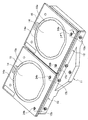
図1は、ウェハ保持装置10を模式的に示す斜視図であり、図2は、キャリア15を模式的に示す斜視図である。また、図3は、検査ステージ12および検査ステージ13において、初期高さ位置Bとされた支持面25(図4参照)にキャリア15が適切に載せられた状態のウェハ保持装置10を模式的に示す斜視図であり、図4は、図3のI−I線に沿って得られた断面図である。さらに、図5は、検査ステージ12および検査ステージ13において、分離高さ位置Eとされた支持面25(図6参照)にキャリア15が適切に載せられた状態のウェハ保持装置10を模式的に示す斜視図であり、図6は、図5のII−II線に沿って得られた断面図である。なお、図5では理解容易のためにウェハ14とキャリア15との上下方向で見た間隔を大きく取って示しているが、図6に示すように分離高さ位置Eとされた際にキャリア15とウェハ14とが間隔を置いていればよい。
FIG. 1 is a perspective view schematically showing the
ウェハ保持装置10は、図1に示すように、装置本体部11に設けられた検査ステージ12と検査ステージ13とを有する。ウェハ保持装置10は、本実施例では、ウェハ14の表面を検査する外観検査装置であり、ウェハ14が載置されたキャリア15を取り扱ってウェハ14を保持するものである。
As shown in FIG. 1, the
キャリア15は、図2に示すように、全体に矩形の板形状を呈し、中央に円形状の貫通孔15aが形成され、この貫通孔15aの周縁が段差状(図4の符号16および符号16a参照)とされて円板状のウェハ14の周縁部14a(図1、図3および図5参照)を下方から支えることで載置可能とする載置面16と、当該載置面16と直交する面に沿って延在し載置面16に載置されたウェハ14が載置面16に沿って移動することを防止する載置面直交壁部16aとを形成している。このようにウェハ14が載置されたキャリア15を、検査ステージ12および検査ステージ13(図1参照)で取り扱う。この検査ステージ12および検査ステージ13は、共にウェハ14を検査すべくキャリア15から分離してウェハ14を保持するものであり、同一の構成および動作であることから、検査ステージ12についてのみ説明をし、検査ステージ13に検査ステージ12と同じ符号を付して検査ステージ13の説明は省略する。なお、図1、図3および図5では、検査ステージ12および検査ステージ13で同時に同じ作業が行われているが、いずれか一方のみを動作させることも可能である。
As shown in FIG. 2, the
検査ステージ12は、キャリア15の環状空間15c(図2参照)への挿通が可能な円柱形状を呈するチャック台盤17と、このチャック台盤17を取り囲むように設けられた4つの吸着パッド18とを有する。チャック台盤17には、ウェハ受座19と台盤開放孔20とが設けられている。
The
ウェハ受座19は、チャック台盤17の上面17aの周縁部17bで全周に渡り上方へ立ち上がる環状の突条で構成されたリング状を呈し(図1、図4および図6参照)、その上面が水平な面とされて受け面21を構成している。以下では、受け面21に直交する方向を上下方向とする。
The
台盤開放孔20は、一端がウェハ受座19よりも内方でチャック台盤17の上面17aを開放しており、図示は略すが、他端が上面17a以外の個所でチャック台盤17の外部に開放している。このため、台盤開放孔20は、後述するように、ウェハ受座19の受け面21にウェハ14が適切に置かれることにより、ウェハ14とチャック台盤17の上面17aとウェハ受座19とにより区画された対向空間S(図4参照)を、ウェハ保持装置10が設置されている周囲に連通させてその大気圧と等しくすることができる。
One end of the base
ウェハ受座19には、複数のウェハ吸引孔23が設けられている。各ウェハ吸引孔23は、リング状のウェハ受座19を環状方向で見て所定の間隔を置きつつ点在して設けられており、図4および図6に示すように、一端が受け面21を開放し、他端が吸引装置Pに接続されている。ウェハ受座19では、その受け面21上にウェハ14が適切に置かれた状態において、吸引装置Pが各ウェハ吸引孔23の空気を吸引することにより、ウェハ14を吸着保持することができる。このことから、各ウェハ吸引孔23は、ウェハ受座19の受け面21および吸引装置Pと協働して、固定手段として機能している。このとき、ウェハ14の下方には、チャック台盤17(の上面17a)およびウェハ受座19とにより区画された対向空間Sが形成される。このウェハ受座19が、キャリア15に載置されたウェハ14を、キャリア15から分離しつつ吸着保持するために4つの吸着パッド18(図1参照)が設けられている。
The
各吸着パッド18は、弾性変形可能な部材から形成されており、上下方向への伸縮が自在とされた蛇腹状の筒状部材である。各吸着パッド18の下端18aは、検査ステージ12に設けられたキャリア支持台座24(後述する凹所底面24a)に気密的に取り付けられている。各吸着パッド18の上端18bは、上下方向に直交する同一の平面上に位置するように設定されており、キャリア15を下方から支持することができる支持面25を形成している。このため、各吸着パッド18の上端18bが形成する支持面25はウェハ受座19の受け面21と平行である。この各吸着パッド18の上端18bが形成する支持面25に適切にキャリア15が載せられると、各吸着パッド18の内方に形成された内方空間Iが封止される、すなわち各上端18bの開口が気密的に塞がれる。
Each
ここで、キャリア15が検査ステージ12上で適切な位置に置かれるということは、キャリア15が各吸着パッド18の上端18bが形成する支持面25に適切に載せられていることをいい、この状態のキャリア15に適切に載置されたウェハ14が上下方向に平行移動されるとウェハ受座19の受け面21に適切に置かれるように、互いの配置関係が設定されている。
Here, the
キャリア支持台座24には、キャリア15の位置決め穴15bに対応する位置決め突起24b(図1参照)が設けられており、支持面25により適切な位置で支持されたキャリア15が位置ずれすることが防止されている。また、キャリア支持台座24の上端面24cは、上下方向に直交する同一の平面上に位置するように設定されており、キャリア支持台座24には、上端面24cを開放しつつ収縮時の各吸着パッド18を収容するための凹所24dが設けられている。この凹所24dの底面である凹所底面24aに各吸着パッド18が気密的に取り付けられている。
The
各吸着パッド18は、外部からの負荷を受けていない状態において、形成する支持面25に支持されたキャリア15の載置面16がウェハ受座19の受け面21よりも上方に位置するように、すなわち支持面25にキャリア15が載せられた際当該キャリア15に載置されているウェハ14が受け面21から間隔を置いてその上方に位置するように、大きさ寸法が設定されており、このときの支持面25の高さ位置を初期高さ位置B(図4参照)とする。
Each
また、各吸着パッド18は、上端18bが協働して形成する支持面25に支持されたキャリア15の載置面16が、ウェハ受座19の受け面21よりも下方となりかつ凹所24dに収容される高さ位置まで収縮可能とされており、このときの支持面25の高さ位置を分離高さ位置E(図6参照)とする。各吸着パッド18は、外部からの負荷により支持面25が分離高さ位置Eとなるように収縮させることができるとともに、当該負荷が取り除かれると自らの復元力(弾性力)により元の大きさ寸法に戻り、支持面25が初期高さ位置Bとなる。
In addition, each
さらに、各吸着パッド18は、上端18bが協働して形成する支持面25にウェハ14が載置されたキャリア15が載せられると、そのキャリア15およびウェハ14の重さにより初期高さ位置Bに位置する支持面25が下方へ向けて緩やかに平行移動するように収縮し(矢印A1参照)、かつこの収縮により支持面25が後述するように受渡高さ位置T(図4参照)(分離高さ位置Eよりも上方)となってキャリア15のみを支える状態となると、支持面25が受渡高さ位置Tとなっている状態で伸縮しない強度(バネ力)となるように設定されている。
Further, when the
この各吸着パッド18の支持面25を分離高さ位置Eへ下降させるために、各キャリア支持台座24には、キャリア吸引孔26が設けられている。
In order to lower the
各キャリア吸引孔26は、一端が吸着パッド18の内方空間Iに連通するようにキャリア支持台座24の凹所底面24aを開放しており、他端が吸引装置Pに接続されている。本実施例では、各キャリア吸引孔26の他端と、各ウェハ吸引孔23の他端とには、単一の吸引装置Pが接続されている。また、図示は略すが、本実施例のウェハ保持装置10では、検査ステージ12と検査ステージ13とに単一の吸引装置Pが接続され、かつこの吸引装置Pに連通する吸引路が適宜選択的に開閉自在な構成とされており、単一の吸引装置Pで検査ステージ12と検査ステージ13とを同時にまたはいずれか一方のみを動作させることが可能とされている。
Each
支持面25に適切にキャリア15が載せられて各内方空間Iが封止された状態において、吸引装置Pが各内方空間Iの空気を吸引すると各内方空間Iが減圧されることから、キャリア15が各吸着パッド18に吸着保持されるとともに、伸縮自在とされた各吸着パッド18が収縮して各吸着パッド18の上端18bが形成する支持面25が下降して分離高さ位置Eに至る(図5および図6参照)。このことから、各吸着パッド18は、各キャリア吸引孔26および吸引装置Pと協働して、キャリア支持手段として機能している。
When the
次にウェハ保持装置10における動作について説明する。
Next, the operation in the
作業者は、ウェハ14が載置されたキャリア15を検査ステージ12(検査ステージ13でも同様)上へ持ってきて、キャリア支持手段としての各吸着パッド18の上端18bが形成し初期高さ位置Bに位置する支持面25に適切に載せる(図3および図4に2点鎖線で示す支持面25等参照)。すると、各吸着パッド18が形成する各内方空間Iが、キャリア15により密閉状態とされるとともに、ウェハ14が載置されたキャリア15の重さにより収縮し、支持面25が初期高さ位置Bから受渡高さ位置Tへと下方へ向けて下降(平行移動)する(図4に2点鎖線で示す矢印A1参照)。
The operator brings the
ここで、前述したように、各吸着パッド18は、支持面25が分離高さ位置E(図6参照)となる状態まで収縮可能とされており、かつウェハ受座19が設けられたチャック台盤17がキャリア15の環状空間15cに挿通可能とされていることから、支持面25が初期高さ位置B(図4参照)から分離高さ位置E(図6参照)へと変位される過程(各吸着パッド18の収縮過程)において、支持面25に載せられたキャリア15に載置されたウェハ14は、上方からウェハ受座19の受け面21に当接することとなる。ここで、キャリア15に載置されたウェハ14は、周縁部14aが載置面16により下方から支持されている状態、すなわち上方への移動が拘束されていない状態である。このため、ウェハ14は、キャリア15の載置面16がウェハ受座19の受け面21よりも下方へ移動されることにより、載置面16による支持から受け面21による支持へと、すなわちキャリア15に載置された状態からウェハ受座19に置かれた状態へと変わることとなる。このウェハ14がキャリア15に載置された状態からウェハ受座19に置かれた状態へと変わる際の各吸着パッド18の支持面25の高さ位置を受渡高さ位置T(図4参照)とする。すると、上述したように、各吸着パッド18は、受渡高さ位置T(図4参照)(分離高さ位置Eよりも上方)となってキャリア15のみを支える状態となると、支持面25が受渡高さ位置Tとなっている状態で伸縮しない強度(バネ力)となるように設定されていることから、キャリア15を受渡高さ位置Tで支えた状態で上下方向の移動を止まることとなる。このことから、支持面25が受渡高さ位置Tであるとき、キャリア15の載置面16は、ウェハ受座19の受け面21と同一平面上に位置するか、受け面21よりも僅かに下方に位置することとなる。
Here, as described above, each of the
ここで、キャリア15が支持面25に適切に載せられていることから、当該キャリア15に適切に載置されているウェハ14は、ウェハ受座19の受け面21に適切に置かれることとなる。この各吸着パッド18の支持面25が受渡高さ位置Tに位置し、かつウェハ受座19の受け面21に適切に置かれた状態において、ウェハ14は、受け面21により下方向への移動が制限され、上下方向と直交する面に沿う移動がキャリア15の載置面16を取り囲むように形成された載置面直交壁部16aにより制限されている(図4参照)。このため、例えウェハ保持装置10が移動されたとしてもウェハ14が受け面21上の適切な位置からずれることが防止されている。
Here, since the
その後、吸引装置Pを作動させ、キャリア15により密閉状態とされた各吸着パッド18が形成する各内方空間Iの空気および各ウェハ吸引孔23の空気を吸引する。すると、ウェハ受座19の受け面21に適切に置かれたウェハ14が、各ウェハ吸引孔23の空気の吸引によりウェハ受座19に吸着保持されるとともに、密閉状態とされた各内方空間Iが減圧されることにより、キャリア15が各吸着パッド18に吸着保持された状態で、伸縮自在とされた各吸着パッド18が収縮して各吸着パッド18の上端18bが形成する支持面25が、受渡高さ位置Tから下降し(図4矢印A2参照)、分離高さ位置Eに至る(図6参照)。このため、ウェハ保持装置10は、ウェハ14をキャリア15から分離して吸着保持することができ、かつ分離されたキャリア15も各吸着パッド18が形成する支持面25(分離高さ位置E)で吸着保持することができる。本実施例では、支持面25が分離高さ位置Eとなると、各吸着パッド18が凹所24dに収容され、キャリア15が、同一の平面上に位置するキャリア支持台座24の上端面24c上に載せられ、かつ上端面24c上に載せられたキャリア15の上面が、ウェハ受座19に吸着保持されたウェハ14の上面よりも下方に位置するように、設定されている。このことから、ウェハ保持装置10では、上下方向に直交する平面と平行な状態でかつ異なる高さ位置で、ウェハ14とキャリア15とを吸着保持することができる。
Thereafter, the suction device P is operated to suck the air in each inner space I and the air in each
このことから、吸引装置Pは、ウェハ受座19におけるウェハ14の吸着保持および各吸着パッド18におけるキャリア15の吸着保持を維持することができる程度に、各吸着パッド18が形成する内方空間Iの空気および各ウェハ吸引孔23の空気を吸引する設定とされている。
From this, the suction device P can maintain the suction space of the
検査ステージ12では、このように、ウェハ14とキャリア15とを分離して個別に吸着保持した状態で、ウェハ14に対する所望の作業(本実施例ではウェハ14上のチップ(図示せず)の外観検査)が行われる。本実施例の場合、図6に示すように、当該外観検査において、不適格とされたチップにインカー22(インクペン)で印(バッドマーク)を記載することとなるが、キャリア15の上面がウェハ14の上面よりも下方に位置されていることから、キャリア15がインカー22での印を記載する作業の妨げとなることを防止することができる。これは、次のことによる。インカー22は、印を記載する作業工程では、ウェハ14の上面から0.2mm〜0.5mmの高さ位置で、その上面に対して平行に相対的に移動され(矢印A3参照)、印をつける位置とされた際にペン先22aを上面へ向けて突出させる構成とされている。この印を記載する作業工程におけるインカー22のウェハ14の上面での相対的な平行移動は、必ずしもウェハ14の上方のみで行われるものではなく、キャリア15の上方に位置される場合(矢印A3および2点鎖線で示すインカー22参照)がある。このことから、キャリア15の上面がウェハ14の上面よりも上方に位置されていると、インカー22とキャリア15とが干渉してしまう虞があることによる。
In the
その後、保持した状態でのウェハ14に対する所望の作業が終了すると、ウェハ受座19におけるウェハ14の吸着保持および各吸着パッド18におけるキャリア15の吸着保持を解除すべく吸引装置Pが動作され、各吸着パッド18の復元力によりその上端18bが形成する支持面25が分離高さ位置E(図6参照)から受渡高さ位置Tを経て初期高さ位置B(図4参照)へと上昇される。
Thereafter, when a desired operation on the
この上昇過程において、上昇するキャリア15の載置面16がウェハ受座19における吸着保持が解除されたウェハ14に下方から当接し(受渡高さ位置T)、受け面21がウェハ14を支持する状態から載置面16がウェハ14を支持する状態へと変わり、キャリア15の載置面16にウェハ14が適切に載置されることとなる。このため、図4に示すように、各吸着パッド18の上端18bが形成する支持面25が受渡高さ位置Tとされると、この支持面25には、載置面16にウェハ14を載置した状態のキャリア15が適切に載せられていることとなる。この後、キャリア15を各吸着パッド18の支持面25上から降ろす(取り去る)ことにより、再びキャリア15に適切に載置されたウェハ14を取り扱うことができる。これにより、各吸着パッド18は、復元力(弾性力)により元の大きさ寸法に戻り、支持面25が再び初期高さ位置Bとなる。
In this ascending process, the mounting
上記したように、ウェハ保持装置10では、キャリア15に載置されたウェハ14を、キャリア15から分離してウェハ受座19の受け面21で吸着保持することができ、かつこの分離から吸着保持の過程において、キャリア15の載置面16およびウェハ受座19の受け面21以外の物体をウェハ14に接触させることはない。ここで、キャリア15の載置面16は、他の場面においても搬送等の際に接触する個所であり、かつウェハ受座19の受け面21は、吸着保持される個所であることから、ウェハ保持装置10では、必要最低限の接触のみでウェハ14を適切に吸着保持することができることとなる。
As described above, in the
また、ウェハ保持装置10では、ウェハ14とキャリア15とを分離して個別に吸着保持した状態から、ウェハ受座19の受け面21以外の物体をウェハ14に接触させることなく、ウェハ14をキャリア15の載置面16に適切に載置することができる。このため、ウェハ保持装置10を用いてウェハ14に対する所望の作業(本実施例ではウェハ14上のチップ(図示せず)の外観検査)を行う場合、キャリア15の載置面16に適切に載置された状態でウェハ14を取り扱えばよい、すなわちキャリア15を取り扱えばよいこととなるので、作業者がウェハ14に触れる必要がなく、ウェハ14がキャリア15の載置面16を除く他の物体に接触する機会が生じることを防止することができる。
Further, in the
さらに、ウェハ保持装置10では、作業者はキャリア15を取り扱えばよいことから、ウェハ14を取り扱うことに比較して慎重さが求められることはなく、ウェハ14に対する所望の作業(本実施例ではウェハ14上のチップ(図示せず)の外観検査)のための準備時間を短縮することができるとともに、当該準備の際にウェハ14を汚してしまったり傷つけてしまったりすることを防止することができる。
Further, in the
ウェハ保持装置10では、ウェハ14とキャリア15とを分離してそれぞれ吸着保持した状態で、ウェハ14に対する所望の作業(本実施例ではウェハ14上のチップ(図示せず)の外観検査)を行うことができるので、キャリア15が移動してしまうことで当該作業の妨げとなることを防止することができるとともに、キャリア15が移動してしまうことに伴って生じ得る発塵を防止することができる。
In the
ウェハ保持装置10では、各キャリア吸引孔26の他端および各ウェハ吸引孔23の他端に単一の吸引装置Pが接続されていることから、単一の吸引装置Pを動力源として、ウェハ受座19でのウェハ14の保持と、キャリア支持手段の支持面25の上下方向の移動と、キャリア15の吸着保持とを行うことができる。
In the
ウェハ保持装置10では、キャリア15の載置面16を上下方向に移動させてウェハ受座19の受け面21との間でウェハ14の受け渡し(載置面16に載置された状態と受け面21に置かれた状態との入れ換え)を行う構成であることから、ウェハを保持して載置面と受け面との間を移動させることに比較して、ウェハ14を汚してしまったり傷つけてしまったりすることを防止することができる。
In the
ウェハ保持装置10では、キャリア15の載置面16を上下方向に移動させてウェハ受座19の受け面21との上下関係を逆転させることにより、載置面16と受け面21との間でウェハ14を受け渡す構成であることから、受け面21と載置面16との相対的な高さ位置に誤差が生じていても確実にウェハ14を保持することができる。これに対し、例えば、キャリアの載置面に載置された状態のウェハを当該キャリアと一体的に保持する構成である場合、受け面と載置面との相対的な高さ位置がウェハの確実な保持に影響を及ぼす、すなわち載置面が高い場合ウェハをウェハ受座の受け面に吸着保持させることができず、受け面が高い場合そこに吸着保持される前にキャリアの載置面からウェハが飛び出してしまうことから、受け面と載置面との相対的な高さ位置に誤差によりウェハの保持が阻害されてしまう。
In the
ウェハ保持装置10では、初期高さ位置Bに位置する支持面25にウェハ14が載置されたキャリア15が載せられると、その重さにより支持面25が緩やかに下降することにより、キャリア15の載置面16からウェハ受座19の受け面21へとウェハ14を受け渡す構成であることから、ウェハ14を汚してしまったり傷つけてしまったりすることを防止することができる。
In the
ウェハ保持装置10では、チャック台盤17には台盤開放孔20が設けられていることから、ウェハ14がウェハ受座19に吸着保持されているとき、ウェハ14とチャック台盤17の上面17aとの間に形成された対向空間Sが、各ウェハ吸引孔23の空気の吸引に伴って負圧となることを防止することができる。このことから、対向空間Sが負圧となることに起因してウェハ14に撓みが生じることを防止することができる。
In the
ウェハ保持装置10では、ウェハ14およびキャリア15を分離した状態で各々吸着保持している際、キャリア15の上面がウェハ14の上面よりも下方に位置されていることから、キャリア15がウェハ14に対して為される所望の作業(上記した実施例ではウェハ14上のチップ(図示せず)の外観検査であり、一例としてチップにインカー22での印を記載する作業)の妨げとなることを防止することができる。
In the
ウェハ保持装置10では、各吸着パッド18の支持面25が受渡高さ位置Tとされ、かつウェハ14がウェハ受座19の受け面21に適切に置かれた状態において、ウェハ14が受け面21により下方向への移動が制限され、かつ載置面直交壁部16aにより上下方向と直交する面に沿う移動が制限されていることから、吸引装置Pを作動させる前(吸着保持していない状態)であっても、ウェハ14が受け面21上の適切な位置からずれることを防止することができる。
In the
ウェハ保持装置10では、検査ステージ12と検査ステージ13との2箇所で、ウェハ14をキャリア15から分離しつつ適切に吸着保持することができるので、ウェハ14に対して為される所望の作業(上記した実施例ではウェハ14上のチップ(図示せず)の外観検査)を効率良く行うことができる。
In the
ウェハ保持装置10では、単一の吸引装置Pで、検査ステージ12および検査ステージ13においてウェハ14をキャリア15から分離しつつ適切に吸着保持することができる。換言すると、検査ステージ12におけるウェハ14の吸着保持、そのウェハ14とキャリア15との分離およびキャリア15の吸着保持と、検査ステージ13におけるウェハ14の吸着保持、そのウェハ14とキャリア15との分離およびキャリア15の吸着保持とを、単一の吸引装置Pを動力源として行うことができる。
In the
したがって、本実施例に係るウェハ保持装置10では、キャリア15に載置されているウェハ14を、他の物体と接触する機会を増加させることなく保持することができる。
Therefore, in the
なお、上記した実施例では、吸引装置Pによるウェハ吸引孔23の空気を吸引することによりウェハ受座19でウェハ14を吸着保持するもの(固定手段)とされていたが、ウェハ14をウェハ受座19に固定することができるものであれば、例えば、複数の保持爪がウェハ受座にウェハを固定する構成(固定手段)であってもよく、上記した実施例に限定されるものではない。
In the above-described embodiment, the
また、上記した実施例では、ウェハ保持装置10は、ウェハ14上のチップ(図示せず)の外観検査を行うものであったが、例えば、光を照射することによりウェハの表面に成膜または塗布された光感光剤(フォトレジスト)に回路パターンを露光・転写する半導体露光装置、ウェハを保持した状態で搬送するウェハ搬送装置等に用いてもよく、上記した実施例に限定されるものではない。
In the above-described embodiment, the
さらに、上記した実施例では、各吸着パッド18、各キャリア吸引孔26および吸引装置Pによりキャリア支持手段が構成されていたが、キャリアを支持する支持面を上下方向に移動させることにより、キャリアの載置面とウェハ受座の受け面との上下関係を逆転させて載置面と受け面との間でウェハを受け渡すことができるものであればよく、上記した実施例に限定されるものではない。
Further, in the above-described embodiment, the carrier support means is constituted by each
上記した実施例では、各キャリア吸引孔26の他端と各ウェハ吸引孔23の他端とには単一の吸引装置Pが接続されていたが、それぞれ個別に吸引装置を設ける構成であってもよく、上記した実施例に限定されるものではない。
In the above-described embodiment, the single suction device P is connected to the other end of each
上記した実施例では、各吸着パッド18の上端18bが形成する支持面25に適切にキャリア15が載せられると各吸着パッド18の内方空間Iが封止されることにより各吸着パッド18形成する支持面25で吸着保持することができる構成とされていたが、例えば、各吸着パッドの上端に板部材を設けて、この板部材の上面を支持面とするものであってもよい。この場合、ウェハから分離したキャリアを吸着保持することができなくなるが、単一の吸引装置を動力源として、ウェハ受座でのウェハの保持と、キャリア支持手段の支持面の上下方向の移動とを行うことができる。
In the above-described embodiment, when the
10 ウェハ保持装置
11 装置本体部
12 検査ステージ
13 検査ステージ
14 ウェハ
14a 周縁部
15 キャリア
15c 環状空間
17 チャック台盤
17b 周縁部
18 (筒状部材としての)吸着パッド
18b 上端
19 ウェハ受座
21 受け面
23 ウェハ吸引孔
26 (キャリア支持手段であり吸引機構としての)キャリア吸引孔
B 初期高さ位置
P (キャリア支持手段であり吸引機構としての)吸引装置
DESCRIPTION OF
Claims (5)
前記ウェハは、前記ウェハ受座に固定される前は前記ウェハの周縁部を下方から支持する環状を呈しその環状空間で前記チャック台盤を受け入れ可能とされたキャリアに載置されており、
前記装置本体部は、前記ウェハ受座の受け面と前記ウェハとが平行な状態で前記キャリアを支持可能な支持面を形成し、かつ該支持面の高さ位置を前記受け面と直交する方向に変位自在であり、さらに前記支持面に前記キャリアが載せられた状態では前記ウェハを前記ウェハ受座に当接させる受渡高さ位置に前記支持面を位置させるキャリア支持手段を有し、
前記受渡高さ位置の前記支持面に載せられている前記キャリアに載置されて前記ウェハ受座に置かれた前記ウェハを前記固定手段で固定することに伴って、前記キャリア支持手段が前記支持面を前記受渡高さ位置から下降させて前記ウェハを前記キャリアから分離することを特徴とするウェハ保持装置。 A ring-shaped wafer seat is formed along the peripheral edge of a columnar chuck base provided in the apparatus main body, and the peripheral edge of the wafer placed on the wafer seat is fixed to the wafer receiver by a plurality of fixing means. A wafer holding device capable of holding the wafer by being fixed to
Before the wafer is fixed to the wafer seat, the wafer is mounted on a carrier that has an annular shape that supports the peripheral edge of the wafer from below and is capable of receiving the chuck base in the annular space.
The apparatus main body forms a support surface capable of supporting the carrier in a state where the receiving surface of the wafer seat and the wafer are parallel, and the height position of the support surface is orthogonal to the receiving surface. The carrier support means for positioning the support surface at a delivery height position for contacting the wafer to the wafer seat when the carrier is placed on the support surface.
The carrier support means supports the wafer as the wafer placed on the carrier placed on the support surface at the delivery height position and placed on the wafer seat is fixed by the fixing means. A wafer holding device, wherein the wafer is separated from the carrier by lowering a surface from the delivery height position.
前記筒状部材は、前記初期高さ位置にある前記支持面に前記キャリアが載せられると該キャリアの重さにより前記支持面を前記初期高さ位置から前記受渡高さ位置まで下降させ、前記吸引機構の吸引により前記支持面を前記受渡高さ位置から下降させることを特徴とする請求項2に記載のウェハ保持装置。 The carrier support means is formed of an elastically deformable member and has a bellows shape that can be expanded and contracted. A cylindrical member provided in the apparatus main body, and air in an inner space of the cylindrical member is supplied to the apparatus main body side. And a suction mechanism capable of sucking
When the carrier is placed on the support surface at the initial height position, the cylindrical member lowers the support surface from the initial height position to the delivery height position by the weight of the carrier, and the suction member The wafer holding apparatus according to claim 2, wherein the support surface is lowered from the delivery height position by suction of a mechanism.
The fixing means has a wafer suction hole that opens the receiving surface, can be sealed by placing the wafer on the wafer seat, and can suck air by the suction mechanism. The wafer holding apparatus according to claim 3 or 4, wherein
Priority Applications (4)
| Application Number | Priority Date | Filing Date | Title |
|---|---|---|---|
| JP2007277162A JP4857239B2 (en) | 2007-10-25 | 2007-10-25 | Wafer holding device |
| US12/288,284 US7923990B2 (en) | 2007-10-25 | 2008-10-17 | Wafer holder |
| KR1020080104839A KR100998552B1 (en) | 2007-10-25 | 2008-10-24 | Wafer holder |
| TW097140908A TW200919626A (en) | 2007-10-25 | 2008-10-24 | Wafer holder |
Applications Claiming Priority (1)
| Application Number | Priority Date | Filing Date | Title |
|---|---|---|---|
| JP2007277162A JP4857239B2 (en) | 2007-10-25 | 2007-10-25 | Wafer holding device |
Publications (3)
| Publication Number | Publication Date |
|---|---|
| JP2009105295A JP2009105295A (en) | 2009-05-14 |
| JP2009105295A5 JP2009105295A5 (en) | 2010-12-02 |
| JP4857239B2 true JP4857239B2 (en) | 2012-01-18 |
Family
ID=40583061
Family Applications (1)
| Application Number | Title | Priority Date | Filing Date |
|---|---|---|---|
| JP2007277162A Expired - Fee Related JP4857239B2 (en) | 2007-10-25 | 2007-10-25 | Wafer holding device |
Country Status (4)
| Country | Link |
|---|---|
| US (1) | US7923990B2 (en) |
| JP (1) | JP4857239B2 (en) |
| KR (1) | KR100998552B1 (en) |
| TW (1) | TW200919626A (en) |
Cited By (1)
| Publication number | Priority date | Publication date | Assignee | Title |
|---|---|---|---|---|
| CN107039308A (en) * | 2015-10-22 | 2017-08-11 | 朗姆研究公司 | Front open type ring box |
Families Citing this family (6)
| Publication number | Priority date | Publication date | Assignee | Title |
|---|---|---|---|---|
| JP2011029217A (en) * | 2009-07-21 | 2011-02-10 | Okawa Kanagata Sekkei Jimusho:Kk | Holder for wafer |
| WO2011074274A1 (en) * | 2009-12-18 | 2011-06-23 | 株式会社ニコン | Pair of substrate holders, method for manufacturing device, separation device, method for separating substrates, substrate holder, and device for positioning substrate |
| RU2523356C2 (en) * | 2012-10-16 | 2014-07-20 | Федеральное государственное бюджетное образовательное учреждение высшего профессионального образования "Новгородский государственный университет имени Ярослава Мудрого" | Electrode structure for electrocardiogram |
| TW201714243A (en) * | 2015-10-05 | 2017-04-16 | Els System Technology Co Ltd | Carrying device capable of carrying and moving a wafer upward and downward for providing more usage flexibility |
| JP6842948B2 (en) * | 2017-02-24 | 2021-03-17 | リンテック株式会社 | Positioning device and positioning method |
| ES2884373T3 (en) * | 2017-06-28 | 2021-12-10 | Meyer Burger Germany Gmbh | Device for the transport of a substrate, a treatment device with a housing plate adapted to a substrate support of such a device and a procedure for the processing of a substrate using such a device for the transport of a substrate, as well as a treatment plant |
Family Cites Families (5)
| Publication number | Priority date | Publication date | Assignee | Title |
|---|---|---|---|---|
| JPH07201948A (en) * | 1993-12-29 | 1995-08-04 | Dainippon Screen Mfg Co Ltd | Substrate transferring jig |
| US6137303A (en) * | 1998-12-14 | 2000-10-24 | Sony Corporation | Integrated testing method and apparatus for semiconductor test operations processing |
| JP4128023B2 (en) * | 2002-04-26 | 2008-07-30 | 株式会社トプコン | Wafer holding device |
| JP4471747B2 (en) * | 2004-06-24 | 2010-06-02 | アピックヤマダ株式会社 | Semiconductor device manufacturing equipment |
| JP2007109771A (en) * | 2005-10-12 | 2007-04-26 | Matsushita Electric Ind Co Ltd | Tray for plasma treatment apparatus |
-
2007
- 2007-10-25 JP JP2007277162A patent/JP4857239B2/en not_active Expired - Fee Related
-
2008
- 2008-10-17 US US12/288,284 patent/US7923990B2/en not_active Expired - Fee Related
- 2008-10-24 KR KR1020080104839A patent/KR100998552B1/en not_active IP Right Cessation
- 2008-10-24 TW TW097140908A patent/TW200919626A/en unknown
Cited By (2)
| Publication number | Priority date | Publication date | Assignee | Title |
|---|---|---|---|---|
| CN107039308A (en) * | 2015-10-22 | 2017-08-11 | 朗姆研究公司 | Front open type ring box |
| CN107039308B (en) * | 2015-10-22 | 2020-01-03 | 朗姆研究公司 | Front-opening type ring box |
Also Published As
| Publication number | Publication date |
|---|---|
| US7923990B2 (en) | 2011-04-12 |
| US20090110521A1 (en) | 2009-04-30 |
| KR20090042191A (en) | 2009-04-29 |
| KR100998552B1 (en) | 2010-12-07 |
| TW200919626A (en) | 2009-05-01 |
| JP2009105295A (en) | 2009-05-14 |
Similar Documents
| Publication | Publication Date | Title |
|---|---|---|
| JP4857239B2 (en) | Wafer holding device | |
| JP6486140B2 (en) | Conveying hand, lithographic apparatus, and method for conveying an object to be conveyed | |
| JP6535206B2 (en) | Exposure method and exposure apparatus | |
| KR102134207B1 (en) | Holder, lithography apparatus, method of manufacturing article, and stage apparatus | |
| US20080068580A1 (en) | Substrate-retaining unit | |
| CN108983553B (en) | Transfer hand, transfer apparatus, lithographic apparatus, method of manufacturing article, and holding mechanism | |
| TW200402823A (en) | Method and device for holding reticle and exposure device | |
| JP3441956B2 (en) | Exposure apparatus, cleaning grindstone and device manufacturing method | |
| JPH03270048A (en) | Vacuum chuck | |
| JP2613035B2 (en) | Substrate suction fixing device | |
| JP2012009720A (en) | Wafer holder and exposure equipment | |
| JP2015041777A (en) | Fluorescent film pickup device for led chip | |
| KR20140120822A (en) | Chuck table | |
| JP2014241357A (en) | Substrate holding device, optical device, and substrate holding method | |
| JP4447497B2 (en) | Board holder | |
| KR101619876B1 (en) | Suction pad for transferring device and the transferring device comprising the same | |
| JP7222535B2 (en) | Work transfer hand and ball mounting device | |
| JP2021158329A (en) | Stamp tool holding device and manufacturing method of element array | |
| JP2010140921A (en) | Device and method for mounting ball, and apparatus for manufacturing electronic component | |
| JP2008251944A (en) | Exposure apparatus | |
| JP5495094B2 (en) | Contact exposure apparatus and contact exposure method | |
| JP6844804B1 (en) | Exposure device and exposure method | |
| JP2006324312A (en) | Substrate-holding device | |
| KR102418538B1 (en) | Substrate Holding Device | |
| JPH0661334A (en) | Wafer transfer machine |
Legal Events
| Date | Code | Title | Description |
|---|---|---|---|
| A521 | Request for written amendment filed |
Free format text: JAPANESE INTERMEDIATE CODE: A523 Effective date: 20101018 |
|
| A621 | Written request for application examination |
Free format text: JAPANESE INTERMEDIATE CODE: A621 Effective date: 20101018 |
|
| A977 | Report on retrieval |
Free format text: JAPANESE INTERMEDIATE CODE: A971007 Effective date: 20110916 |
|
| TRDD | Decision of grant or rejection written | ||
| A01 | Written decision to grant a patent or to grant a registration (utility model) |
Free format text: JAPANESE INTERMEDIATE CODE: A01 Effective date: 20111004 |
|
| A01 | Written decision to grant a patent or to grant a registration (utility model) |
Free format text: JAPANESE INTERMEDIATE CODE: A01 |
|
| A61 | First payment of annual fees (during grant procedure) |
Free format text: JAPANESE INTERMEDIATE CODE: A61 Effective date: 20111031 |
|
| FPAY | Renewal fee payment (event date is renewal date of database) |
Free format text: PAYMENT UNTIL: 20141104 Year of fee payment: 3 |
|
| R150 | Certificate of patent or registration of utility model |
Free format text: JAPANESE INTERMEDIATE CODE: R150 |
|
| LAPS | Cancellation because of no payment of annual fees |