JP4850423B2 - Nitride semiconductor device - Google Patents
Nitride semiconductor device Download PDFInfo
- Publication number
- JP4850423B2 JP4850423B2 JP2005039387A JP2005039387A JP4850423B2 JP 4850423 B2 JP4850423 B2 JP 4850423B2 JP 2005039387 A JP2005039387 A JP 2005039387A JP 2005039387 A JP2005039387 A JP 2005039387A JP 4850423 B2 JP4850423 B2 JP 4850423B2
- Authority
- JP
- Japan
- Prior art keywords
- nitride semiconductor
- semiconductor layer
- layer
- electrode
- semiconductor device
- Prior art date
- Legal status (The legal status is an assumption and is not a legal conclusion. Google has not performed a legal analysis and makes no representation as to the accuracy of the status listed.)
- Expired - Fee Related
Links
Images


Landscapes
- Junction Field-Effect Transistors (AREA)
Description
本発明は、能動層に窒化物半導体を用いた窒化物半導体装置に関し、特に高電子移動度トランジスタ(HEMT:High Electron Mobility Transistor)や電界効果トランジスタ(FET:Field Effect Transistor)のような、半導体装置にショットキ接触する制御電極を有し、インバーターやコンバーターなどのスイッチング装置に応用されるノーマリーオフ型の電界効果トランジスタ等に関する。 The present invention relates to a nitride semiconductor device using a nitride semiconductor as an active layer, and in particular, a semiconductor device such as a high electron mobility transistor (HEMT) or a field effect transistor (FET). The present invention relates to a normally-off type field effect transistor having a control electrode in Schottky contact and applied to a switching device such as an inverter or a converter.
図6は、従来のIII−V族窒化物半導体からなる半導体装置の断面図を示している。図6に示す半導体装置は、いわゆるHEMT構造を示しており、サファイア基板からなる基板101上には、窒化ガリウム(GaN)からなるバッファ層102、窒化ガリウムからなるチャネル層103、n型窒化アルミニウムガリウム(AlGaN)からなるキャリア供給層104、ノンドープの窒化アルミニウムガリウムからなるショットキ層105が順次積層した構造となっており、チャネル層103とキャリア供給層104とからなるヘテロ接合界面近傍に、ポテンシャル井戸からなる電子移動度が極めて大きい2次元電子ガス層が形成されている。ショットキ層105には凹部105aを形成し、この凹部105a内にショットキ接触するゲート電極106(制御電極)を形成している。このような構造の半導体装置では、ゲート電極106に印加する電圧を制御することにより、ソース電極107aとドレイン電極107bとの間を流れるキャリア(2次元電子ガス)を制御している。また凹部105aを備えることにより、ピンチオフ電圧を浅くしている。即ち、ゲート電極106に印加する制御電圧が0Vのとき、ゲート電極106直下のチャネルにはキャリアが存在せず、ゲート電極106直下以外のチャネルにキャリアが存在しているノーマリーオフ型となっている。
FIG. 6 shows a cross-sectional view of a conventional semiconductor device made of a group III-V nitride semiconductor. The semiconductor device shown in FIG. 6 has a so-called HEMT structure, on a
図7は、別の従来例のIII−V族窒化物半導体からなる半導体装置の断面図を示している。図7に示す半導体装置は、図6で説明した凹部105bの代わりに、ショットキ層105上にp型不純物をドープしたp型窒化ガリウム層105bを形成し、p型窒化ガリウム層105b上にゲート電極106を形成している。このような構造の半導体装置では、p型窒化ガリウム
層105bとノンドープの窒化アルミニウムガリウムからなるショットキ層105との間で形成されるビルトインポテンシャルを利用することにより、ピンチオフ電圧を浅くし、ノーマリーオフ型となっている(たとえば非特許文献1等)。
図6に示すショットキ層105に凹部105aを形成し、この凹部105a内にゲート電極106を形成する従来の窒化物半導体装置では、ショットキ層105をドライエッチングすることで凹部105aを形成するため、その表面にダメージを与えてしまう。即ち、ゲート電極106がショットキ接触するショットキ層105の表面にダメージを与えてしまうことになる。その結果、ショットキ障壁高さが小さくなり、完全なノーマリーオフ型の動作が実現できないという問題があった。
In the conventional nitride semiconductor device in which the
また、図7に示すショットキ層105上にp型窒化ガリウム層105bを備える構造では、窒化ガリウム層にp型不純物を高濃度にドープすることが困難であり、その活性化率も低いため、高濃度のp型窒化ガリウム層105bを形成することができず、良好なpn接合を形成できなかった。その結果、ビルトインポテンシャルが小さくなり、完全なノーマリーオフ型の動作が実現できないという問題があった。
Further, in the structure including the p-type
本発明は、完全なノーマリーオフ型動作を実現することができる、窒化物半導体装置を提供することを目的とする。 An object of the present invention is to provide a nitride semiconductor device capable of realizing a completely normally-off operation.
上記目的を達成するため、本願請求項1に係る発明は、基板上に積層したガリウム、アルミニウム、ホウ素及びインジウムからなる群のうち少なくとも1つからなるIII族元素と、窒素、リン及び砒素からなる群のうちの少なくとも窒素を含むV族元素で構成されたIII−V族窒化物半導体層からなる第1の窒化物半導体層と、該第1の窒化物半導体層の上に積層した前記III−V族窒化物半導体層からなり、アルミニウムを含まない第2の窒化物半導体層と、該第2の窒化物半導体層にショットキ接触する制御電極とを備え、前記第2の窒化物半導体層は、微結晶構造からなる窒化物半導体装置において、前記制御電極に印加する制御電圧が0Vのとき、前記制御電極直下の前記第1の窒化物半導体層からなるチャネルにキャリアが存在せず、前記制御電極直下以外の前記チャネルにキャリアが存在していることを特徴とするものである。 In order to achieve the above object, the invention according to claim 1 of the present application comprises a group III element consisting of at least one of the group consisting of gallium, aluminum, boron and indium laminated on a substrate, and nitrogen, phosphorus and arsenic. A first nitride semiconductor layer comprising a group III-V nitride semiconductor layer composed of a group V element containing at least nitrogen in the group; and the III- layer laminated on the first nitride semiconductor layer. A second nitride semiconductor layer made of a group V nitride semiconductor layer and containing no aluminum, and a control electrode in Schottky contact with the second nitride semiconductor layer, wherein the second nitride semiconductor layer comprises: in the nitride semiconductor device comprising a microcrystalline structure, when the control voltage applied to the control electrode of 0V, there is no carrier in the first channel made of a nitride semiconductor layer immediately below the control electrode, before It is characterized in that the carrier in the channel other than directly below the control electrodes are present.
請求項2に係る発明は、請求項1に記載の窒化物半導体装置において、前記基板と前記第1の窒化物半導体層との間に、前記第1の窒化物半導体層のエネルギーギャップより小さいエネルギーギャップを持つ、前記III−V族窒化物半導体層からなる第3の窒化物半導体層を備え、前記制御電極に印加する制御電圧が0Vのとき、前記制御電極直下の前記第3の窒化物半導体層と前記第1の窒化物半導体層との間に形成されるチャネルにキャリアが存在せず、前記制御電極直下以外の前記チャネルにキャリアが存在していることを特徴とするものである。 According to a second aspect of the present invention, in the nitride semiconductor device according to the first aspect, an energy smaller than an energy gap of the first nitride semiconductor layer is provided between the substrate and the first nitride semiconductor layer. with gaps, a third nitride semiconductor layer made of the group III-V nitride semiconductor layer, when the control voltage applied to the control electrode of 0V, the third nitride semiconductor directly under the control electrode A carrier is not present in a channel formed between a layer and the first nitride semiconductor layer, and a carrier is present in the channel other than immediately below the control electrode.
請求項3に係る発明は、請求項1又は2いずれかに記載の窒化物半導体装置において、前記第2の窒化物半導体層にショットキ接触する前記制御電極と、前記第1の窒化物半導体層にオーミック接触するソース電極及びドレイン電極とを備え、前記第1の窒化物半導体層からなるチャネル、あるいは前記第3の窒化物半導体層と前記第1の窒化物半導体層との間に形成されるチャネルを流れる電流を前記制御電極に印加する電圧により制御することを特徴とするものである。 According to a third aspect of the present invention, in the nitride semiconductor device according to the first or second aspect, the control electrode in Schottky contact with the second nitride semiconductor layer, and the first nitride semiconductor layer A channel having a source electrode and a drain electrode that are in ohmic contact, and a channel formed of the first nitride semiconductor layer or a channel formed between the third nitride semiconductor layer and the first nitride semiconductor layer The current flowing through is controlled by the voltage applied to the control electrode .
請求項4に係る発明は、請求項1乃至3いずれかに記載の窒化物半導体装置において、前記第2の窒化物半導体層上にオーミック接触する電極を備え、該電極は、成膜状態の前記第2の窒化物半導体層に接触していることを特徴とするものである。 The invention according to claim 4 is the nitride semiconductor device according to any one of claims 1 to 3, further comprising an electrode in ohmic contact with the second nitride semiconductor layer, wherein the electrode is in the film-formed state. The second nitride semiconductor layer is in contact with the second nitride semiconductor layer .
本発明による窒化物半導体装置は、少なくともアルミニウムを含まず、エピタキシャル成長温度を通常の温度より低く設定して微結晶構造とした絶縁性の高い窒化物半導体層に制御電極を接触させる構造とすることにより、制御電極と窒化物半導体層との間で形成されるショットキ障壁の高さを、従来の窒化物半導体層との接触に比べて高くすることができる。その結果、本発明の制御電極をFETあるいはHEMT等のゲート電極とし、ソース−ゲート電極間の電位差が0Vとなるように制御電圧を印加した場合、ゲート電極直下のチャネルにキャリアが存在せず、ゲート電極直下以外の領域であるゲート−ソース電極間、ゲート−ドレイン電極間のチャネルにはキャリアが存在する構造を形成することができ、ノーマリーオフ型の動作を実現する窒化物半導体装置を提供することが可能となる。 The nitride semiconductor device according to the present invention has a structure in which at least aluminum is not contained and the control electrode is brought into contact with a highly insulating nitride semiconductor layer having a microcrystalline structure by setting an epitaxial growth temperature lower than a normal temperature. The height of the Schottky barrier formed between the control electrode and the nitride semiconductor layer can be made higher than that of the contact with the conventional nitride semiconductor layer. As a result, when the control electrode of the present invention is a gate electrode such as an FET or HEMT and a control voltage is applied so that the potential difference between the source and gate electrodes is 0 V, no carriers are present in the channel immediately below the gate electrode, Provided is a nitride semiconductor device capable of forming a structure in which carriers exist in a channel between a gate and a source electrode and a channel between a gate and a drain electrode, which are regions other than directly under the gate electrode, and realizing a normally-off type operation. It becomes possible to do.
本発明の制御電極は、絶縁性の高い微結晶構造からなる窒化物半導体層上に設けられるため、リーク電流を少なくすることができる。本発明の制御電極をFETあるいはHEMT等のゲート電極とした場合、ゲートリーク電流が減少する。さらにチャネルでの衝突イオン化が抑制されることにより、高耐圧化を実現できる。またゲート−ドレイン電極の間に絶縁性の高い微結晶構造からなる窒化物半導体層が設けられている構造とするため、ゲート−ドレイン電極の間の表面準位にトラップされる電子の抑制若しくは表面準位密度の低減により電流コラプス現象が抑制され、高周波特性も改善される。 Since the control electrode of the present invention is provided on a nitride semiconductor layer having a highly crystalline microcrystalline structure, leakage current can be reduced. When the control electrode of the present invention is a gate electrode such as an FET or HEMT, the gate leakage current is reduced. Further, by suppressing collision ionization in the channel, a high breakdown voltage can be realized. In addition, since a nitride semiconductor layer having a highly insulating microcrystalline structure is provided between the gate and drain electrodes, suppression of electrons trapped in the surface level between the gate and drain electrodes or the surface By reducing the level density, the current collapse phenomenon is suppressed and the high frequency characteristics are improved.
本発明によれば、アルミニウムを含まず、不純物イオンの注入等の加工を施さない成膜後の、微結晶構造のままの窒化物半導体層上にオーミック電極を形成することにより、窒化物半導体の微結晶粒界にオーミック電極を構成する金属が侵入し、コンタクト抵抗率の低い(10-6Ω・cm2台)オーミック電極を備えた半導体装置を得ることができる。 According to the present invention, an ohmic electrode is formed on a nitride semiconductor layer having a microcrystalline structure after film formation that does not include aluminum and is not subjected to processing such as implantation of impurity ions. A semiconductor device having an ohmic electrode with low contact resistivity (10 −6 Ω · cm 2 ) can be obtained because the metal constituting the ohmic electrode penetrates into the crystal grain boundary.
以下、本発明の窒化物半導体装置について、詳細に説明する。 Hereinafter, the nitride semiconductor device of the present invention will be described in detail.
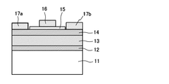
まず本発明の窒化物半導体装置について、III−V族窒化物半導体装置であるHEMTを例にとり、詳細に説明する。図1は本発明の第1の実施例である。図1に示すように炭化珪素(SiC)からなる基板11上に、厚さ100nm程度の窒化アルミニウム(AlN)からなるバッファ層12、後述するキャリア供給層のエネルギーギャップより小さいエネルギーギャップを持ち、厚さ2μmのノンドープ窒化ガリウム(GaN)からなるチャネル層13、チャネル層13との界面にキャリアとなる2次元電子ガス層を形成する厚さ15nmのノンドープ窒化アルミニウムガリウム(AlGaN)からなるキャリア供給層14、厚さ10nmの微結晶構造のノンドープ窒化ガリウム(GaN)からなるショットキ層15を積層形成している。ショットキ層15上には、ニッケル(Ni)/金(Au)の積層体等からなるゲート電極16を形成し、ショットキ層15との間にショットキ接触を形成している。更にショットキ層15の一部が除去され、キャリア供給層14にオーミック接触するチタン(Ti)/アルミニウム(Al)からなるソース電極17a、ドレイン電極17bを形成している。
First, the nitride semiconductor device of the present invention will be described in detail by taking a HEMT as a group III-V nitride semiconductor device as an example. FIG. 1 shows a first embodiment of the present invention. As shown in FIG. 1, on a
微結晶構造からなるショットキ層15は、MOCVD(有機金属化学的気相堆積)法、MBE(電子ビームエピタキシャル)法等によりキャリア供給層14の成膜温度より500℃程度低い温度で成膜することにより、絶縁性の高い半導体層が形成される。図1に示した第1の実施例のショットキ層15は、MOCVD法により550℃で成膜されており、シート抵抗が109Ω/□以上の高抵抗となっている。なお、チャネル層13、キャリア供給層14等のショットキ層15以外の半導体層は、成膜温度1080℃でエピタキシャル成長している。
The Schottky
図2は、上記の窒化物半導体装置についてゲート−ソース電極間の電流−電圧特性を示したグラフである。このグラフにおいて横軸はゲート−ソース電極間電圧Vgs(V)を、縦軸はゲート−ソース間の順方向電流Forward Current、逆方向電流Reverse Current(A)を示している(実線)。比較のため、ショットキ層15をキャリア供給層14と同じ温度、成膜条件で成膜させたノンドープ窒化アルミニウムガリウム(AlGaN)からなる半導体層上に同じ構造のゲート電極を形成した場合の電流−電圧特性を示している(破線)。両者を比較した場合、本実施例に係る窒化物半導体装置のターンオン電圧が、比較例に比べて2.0V程度高くなっていることがわかる。
FIG. 2 is a graph showing current-voltage characteristics between the gate and source electrodes of the nitride semiconductor device. In this graph, the horizontal axis indicates the gate-source electrode voltage Vgs (V), and the vertical axis indicates the gate-source forward current Forward Current and reverse current Reverse Current (A) (solid line). For comparison, current-voltage when a gate electrode having the same structure is formed on a semiconductor layer made of non-doped aluminum gallium nitride (AlGaN) in which the Schottky
図3、図4は、それぞれ本発明及び上述の比較例のHEMTのドレイン電流−電圧特性を示している。ドレインのスイープ電圧が0V〜20Vであり、ゲート電圧は0Vから+3Vまで、−2Vから+2Vまでステップ1Vで変化させた。図3をみると明らかなように、本発明の窒化物半導体装置がノーマリーオフ型で動作していることが確認できた。またゲート電圧が、測定周期10ms、パルス幅300μsecで印加されたパルスI−V特性により、本発明の窒化物半導体装置が比較例に較べて大幅に電流コラプスが抑制されていることも確認できた。このように本発明では、特性の優れた窒化物半導体装置を提供できることが確認できた。
3 and 4 show drain current-voltage characteristics of the HEMTs of the present invention and the above-described comparative example, respectively. The drain sweep voltage was 0V to 20V, and the gate voltage was changed in
次に、この優れた特性が、微結晶構造のショットキ層15の効果であることを確認するため、次のような実験を行った。まず、n−GaN層(Siドープ2×1017cm-3)上にノンドープの微結晶構造のGaN層(第1の実施例のショットキ層15に相当)を成長させた単純な構造の窒化物半導体基板を用いし、ショットキ電極の大きさが140μm ×140μmのショットキバリヤダイオード(SBD) を作製し、C−V測定による1/C2−Vプロットからショットキ障壁高さ(φb)を求めた。その結果、微結晶構造のGaN層を備えたSBDのショットキ障壁高さは、φb=1.5eVとなり、微結晶構造のGaN層のないSBDに比べて0.85eV程度高いことを確認した。この結果から、ショットキ障壁の高さによりターンオン電圧が高くなることが説明できる。また、ショットキ障壁が高くなり、ノーマリーオフ型の動作を実現したものと考えられる。
Next, in order to confirm that this excellent characteristic is the effect of the
またショットキ層15は、絶縁特性が優れているため、2桁以上ゲート電流(ゲートリーク電流)が低減していることが確認された。このゲートリーク電流の低減に伴い、チャネルでの衝突イオン化が抑制でき、その結果、オフ耐圧が従来の100Vから170Vに改善された。窒化物半導体HEMTのオフ耐圧は熱暴走ではなく、衝突イオン化が起因しており、ショットキ電極からチャネルに流れ込むトンネル電流に大きく支配されていることが報告されている(International Conference on Nitride Semiconductor,Nara,2003, Tu-P2.067)。
Further, since the
図5は、本発明の第2の実施例であるIII−V族窒化物半導体装置であるHEMTの断面図を示している。図1に示す第1の実施例と同様、炭化珪素(SiC)からなる基板11上に、厚さ100nm程度の窒化アルミニウム(AlN)からなるバッファ層12、厚さ2μmのノンドープ窒化ガリウム(GaN)からなるチャネル層13、チャネル層13との界面にキャリアとなる2次元電子ガス層を形成する、厚さ15nmのn型窒化アルミニウムガリウム(AlGaN)からなるキャリア供給層14、厚さ10nmの微結晶構造のノンドープ窒化ガリウム(GaN)からなるショットキ層15を積層形成する。ショットキ層15上には、チタン(Ti)/アルミニウム(Al)/チタン(Ti)/金(Au)の積層体等からなるソース電極17a及びドレイン電極17b(オーミック電極)が形成されており、キャリア供給層14にオーミック接触が形成されている。本実施例では、オーミック接触が形成されるショットキ層15は、成膜後に不純物イオンの注入やエッチングなどの特別な加工を施さず、成膜後の微結晶構造がそのまま保持されている点が、上述の実施例1と異なる点である。ショットキ層15上には、ニッケル(Ni)/金(Au)の積層体等からなるゲート電極16を形成し、ショットキ層15との間にショットキ接合を形成している。
FIG. 5 shows a cross-sectional view of a HEMT that is a group III-V nitride semiconductor device according to a second embodiment of the present invention. As in the first embodiment shown in FIG. 1, on a
オーミック電極が形成されるショットキ層15は、微結晶構造となっているため、微結晶粒界にオーミック電極を構成する金属が侵入し、コンタクト抵抗率の低い(10-6Ω・cm-2台)オーミック電極を得ることができる。このようにショットキ層15の一部を除去することなくソース電極17a、ドレイン電極17bを形成することができるので、プレーナー構造となり製造工程の歩留まりや信頼性が向上する。
Since the
本実施例の窒化物半導体装置においても、実施例1で説明したと同様に、ノーマリーオフ型で動作していることが確認できた。また、大幅に電流コラプスが抑制されていることが確認できた。 It was confirmed that the nitride semiconductor device of this example also operates normally-off as described in Example 1. It was also confirmed that current collapse was significantly suppressed.
以上本発明の実施例について説明したが、本発明はこれらの実施例に限定されるものでなく種々変更可能である。例えば、制御電極の種類、ショットキ層やキャリア供給層の厚さ及び不純物濃度は、制御電極直下のチャネルにキャリアが存在せず、制御電極直下以外のチャネルにキャリアが存在するように適宜選択、設定することができる。 Although the embodiments of the present invention have been described above, the present invention is not limited to these embodiments and can be variously modified. For example, the type of control electrode, the thickness of the Schottky layer or carrier supply layer, and the impurity concentration are appropriately selected and set so that carriers do not exist in channels directly under the control electrode and carriers exist in channels other than directly under the control electrode. can do.
また、HEMT構造の窒化物半導体の代わりに、不純物が添加された窒化物半導体層を能動層(チャネル層)とし、その上に上述のショットキ層15が形成された構造のFET構造とすることができる。また、窒化物半導体層は、GaN/AlGaN系に限定されるものでなく、制御電極が形成される第2の窒化物半導体層(上記実施例ではショットキ層15に相当)は、GaN、InNあるいはこれらの混晶化合物を含み、かつアルミニウムを含まない層で構成することができる。また第1の窒化物半導体層(上記実施例ではキャリア供給層14に相当)は、GaN、InN、AlNあるいはこれらの混晶半導体を含み、かつ少なくともアルミニウムを含む層で形成することができる。実施例において使用した炭化珪素(SiC)基板の代わりにサファイア基板を用いてもかまわない。その場合は、バッファ層12として窒化ガリウム(GaN)を用いる方が好ましい。また炭化珪素(SiC)基板の代わりにシリコン(Si)基板を用いてもかまわない。
Further, instead of a nitride semiconductor having a HEMT structure, a nitride semiconductor layer to which an impurity is added is used as an active layer (channel layer), and the above-described
また第1の窒化物半導体層あるいは第2の窒化物半導体層とオーミック接触する電極の組成は、使用する窒化物半導体層の種類等に応じて、適宜選択すればよい。 The composition of the electrode in ohmic contact with the first nitride semiconductor layer or the second nitride semiconductor layer may be appropriately selected according to the type of the nitride semiconductor layer used.
なお第2の窒化物半導体層について微結晶構造と説明したが、これは微結晶粒の集合体あるいはそれらの再配列化した構造であり、成長温度、成長時の雰囲気ガス組成、成長させる基板の種類などによって、結晶粒の大きさや配列等は変わるものであり、所望のショットキ特性や絶縁特性等が得られる範囲で、成長温度を制御することによって得られるものである。第2の窒化物半導体層の成長温度は、第1の窒化物半導体層の成長温度より400℃程度以上低い温度に設定すると、HEMTあるいはFETの制御電極を形成する場合に好適である。 Although the second nitride semiconductor layer has been described as having a microcrystalline structure, this is an aggregate of microcrystalline grains or a rearranged structure thereof. The growth temperature, the atmospheric gas composition during growth, the growth of the substrate to be grown. The size and arrangement of crystal grains vary depending on the type and the like, and can be obtained by controlling the growth temperature within a range where desired Schottky characteristics, insulation characteristics, and the like can be obtained. The growth temperature of the second nitride semiconductor layer is preferably set to a temperature lower by about 400 ° C. than the growth temperature of the first nitride semiconductor layer, which is suitable for forming a HEMT or FET control electrode.
11、101;基板、12、102;バッファ層、13、103;チャネル層、
14、104;キャリア供給層、15、105;ショットキ層、
16、106;ゲート電極、17a、107a;ソース電極、
17b、107b:ドレイン電極
11, 101; substrate, 12, 102; buffer layer, 13, 103; channel layer,
14, 104; carrier supply layer, 15, 105; Schottky layer,
16, 106; gate electrodes, 17a, 107a; source electrodes,
17b, 107b: drain electrodes
Claims (4)
前記基板と前記第1の窒化物半導体層との間に、前記第1の窒化物半導体層のエネルギーギャップより小さいエネルギーギャップを持つ、前記III−V族窒化物半導体層からなる第3の窒化物半導体層を備え、前記制御電極に印加する制御電圧が0Vのとき、前記制御電極直下の前記第3の窒化物半導体層と前記第1の窒化物半導体層との間に形成されるチャネルにキャリアが存在せず、前記制御電極直下以外の前記チャネルにキャリアが存在していることを特徴とする窒化物半導体装置。 The nitride semiconductor device according to claim 1,
A third nitride composed of the group III-V nitride semiconductor layer having an energy gap smaller than that of the first nitride semiconductor layer between the substrate and the first nitride semiconductor layer. When a control voltage applied to the control electrode is 0 V, a carrier is generated in a channel formed between the third nitride semiconductor layer and the first nitride semiconductor layer immediately below the control electrode. And a carrier exists in the channel other than immediately below the control electrode.
前記第2の窒化物半導体層にショットキ接触する前記制御電極と、前記第1の窒化物半導体層にオーミック接触するソース電極及びドレイン電極とを備え、前記第1の窒化物半導体層からなるチャネル、あるいは前記第3の窒化物半導体層と前記第1の窒化物半導体層との間に形成されるチャネルを流れる電流を前記制御電極に印加する電圧により制御することを特徴とする窒化物半導体装置。 The nitride semiconductor device according to claim 1 or 2,
A channel comprising the first nitride semiconductor layer, the control electrode being in Schottky contact with the second nitride semiconductor layer, and a source electrode and a drain electrode being in ohmic contact with the first nitride semiconductor layer, Alternatively , the nitride semiconductor device is characterized in that a current flowing through a channel formed between the third nitride semiconductor layer and the first nitride semiconductor layer is controlled by a voltage applied to the control electrode .
前記第2の窒化物半導体層上にオーミック接触する電極を備え、該電極は、成膜状態の前記第2の窒化物半導体層に接触していることを特徴とする窒化物半導体装置。 The nitride semiconductor device according to any one of claims 1 to 3,
An electrode in ohmic contact is provided on the second nitride semiconductor layer , and the electrode is in contact with the second nitride semiconductor layer in a film formation state .
Priority Applications (1)
| Application Number | Priority Date | Filing Date | Title |
|---|---|---|---|
| JP2005039387A JP4850423B2 (en) | 2005-02-16 | 2005-02-16 | Nitride semiconductor device |
Applications Claiming Priority (1)
| Application Number | Priority Date | Filing Date | Title |
|---|---|---|---|
| JP2005039387A JP4850423B2 (en) | 2005-02-16 | 2005-02-16 | Nitride semiconductor device |
Publications (2)
| Publication Number | Publication Date |
|---|---|
| JP2006228891A JP2006228891A (en) | 2006-08-31 |
| JP4850423B2 true JP4850423B2 (en) | 2012-01-11 |
Family
ID=36990004
Family Applications (1)
| Application Number | Title | Priority Date | Filing Date |
|---|---|---|---|
| JP2005039387A Expired - Fee Related JP4850423B2 (en) | 2005-02-16 | 2005-02-16 | Nitride semiconductor device |
Country Status (1)
| Country | Link |
|---|---|
| JP (1) | JP4850423B2 (en) |
Families Citing this family (5)
| Publication number | Priority date | Publication date | Assignee | Title |
|---|---|---|---|---|
| JP5208439B2 (en) * | 2007-04-03 | 2013-06-12 | 新日本無線株式会社 | Nitride semiconductor device |
| JP5285252B2 (en) * | 2007-09-12 | 2013-09-11 | 新日本無線株式会社 | Nitride semiconductor device |
| CN102292801B (en) * | 2009-01-22 | 2013-11-06 | 松下电器产业株式会社 | Field effect transistor and method for manufacturing same |
| US8802516B2 (en) | 2010-01-27 | 2014-08-12 | National Semiconductor Corporation | Normally-off gallium nitride-based semiconductor devices |
| JP2011142358A (en) * | 2011-04-22 | 2011-07-21 | Panasonic Corp | Nitride semiconductor device |
Family Cites Families (4)
| Publication number | Priority date | Publication date | Assignee | Title |
|---|---|---|---|---|
| JP4022708B2 (en) * | 2000-06-29 | 2007-12-19 | 日本電気株式会社 | Semiconductor device |
| JP3690594B2 (en) * | 2001-07-25 | 2005-08-31 | 日本電信電話株式会社 | Nitride compound semiconductor field effect transistor |
| JP3785970B2 (en) * | 2001-09-03 | 2006-06-14 | 日本電気株式会社 | Method for manufacturing group III nitride semiconductor device |
| JP3968566B2 (en) * | 2002-03-26 | 2007-08-29 | 日立電線株式会社 | Nitride semiconductor crystal manufacturing method, nitride semiconductor wafer, and nitride semiconductor device |
-
2005
- 2005-02-16 JP JP2005039387A patent/JP4850423B2/en not_active Expired - Fee Related
Also Published As
| Publication number | Publication date |
|---|---|
| JP2006228891A (en) | 2006-08-31 |
Similar Documents
| Publication | Publication Date | Title |
|---|---|---|
| US10707324B2 (en) | Group IIIA-N HEMT with a tunnel diode in the gate stack | |
| US9837519B2 (en) | Semiconductor device | |
| US9196614B2 (en) | Inverted III-nitride P-channel field effect transistor with hole carriers in the channel | |
| JP5334149B2 (en) | Nitride semiconductor field effect transistor | |
| TWI431770B (en) | Semiconductor device and method for manufacturing the same | |
| CN102171830B (en) | Normally-off semiconductor devices and methods of fabricating the same | |
| WO2010109566A1 (en) | Semiconductor device and method for manufacturing same | |
| US20130240951A1 (en) | Gallium nitride superjunction devices | |
| WO2011043110A1 (en) | Semiconductor device and method for manufacturing same | |
| WO2011010418A1 (en) | Nitride semiconductor device and method for manufacturing same | |
| JP5087240B2 (en) | Manufacturing method of nitride semiconductor device | |
| US8860089B2 (en) | High electron mobility transistor and method of manufacturing the same | |
| JP2008091392A (en) | Nitride semiconductor device, and its manufacturing method | |
| JP2008078526A (en) | Nitride semiconductor device and its manufacturing method | |
| JP5100002B2 (en) | Nitride semiconductor device | |
| JP4869564B2 (en) | Nitride semiconductor device and manufacturing method thereof | |
| JP4850423B2 (en) | Nitride semiconductor device | |
| JP5415668B2 (en) | Semiconductor element | |
| JP2011142358A (en) | Nitride semiconductor device | |
| KR101172857B1 (en) | Enhancement normally off nitride smiconductor device and manufacturing method thereof | |
| JP2009289827A (en) | Semiconductor device having heterojunction and manufacturing method thereof | |
| JP5208439B2 (en) | Nitride semiconductor device | |
| KR20190112523A (en) | Heterostructure Field Effect Transistor and production method thereof | |
| JP2008147552A (en) | Nitride semiconductor device | |
| JP5285252B2 (en) | Nitride semiconductor device |
Legal Events
| Date | Code | Title | Description |
|---|---|---|---|
| A621 | Written request for application examination |
Free format text: JAPANESE INTERMEDIATE CODE: A621 Effective date: 20071022 |
|
| A977 | Report on retrieval |
Free format text: JAPANESE INTERMEDIATE CODE: A971007 Effective date: 20110517 |
|
| A131 | Notification of reasons for refusal |
Free format text: JAPANESE INTERMEDIATE CODE: A131 Effective date: 20110524 |
|
| A521 | Request for written amendment filed |
Free format text: JAPANESE INTERMEDIATE CODE: A523 Effective date: 20110613 |
|
| TRDD | Decision of grant or rejection written | ||
| A01 | Written decision to grant a patent or to grant a registration (utility model) |
Free format text: JAPANESE INTERMEDIATE CODE: A01 Effective date: 20110927 |
|
| A01 | Written decision to grant a patent or to grant a registration (utility model) |
Free format text: JAPANESE INTERMEDIATE CODE: A01 |
|
| A61 | First payment of annual fees (during grant procedure) |
Free format text: JAPANESE INTERMEDIATE CODE: A61 Effective date: 20111019 |
|
| R150 | Certificate of patent or registration of utility model |
Ref document number: 4850423 Country of ref document: JP Free format text: JAPANESE INTERMEDIATE CODE: R150 |
|
| FPAY | Renewal fee payment (event date is renewal date of database) |
Free format text: PAYMENT UNTIL: 20141028 Year of fee payment: 3 |
|
| R250 | Receipt of annual fees |
Free format text: JAPANESE INTERMEDIATE CODE: R250 |
|
| R250 | Receipt of annual fees |
Free format text: JAPANESE INTERMEDIATE CODE: R250 |
|
| R250 | Receipt of annual fees |
Free format text: JAPANESE INTERMEDIATE CODE: R250 |
|
| R250 | Receipt of annual fees |
Free format text: JAPANESE INTERMEDIATE CODE: R250 |
|
| LAPS | Cancellation because of no payment of annual fees |