JP4845355B2 - プラズマパネルにおいてアドレス信号を発生する方法、及び該方法を実現するための装置 - Google Patents
プラズマパネルにおいてアドレス信号を発生する方法、及び該方法を実現するための装置 Download PDFInfo
- Publication number
- JP4845355B2 JP4845355B2 JP2004223476A JP2004223476A JP4845355B2 JP 4845355 B2 JP4845355 B2 JP 4845355B2 JP 2004223476 A JP2004223476 A JP 2004223476A JP 2004223476 A JP2004223476 A JP 2004223476A JP 4845355 B2 JP4845355 B2 JP 4845355B2
- Authority
- JP
- Japan
- Prior art keywords
- solenoid
- voltage
- column
- switch element
- driver
- Prior art date
- Legal status (The legal status is an assumption and is not a legal conclusion. Google has not performed a legal analysis and makes no representation as to the accuracy of the status listed.)
- Expired - Fee Related
Links
Images


Classifications
-
- G—PHYSICS
- G09—EDUCATION; CRYPTOGRAPHY; DISPLAY; ADVERTISING; SEALS
- G09G—ARRANGEMENTS OR CIRCUITS FOR CONTROL OF INDICATING DEVICES USING STATIC MEANS TO PRESENT VARIABLE INFORMATION
- G09G3/00—Control arrangements or circuits, of interest only in connection with visual indicators other than cathode-ray tubes
- G09G3/20—Control arrangements or circuits, of interest only in connection with visual indicators other than cathode-ray tubes for presentation of an assembly of a number of characters, e.g. a page, by composing the assembly by combination of individual elements arranged in a matrix no fixed position being assigned to or needed to be assigned to the individual characters or partial characters
- G09G3/22—Control arrangements or circuits, of interest only in connection with visual indicators other than cathode-ray tubes for presentation of an assembly of a number of characters, e.g. a page, by composing the assembly by combination of individual elements arranged in a matrix no fixed position being assigned to or needed to be assigned to the individual characters or partial characters using controlled light sources
- G09G3/28—Control arrangements or circuits, of interest only in connection with visual indicators other than cathode-ray tubes for presentation of an assembly of a number of characters, e.g. a page, by composing the assembly by combination of individual elements arranged in a matrix no fixed position being assigned to or needed to be assigned to the individual characters or partial characters using controlled light sources using luminous gas-discharge panels, e.g. plasma panels
- G09G3/288—Control arrangements or circuits, of interest only in connection with visual indicators other than cathode-ray tubes for presentation of an assembly of a number of characters, e.g. a page, by composing the assembly by combination of individual elements arranged in a matrix no fixed position being assigned to or needed to be assigned to the individual characters or partial characters using controlled light sources using luminous gas-discharge panels, e.g. plasma panels using AC panels
- G09G3/296—Driving circuits for producing the waveforms applied to the driving electrodes
- G09G3/2965—Driving circuits for producing the waveforms applied to the driving electrodes using inductors for energy recovery
-
- G—PHYSICS
- G09—EDUCATION; CRYPTOGRAPHY; DISPLAY; ADVERTISING; SEALS
- G09G—ARRANGEMENTS OR CIRCUITS FOR CONTROL OF INDICATING DEVICES USING STATIC MEANS TO PRESENT VARIABLE INFORMATION
- G09G3/00—Control arrangements or circuits, of interest only in connection with visual indicators other than cathode-ray tubes
- G09G3/20—Control arrangements or circuits, of interest only in connection with visual indicators other than cathode-ray tubes for presentation of an assembly of a number of characters, e.g. a page, by composing the assembly by combination of individual elements arranged in a matrix no fixed position being assigned to or needed to be assigned to the individual characters or partial characters
- G09G3/22—Control arrangements or circuits, of interest only in connection with visual indicators other than cathode-ray tubes for presentation of an assembly of a number of characters, e.g. a page, by composing the assembly by combination of individual elements arranged in a matrix no fixed position being assigned to or needed to be assigned to the individual characters or partial characters using controlled light sources
- G09G3/28—Control arrangements or circuits, of interest only in connection with visual indicators other than cathode-ray tubes for presentation of an assembly of a number of characters, e.g. a page, by composing the assembly by combination of individual elements arranged in a matrix no fixed position being assigned to or needed to be assigned to the individual characters or partial characters using controlled light sources using luminous gas-discharge panels, e.g. plasma panels
- G09G3/288—Control arrangements or circuits, of interest only in connection with visual indicators other than cathode-ray tubes for presentation of an assembly of a number of characters, e.g. a page, by composing the assembly by combination of individual elements arranged in a matrix no fixed position being assigned to or needed to be assigned to the individual characters or partial characters using controlled light sources using luminous gas-discharge panels, e.g. plasma panels using AC panels
- G09G3/291—Control arrangements or circuits, of interest only in connection with visual indicators other than cathode-ray tubes for presentation of an assembly of a number of characters, e.g. a page, by composing the assembly by combination of individual elements arranged in a matrix no fixed position being assigned to or needed to be assigned to the individual characters or partial characters using controlled light sources using luminous gas-discharge panels, e.g. plasma panels using AC panels controlling the gas discharge to control a cell condition, e.g. by means of specific pulse shapes
- G09G3/293—Control arrangements or circuits, of interest only in connection with visual indicators other than cathode-ray tubes for presentation of an assembly of a number of characters, e.g. a page, by composing the assembly by combination of individual elements arranged in a matrix no fixed position being assigned to or needed to be assigned to the individual characters or partial characters using controlled light sources using luminous gas-discharge panels, e.g. plasma panels using AC panels controlling the gas discharge to control a cell condition, e.g. by means of specific pulse shapes for address discharge
Landscapes
- Engineering & Computer Science (AREA)
- Physics & Mathematics (AREA)
- Power Engineering (AREA)
- Plasma & Fusion (AREA)
- Computer Hardware Design (AREA)
- General Physics & Mathematics (AREA)
- Theoretical Computer Science (AREA)
- Control Of Indicators Other Than Cathode Ray Tubes (AREA)
- Control Of Gas Discharge Display Tubes (AREA)
- Transforming Electric Information Into Light Information (AREA)
Description
サステイン電極に印加される負の電圧パルスと同期される。この同期によって、列電極とアドレス サステイン電極の交点に位置されるセルにおいて電界が生じる。このフェーズの間にサステイン オンリ電極E1〜E4に印加される信号に関して、低い電位で維持される。
期間T2の第二のフェーズの間、該行又は列の端子間の電圧がゼロになるまで、該ドライバにより選択された該列又は行に、該ソレノイドで蓄積されているエネルギーの少なくとも一部を放電するステップ。
期間T3の第三のフェーズの間、該ドライバにより選択された該列又は行の端子間にゼロ電圧を保持し、このフェーズの間に該行と列の選択を任意に変更するステップ。
期間T4の第四のフェーズの間、該列又は行の端子間の電圧がゼロになるまで該ドライバにより選択された該列又は行の間で形成されたキャパシタに容量性エネルギーの形式で蓄積されている電流で該ソレノイドを充電するステップ。
期間T5の第五のフェーズの間、該表示パネルのセルに書き込み電流を生じるように、該ドライバにより選択された該列又は行の間に形成された該キャパシタの端子間にゼロ電圧を保持するステップ。
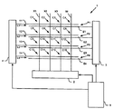
表示パネルの1以上の列又は行を選択するためのドライバ。
その第一の端部B1が該ドライバにより選択された該列又は行に接続されるソレノイド。
その負の端子が該ソレノイドLの第二の端部B2に接続され、その正の端子が第一のスイッチ素子を介して該ソレノイドの該第一の端部B1に接続され、該第一の直流電圧V1を生成することが意図される第一の直流電圧ジェネレータ。該第一のスイッチ素子Sは、該第一のフェーズの間は閉じた状態にあり、該第二、第三及び第四のフェーズの間は開いた状態にあり、該第五のフェーズの間は開いた状態又は閉じた状態にある。
その正の端子が該ソレノイドLの該第二の端部B2に接続されており、その負の端子が接地されており、該第二の直流電圧V2を生成することが意図される第二の直流電圧ジェネレータ。
そのカソードが該ソレノイドLの第一の端部B1に接続されており、そのアノードが接地されている第一のダイオード。
表示パネルの1以上の列又は行を選択するためのドライバ。
その第一の端部B1が該ドライバにより選択された該列又は行に接続されるソレノイド。
該第一の直流電圧V1を生成することが意図され、その正の端子が第一のスイッチ素子Sを介して該ソレノイドの該第一の端部B1に接続されており、その負の端子が第二のスイッチ素子S’を介して該ソレノイドの第二の端部B2に接続される第一の直流電圧ジェネレータ。該第一のスイッチ素子Sは、該第一及び第六のフェーズの間は閉じた状態にあり、該第二、第三、第四及び第五のフェーズの間は開いた状態にある。
その正の端子が該第一の直流電圧ジェネレータG1の負の端子に接続されており、その負の端子が接地されており、該第二の直流電圧V2を生成することが意図される第二の直流電圧ジェネレータ。
そのカソードが該ソレノイドの該第一の端部B1に接続されており、そのアノードが接地されている第一のダイオード。
固定された期間T1の第一のフェーズは、図5Aにより例示されており、この第一のフェーズの間、ソレノイドLは、磁気エネルギーの形式で電流を蓄積し、ドライバDにより選択されたPDPの列の端子に振幅Aの電圧が印加される。列ドライバのスイッチは、前の信号周期の間に書き込まれたデータに従って開閉の状態が決定される。
期間T2の第二のフェーズは、図5Bにより例示されており、この第二のフェーズの間、ソレノイドLに蓄積された電流の少なくとも1部は、列ドライバにより選択されたPDPの列に、これらの列の端子間の電圧がゼロになるまで放電される。
期間T5の第五のフェーズは、図5Eにより例示されており、この第五のフェーズの間、ドライバDにより選択された列の端子間の電圧は、書き込み電流が書込みされるべきセルを流れるように、振幅Aに保持される。
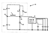
図5Aを参照して、期間T1のフェーズの間、スイッチ素子Sは閉じた状態にされる。電圧源G1、スイッチ素子S及びソレノイドLにより形成された回路を通して電流ILが流れる。電流ILの強度は、ソレノイドLに蓄積されている電流に合わせて増加する。この方法を例示するために採用される取り決めを使用して、電流ILは、この周期の間は正である。このフェーズの間、ドライバDのスイッチの状態は、前の信号周期の間に書き込まれたデータに依存する。ドライバDにより選択された列に対応するキャパシタの端子に印加される電圧は、A=V1+V2に等しい。

P=T1+T2+T3+T4+T5=1μs,
T1+T5=4(T2+T3+T4),
C=6nF(ドライバDにより制御される列のキャパシタンス。たとえば、PDPの列の27分の1に対応する。),
A=V1+V2=100V.
以下の値が得られる。L≒1μH,V1=20V及びV2=80V。
G1,G2:電圧源
S,S’ :スイッチ素子
D1〜D3:ダイオード
D :PDP列ドライバ
Claims (4)
- ドライバ、スイッチ素子、ソレノイド、第一の直流電圧発生器、第二の直流電圧発生器及びダイオードを備える装置において、複数の行及び列、並びに前記列と行の交点に配置されるセルを有する表示パネルの1以上の行又は列をアドレス指定するアドレス信号を発生する方法であって、
前記ドライバは、前記表示パネルの前記1以上の行又は列を選択し、
前記ソレノイドの第一の端部は、前記ドライバにより選択された行又は列と前記スイッチ素子の一方の端部に接続され、
前記第一の直流電圧発生器の負の端子は、前記ソレノイドの第二の端部に接続され、前記第一の直流電圧発生器の正の端子は、前記スイッチ素子の他方の端部を介して前記ソレノイドの前記第一の端部に接続され、前記第一の直流電圧発生器は、振幅V1を有する第一の直流電圧を発生し、
前記第二の直流電圧発生器の正の端子は、前記ソレノイドの前記第二の端部に接続され、前記第二の直流電圧発生器の負の端子は、接地され、前記第二の直流電圧発生器は、振幅V2を有する第二の直流電圧を発生し、
前記ダイオードのカソードは、前記ソレノイドの前記第一の端部に接続され、前記ダイオードのアノードは、接地され、
前記アドレス信号は、振幅(A=V1+V2)の電圧パルスを含み、前記ドライバにより前記表示パネルの1以上の行又は列に選択的に印加され、
前記スイッチ素子が閉じた状態にある期間T1の第一のフェーズの間、前記ソレノイドが、前記第一の直流電圧発生器、前記スイッチ素子及び前記ソレノイドにより形成される第一のループにおいて前記第一の端部から前記第二の端部への第一の方向で流れる電流によるエネルギーを蓄積するように、前記ソレノイドの端子間に前記第一の直流電圧を印加し、前記ドライバにより選択された列又は行の端子間に前記振幅Aの電圧を印加するステップと、
前記スイッチ素子が開いた状態にある期間T2の第二のフェーズの間、前記ソレノイド、前記第二の直流電圧発生器及び前記ドライバにより選択された前記列及び行により形成される第二のループにおいて前記第一の方向で、前記ドライバにより選択された前記列又は行に、前記列又は行の端子間の電圧がゼロになるまで前記ソレノイドに蓄積されたエネルギーの少なくとも一部を放電するステップと、
前記スイッチ素子が開いた状態にある期間T3の第三のフェーズの間、前記ドライバにより選択された前記列又は行の端子間でゼロ電圧を保持し、前記列又は行の選択を変更し、前記ソレノイド、前記第二の直流電圧発生器及び前記ダイオードにより形成される第三のループにおいて前記第一の方向で、前記ソレノイドに残されている電流を前記第二の直流電圧発生器により吸収するステップと、
前記スイッチ素子が開いた状態にある期間T4の第四のフェーズの間、前記列又は行の端子間の電圧が振幅Aに到達するまで、前記第二の直流電圧発生器、前記ソレノイド及び前記ドライバにより選択された前記列又は行により形成される第四のループにおいて、前記第二の直流電圧発生器により供給されるエネルギーで前記第一の方向とは反対の第二の方向で前記ソレノイドを充電するステップと、
前記スイッチ素子が閉じた状態にあるか又は開いた状態にある期間T5の第五のフェーズの間、前記第二の直流電圧発生器、前記ソレノイド及び前記ドライバにより選択された前記列又は行により形成されるループと、前記第一の直流電圧発生器、前記ソレノイド及び前記スイッチ素子により形成される第五のループとのそれぞれにおいて、前記第二の方向で前記ソレノイドを通して電流が流れることで、前記表示パネルのセルに書き込み電流を生じるように、前記ドライバにより選択された前記列又は行の間に形成された前記キャパシタの端子間で前記振幅Aの電圧を保持するステップと、
を備えることを特徴とする方法。 - 前記装置は、別のスイッチ素子を備え、
前記別のスイッチ素子の一方の端部は、前記ソレノイドの前記第二の端部に直列に接続され、前記別のスイッチ素子の他方の端部は、前記第一の直流電圧発生器の前記負の端子と前記第二の直流電圧発生器の前記正の端子とにそれぞれ接続され、前記別のスイッチ素子は、前記第一のフェーズから第五のフェーズにおいて閉じた状態にあり、
前記第五のフェーズの後、前記ドライバにより選択された前記列又は行に電流が流れない休止フェーズに対応する期間T6の第六のフェーズの間、前記別のスイッチ素子を開いた状態にし、前記列又は行の端子間の電圧を前記振幅Aに保持する、
ことを特徴とする請求項1記載の方法。 - 複数の行及び列、並びに前記列と行の交点に配置されるセルを有する表示パネルの1以上の行又は列をアドレス指定するアドレス信号を発生する装置であって、
表示パネルの1以上の列又は行を選択するドライバと、
スイッチ素子と、
その第一の端部が前記ドライバにより選択された前記列又は行及び前記スイッチ素子の一方の端部に接続されるソレノイドと、
その負の端子が前記ソレノイドの第二の端部に接続され、その正の端子が前記スイッチ素子の他方の端部を介して前記ソレノイドの前記第一の端部に接続され、V1の振幅を有する前記第一の直流電圧を生成する第一の直流電圧ジェネレータと、
その正の端子が前記ソレノイドの前記第二の端部に接続されており、その負の端子が接地されており、V2の振幅を有する前記第二の直流電圧を生成する第二の直流電圧ジェネレータと、
そのカソードが前記ソレノイドの第一の端部に接続されており、そのアノードが接地されている第一のダイオードとを備え、
前記アドレス信号は、振幅(A=V1+V2)の電圧パルスを含み、前記ドライバにより前記表示パネルの1以上の行又は列に選択的に印加され、
前記スイッチ素子が閉じた状態にある期間T1の第一のフェーズの間、前記ソレノイドが、前記第一の直流電圧発生器、前記スイッチ素子及び前記ソレノイドにより形成されるループにおいて前記第一の端部から前記第二の端部への第一の方向で流れる電流によるエネルギーを蓄積するように、前記ソレノイドの端子間に前記第一の直流電圧が印加され、前記ドライバにより選択された列又は行の端子間に前記振幅Aの電圧が印加され、
前記スイッチ素子が開いた状態にある期間T2の第二のフェーズの間、前記ソレノイド、前記第二の直流電圧発生器及び前記ドライバにより選択された前記列及び行により形成されるループにおいて前記第一の方向で、前記ドライバにより選択された前記列又は行に、前記列又は行の端子間の電圧がゼロになるまで前記ソレノイドに蓄積されたエネルギーの少なくとも一部が放電され、
前記スイッチ素子が開いた状態にある期間T3の第三のフェーズの間、前記ドライバにより選択された前記列又は行の端子間でゼロ電圧が保持され、前記列又は行の選択が変更され、前記ソレノイド、前記第二の直流電圧発生器及び前記ダイオードにより形成されるループにおいて前記第一の方向で、前記ソレノイドに残されている電流が前記第二の直流電圧発生器により吸収され、
前記スイッチ素子が開いた状態にある期間T4の第四のフェーズの間、前記列又は行の端子間の電圧が前記振幅Aに到達するまで、前記第二の直流電圧発生器、前記ソレノイド及び前記ドライバにより選択された前記列又は行により形成されるループにおいて、前記第二の直流電圧発生器により供給されるエネルギーで前記第一の方向とは反対の第二の方向で前記ソレノイドが充電され、
前記スイッチ素子が閉じた状態にあるか又は開いた状態にある期間T5の第五のフェーズの間、前記第二の直流電圧発生器、前記ソレノイド及び前記ドライバにより選択された前記列又は行により形成されるループと、前記第一の直流電圧発生器、前記ソレノイド及び前記スイッチ素子により形成されるループとのそれぞれにおいて、前記第二の方向で前記ソレノイドを通して電流が流れることで、前記表示パネルのセルに書き込み電流を生じるように、前記ドライバにより選択された前記列又は行の間に形成された前記キャパシタの端子間で前記振幅Aの電圧が保持される、
ことを特徴とする装置。 - 当該装置は、別のスイッチ素子を備え、
前記別のスイッチ素子の一方の端部は、前記ソレノイドの前記第二の端部に直列に接続され、前記別のスイッチ素子の他方の端部は、前記第一の直流電圧発生器の前記負の端子と前記第二の直流電圧発生器の前記正の端子とにそれぞれ接続され、前記別のスイッチ素子は、前記第一のフェーズから第五のフェーズにおいて閉じた状態にあり、
前記第五のフェーズの後、前記ドライバにより選択された前記列又は行に電流が流れない休止フェーズに対応する期間T6の第六のフェーズの間、前記別のスイッチ素子は開いた状態にされ、前記列又は行の端子間の電圧が前記振幅Aに保持される、
ことを特徴とする請求項3記載の装置。
Applications Claiming Priority (2)
| Application Number | Priority Date | Filing Date | Title |
|---|---|---|---|
| FR0309418 | 2003-07-31 | ||
| FR0309418A FR2858454A1 (fr) | 2003-07-31 | 2003-07-31 | Procede de generation d'un signal d'adressage dans un panneau plasma et dispositif mettant en oeuvre ledit procede |
Publications (3)
| Publication Number | Publication Date |
|---|---|
| JP2005070762A JP2005070762A (ja) | 2005-03-17 |
| JP2005070762A5 JP2005070762A5 (ja) | 2008-04-24 |
| JP4845355B2 true JP4845355B2 (ja) | 2011-12-28 |
Family
ID=33523026
Family Applications (1)
| Application Number | Title | Priority Date | Filing Date |
|---|---|---|---|
| JP2004223476A Expired - Fee Related JP4845355B2 (ja) | 2003-07-31 | 2004-07-30 | プラズマパネルにおいてアドレス信号を発生する方法、及び該方法を実現するための装置 |
Country Status (7)
| Country | Link |
|---|---|
| US (1) | US7408542B2 (ja) |
| EP (1) | EP1503361A3 (ja) |
| JP (1) | JP4845355B2 (ja) |
| KR (1) | KR20050014691A (ja) |
| CN (1) | CN100409288C (ja) |
| FR (1) | FR2858454A1 (ja) |
| TW (1) | TW200504659A (ja) |
Families Citing this family (3)
| Publication number | Priority date | Publication date | Assignee | Title |
|---|---|---|---|---|
| FR2876210A1 (fr) * | 2004-10-01 | 2006-04-07 | Thomson Licensing Sa | Dispositif de generation de signaux d'entretien sur les colonnes d'un panneau plasma et panneau plasma comprenant ce dispositif |
| KR20060089934A (ko) * | 2005-02-03 | 2006-08-10 | 삼성전자주식회사 | 트랜지스터 수가 감소된 전류 구동 데이터 드라이버 |
| US20110169811A1 (en) * | 2008-04-22 | 2011-07-14 | Panasonic Corporation | Plasma display apparatus and method of driving plasma display panel |
Family Cites Families (15)
| Publication number | Priority date | Publication date | Assignee | Title |
|---|---|---|---|---|
| US4866349A (en) * | 1986-09-25 | 1989-09-12 | The Board Of Trustees Of The University Of Illinois | Power efficient sustain drivers and address drivers for plasma panel |
| JP2735014B2 (ja) * | 1994-12-07 | 1998-04-02 | 日本電気株式会社 | 表示パネルの駆動回路 |
| DE19737662A1 (de) * | 1997-08-29 | 1999-03-04 | Thomson Brandt Gmbh | Wechselspannungsgenerator zur Steuerung eines Plasma-Wiedergabeschirms |
| JP3568098B2 (ja) * | 1998-06-03 | 2004-09-22 | パイオニア株式会社 | 表示パネルの駆動装置 |
| US7053869B2 (en) * | 2000-02-24 | 2006-05-30 | Lg Electronics Inc. | PDP energy recovery apparatus and method and high speed addressing method using the same |
| US6366063B1 (en) * | 2000-03-22 | 2002-04-02 | Nec Corporation | Circuit and method for driving capacitive load |
| JP2001337640A (ja) * | 2000-03-22 | 2001-12-07 | Nec Corp | 容量性負荷の駆動回路及び駆動方法 |
| TW555122U (en) * | 2000-08-22 | 2003-09-21 | Koninkl Philips Electronics Nv | Matrix display driver with energy recovery |
| CN1272758C (zh) * | 2000-11-09 | 2006-08-30 | Lg电子株式会社 | 能够提升电压的能量回收电路及其提高能效的方法 |
| TW540026B (en) * | 2001-12-28 | 2003-07-01 | Au Optronics Corp | Method for driving a plasma display panel |
| DE10200827A1 (de) * | 2002-01-11 | 2003-07-24 | Philips Intellectual Property | Verfahren zum Steuern einer Schaltungsanordnung für die Wechselspannungsversorgung eines Plasma-Display-Panels |
| KR100482348B1 (ko) * | 2003-04-16 | 2005-04-14 | 엘지전자 주식회사 | 플라즈마 디스플레이 패널의 에너지 회수장치 및 회수방법 |
| JP4846974B2 (ja) * | 2003-06-18 | 2011-12-28 | 株式会社日立製作所 | プラズマディスプレイ装置 |
| FR2857145A1 (fr) * | 2003-07-02 | 2005-01-07 | Thomson Plasma | Procede de generation d'impulsions breves sur une pluralite de colonnes ou lignes d'un panneau plasma et dispositif pour mettre en oeuvre ledit procede |
| KR100508255B1 (ko) * | 2003-07-15 | 2005-08-18 | 엘지전자 주식회사 | 에너지 회수회로 및 그 구동방법 |
-
2003
- 2003-07-31 FR FR0309418A patent/FR2858454A1/fr active Pending
-
2004
- 2004-07-13 EP EP04077026A patent/EP1503361A3/en not_active Withdrawn
- 2004-07-20 CN CNB2004100713522A patent/CN100409288C/zh not_active Expired - Fee Related
- 2004-07-28 KR KR1020040059182A patent/KR20050014691A/ko not_active Application Discontinuation
- 2004-07-30 TW TW093122809A patent/TW200504659A/zh unknown
- 2004-07-30 JP JP2004223476A patent/JP4845355B2/ja not_active Expired - Fee Related
- 2004-08-02 US US10/909,913 patent/US7408542B2/en active Active
Also Published As
| Publication number | Publication date |
|---|---|
| KR20050014691A (ko) | 2005-02-07 |
| JP2005070762A (ja) | 2005-03-17 |
| CN100409288C (zh) | 2008-08-06 |
| US7408542B2 (en) | 2008-08-05 |
| TW200504659A (en) | 2005-02-01 |
| EP1503361A3 (en) | 2008-04-30 |
| EP1503361A2 (en) | 2005-02-02 |
| CN1581271A (zh) | 2005-02-16 |
| FR2858454A1 (fr) | 2005-02-04 |
| US20050068260A1 (en) | 2005-03-31 |
Similar Documents
| Publication | Publication Date | Title |
|---|---|---|
| US7483000B2 (en) | Apparatus and method for driving a plasma display panel | |
| KR100490614B1 (ko) | 플라즈마 디스플레이 패널의 구동 장치 및 그 구동 방법 | |
| KR100578854B1 (ko) | 플라즈마 표시 장치와 그 구동 방법 | |
| JP2006079088A (ja) | プラズマディスプレイ装置及びその駆動方法 | |
| KR100502905B1 (ko) | 플라즈마 디스플레이 패널의 구동 장치 및 구동 방법 | |
| JP4845355B2 (ja) | プラズマパネルにおいてアドレス信号を発生する方法、及び該方法を実現するための装置 | |
| KR100467450B1 (ko) | 플라즈마 디스플레이 패널과 그 구동 장치 및 구동 방법 | |
| KR100589882B1 (ko) | 디스플레이 패널 구동 방법 | |
| US7479936B2 (en) | Plasma display and its driving method and circuit | |
| JP2005025153A (ja) | 容量性発光素子の駆動装置 | |
| EP1780691A1 (en) | Driving apparatus and method for a plasma display panel | |
| JP4866540B2 (ja) | プラズマ・ディスプレイの複数の列又は行に短持続時間パルスを生成する方法及び該方法を実施するデバイス | |
| KR101071304B1 (ko) | 플라즈마 디스플레이 패널을 구동하기 위한 디바이스 | |
| KR100502906B1 (ko) | 플라즈마 디스플레이 패널의 구동 방법 | |
| KR100458574B1 (ko) | 플라즈마 디스플레이 패널의 구동 장치 및 방법 | |
| KR100786876B1 (ko) | 플라즈마 표시 장치 및 그 구동 방법 | |
| JP2004274827A (ja) | 電源装置および表示パネル駆動装置 | |
| KR100649526B1 (ko) | 플라즈마 표시 장치 및 그 구동 방법 | |
| KR100649193B1 (ko) | 플라즈마 표시 장치 및 그의 구동 방법 | |
| KR20030088634A (ko) | 플라즈마 디스플레이 패널의 구동 방법 | |
| KR100649191B1 (ko) | 플라즈마 표시 장치 및 그 구동 방법 | |
| KR20090119199A (ko) | 플라즈마 표시 장치 및 그 구동 방법 | |
| JP2008077049A (ja) | プラズマ表示装置、プラズマ表示装置の駆動装置およびプラズマ表示装置の駆動方法 | |
| JP2005031615A (ja) | 表示装置およびその駆動方法 | |
| KR20060042844A (ko) | 낮은 리셋전압으로 구동되는 플라즈마 디스플레이 패널의구동 장치 |
Legal Events
| Date | Code | Title | Description |
|---|---|---|---|
| A621 | Written request for application examination |
Free format text: JAPANESE INTERMEDIATE CODE: A621 Effective date: 20070719 |
|
| A521 | Written amendment |
Free format text: JAPANESE INTERMEDIATE CODE: A523 Effective date: 20080311 |
|
| A977 | Report on retrieval |
Free format text: JAPANESE INTERMEDIATE CODE: A971007 Effective date: 20100616 |
|
| A131 | Notification of reasons for refusal |
Free format text: JAPANESE INTERMEDIATE CODE: A131 Effective date: 20100706 |
|
| A521 | Written amendment |
Free format text: JAPANESE INTERMEDIATE CODE: A523 Effective date: 20101001 |
|
| A131 | Notification of reasons for refusal |
Free format text: JAPANESE INTERMEDIATE CODE: A131 Effective date: 20110111 |
|
| TRDD | Decision of grant or rejection written | ||
| A01 | Written decision to grant a patent or to grant a registration (utility model) |
Free format text: JAPANESE INTERMEDIATE CODE: A01 Effective date: 20110920 |
|
| A01 | Written decision to grant a patent or to grant a registration (utility model) |
Free format text: JAPANESE INTERMEDIATE CODE: A01 |
|
| A61 | First payment of annual fees (during grant procedure) |
Free format text: JAPANESE INTERMEDIATE CODE: A61 Effective date: 20111011 |
|
| FPAY | Renewal fee payment (event date is renewal date of database) |
Free format text: PAYMENT UNTIL: 20141021 Year of fee payment: 3 |
|
| R150 | Certificate of patent or registration of utility model |
Free format text: JAPANESE INTERMEDIATE CODE: R150 |
|
| LAPS | Cancellation because of no payment of annual fees |