JP4841981B2 - Manufacturing method of light receiving module - Google Patents
Manufacturing method of light receiving module Download PDFInfo
- Publication number
- JP4841981B2 JP4841981B2 JP2006076596A JP2006076596A JP4841981B2 JP 4841981 B2 JP4841981 B2 JP 4841981B2 JP 2006076596 A JP2006076596 A JP 2006076596A JP 2006076596 A JP2006076596 A JP 2006076596A JP 4841981 B2 JP4841981 B2 JP 4841981B2
- Authority
- JP
- Japan
- Prior art keywords
- light receiving
- manufacturing
- resin molded
- resin
- molded body
- Prior art date
- Legal status (The legal status is an assumption and is not a legal conclusion. Google has not performed a legal analysis and makes no representation as to the accuracy of the status listed.)
- Expired - Fee Related
Links
Images


Classifications
-
- H—ELECTRICITY
- H10—SEMICONDUCTOR DEVICES; ELECTRIC SOLID-STATE DEVICES NOT OTHERWISE PROVIDED FOR
- H10W—GENERIC PACKAGES, INTERCONNECTIONS, CONNECTORS OR OTHER CONSTRUCTIONAL DETAILS OF DEVICES COVERED BY CLASS H10
- H10W74/00—Encapsulations, e.g. protective coatings
- H10W74/10—Encapsulations, e.g. protective coatings characterised by their shape or disposition
Landscapes
- Light Receiving Elements (AREA)
Description
本発明は、たとえば家庭用電化製品のリモコン送信機から送信された赤外線の受信に用いられる受光モジュールの製造方法に関する。 The present invention relates to a method of manufacturing a light receiving module used for receiving infrared rays transmitted from, for example, a remote control transmitter of a household appliance.
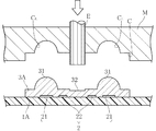
リモコン受信用の受光モジュールの一つとして、基板に受光素子が搭載された面実装型の受光モジュールが知られている(たとえば、特許文献1参照)。図12は、そのような受モジュールの一例を示している。同図に示された受光モジュールXは、基板91に受光素子92と駆動IC93とが搭載されている。基板91上には、受光素子92および駆動IC93を封止する樹脂パッケージ95が設けられている。樹脂パッケージ95には、受光素子92の正面に位置するレンズ95aが形成されている。受光モジュールXに向かってきた赤外線は、レンズ95aによって受光素子92に集光される。受光モジュールXは、受光素子92が受光した赤外線に応じた信号を図外の端子から出力可能に構成されている。
As one of the light receiving modules for remote control reception, a surface mount type light receiving module in which a light receiving element is mounted on a substrate is known (for example, see Patent Document 1). FIG. 12 shows an example of such a receiving module. In the light receiving module X shown in the figure, a
受光モジュールXの製造工程においては、複数の受光モジュールXの製造を一括して行うことが一般的である(たとえば、特許文献2参照)。図13は、受光モジュールXの製造方法の一例における一過程を示している。集合基板91Aは、基板91を複数個取り可能なサイズとされたものである。この集合基板91A上に複数の受光素子92および複数の駆動IC93を搭載する。集合基板91Aには、複数の樹脂成形体形成予定領域95Aが設定されている。各樹脂成形体形成予定領域95Aに、複数の受光素子92と複数の駆動IC93とを交互に直列配置する。樹脂成形体形成予定領域95Aに配置された複数の受光素子92および複数の駆動IC93を覆うように樹脂成形体を形成する。この樹脂成形体には、複数の受光素子92の正面に位置するレンズを形成しておく。この樹脂成形体の形成は、たとえば金型を用いて行う。そして受光素子92および駆動IC93が一つずつ含まれるように上記樹脂成形体と集合基板91Aとを切断する。これにより、複数の受光モジュールXが得られる。
In the manufacturing process of the light receiving module X, it is common to manufacture a plurality of light receiving modules X at once (for example, refer to Patent Document 2). FIG. 13 shows a process in an example of a method for manufacturing the light receiving module X. The
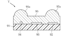
しかしながら、一般的に受光モジュールXを製造するメーカーは、受光モジュールX以外にもたとえば赤外線を用いた光通信モジュールを製造する場合が多い。図14は、そのような光通信モジュールの一例を示している。同図に示された光通信モジュールYは、受光素子92および駆動IC93に加えて発光素子94を備えている。樹脂パッケージ95には、受光素子92および発光素子94の正面に位置する2つのレンズ95aが形成されている。光通信モジュールYは、赤外線の送受信を行うことにより双方向の通信を可能に構成されている。このような光通信モジュールYを図13に示した集合基板91Aを用いて複数個製造しようとしても、受光モジュール92を製造するときとは、異なる金型を用いる必要がある。このため、製品の種類ごとに専用の金型を用意するためのコストが必要であった。また、製造する製品の種類を変更するたびに、上記金型の段取り替えを強いられていた。
However, in general, a manufacturer that manufactures the light receiving module X often manufactures an optical communication module using, for example, infrared rays in addition to the light receiving module X. FIG. 14 shows an example of such an optical communication module. The optical communication module Y shown in the figure includes a
本発明は、上記した事情のもとで考え出されたものであって、製品の作り分けを容易とすることが可能な受光モジュールの製造方法を提供することをその課題とする。 The present invention has been conceived under the circumstances described above, and it is an object of the present invention to provide a method for manufacturing a light receiving module capable of easily making a product.
本発明によって提供される受光モジュールの製造方法は、それぞれが受光素子および駆動ICを含む複数の素子群を集合基板に搭載する工程と、上記複数の素子群を覆う複数の樹脂成形体を形成する工程と、上記複数の樹脂成形体および上記集合基板を切断する工程と、を有する受光モジュールの製造方法であって、上記複数の素子群のうち同一の上記樹脂成形体に覆われる2つの上記素子群は、これらに含まれる2つの上記受光素子および2つの上記駆動ICが第1の方向において直列配置されており、かつ、2つの上記駆動ICどうしが隣り合う配置とされており、上記樹脂成形体には、上記各受光素子の正面に位置する複数のレンズが形成されていることを特徴としている。 The method for manufacturing a light receiving module provided by the present invention includes a step of mounting a plurality of element groups each including a light receiving element and a driving IC on a collective substrate, and forming a plurality of resin moldings covering the plurality of element groups. And a step of cutting the plurality of resin molded bodies and the collective substrate, wherein the two light receiving modules are covered with the same resin molded body among the plurality of element groups. In the group, the two light receiving elements included therein and the two drive ICs are arranged in series in the first direction, and the two drive ICs are adjacent to each other. The body is formed with a plurality of lenses positioned in front of the light receiving elements.
このような構成によれば、複数の上記受光モジュールを効率よく製造することができる。また、上記樹脂成形体には、上記2つの駆動ICを挟んで離間配置された少なくとも2つのレンズが形成されることとなる。このような2つのレンズを有する上記樹脂成形体は、たとえばこれらのレンズを上記受光素子と発光素子との正面に配置することにより、双方向通信が可能とされた光通信モジュールを製造することにも適している。このため、上記樹脂成形体を金型によって形成する場合、この金型を上記光通信モジュールの製造に流用することが可能である。したがって、種類の異なる製品を容易に作り分けることができる。 According to such a configuration, the plurality of light receiving modules can be efficiently manufactured. The resin molded body is formed with at least two lenses spaced apart from each other with the two drive ICs interposed therebetween. The resin molded body having such two lenses is, for example, for manufacturing an optical communication module capable of bidirectional communication by arranging these lenses in front of the light receiving element and the light emitting element. Is also suitable. For this reason, when the said resin molding is formed with a metal mold | die, it is possible to divert this metal mold | die for manufacture of the said optical communication module. Therefore, it is possible to easily make different types of products.
本発明の好ましい実施の形態においては、上記各樹脂成形体は、4つの上記素子群を覆っており、これら4つの素子群は、上記第1の方向において隣り合う2つの上記素子群の組が、上記第1の方向と直角である第2の方向において2組離間配置されている。このような構成によれば、上記樹脂成形体を4分割することにより、4つの上記受光モジュールを製造することが可能である。これに加えて、上記樹脂成形体によって発光素子を含む別の素子群を2つ覆う製造方法によれば、2つの光通信モジュールを容易に製造することができる。 In a preferred embodiment of the present invention, each of the resin molded bodies covers the four element groups, and the four element groups are formed by a set of two element groups adjacent in the first direction. In the second direction perpendicular to the first direction, two sets are spaced apart. According to such a configuration, it is possible to manufacture the four light receiving modules by dividing the resin molded body into four parts. In addition, according to the manufacturing method in which two other element groups including light emitting elements are covered with the resin molded body, two optical communication modules can be easily manufactured.
本発明のその他の特徴および利点は、添付図面を参照して以下に行う詳細な説明によって、より明らかとなろう。 Other features and advantages of the present invention will become more apparent from the detailed description given below with reference to the accompanying drawings.
以下、本発明の好ましい実施の形態につき、図面を参照して具体的に説明する。 Hereinafter, preferred embodiments of the present invention will be specifically described with reference to the drawings.
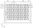
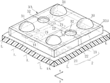
図1〜図7は、本発明に係る受光モジュールの製造方法の一例を示している。これらの図に示された製造方法においては、まず、図1に示すように、集合基板1Aを用意する。集合基板1Aは、ガラスエポキシなどの樹脂からなるプレートである。次に、集合基板1Aに複数の素子群2を搭載する。集合基板1Aには、本発明でいう第1の方向である方向xに4行、本発明でいう第2の方向である方向yに6列の配置とされた、計24個の樹脂成形体形成予定領域3A’が設定されている。各樹脂成形体形成予定領域3A’内には、4つの素子群2が配置されている。素子群2は、受光素子21および駆動IC22からなる。各素子群2の搭載においては、方向xに沿って受光素子21および駆動IC22を直列配置する。方向xにおいて隣り合う2つの素子群2は、互いの駆動IC22が隣接する配置とされている。方向yにおいて隣り合う2つの素子群2どうしは、受光素子22および駆動IC23の配置が同じとされている。素子群2の搭載は、たとえば集合基板1A上に形成された配線パターン(図示略)のパッド(図示略)に対してダイボンディングにより行う。
1 to 7 show an example of a method for manufacturing a light receiving module according to the present invention. In the manufacturing method shown in these drawings, first, as shown in FIG. 1, a
集合基板1Aには、素子群2に隣接する複数のスルーホール11を形成しておく。各素子群2には、3つずつのスルーホール11が隣接している。複数のスルーホール11は、方向xにおいて3つおきにいわゆる千鳥状に配置されている。図2に示すように、スルーホール11は、金属膜12に覆われている。金属膜12は、上述した配線パターンの適所に導通している。
A plurality of through
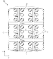
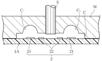
次いで、樹脂成形体形成予定領域3A’に図7に示す樹脂成形体3Aを形成する。樹脂成形体3Aの形成は、トランスファモールド法により行う。図3は、このトランスファモールド法に用いる金型Mを示している。本図は、金型Mをその開口側から見た図である。金型Mには、複数のキャビティCがマトリクス状に設けられている。キャビティCは、略直方体形状の凹部であり、図7に示す樹脂成形体3Aを形作る部分である。図3に示すように、キャビティCには、4つのドーム状の凹部CLが形成されている。凹部CLは、図7に示すレンズ31を形作る部分である。また、金型Mには、キャビティC毎に2つずつエジェクタピンEが設けられている。各エジェクタピンEは、2つの凹部CLの間に位置している。
Next, a resin molded
樹脂成形体3Aを形成するには、図4に示すように、金型Mを集合基板1に押し当てる。図4は、図3に示すIV−IV線に沿った金型Mおよび集合基板1Aの断面を示したものである。各キャビティC内には4つずつの素子群2を収容する。この状態で、キャビティC内に樹脂材料を注入する。この樹脂材料を硬化させると、図5に示す樹脂成形体3Aが得られる。樹脂成形体3Aには、キャビティCに形成された凹部CLにより、レンズ31が形成される。
In order to form the resin molded
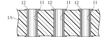
上記樹脂材料が硬化した後は、エジェクタピンEを図中下方に前進させることにより、金型Mから、樹脂成形体3Aを取り外す。これにより、図6に示すように集合基板1A上に複数の樹脂成形体3Aを形成できる。図7に示すように、樹脂成形体3Aには、4つのレンズ31が形成される。2つのレンズ31間には、エジェクタピン痕32が形成されている。
After the resin material is cured, the resin molded
この後は、集合基板1Aおよび樹脂成形体3Aを切断する。この切断は、図7に表された切断線Lに沿って行う。方向xに延びる切断線Lは、複数のスルーホール11と重なっている。この切断線Lに沿って切断することにより、スルーホール11は、断面半円形状に分割される。方向xおよび方向yに延びる全ての切断線Lに沿った切断が完了すると、各樹脂成形体3Aが分割されて4つの樹脂パッケージ3となり、集合基板1Aが分割されて複数の基板1となる。この結果、図8に示す受光モジュールA1が複数個得られる。
Thereafter, the
図8に示す受光モジュールAは、基板1、受光素子21、駆動IC22、および樹脂パッケージ3を備えている。
The light receiving module A shown in FIG. 8 includes a
基板1は、ガラスエポキシなどの樹脂により、全体として平面視長矩形状に形成されている。基板1には、配線パターン(図示略)が形成されている。
The board |
受光素子21は、たとえば、赤外線を感知することができるPINフォトダイオードなどからなり、ワイヤボンディング(図示略)により上記配線パターンと接続されている。受光素子21は、赤外線を受光すると、その光量に応じた出力信号を出力可能に構成されている。
The
駆動IC22は、受光素子21による受信動作を制御するためのものである。駆動IC22は、ワイヤボンディング(図示略)により上記配線パターンと接続され、かつ上記配線パターンを通じて受光素子21に接続されている。
The driving
樹脂パッケージ3は、たとえば顔料を含んだエポキシ樹脂により形成されており、可視光に対しては透光性を有しない反面、赤外線に対しては透光性を有する。この樹脂パッケージ3は、受光素子21および駆動IC22からなる素子群2を覆うように基板1上に設けられている。樹脂パッケージ3には、レンズ31が一体的に形成されている。レンズ31は、受光素子21の正面に位置しており、受光モジュールAに送信されてきた赤外線を集光して受光素子21に入射するように構成されている。樹脂パッケージ3には、上述したエジェクタピン痕32の一部分が、エジェクタピン痕32aとして残存している。基板1の側面には、分割されたスルーホール11を覆う金属膜12によって面実装用の端子が形成されている。
The
このように、本実施形態によれば、複数の受光モジュールAを適切に、かつ効率よく製造することが可能である。これに加えて、図3〜図5に示した金型Mは、受光モジュールAとは異なる、双方向通信が可能とされた光通信モジュールの製造にも用いることができる。 Thus, according to this embodiment, it is possible to manufacture a plurality of light receiving modules A appropriately and efficiently. In addition to this, the mold M shown in FIGS. 3 to 5 can be used for manufacturing an optical communication module different from the light receiving module A and capable of bidirectional communication.
図9は、集合基板1Aに光通信モジュールを構成するための素子群2を搭載した状態を示している。上記光通信モジュールを製造する場合、素子群2には、受光素子21、駆動IC22に加えて、発光素子23が含まれる。樹脂成形体形成予定領域3A’には、2つの素子群2が配置されている。集合基板1Aに複数の樹脂成形体形成予定領域3A’が設定される点は、上述した受光モジュールAの製造方法と同様である。
FIG. 9 shows a state in which the
次に、図3〜図5に示した金型Mを図9に示す集合基板1Aに押し付け、キャビティC内に樹脂材料を充填する。これにより、図10に示すように、樹脂成形体3Aを形成する。樹脂成形体3Aの4つのレンズ31は、それぞれ受光素子21および発光素子23の正面に位置することとなる。そして、樹脂成形体3Aおよび集合基板1Aを、素子群2どうしが分離されるように切断することにより、図11に示す光通信モジュールBを複数個製造することができる。光通信モジュールBは、発光素子23からレンズ31を通して指向性が高められた赤外線を出射可能とされている。駆動IC22は、発光素子23を用いた送信と受光素子21を用いた受信とを駆動制御可能とされている。
Next, the mold M shown in FIGS. 3 to 5 is pressed against the
金型MのキャビティCに設けられた4つの凹部CLが、2つの光通信モジュールBのレンズ31を形成するのに適した配置となっている。このため、光通信モジュールBの製造を受光モジュールAの製造とほとんど同じ手順で行うことができる。これは、受光モジュールAを製造する場合に、図1に示すように方向xに隣り合う2つの素子群2どうしを、それぞれの駆動IC22が隣接するように配置しているからである。
Four recesses C L provided in the cavity C of the mold M has a configuration suitable for forming the
また、金型のキャビティCは、4つの受光モジュールA、あるいは2つの光通信モジュールBに相当する部分を形成可能な形状およびサイズとされている。このため、受光モジュールAおよび光通信モジュールBの双方を効率よく製造することが可能となっている。 The cavity C of the mold has a shape and a size that can form portions corresponding to the four light receiving modules A or the two optical communication modules B. For this reason, it is possible to efficiently manufacture both the light receiving module A and the optical communication module B.
本発明に係る受光モジュールの製造方法は、上述した実施形態に限定されるものではない。本発明に係る受光モジュールの製造方法の各部の具体的な構成は、種々に設計変更自在である。 The method for manufacturing the light receiving module according to the present invention is not limited to the above-described embodiment. The specific configuration of each part of the manufacturing method of the light receiving module according to the present invention can be changed in various ways.
A 受光モジュール
B 光通信モジュール
x 第1の方向
y 第2の方向
1 基板
1A 集合基板
2 素子群
3 樹脂パッケージ
3A 樹脂成形体
3A’ 樹脂成形体形成予定領域
11 スルーホール
12 金属膜
21 受光素子
22 駆動IC
23 発光素子
31 レンズ
A Light-receiving module B Optical communication module x First direction y
23
Claims (2)
上記複数の素子群を覆う複数の樹脂成形体を形成する工程と、
上記複数の樹脂成形体および上記集合基板を切断する工程と、を有する受光モジュールの製造方法であって、
上記複数の素子群のうち同一の上記樹脂成形体に覆われる2つの上記素子群は、これらに含まれる2つの上記受光素子および2つの上記駆動ICが第1の方向において直列配置されており、かつ、2つの上記駆動ICどうしが隣り合う配置とされており、
上記樹脂成形体には、上記各受光素子の正面に位置する複数のレンズが形成されていることを特徴とする、受光モジュールの製造方法。 Mounting a plurality of element groups each including a light receiving element and a driving IC on a collective substrate;
Forming a plurality of resin moldings covering the plurality of element groups;
Cutting the plurality of resin molded bodies and the collective substrate, and a method of manufacturing a light receiving module,
In the two element groups covered by the same resin molded body among the plurality of element groups, the two light receiving elements included therein and the two drive ICs are arranged in series in the first direction, In addition, the two drive ICs are arranged next to each other,
A method for manufacturing a light receiving module, wherein the resin molding is formed with a plurality of lenses positioned in front of the light receiving elements.
これら4つの素子群は、上記第1の方向において隣り合う2つの上記素子群の組が、上記第1の方向と直角である第2の方向において2組離間配置されている、請求項1に記載の受光モジュールの製造方法。 Each of the resin moldings covers the four element groups,
The four element groups are arranged in such a manner that two sets of the two element groups adjacent in the first direction are separated from each other in a second direction perpendicular to the first direction. The manufacturing method of the light reception module of description.
Priority Applications (1)
| Application Number | Priority Date | Filing Date | Title |
|---|---|---|---|
| JP2006076596A JP4841981B2 (en) | 2006-03-20 | 2006-03-20 | Manufacturing method of light receiving module |
Applications Claiming Priority (1)
| Application Number | Priority Date | Filing Date | Title |
|---|---|---|---|
| JP2006076596A JP4841981B2 (en) | 2006-03-20 | 2006-03-20 | Manufacturing method of light receiving module |
Publications (2)
| Publication Number | Publication Date |
|---|---|
| JP2007258203A JP2007258203A (en) | 2007-10-04 |
| JP4841981B2 true JP4841981B2 (en) | 2011-12-21 |
Family
ID=38632175
Family Applications (1)
| Application Number | Title | Priority Date | Filing Date |
|---|---|---|---|
| JP2006076596A Expired - Fee Related JP4841981B2 (en) | 2006-03-20 | 2006-03-20 | Manufacturing method of light receiving module |
Country Status (1)
| Country | Link |
|---|---|
| JP (1) | JP4841981B2 (en) |
Families Citing this family (1)
| Publication number | Priority date | Publication date | Assignee | Title |
|---|---|---|---|---|
| KR102355524B1 (en) * | 2020-05-29 | 2022-01-24 | 주식회사 옵토웰 | Optical sensor module and manufacturing method of optical sensor module |
Family Cites Families (2)
| Publication number | Priority date | Publication date | Assignee | Title |
|---|---|---|---|---|
| JP4108162B2 (en) * | 1997-10-21 | 2008-06-25 | シチズン電子株式会社 | Infrared data communication module manufacturing method |
| JP4064579B2 (en) * | 1999-09-10 | 2008-03-19 | ローム株式会社 | Infrared data communication module manufacturing method |
-
2006
- 2006-03-20 JP JP2006076596A patent/JP4841981B2/en not_active Expired - Fee Related
Also Published As
| Publication number | Publication date |
|---|---|
| JP2007258203A (en) | 2007-10-04 |
Similar Documents
| Publication | Publication Date | Title |
|---|---|---|
| JP4878053B2 (en) | Manufacturing method of light emitting diode | |
| TWI715758B (en) | Semiconductor device package and a method of manufacturing the same | |
| US20040126117A1 (en) | Optical module and a method of fabricating the same | |
| TWI426621B (en) | Light emitting unit, apparatus and method for manufacturing the same, device for molding the same, and light emitting device package thereof | |
| US20060027479A1 (en) | Optical or electronic module and method for its production | |
| JP6442504B2 (en) | Conversion element and method of manufacturing optoelectronic component | |
| EP1976028A1 (en) | Method of photoelement resin sealing/molding | |
| US8110842B2 (en) | Light-emitting diode module and manufacturing method thereof | |
| CN106206915B (en) | A kind of integrated morphology and its manufacturing method of optical chip | |
| US6693304B2 (en) | Laminated lead frame, and optical communication module and method of manufacturing the same | |
| JP4841981B2 (en) | Manufacturing method of light receiving module | |
| JP2009042469A (en) | Optical module, optical module manufacturing method, optical / electronic composite circuit configured using the optical module, and manufacturing method thereof | |
| JP4811913B2 (en) | Manufacturing method of optical communication module | |
| JP5255950B2 (en) | Manufacturing method of optical semiconductor device | |
| JP4926421B2 (en) | Optical communication module and manufacturing method thereof | |
| JP2000353828A (en) | Photoelectric conversion element and method for manufacturing the same | |
| KR101171051B1 (en) | Printed circuit board having subborrd type optical printed circuit board module for high speed data transmission between high speed chips | |
| KR101430480B1 (en) | Wafer level lens unit and light emitting device package using the same | |
| JP3401128B2 (en) | Method for manufacturing multi-channel optical coupling device | |
| CN112447697A (en) | Electronic device comprising an optical electronic component and method of manufacturing | |
| US20050098710A1 (en) | Image sensor package | |
| US20260033373A1 (en) | Method for the mass production of electronic devices incorporating protection elements, and resulting electronic devices | |
| KR101364020B1 (en) | Semiconductor package and the fabriation method thereof | |
| JP3676348B2 (en) | Misaligned wire bonding image sensor | |
| JP2019211554A (en) | Mold for support member of optical receptacle body, support member and manufacturing method for the same, optical receptacle, and optical module |
Legal Events
| Date | Code | Title | Description |
|---|---|---|---|
| A621 | Written request for application examination |
Free format text: JAPANESE INTERMEDIATE CODE: A621 Effective date: 20080911 |
|
| A977 | Report on retrieval |
Free format text: JAPANESE INTERMEDIATE CODE: A971007 Effective date: 20101214 |
|
| TRDD | Decision of grant or rejection written | ||
| A01 | Written decision to grant a patent or to grant a registration (utility model) |
Free format text: JAPANESE INTERMEDIATE CODE: A01 Effective date: 20111004 |
|
| A01 | Written decision to grant a patent or to grant a registration (utility model) |
Free format text: JAPANESE INTERMEDIATE CODE: A01 |
|
| A61 | First payment of annual fees (during grant procedure) |
Free format text: JAPANESE INTERMEDIATE CODE: A61 Effective date: 20111005 |
|
| R150 | Certificate of patent or registration of utility model |
Free format text: JAPANESE INTERMEDIATE CODE: R150 |
|
| FPAY | Renewal fee payment (event date is renewal date of database) |
Free format text: PAYMENT UNTIL: 20141014 Year of fee payment: 3 |
|
| LAPS | Cancellation because of no payment of annual fees |