JP4841981B2 - 受光モジュールの製造方法 - Google Patents
受光モジュールの製造方法 Download PDFInfo
- Publication number
- JP4841981B2 JP4841981B2 JP2006076596A JP2006076596A JP4841981B2 JP 4841981 B2 JP4841981 B2 JP 4841981B2 JP 2006076596 A JP2006076596 A JP 2006076596A JP 2006076596 A JP2006076596 A JP 2006076596A JP 4841981 B2 JP4841981 B2 JP 4841981B2
- Authority
- JP
- Japan
- Prior art keywords
- light receiving
- manufacturing
- resin molded
- resin
- molded body
- Prior art date
- Legal status (The legal status is an assumption and is not a legal conclusion. Google has not performed a legal analysis and makes no representation as to the accuracy of the status listed.)
- Expired - Fee Related
Links
Images


Classifications
-
- H—ELECTRICITY
- H10—SEMICONDUCTOR DEVICES; ELECTRIC SOLID-STATE DEVICES NOT OTHERWISE PROVIDED FOR
- H10W—GENERIC PACKAGES, INTERCONNECTIONS, CONNECTORS OR OTHER CONSTRUCTIONAL DETAILS OF DEVICES COVERED BY CLASS H10
- H10W74/00—Encapsulations, e.g. protective coatings
- H10W74/10—Encapsulations, e.g. protective coatings characterised by their shape or disposition
Landscapes
- Light Receiving Elements (AREA)
Description
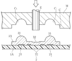
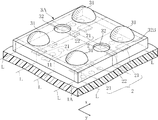
B 光通信モジュール
x 第1の方向
y 第2の方向
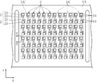
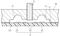
1 基板
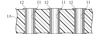
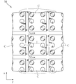
1A 集合基板
2 素子群
3 樹脂パッケージ
3A 樹脂成形体
3A’ 樹脂成形体形成予定領域
11 スルーホール
12 金属膜
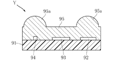
21 受光素子
22 駆動IC
23 発光素子
31 レンズ
Claims (2)
- それぞれが受光素子および駆動ICを含む複数の素子群を集合基板に搭載する工程と、
上記複数の素子群を覆う複数の樹脂成形体を形成する工程と、
上記複数の樹脂成形体および上記集合基板を切断する工程と、を有する受光モジュールの製造方法であって、
上記複数の素子群のうち同一の上記樹脂成形体に覆われる2つの上記素子群は、これらに含まれる2つの上記受光素子および2つの上記駆動ICが第1の方向において直列配置されており、かつ、2つの上記駆動ICどうしが隣り合う配置とされており、
上記樹脂成形体には、上記各受光素子の正面に位置する複数のレンズが形成されていることを特徴とする、受光モジュールの製造方法。 - 上記各樹脂成形体は、4つの上記素子群を覆っており、
これら4つの素子群は、上記第1の方向において隣り合う2つの上記素子群の組が、上記第1の方向と直角である第2の方向において2組離間配置されている、請求項1に記載の受光モジュールの製造方法。
Priority Applications (1)
| Application Number | Priority Date | Filing Date | Title |
|---|---|---|---|
| JP2006076596A JP4841981B2 (ja) | 2006-03-20 | 2006-03-20 | 受光モジュールの製造方法 |
Applications Claiming Priority (1)
| Application Number | Priority Date | Filing Date | Title |
|---|---|---|---|
| JP2006076596A JP4841981B2 (ja) | 2006-03-20 | 2006-03-20 | 受光モジュールの製造方法 |
Publications (2)
| Publication Number | Publication Date |
|---|---|
| JP2007258203A JP2007258203A (ja) | 2007-10-04 |
| JP4841981B2 true JP4841981B2 (ja) | 2011-12-21 |
Family
ID=38632175
Family Applications (1)
| Application Number | Title | Priority Date | Filing Date |
|---|---|---|---|
| JP2006076596A Expired - Fee Related JP4841981B2 (ja) | 2006-03-20 | 2006-03-20 | 受光モジュールの製造方法 |
Country Status (1)
| Country | Link |
|---|---|
| JP (1) | JP4841981B2 (ja) |
Families Citing this family (1)
| Publication number | Priority date | Publication date | Assignee | Title |
|---|---|---|---|---|
| KR102355524B1 (ko) * | 2020-05-29 | 2022-01-24 | 주식회사 옵토웰 | 광센서 모듈 및 광센서 모듈 제조방법 |
Family Cites Families (2)
| Publication number | Priority date | Publication date | Assignee | Title |
|---|---|---|---|---|
| JP4108162B2 (ja) * | 1997-10-21 | 2008-06-25 | シチズン電子株式会社 | 赤外線データ通信モジュールの製造方法 |
| JP4064579B2 (ja) * | 1999-09-10 | 2008-03-19 | ローム株式会社 | 赤外線データ通信モジュールの製造方法 |
-
2006
- 2006-03-20 JP JP2006076596A patent/JP4841981B2/ja not_active Expired - Fee Related
Also Published As
| Publication number | Publication date |
|---|---|
| JP2007258203A (ja) | 2007-10-04 |
Similar Documents
| Publication | Publication Date | Title |
|---|---|---|
| JP4878053B2 (ja) | 発光ダイオードの製造方法 | |
| TWI715758B (zh) | 半導體器件封裝件及製造其之方法 | |
| US20040126117A1 (en) | Optical module and a method of fabricating the same | |
| TWI426621B (zh) | 發光單元、用於製造此單元之裝置與方法、用於模製其透鏡之裝置、以及其發光裝置封裝 | |
| US20060027479A1 (en) | Optical or electronic module and method for its production | |
| JP6442504B2 (ja) | 変換要素およびオプトエレクトロニクス部品の製造方法 | |
| EP1976028A1 (en) | Method of photoelement resin sealing/molding | |
| US8110842B2 (en) | Light-emitting diode module and manufacturing method thereof | |
| CN106206915B (zh) | 一种光学芯片的集成结构及其制造方法 | |
| US6693304B2 (en) | Laminated lead frame, and optical communication module and method of manufacturing the same | |
| JP4841981B2 (ja) | 受光モジュールの製造方法 | |
| JP2009042469A (ja) | 光モジュール、光モジュールの製造方法、光モジュールを用いて構成された光・電子複合回路、およびその製造方法 | |
| JP4811913B2 (ja) | 光通信モジュールの製造方法 | |
| JP5255950B2 (ja) | 光半導体装置の製造方法 | |
| JP4926421B2 (ja) | 光通信モジュールおよびその製造方法 | |
| JP2000353828A (ja) | 光電変換素子およびその製造方法 | |
| KR101171051B1 (ko) | 고속칩들간의 고속 테이터 전송을 위한 서브 보드인 광 pcb 모듈을 구비한 인쇄회로기판 | |
| KR101430480B1 (ko) | 웨이퍼 레벨 렌즈부 및 이를 이용한 발광 소자 패키지 | |
| JP3401128B2 (ja) | 多チャンネル型光結合装置の製造方法 | |
| CN112447697A (zh) | 包括光学电子组件的电子设备以及制造方法 | |
| US20050098710A1 (en) | Image sensor package | |
| US20260033373A1 (en) | Method for the mass production of electronic devices incorporating protection elements, and resulting electronic devices | |
| KR101364020B1 (ko) | 반도체 패키지 및 그 제조 방법 | |
| JP3676348B2 (ja) | 位置ずれワイヤボンディング式イメージセンサ | |
| JP2019211554A (ja) | 光レセプタクル本体の支持部材用金型、支持部材及びその製造方法、光レセプタクル並びに光モジュール |
Legal Events
| Date | Code | Title | Description |
|---|---|---|---|
| A621 | Written request for application examination |
Free format text: JAPANESE INTERMEDIATE CODE: A621 Effective date: 20080911 |
|
| A977 | Report on retrieval |
Free format text: JAPANESE INTERMEDIATE CODE: A971007 Effective date: 20101214 |
|
| TRDD | Decision of grant or rejection written | ||
| A01 | Written decision to grant a patent or to grant a registration (utility model) |
Free format text: JAPANESE INTERMEDIATE CODE: A01 Effective date: 20111004 |
|
| A01 | Written decision to grant a patent or to grant a registration (utility model) |
Free format text: JAPANESE INTERMEDIATE CODE: A01 |
|
| A61 | First payment of annual fees (during grant procedure) |
Free format text: JAPANESE INTERMEDIATE CODE: A61 Effective date: 20111005 |
|
| R150 | Certificate of patent or registration of utility model |
Free format text: JAPANESE INTERMEDIATE CODE: R150 |
|
| FPAY | Renewal fee payment (event date is renewal date of database) |
Free format text: PAYMENT UNTIL: 20141014 Year of fee payment: 3 |
|
| LAPS | Cancellation because of no payment of annual fees |