JP4823628B2 - 基板処理方法および記録媒体 - Google Patents
基板処理方法および記録媒体 Download PDFInfo
- Publication number
- JP4823628B2 JP4823628B2 JP2005278367A JP2005278367A JP4823628B2 JP 4823628 B2 JP4823628 B2 JP 4823628B2 JP 2005278367 A JP2005278367 A JP 2005278367A JP 2005278367 A JP2005278367 A JP 2005278367A JP 4823628 B2 JP4823628 B2 JP 4823628B2
- Authority
- JP
- Japan
- Prior art keywords
- film
- temperature
- cleaning
- holding table
- substrate
- Prior art date
- Legal status (The legal status is an assumption and is not a legal conclusion. Google has not performed a legal analysis and makes no representation as to the accuracy of the status listed.)
- Expired - Fee Related
Links
Images


Classifications
-
- C—CHEMISTRY; METALLURGY
- C23—COATING METALLIC MATERIAL; COATING MATERIAL WITH METALLIC MATERIAL; CHEMICAL SURFACE TREATMENT; DIFFUSION TREATMENT OF METALLIC MATERIAL; COATING BY VACUUM EVAPORATION, BY SPUTTERING, BY ION IMPLANTATION OR BY CHEMICAL VAPOUR DEPOSITION, IN GENERAL; INHIBITING CORROSION OF METALLIC MATERIAL OR INCRUSTATION IN GENERAL
- C23C—COATING METALLIC MATERIAL; COATING MATERIAL WITH METALLIC MATERIAL; SURFACE TREATMENT OF METALLIC MATERIAL BY DIFFUSION INTO THE SURFACE, BY CHEMICAL CONVERSION OR SUBSTITUTION; COATING BY VACUUM EVAPORATION, BY SPUTTERING, BY ION IMPLANTATION OR BY CHEMICAL VAPOUR DEPOSITION, IN GENERAL
- C23C16/00—Chemical coating by decomposition of gaseous compounds, without leaving reaction products of surface material in the coating, i.e. chemical vapour deposition [CVD] processes
- C23C16/02—Pretreatment of the material to be coated
- C23C16/0227—Pretreatment of the material to be coated by cleaning or etching
-
- C—CHEMISTRY; METALLURGY
- C23—COATING METALLIC MATERIAL; COATING MATERIAL WITH METALLIC MATERIAL; CHEMICAL SURFACE TREATMENT; DIFFUSION TREATMENT OF METALLIC MATERIAL; COATING BY VACUUM EVAPORATION, BY SPUTTERING, BY ION IMPLANTATION OR BY CHEMICAL VAPOUR DEPOSITION, IN GENERAL; INHIBITING CORROSION OF METALLIC MATERIAL OR INCRUSTATION IN GENERAL
- C23C—COATING METALLIC MATERIAL; COATING MATERIAL WITH METALLIC MATERIAL; SURFACE TREATMENT OF METALLIC MATERIAL BY DIFFUSION INTO THE SURFACE, BY CHEMICAL CONVERSION OR SUBSTITUTION; COATING BY VACUUM EVAPORATION, BY SPUTTERING, BY ION IMPLANTATION OR BY CHEMICAL VAPOUR DEPOSITION, IN GENERAL
- C23C16/00—Chemical coating by decomposition of gaseous compounds, without leaving reaction products of surface material in the coating, i.e. chemical vapour deposition [CVD] processes
- C23C16/06—Chemical coating by decomposition of gaseous compounds, without leaving reaction products of surface material in the coating, i.e. chemical vapour deposition [CVD] processes characterised by the deposition of metallic material
- C23C16/16—Chemical coating by decomposition of gaseous compounds, without leaving reaction products of surface material in the coating, i.e. chemical vapour deposition [CVD] processes characterised by the deposition of metallic material from metal carbonyl compounds
-
- C—CHEMISTRY; METALLURGY
- C23—COATING METALLIC MATERIAL; COATING MATERIAL WITH METALLIC MATERIAL; CHEMICAL SURFACE TREATMENT; DIFFUSION TREATMENT OF METALLIC MATERIAL; COATING BY VACUUM EVAPORATION, BY SPUTTERING, BY ION IMPLANTATION OR BY CHEMICAL VAPOUR DEPOSITION, IN GENERAL; INHIBITING CORROSION OF METALLIC MATERIAL OR INCRUSTATION IN GENERAL
- C23C—COATING METALLIC MATERIAL; COATING MATERIAL WITH METALLIC MATERIAL; SURFACE TREATMENT OF METALLIC MATERIAL BY DIFFUSION INTO THE SURFACE, BY CHEMICAL CONVERSION OR SUBSTITUTION; COATING BY VACUUM EVAPORATION, BY SPUTTERING, BY ION IMPLANTATION OR BY CHEMICAL VAPOUR DEPOSITION, IN GENERAL
- C23C16/00—Chemical coating by decomposition of gaseous compounds, without leaving reaction products of surface material in the coating, i.e. chemical vapour deposition [CVD] processes
- C23C16/22—Chemical coating by decomposition of gaseous compounds, without leaving reaction products of surface material in the coating, i.e. chemical vapour deposition [CVD] processes characterised by the deposition of inorganic material, other than metallic material
- C23C16/30—Deposition of compounds, mixtures or solid solutions, e.g. borides, carbides, nitrides
- C23C16/34—Nitrides
-
- C—CHEMISTRY; METALLURGY
- C23—COATING METALLIC MATERIAL; COATING MATERIAL WITH METALLIC MATERIAL; CHEMICAL SURFACE TREATMENT; DIFFUSION TREATMENT OF METALLIC MATERIAL; COATING BY VACUUM EVAPORATION, BY SPUTTERING, BY ION IMPLANTATION OR BY CHEMICAL VAPOUR DEPOSITION, IN GENERAL; INHIBITING CORROSION OF METALLIC MATERIAL OR INCRUSTATION IN GENERAL
- C23C—COATING METALLIC MATERIAL; COATING MATERIAL WITH METALLIC MATERIAL; SURFACE TREATMENT OF METALLIC MATERIAL BY DIFFUSION INTO THE SURFACE, BY CHEMICAL CONVERSION OR SUBSTITUTION; COATING BY VACUUM EVAPORATION, BY SPUTTERING, BY ION IMPLANTATION OR BY CHEMICAL VAPOUR DEPOSITION, IN GENERAL
- C23C16/00—Chemical coating by decomposition of gaseous compounds, without leaving reaction products of surface material in the coating, i.e. chemical vapour deposition [CVD] processes
- C23C16/44—Chemical coating by decomposition of gaseous compounds, without leaving reaction products of surface material in the coating, i.e. chemical vapour deposition [CVD] processes characterised by the method of coating
- C23C16/4401—Means for minimising impurities, e.g. dust, moisture or residual gas, in the reaction chamber
- C23C16/4405—Cleaning of reactor or parts inside the reactor by using reactive gases
-
- H—ELECTRICITY
- H01—ELECTRIC ELEMENTS
- H01L—SEMICONDUCTOR DEVICES NOT COVERED BY CLASS H10
- H01L21/00—Processes or apparatus adapted for the manufacture or treatment of semiconductor or solid state devices or of parts thereof
- H01L21/02—Manufacture or treatment of semiconductor devices or of parts thereof
- H01L21/04—Manufacture or treatment of semiconductor devices or of parts thereof the devices having at least one potential-jump barrier or surface barrier, e.g. PN junction, depletion layer or carrier concentration layer
- H01L21/18—Manufacture or treatment of semiconductor devices or of parts thereof the devices having at least one potential-jump barrier or surface barrier, e.g. PN junction, depletion layer or carrier concentration layer the devices having semiconductor bodies comprising elements of Group IV of the Periodic System or AIIIBV compounds with or without impurities, e.g. doping materials
- H01L21/30—Treatment of semiconductor bodies using processes or apparatus not provided for in groups H01L21/20 - H01L21/26
- H01L21/302—Treatment of semiconductor bodies using processes or apparatus not provided for in groups H01L21/20 - H01L21/26 to change their surface-physical characteristics or shape, e.g. etching, polishing, cutting
- H01L21/304—Mechanical treatment, e.g. grinding, polishing, cutting
Description
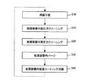
被処理基板を保持する、加熱手段を有しセラミック材料よりなる保持台と、
前記保持台を内部に備えた処理容器と、を有する成膜装置による基板処理方法であって、
前記処理容器に成膜ガスを供給して前記被処理基板に成膜を行う成膜工程と、
前記成膜工程後に、プラズマ励起されたフッ素含有クリーニングガスを前記処理容器に供給して前記処理容器内のクリーニングをするクリーニング工程と、
前記クリーニング工程後に前記処理容器内にコーティング成膜を行うコーティング工程と、を有し、
前記クリーニング工程では、プラズマ励起された前記フッ素含有クリーニングガス中のフッ素ラジカルが再結合したフッ素分子によるクリーニングが支配的となるよう前記処理容器内の圧力が20Torr以上に制御される高圧工程と、前記高圧工程よりも前記処理容器内の圧力を低くして前記処理容器内をクリーニングする低圧工程とを含み、前記低圧工程では、前記高圧工程よりも前記保持台の温度が低くされ、
前記コーティング工程では、前記成膜工程の前記被処理基板への成膜の場合より前記保持台の温度を下げて前記コーティング成膜が行われる低温成膜工程を含むことを特徴とする。
また、本発明の他の実施形態による基板処理方法は、
被処理基板を保持する、加熱手段を有しセラミック材料よりなる保持台と、
前記保持台を内部に備えた処理容器と、を有する成膜装置による基板処理方法であって、
前記処理容器に成膜ガスを供給して前記被処理基板に成膜を行う成膜工程と、
前記成膜工程後に、プラズマ励起されたフッ素含有クリーニングガスを前記処理容器に供給して前記処理容器内のクリーニングをするクリーニング工程と、
前記クリーニング工程後に前記処理容器内にコーティング成膜を行うコーティング工程と、を有し、
前記クリーニング工程では、プラズマ励起された前記フッ素含有クリーニングガス中のフッ素ラジカルが再結合したフッ素分子によるクリーニングが支配的となるよう前記処理容器内の圧力が20Torr以上に制御される高圧工程を含み、
前記コーティング工程では、前記成膜工程の前記被処理基板への成膜の場合より前記保持台の温度を下げて前記コーティング成膜が行われる低温成膜工程と、前記低温成膜工程より前記保持台の温度を高くして前記処理容器内へコーティング成膜を行う、高温成膜工程とを含むことを特徴とする。
Claims (11)
- 被処理基板を保持する、加熱手段を有しセラミック材料よりなる保持台と、
前記保持台を内部に備えた処理容器と、を有する成膜装置による基板処理方法であって、
前記処理容器に成膜ガスを供給して前記被処理基板に成膜を行う成膜工程と、
前記成膜工程後に、プラズマ励起されたフッ素含有クリーニングガスを前記処理容器に供給して前記処理容器内のクリーニングをするクリーニング工程と、
前記クリーニング工程後に前記処理容器内にコーティング成膜を行うコーティング工程と、を有し、
前記クリーニング工程では、プラズマ励起された前記フッ素含有クリーニングガス中のフッ素ラジカルが再結合したフッ素分子によるクリーニングが支配的となるよう前記処理容器内の圧力が20Torr以上に制御される高圧工程と、前記高圧工程よりも前記処理容器内の圧力を低くして前記処理容器内をクリーニングする低圧工程とを含み、前記低圧工程では、前記高圧工程よりも前記保持台の温度が低くされ、
前記コーティング工程では、前記成膜工程の前記被処理基板への成膜の場合より前記保持台の温度を下げて前記コーティング成膜が行われる低温成膜工程を含むことを特徴とする基板処理方法。 - 前記低圧工程では、前記処理容器内の圧力が10Torr以下とされることを特徴とする請求項1記載の基板処理方法。
- 前記低圧工程では、前記保持台の温度が300℃以下とされることを特徴とする請求項2記載の基板処理方法。
- 前記クリーニング工程では、前記低圧工程後に、前記高圧工程が実施されることを特徴とする請求項1乃至3のうち、いずれか1項記載の基板処理方法。
- 被処理基板を保持する、加熱手段を有しセラミック材料よりなる保持台と、
前記保持台を内部に備えた処理容器と、を有する成膜装置による基板処理方法であって、
前記処理容器に成膜ガスを供給して前記被処理基板に成膜を行う成膜工程と、
前記成膜工程後に、プラズマ励起されたフッ素含有クリーニングガスを前記処理容器に供給して前記処理容器内のクリーニングをするクリーニング工程と、
前記クリーニング工程後に前記処理容器内にコーティング成膜を行うコーティング工程と、を有し、
前記クリーニング工程では、プラズマ励起された前記フッ素含有クリーニングガス中のフッ素ラジカルが再結合したフッ素分子によるクリーニングが支配的となるよう前記処理容器内の圧力が20Torr以上に制御される高圧工程を含み、
前記コーティング工程では、前記成膜工程の前記被処理基板への成膜の場合より前記保持台の温度を下げて前記コーティング成膜が行われる低温成膜工程と、前記低温成膜工程より前記保持台の温度を高くして前記処理容器内へコーティング成膜を行う、高温成膜工程とを含むことを特徴とする基板処理方法。 - 前記コーティング工程では、前記低温成膜工程の後で、前記高温成膜工程が行われることを特徴とする請求項5記載の基板処理方法。
- 前記クリーニングガスは、NF3よりなり、前記成膜工程で成膜される膜はWを含むことを特徴とする請求項1乃至6のうち、いずれか1項記載の基板処理方法。
- 前記高圧工程では、前記保持台の温度が350℃以上とされることを特徴とする請求項7記載の基板処理方法。
- 前記低温成膜工程では、前記保持台の温度が、430℃以下とされることを特徴とする請求項1乃至8のうち、いずれか1項記載の基板処理方法。
- 前記クリーニング工程と前記コーティング工程の間に、前記処理容器内を不活性ガスでパージするパージ工程をさらに有することを特徴とする請求項1乃至9のうち、いずれか1項記載の基板処理方法。
- 請求項1乃至10のうち、いずれか1項記載の基板処理方法をコンピュータに動作させるプログラムを記憶した記録媒体。
Priority Applications (5)
| Application Number | Priority Date | Filing Date | Title |
|---|---|---|---|
| JP2005278367A JP4823628B2 (ja) | 2005-09-26 | 2005-09-26 | 基板処理方法および記録媒体 |
| CNA2006800354936A CN101273154A (zh) | 2005-09-26 | 2006-07-25 | 基板处理方法和记录介质 |
| PCT/JP2006/314612 WO2007034624A1 (ja) | 2005-09-26 | 2006-07-25 | 基板処理方法および記録媒体 |
| US12/088,153 US20090117270A1 (en) | 2005-09-26 | 2006-07-25 | Method for treating substrate and recording medium |
| KR1020087007208A KR101012959B1 (ko) | 2005-09-26 | 2006-07-25 | 기판 처리 방법 및 기록매체 |
Applications Claiming Priority (1)
| Application Number | Priority Date | Filing Date | Title |
|---|---|---|---|
| JP2005278367A JP4823628B2 (ja) | 2005-09-26 | 2005-09-26 | 基板処理方法および記録媒体 |
Publications (3)
| Publication Number | Publication Date |
|---|---|
| JP2007084908A JP2007084908A (ja) | 2007-04-05 |
| JP2007084908A5 JP2007084908A5 (ja) | 2008-07-03 |
| JP4823628B2 true JP4823628B2 (ja) | 2011-11-24 |
Family
ID=37888679
Family Applications (1)
| Application Number | Title | Priority Date | Filing Date |
|---|---|---|---|
| JP2005278367A Expired - Fee Related JP4823628B2 (ja) | 2005-09-26 | 2005-09-26 | 基板処理方法および記録媒体 |
Country Status (5)
| Country | Link |
|---|---|
| US (1) | US20090117270A1 (ja) |
| JP (1) | JP4823628B2 (ja) |
| KR (1) | KR101012959B1 (ja) |
| CN (1) | CN101273154A (ja) |
| WO (1) | WO2007034624A1 (ja) |
Families Citing this family (90)
| Publication number | Priority date | Publication date | Assignee | Title |
|---|---|---|---|---|
| JP4885025B2 (ja) * | 2007-03-26 | 2012-02-29 | 三菱重工業株式会社 | 真空処理装置および真空処理装置の運転方法 |
| WO2009034610A1 (ja) * | 2007-09-11 | 2009-03-19 | Canon Anelva Corporation | 薄膜作成装置における基板保持具上の堆積膜の剥離防止方法及び薄膜作成装置 |
| US8529704B2 (en) | 2008-06-27 | 2013-09-10 | Mitsubishi Heavy Industries, Ltd. | Vacuum processing apparatus and operating method for vacuum processing apparatus |
| US10283321B2 (en) | 2011-01-18 | 2019-05-07 | Applied Materials, Inc. | Semiconductor processing system and methods using capacitively coupled plasma |
| JP6101113B2 (ja) | 2012-03-30 | 2017-03-22 | 株式会社日立国際電気 | 半導体装置の製造方法、クリーニング方法および基板処理装置並びにプログラム |
| JP5729351B2 (ja) * | 2012-05-18 | 2015-06-03 | 信越半導体株式会社 | 半導体ウェーハの洗浄方法 |
| US9373517B2 (en) | 2012-08-02 | 2016-06-21 | Applied Materials, Inc. | Semiconductor processing with DC assisted RF power for improved control |
| US9132436B2 (en) | 2012-09-21 | 2015-09-15 | Applied Materials, Inc. | Chemical control features in wafer process equipment |
| US10256079B2 (en) | 2013-02-08 | 2019-04-09 | Applied Materials, Inc. | Semiconductor processing systems having multiple plasma configurations |
| JP6063293B2 (ja) * | 2013-02-22 | 2017-01-18 | 大陽日酸株式会社 | 気相成長方法 |
| US9362130B2 (en) | 2013-03-01 | 2016-06-07 | Applied Materials, Inc. | Enhanced etching processes using remote plasma sources |
| JP2015183260A (ja) * | 2014-03-25 | 2015-10-22 | 株式会社日立国際電気 | クリーニング方法、基板処理装置およびプログラム |
| US9309598B2 (en) | 2014-05-28 | 2016-04-12 | Applied Materials, Inc. | Oxide and metal removal |
| US9368364B2 (en) * | 2014-09-24 | 2016-06-14 | Applied Materials, Inc. | Silicon etch process with tunable selectivity to SiO2 and other materials |
| US9966240B2 (en) | 2014-10-14 | 2018-05-08 | Applied Materials, Inc. | Systems and methods for internal surface conditioning assessment in plasma processing equipment |
| US9355922B2 (en) | 2014-10-14 | 2016-05-31 | Applied Materials, Inc. | Systems and methods for internal surface conditioning in plasma processing equipment |
| US11637002B2 (en) | 2014-11-26 | 2023-04-25 | Applied Materials, Inc. | Methods and systems to enhance process uniformity |
| US10573496B2 (en) | 2014-12-09 | 2020-02-25 | Applied Materials, Inc. | Direct outlet toroidal plasma source |
| US10224210B2 (en) | 2014-12-09 | 2019-03-05 | Applied Materials, Inc. | Plasma processing system with direct outlet toroidal plasma source |
| US11257693B2 (en) | 2015-01-09 | 2022-02-22 | Applied Materials, Inc. | Methods and systems to improve pedestal temperature control |
| US20160225652A1 (en) | 2015-02-03 | 2016-08-04 | Applied Materials, Inc. | Low temperature chuck for plasma processing systems |
| US9728437B2 (en) | 2015-02-03 | 2017-08-08 | Applied Materials, Inc. | High temperature chuck for plasma processing systems |
| US9741593B2 (en) | 2015-08-06 | 2017-08-22 | Applied Materials, Inc. | Thermal management systems and methods for wafer processing systems |
| US9691645B2 (en) | 2015-08-06 | 2017-06-27 | Applied Materials, Inc. | Bolted wafer chuck thermal management systems and methods for wafer processing systems |
| US9349605B1 (en) | 2015-08-07 | 2016-05-24 | Applied Materials, Inc. | Oxide etch selectivity systems and methods |
| US10504700B2 (en) | 2015-08-27 | 2019-12-10 | Applied Materials, Inc. | Plasma etching systems and methods with secondary plasma injection |
| US10522371B2 (en) | 2016-05-19 | 2019-12-31 | Applied Materials, Inc. | Systems and methods for improved semiconductor etching and component protection |
| US10504754B2 (en) | 2016-05-19 | 2019-12-10 | Applied Materials, Inc. | Systems and methods for improved semiconductor etching and component protection |
| US10062575B2 (en) | 2016-09-09 | 2018-08-28 | Applied Materials, Inc. | Poly directional etch by oxidation |
| US10629473B2 (en) | 2016-09-09 | 2020-04-21 | Applied Materials, Inc. | Footing removal for nitride spacer |
| US10546729B2 (en) | 2016-10-04 | 2020-01-28 | Applied Materials, Inc. | Dual-channel showerhead with improved profile |
| US9934942B1 (en) | 2016-10-04 | 2018-04-03 | Applied Materials, Inc. | Chamber with flow-through source |
| US10062585B2 (en) | 2016-10-04 | 2018-08-28 | Applied Materials, Inc. | Oxygen compatible plasma source |
| US10062579B2 (en) | 2016-10-07 | 2018-08-28 | Applied Materials, Inc. | Selective SiN lateral recess |
| US9768034B1 (en) | 2016-11-11 | 2017-09-19 | Applied Materials, Inc. | Removal methods for high aspect ratio structures |
| US10163696B2 (en) | 2016-11-11 | 2018-12-25 | Applied Materials, Inc. | Selective cobalt removal for bottom up gapfill |
| US10242908B2 (en) | 2016-11-14 | 2019-03-26 | Applied Materials, Inc. | Airgap formation with damage-free copper |
| US10026621B2 (en) | 2016-11-14 | 2018-07-17 | Applied Materials, Inc. | SiN spacer profile patterning |
| US10566206B2 (en) | 2016-12-27 | 2020-02-18 | Applied Materials, Inc. | Systems and methods for anisotropic material breakthrough |
| US10403507B2 (en) | 2017-02-03 | 2019-09-03 | Applied Materials, Inc. | Shaped etch profile with oxidation |
| US10431429B2 (en) | 2017-02-03 | 2019-10-01 | Applied Materials, Inc. | Systems and methods for radial and azimuthal control of plasma uniformity |
| US10043684B1 (en) | 2017-02-06 | 2018-08-07 | Applied Materials, Inc. | Self-limiting atomic thermal etching systems and methods |
| US10319739B2 (en) | 2017-02-08 | 2019-06-11 | Applied Materials, Inc. | Accommodating imperfectly aligned memory holes |
| WO2018148062A1 (en) * | 2017-02-09 | 2018-08-16 | Applied Materials, Inc. | Plasma abatement technology utilizing water vapor and oxygen reagent |
| US10943834B2 (en) | 2017-03-13 | 2021-03-09 | Applied Materials, Inc. | Replacement contact process |
| US10319649B2 (en) | 2017-04-11 | 2019-06-11 | Applied Materials, Inc. | Optical emission spectroscopy (OES) for remote plasma monitoring |
| US11276559B2 (en) | 2017-05-17 | 2022-03-15 | Applied Materials, Inc. | Semiconductor processing chamber for multiple precursor flow |
| US11276590B2 (en) | 2017-05-17 | 2022-03-15 | Applied Materials, Inc. | Multi-zone semiconductor substrate supports |
| US10049891B1 (en) | 2017-05-31 | 2018-08-14 | Applied Materials, Inc. | Selective in situ cobalt residue removal |
| US10497579B2 (en) | 2017-05-31 | 2019-12-03 | Applied Materials, Inc. | Water-free etching methods |
| US10920320B2 (en) | 2017-06-16 | 2021-02-16 | Applied Materials, Inc. | Plasma health determination in semiconductor substrate processing reactors |
| US10541246B2 (en) | 2017-06-26 | 2020-01-21 | Applied Materials, Inc. | 3D flash memory cells which discourage cross-cell electrical tunneling |
| US10727080B2 (en) | 2017-07-07 | 2020-07-28 | Applied Materials, Inc. | Tantalum-containing material removal |
| US10541184B2 (en) | 2017-07-11 | 2020-01-21 | Applied Materials, Inc. | Optical emission spectroscopic techniques for monitoring etching |
| US10354889B2 (en) | 2017-07-17 | 2019-07-16 | Applied Materials, Inc. | Non-halogen etching of silicon-containing materials |
| US10170336B1 (en) | 2017-08-04 | 2019-01-01 | Applied Materials, Inc. | Methods for anisotropic control of selective silicon removal |
| US10043674B1 (en) | 2017-08-04 | 2018-08-07 | Applied Materials, Inc. | Germanium etching systems and methods |
| US10297458B2 (en) | 2017-08-07 | 2019-05-21 | Applied Materials, Inc. | Process window widening using coated parts in plasma etch processes |
| US10283324B1 (en) | 2017-10-24 | 2019-05-07 | Applied Materials, Inc. | Oxygen treatment for nitride etching |
| US10128086B1 (en) | 2017-10-24 | 2018-11-13 | Applied Materials, Inc. | Silicon pretreatment for nitride removal |
| US10424487B2 (en) | 2017-10-24 | 2019-09-24 | Applied Materials, Inc. | Atomic layer etching processes |
| US10256112B1 (en) | 2017-12-08 | 2019-04-09 | Applied Materials, Inc. | Selective tungsten removal |
| US10903054B2 (en) | 2017-12-19 | 2021-01-26 | Applied Materials, Inc. | Multi-zone gas distribution systems and methods |
| US11328909B2 (en) | 2017-12-22 | 2022-05-10 | Applied Materials, Inc. | Chamber conditioning and removal processes |
| US10854426B2 (en) | 2018-01-08 | 2020-12-01 | Applied Materials, Inc. | Metal recess for semiconductor structures |
| US10964512B2 (en) | 2018-02-15 | 2021-03-30 | Applied Materials, Inc. | Semiconductor processing chamber multistage mixing apparatus and methods |
| US10679870B2 (en) | 2018-02-15 | 2020-06-09 | Applied Materials, Inc. | Semiconductor processing chamber multistage mixing apparatus |
| TWI716818B (zh) | 2018-02-28 | 2021-01-21 | 美商應用材料股份有限公司 | 形成氣隙的系統及方法 |
| US10593560B2 (en) | 2018-03-01 | 2020-03-17 | Applied Materials, Inc. | Magnetic induction plasma source for semiconductor processes and equipment |
| US10319600B1 (en) | 2018-03-12 | 2019-06-11 | Applied Materials, Inc. | Thermal silicon etch |
| US10497573B2 (en) | 2018-03-13 | 2019-12-03 | Applied Materials, Inc. | Selective atomic layer etching of semiconductor materials |
| US10573527B2 (en) | 2018-04-06 | 2020-02-25 | Applied Materials, Inc. | Gas-phase selective etching systems and methods |
| US10490406B2 (en) | 2018-04-10 | 2019-11-26 | Appled Materials, Inc. | Systems and methods for material breakthrough |
| US10699879B2 (en) | 2018-04-17 | 2020-06-30 | Applied Materials, Inc. | Two piece electrode assembly with gap for plasma control |
| US10886137B2 (en) | 2018-04-30 | 2021-01-05 | Applied Materials, Inc. | Selective nitride removal |
| US10755941B2 (en) | 2018-07-06 | 2020-08-25 | Applied Materials, Inc. | Self-limiting selective etching systems and methods |
| US10872778B2 (en) | 2018-07-06 | 2020-12-22 | Applied Materials, Inc. | Systems and methods utilizing solid-phase etchants |
| US10672642B2 (en) | 2018-07-24 | 2020-06-02 | Applied Materials, Inc. | Systems and methods for pedestal configuration |
| US10892198B2 (en) | 2018-09-14 | 2021-01-12 | Applied Materials, Inc. | Systems and methods for improved performance in semiconductor processing |
| US11049755B2 (en) | 2018-09-14 | 2021-06-29 | Applied Materials, Inc. | Semiconductor substrate supports with embedded RF shield |
| US11062887B2 (en) | 2018-09-17 | 2021-07-13 | Applied Materials, Inc. | High temperature RF heater pedestals |
| US11417534B2 (en) | 2018-09-21 | 2022-08-16 | Applied Materials, Inc. | Selective material removal |
| US11682560B2 (en) | 2018-10-11 | 2023-06-20 | Applied Materials, Inc. | Systems and methods for hafnium-containing film removal |
| US11121002B2 (en) | 2018-10-24 | 2021-09-14 | Applied Materials, Inc. | Systems and methods for etching metals and metal derivatives |
| KR20200048162A (ko) * | 2018-10-29 | 2020-05-08 | 삼성전자주식회사 | 박막 증착 챔버의 세정 방법 |
| US11437242B2 (en) | 2018-11-27 | 2022-09-06 | Applied Materials, Inc. | Selective removal of silicon-containing materials |
| US11721527B2 (en) | 2019-01-07 | 2023-08-08 | Applied Materials, Inc. | Processing chamber mixing systems |
| US10920319B2 (en) | 2019-01-11 | 2021-02-16 | Applied Materials, Inc. | Ceramic showerheads with conductive electrodes |
| JP7333758B2 (ja) * | 2020-01-23 | 2023-08-25 | 東京エレクトロン株式会社 | 成膜方法及び成膜装置 |
| JP2022151131A (ja) * | 2021-03-26 | 2022-10-07 | 東京エレクトロン株式会社 | クリーニング方法及びプラズマ処理装置 |
Family Cites Families (11)
| Publication number | Priority date | Publication date | Assignee | Title |
|---|---|---|---|---|
| US5788778A (en) * | 1996-09-16 | 1998-08-04 | Applied Komatsu Technology, Inc. | Deposition chamber cleaning technique using a high power remote excitation source |
| US5824375A (en) * | 1996-10-24 | 1998-10-20 | Applied Materials, Inc. | Decontamination of a plasma reactor using a plasma after a chamber clean |
| JP3476638B2 (ja) * | 1996-12-20 | 2003-12-10 | 東京エレクトロン株式会社 | Cvd成膜方法 |
| JP3624628B2 (ja) * | 1997-05-20 | 2005-03-02 | 東京エレクトロン株式会社 | 成膜方法及び成膜装置 |
| JP2000003907A (ja) * | 1998-06-13 | 2000-01-07 | Tokyo Electron Ltd | クリーニング方法及びクリーニングガス生成装置 |
| JP4547744B2 (ja) * | 1999-11-17 | 2010-09-22 | 東京エレクトロン株式会社 | プリコート膜の形成方法、成膜装置のアイドリング方法、載置台構造及び成膜装置 |
| JP4713759B2 (ja) * | 2001-05-01 | 2011-06-29 | 東芝モバイルディスプレイ株式会社 | 半導体装置の製造方法 |
| JP3854157B2 (ja) * | 2002-01-15 | 2006-12-06 | 株式会社日立国際電気 | 半導体製造装置及びそのクリーニング方法 |
| JP2004179426A (ja) * | 2002-11-27 | 2004-06-24 | Tokyo Electron Ltd | 基板処理装置のクリーニング方法 |
| JP4043488B2 (ja) * | 2003-02-04 | 2008-02-06 | 東京エレクトロン株式会社 | 処理システム及び処理システムの稼動方法 |
| JP4131677B2 (ja) * | 2003-03-24 | 2008-08-13 | 株式会社日立国際電気 | 半導体デバイスの製造方法及び基板処理装置 |
-
2005
- 2005-09-26 JP JP2005278367A patent/JP4823628B2/ja not_active Expired - Fee Related
-
2006
- 2006-07-25 CN CNA2006800354936A patent/CN101273154A/zh active Pending
- 2006-07-25 WO PCT/JP2006/314612 patent/WO2007034624A1/ja active Application Filing
- 2006-07-25 US US12/088,153 patent/US20090117270A1/en not_active Abandoned
- 2006-07-25 KR KR1020087007208A patent/KR101012959B1/ko active IP Right Grant
Also Published As
| Publication number | Publication date |
|---|---|
| US20090117270A1 (en) | 2009-05-07 |
| JP2007084908A (ja) | 2007-04-05 |
| WO2007034624A1 (ja) | 2007-03-29 |
| CN101273154A (zh) | 2008-09-24 |
| KR20080039514A (ko) | 2008-05-07 |
| KR101012959B1 (ko) | 2011-02-08 |
Similar Documents
| Publication | Publication Date | Title |
|---|---|---|
| JP4823628B2 (ja) | 基板処理方法および記録媒体 | |
| US8021717B2 (en) | Film formation method, cleaning method and film formation apparatus | |
| TWI821285B (zh) | 處理基板的方法及保護處理腔室的方法 | |
| US7713354B2 (en) | Film forming method, film forming system and recording medium | |
| US20080044593A1 (en) | Method of forming a material layer | |
| US9502233B2 (en) | Method for manufacturing semiconductor device, method for processing substrate, substrate processing device and recording medium | |
| TWI403607B (zh) | The Ti-based film deposition method and storage medium | |
| JP6647260B2 (ja) | 半導体装置の製造方法、基板処理装置及びプログラム | |
| JP5208756B2 (ja) | Ti系膜の成膜方法および記憶媒体 | |
| JP7064577B2 (ja) | 基板処理装置、半導体装置の製造方法およびプログラム | |
| US7906442B2 (en) | Gas treatment method and computer readable storage medium | |
| JP7065178B2 (ja) | 半導体装置の製造方法、基板処理装置およびプログラム | |
| KR20230104735A (ko) | 기판 처리 방법, 프로그램, 기판 처리 장치 및 반도체 장치의 제조 방법 | |
| US7972961B2 (en) | Purge step-controlled sequence of processing semiconductor wafers | |
| EP4156236A1 (en) | Substrate processing apparatus, cleaning method, and method of manufacturing semiconductor device | |
| WO2024069763A1 (ja) | 基板処理方法、半導体装置の製造方法、基板処理装置、及びプログラム | |
| JP7110468B2 (ja) | 半導体装置の製造方法、基板処理装置、プログラム及び基板処理方法。 | |
| WO2022059325A1 (ja) | 半導体装置の製造方法、プログラム、基板処理装置及び基板処理方法 | |
| US20220216061A1 (en) | Substrate processing method, method of manufacturing semiconductor device, non-transitory computer-readable recording medium and substrate processing apparatus | |
| US20230037898A1 (en) | Method of manufacturing semiconductor device, substrate processing apparatus, recording medium, and method of processing substrate | |
| KR20240034774A (ko) | 코팅 방법, 처리 장치, 프로그램, 기판 처리 방법 및 반도체 장치의 제조 방법 | |
| WO2021207540A1 (en) | Apparatuses and methods of protecting nickel and nickel containing components with thin films |
Legal Events
| Date | Code | Title | Description |
|---|---|---|---|
| A521 | Request for written amendment filed |
Free format text: JAPANESE INTERMEDIATE CODE: A523 Effective date: 20080519 |
|
| A621 | Written request for application examination |
Free format text: JAPANESE INTERMEDIATE CODE: A621 Effective date: 20080519 |
|
| A131 | Notification of reasons for refusal |
Free format text: JAPANESE INTERMEDIATE CODE: A131 Effective date: 20110531 |
|
| A521 | Request for written amendment filed |
Free format text: JAPANESE INTERMEDIATE CODE: A523 Effective date: 20110727 |
|
| TRDD | Decision of grant or rejection written | ||
| A01 | Written decision to grant a patent or to grant a registration (utility model) |
Free format text: JAPANESE INTERMEDIATE CODE: A01 Effective date: 20110906 |
|
| A01 | Written decision to grant a patent or to grant a registration (utility model) |
Free format text: JAPANESE INTERMEDIATE CODE: A01 |
|
| A61 | First payment of annual fees (during grant procedure) |
Free format text: JAPANESE INTERMEDIATE CODE: A61 Effective date: 20110907 |
|
| R150 | Certificate of patent or registration of utility model |
Free format text: JAPANESE INTERMEDIATE CODE: R150 |
|
| FPAY | Renewal fee payment (event date is renewal date of database) |
Free format text: PAYMENT UNTIL: 20140916 Year of fee payment: 3 |
|
| LAPS | Cancellation because of no payment of annual fees |