KR20200048162A - 박막 증착 챔버의 세정 방법 - Google Patents
박막 증착 챔버의 세정 방법 Download PDFInfo
- Publication number
- KR20200048162A KR20200048162A KR1020180129915A KR20180129915A KR20200048162A KR 20200048162 A KR20200048162 A KR 20200048162A KR 1020180129915 A KR1020180129915 A KR 1020180129915A KR 20180129915 A KR20180129915 A KR 20180129915A KR 20200048162 A KR20200048162 A KR 20200048162A
- Authority
- KR
- South Korea
- Prior art keywords
- thin film
- film deposition
- deposition chamber
- residue
- plasma
- Prior art date
- Legal status (The legal status is an assumption and is not a legal conclusion. Google has not performed a legal analysis and makes no representation as to the accuracy of the status listed.)
- Ceased
Links
Images

Classifications
-
- H—ELECTRICITY
- H01—ELECTRIC ELEMENTS
- H01L—SEMICONDUCTOR DEVICES NOT COVERED BY CLASS H10
- H01L21/00—Processes or apparatus adapted for the manufacture or treatment of semiconductor or solid state devices or of parts thereof
- H01L21/67—Apparatus specially adapted for handling semiconductor or electric solid state devices during manufacture or treatment thereof; Apparatus specially adapted for handling wafers during manufacture or treatment of semiconductor or electric solid state devices or components ; Apparatus not specifically provided for elsewhere
- H01L21/67005—Apparatus not specifically provided for elsewhere
- H01L21/67011—Apparatus for manufacture or treatment
- H01L21/67017—Apparatus for fluid treatment
- H01L21/67028—Apparatus for fluid treatment for cleaning followed by drying, rinsing, stripping, blasting or the like
- H01L21/67034—Apparatus for fluid treatment for cleaning followed by drying, rinsing, stripping, blasting or the like for drying
-
- C—CHEMISTRY; METALLURGY
- C23—COATING METALLIC MATERIAL; COATING MATERIAL WITH METALLIC MATERIAL; CHEMICAL SURFACE TREATMENT; DIFFUSION TREATMENT OF METALLIC MATERIAL; COATING BY VACUUM EVAPORATION, BY SPUTTERING, BY ION IMPLANTATION OR BY CHEMICAL VAPOUR DEPOSITION, IN GENERAL; INHIBITING CORROSION OF METALLIC MATERIAL OR INCRUSTATION IN GENERAL
- C23C—COATING METALLIC MATERIAL; COATING MATERIAL WITH METALLIC MATERIAL; SURFACE TREATMENT OF METALLIC MATERIAL BY DIFFUSION INTO THE SURFACE, BY CHEMICAL CONVERSION OR SUBSTITUTION; COATING BY VACUUM EVAPORATION, BY SPUTTERING, BY ION IMPLANTATION OR BY CHEMICAL VAPOUR DEPOSITION, IN GENERAL
- C23C16/00—Chemical coating by decomposition of gaseous compounds, without leaving reaction products of surface material in the coating, i.e. chemical vapour deposition [CVD] processes
- C23C16/44—Chemical coating by decomposition of gaseous compounds, without leaving reaction products of surface material in the coating, i.e. chemical vapour deposition [CVD] processes characterised by the method of coating
- C23C16/4401—Means for minimising impurities, e.g. dust, moisture or residual gas, in the reaction chamber
- C23C16/4405—Cleaning of reactor or parts inside the reactor by using reactive gases
-
- B—PERFORMING OPERATIONS; TRANSPORTING
- B08—CLEANING
- B08B—CLEANING IN GENERAL; PREVENTION OF FOULING IN GENERAL
- B08B7/00—Cleaning by methods not provided for in a single other subclass or a single group in this subclass
-
- B—PERFORMING OPERATIONS; TRANSPORTING
- B08—CLEANING
- B08B—CLEANING IN GENERAL; PREVENTION OF FOULING IN GENERAL
- B08B7/00—Cleaning by methods not provided for in a single other subclass or a single group in this subclass
- B08B7/0035—Cleaning by methods not provided for in a single other subclass or a single group in this subclass by radiant energy, e.g. UV, laser, light beam or the like
-
- H—ELECTRICITY
- H01—ELECTRIC ELEMENTS
- H01J—ELECTRIC DISCHARGE TUBES OR DISCHARGE LAMPS
- H01J37/00—Discharge tubes with provision for introducing objects or material to be exposed to the discharge, e.g. for the purpose of examination or processing thereof
- H01J37/32—Gas-filled discharge tubes
- H01J37/32431—Constructional details of the reactor
- H01J37/3244—Gas supply means
- H01J37/32449—Gas control, e.g. control of the gas flow
-
- H—ELECTRICITY
- H01—ELECTRIC ELEMENTS
- H01J—ELECTRIC DISCHARGE TUBES OR DISCHARGE LAMPS
- H01J37/00—Discharge tubes with provision for introducing objects or material to be exposed to the discharge, e.g. for the purpose of examination or processing thereof
- H01J37/32—Gas-filled discharge tubes
- H01J37/32431—Constructional details of the reactor
- H01J37/32798—Further details of plasma apparatus not provided for in groups H01J37/3244 - H01J37/32788; special provisions for cleaning or maintenance of the apparatus
- H01J37/32853—Hygiene
- H01J37/32862—In situ cleaning of vessels and/or internal parts
-
- H—ELECTRICITY
- H01—ELECTRIC ELEMENTS
- H01L—SEMICONDUCTOR DEVICES NOT COVERED BY CLASS H10
- H01L21/00—Processes or apparatus adapted for the manufacture or treatment of semiconductor or solid state devices or of parts thereof
- H01L21/02—Manufacture or treatment of semiconductor devices or of parts thereof
-
- H—ELECTRICITY
- H05—ELECTRIC TECHNIQUES NOT OTHERWISE PROVIDED FOR
- H05H—PLASMA TECHNIQUE; PRODUCTION OF ACCELERATED ELECTRICALLY-CHARGED PARTICLES OR OF NEUTRONS; PRODUCTION OR ACCELERATION OF NEUTRAL MOLECULAR OR ATOMIC BEAMS
- H05H1/00—Generating plasma; Handling plasma
- H05H1/24—Generating plasma
- H05H1/46—Generating plasma using applied electromagnetic fields, e.g. high frequency or microwave energy
Landscapes
- Chemical & Material Sciences (AREA)
- Engineering & Computer Science (AREA)
- Physics & Mathematics (AREA)
- Plasma & Fusion (AREA)
- Analytical Chemistry (AREA)
- General Chemical & Material Sciences (AREA)
- Chemical Kinetics & Catalysis (AREA)
- Materials Engineering (AREA)
- Mechanical Engineering (AREA)
- Metallurgy (AREA)
- Organic Chemistry (AREA)
- Computer Hardware Design (AREA)
- Power Engineering (AREA)
- Condensed Matter Physics & Semiconductors (AREA)
- General Physics & Mathematics (AREA)
- Manufacturing & Machinery (AREA)
- Microelectronics & Electronic Packaging (AREA)
- Epidemiology (AREA)
- Public Health (AREA)
- Health & Medical Sciences (AREA)
- Optics & Photonics (AREA)
- Electromagnetism (AREA)
- Spectroscopy & Molecular Physics (AREA)
- Chemical Vapour Deposition (AREA)
- Drying Of Semiconductors (AREA)
Abstract
Description
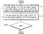
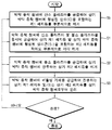
도 2 내지 도 4는 예시적인 실시예들에 따른 박막 증착 챔버의 세정 방법을 설명하기 위한 순서도들이다.
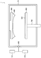
100: 가스 공급부 200: 플라즈마 발생부
300: 샤워 헤드 400: 레지듀
500: 기판 600: 지지부
700: 구동부 800: 관통부
Claims (20)
- i) 박막 증착 챔버에 산소 플라즈마 및 불소 플라즈마를 동시에 공급하여 상기 박막 증착 챔버에 형성된 탄소(C)를 포함하는 제1 레지듀 및 실리콘(Si)을 포함하는 제2 레지듀를 적어도 부분적으로 각각 제거하고; 그리고
ii) 상기 박막 증착 챔버에 불소 플라즈마를 공급하여 상기 박막 증착 챔버에 잔류하는 상기 제2 레지듀를 제거하는 것을 포함하는 박막 증착 챔버의 세정 방법. - 제1항에 있어서, i) 및 ii) 단계를 순차적으로 반복하여 수행하는 박막 증착 챔버의 세정 방법.
- 제1항에 있어서, i) 및 ii) 단계를 수행한 이후, ii) 단계를 반복적으로 수행하는 박막 증착 챔버의 세정 방법.
- 제1항에 있어서, 상기 산소 플라즈마 및 상기 불소 플라즈마는 플라즈마 발생부에 산소 소스 가스 및 불소 소스 가스를 함께 공급하여 생성되는 박막 증착 챔버의 세정 방법.
- 제4항에 있어서, 상기 플라즈마 발생부 내에서 상기 산소 소스 가스 및 상기 불소 소스 가스는 서로 반응하지 않는 박막 증착 챔버의 세정 방법.
- 제4항에 있어서, 상기 산소 소스 가스는 산소(O2)를 포함하고, 상기 불소 소스 가스는 NF3, CF4 및 C2F6로 이루어진 군에서 선택된 적어도 하나를 포함하는 박막 증착 챔버의 세정 방법.
- 제1항에 있어서, i) 단계를 수행하기 이전에, 상기 박막 증착 챔버에 형성된 상기 제1 레지듀를 부분적으로 제거하기 위하여 산소(O2) 가스 처리를 수행하는 것을 더 포함하는 박막 증착 챔버의 세정 방법.
- 제1항에 있어서, 상기 박막 증착 챔버에 비활성 기체를 공급하여 잔류하는 상기 제1 레지듀 및/또는 상기 제2 레지듀를 상기 박막 증착 챔버로부터 분리시키는 것을 더 포함하는 박막 증착 챔버의 세정 방법.
- 제8항에 있어서, 상기 비활성 기체는 헬륨(He), 아르곤(Ar) 및 네온(N2)으로 이루어진 군에서 선택된 적어도 하나 포함하는 박막 증착 챔버의 세정 방법.
- 제8항에 있어서, 상기 박막 증착 챔버에 상기 비활성 기체를 공급하는 것은 ii) 단계를 수행한 이후 수행되는 박막 증착 챔버의 세정 방법.
- 제8항에 있어서, 상기 박막 증착 챔버에 상기 비활성 기체를 공급하는 것은 i) 단계를 수행한 이후 수행되는 박막 증착 챔버의 세정 방법.
- i) 박막 증착 챔버에 산소(O2) 가스를 공급하여 상기 박막 증착 챔버에 형성된 탄소(C)를 포함하는 제1 레지듀를 부분적으로 제거하고;
ii) 상기 박막 증착 챔버에 산소 플라즈마 및 불소 플라즈마를 동시에 공급하여 상기 제1 레지듀 및 상기 박막 증착 챔버에 형성된 실리콘(Si)을 포함하는 제2 레지듀를 적어도 부분적으로 각각 제거하고; 그리고
iii) 상기 박막 증착 챔버에 불소 플라즈마를 공급하여 상기 박막 증착 챔버에 잔류하는 상기 제2 레지듀를 제거하는 것을 포함하는 박막 증착 챔버의 세정 방법. - 제12항에 있어서, i) 내지 iii) 단계를 순차적으로 반복하여 수행하는 박막 증착 챔버의 세정 방법.
- 제12항에 있어서, i) 내지 iii) 단계를 수행한 이후, ii) 및 iii) 단계를 순차적으로 반복적으로 수행하는 박막 증착 챔버의 세정 방법.
- 제12항에 있어서, 상기 박막 증착 챔버에 비활성 기체를 공급하여 잔류하는 상기 제1 레지듀 및/또는 상기 제2 레지듀를 상기 박막 증착 챔버로부터 분리시키는 것을 더 포함하는 박막 증착 챔버의 세정 방법.
- 제15항에 있어서, 상기 박막 증착 챔버에 상기 비활성 기체를 공급하는 것은 iii) 단계를 수행한 이후 수행되는 박막 증착 챔버의 세정 방법.
- i) 박막 증착 챔버에 산소 플라즈마를 공급하여 상기 박막 증착 챔버에 형성된 탄소(C)를 포함하는 제1 레지듀를 부분적으로 제거하고;
ii) 상기 박막 증착 챔버에 산소 플라즈마 및 불소 플라즈마를 동시에 공급하여 상기 제1 레지듀 및 상기 박막 증착 챔버에 형성된 실리콘(Si)을 포함하는 제2 레지듀를 적어도 부분적으로 각각 제거하고 ;
iii) 상기 박막 증착 챔버에 불소 플라즈마를 공급하여 상기 박막 증착 챔버에 잔류하는 상기 제2 레지듀를 제거하고; 그리고
iv) 상기 박막 증착 챔버에 비활성 기체를 공급하여 잔류하는 상기 제1 레지듀 및/또는 상기 제2 레지듀를 상기 박막 증착 챔버로부터 분리시키는 것을 포함하는 박막 증착 챔버의 세정 방법. - 제17항에 있어서, i) 내지 iv) 단계를 순차적으로 반복하여 수행하는 박막 증착 챔버의 세정 방법.
- 제17항에 있어서, i) 내지 iv) 단계를 수행한 이후, ii) 내지 iv) 단계를 순차적으로 반복적으로 수행하는 박막 증착 챔버의 세정 방법.
- 제17항에 있어서, i) 내지 iv) 단계를 수행한 이후, iii) 및 iv) 단계를 순차적으로 반복적으로 수행하는 박막 증착 챔버의 세정 방법.
Priority Applications (3)
| Application Number | Priority Date | Filing Date | Title |
|---|---|---|---|
| KR1020180129915A KR20200048162A (ko) | 2018-10-29 | 2018-10-29 | 박막 증착 챔버의 세정 방법 |
| US16/448,471 US20200131629A1 (en) | 2018-10-29 | 2019-06-21 | Cleaning method of a thin film deposition chamber and method of manufacturing semiconductor device using the cleaning method |
| CN201910811467.7A CN111101114A (zh) | 2018-10-29 | 2019-08-29 | 薄膜沉积腔室的清洁方法 |
Applications Claiming Priority (1)
| Application Number | Priority Date | Filing Date | Title |
|---|---|---|---|
| KR1020180129915A KR20200048162A (ko) | 2018-10-29 | 2018-10-29 | 박막 증착 챔버의 세정 방법 |
Publications (1)
| Publication Number | Publication Date |
|---|---|
| KR20200048162A true KR20200048162A (ko) | 2020-05-08 |
Family
ID=70327947
Family Applications (1)
| Application Number | Title | Priority Date | Filing Date |
|---|---|---|---|
| KR1020180129915A Ceased KR20200048162A (ko) | 2018-10-29 | 2018-10-29 | 박막 증착 챔버의 세정 방법 |
Country Status (3)
| Country | Link |
|---|---|
| US (1) | US20200131629A1 (ko) |
| KR (1) | KR20200048162A (ko) |
| CN (1) | CN111101114A (ko) |
Cited By (1)
| Publication number | Priority date | Publication date | Assignee | Title |
|---|---|---|---|---|
| WO2022145701A1 (ko) * | 2020-12-28 | 2022-07-07 | 에스케이머티리얼즈 주식회사 | F3no 가스를 이용한 반도체 및 디스플레이 화학기상 증착 챔버의 건식 세정 방법 |
Families Citing this family (1)
| Publication number | Priority date | Publication date | Assignee | Title |
|---|---|---|---|---|
| CN113053718B (zh) * | 2021-03-16 | 2022-10-28 | 江苏杰太光电技术有限公司 | 一种沉积掺杂晶硅薄膜后真空腔体的清洁方法 |
Family Cites Families (6)
| Publication number | Priority date | Publication date | Assignee | Title |
|---|---|---|---|---|
| US6841008B1 (en) * | 2000-07-17 | 2005-01-11 | Cypress Semiconductor Corporation | Method for cleaning plasma etch chamber structures |
| US7028696B2 (en) * | 2001-05-04 | 2006-04-18 | Lam Research Corporation | Plasma cleaning of deposition chamber residues using duo-step wafer-less auto clean method |
| JP4823628B2 (ja) * | 2005-09-26 | 2011-11-24 | 東京エレクトロン株式会社 | 基板処理方法および記録媒体 |
| US20070207275A1 (en) * | 2006-02-21 | 2007-09-06 | Applied Materials, Inc. | Enhancement of remote plasma source clean for dielectric films |
| US20080214007A1 (en) * | 2007-03-02 | 2008-09-04 | Texas Instruments Incorporated | Method for removing diamond like carbon residue from a deposition/etch chamber using a plasma clean |
| CN106920730A (zh) * | 2015-12-28 | 2017-07-04 | 中微半导体设备(上海)有限公司 | 一种清洁刻蚀硅基片等离子体处理装置的方法 |
-
2018
- 2018-10-29 KR KR1020180129915A patent/KR20200048162A/ko not_active Ceased
-
2019
- 2019-06-21 US US16/448,471 patent/US20200131629A1/en not_active Abandoned
- 2019-08-29 CN CN201910811467.7A patent/CN111101114A/zh active Pending
Cited By (1)
| Publication number | Priority date | Publication date | Assignee | Title |
|---|---|---|---|---|
| WO2022145701A1 (ko) * | 2020-12-28 | 2022-07-07 | 에스케이머티리얼즈 주식회사 | F3no 가스를 이용한 반도체 및 디스플레이 화학기상 증착 챔버의 건식 세정 방법 |
Also Published As
| Publication number | Publication date |
|---|---|
| US20200131629A1 (en) | 2020-04-30 |
| CN111101114A (zh) | 2020-05-05 |
Similar Documents
| Publication | Publication Date | Title |
|---|---|---|
| US9984892B2 (en) | Oxide film removing method, oxide film removing apparatus, contact forming method, and contact forming system | |
| US9034773B2 (en) | Removal of native oxide with high selectivity | |
| US7232492B2 (en) | Method of forming thin film for improved productivity | |
| KR970008333A (ko) | 화학 증착(cvd) 장치로부터 잔류물을 세척하기 위한 방법 | |
| US8097527B2 (en) | Method of forming epitaxial layer | |
| JP2004134766A (ja) | 半導体基板上への成膜方法 | |
| WO2015194380A1 (ja) | 基板処理システム及び基板処理方法 | |
| JP7782942B2 (ja) | 基板処理システム及びエッチング装置 | |
| TWI823962B (zh) | 電漿處理期間減少微粒形成之卡盤的保護層 | |
| KR20200048162A (ko) | 박막 증착 챔버의 세정 방법 | |
| US10818507B2 (en) | Method of etching silicon nitride layers for the manufacture of microelectronic workpieces | |
| JPH11224858A (ja) | Cvd装置のクリーニング方法 | |
| US9373516B2 (en) | Method and apparatus for forming gate stack on Si, SiGe or Ge channels | |
| CN114334796B (zh) | 膜层的形成方法 | |
| US20110008972A1 (en) | Methods for forming an ald sio2 film | |
| KR102819744B1 (ko) | 다색 선택도를 이용한 인접 라인들의 이방성 에칭 방법 | |
| US11527407B2 (en) | Vapor deposition of carbon-based films | |
| JPH0529285A (ja) | クリーニング方法及び半導体製造装置 | |
| US12424447B2 (en) | Method to selectively etch silicon nitride to silicon oxide using water crystallization | |
| JP2008294121A (ja) | 半導体装置の製造方法および製造装置 | |
| US12057318B2 (en) | Method for forming film layer | |
| JP4933720B2 (ja) | 成膜方法 | |
| JPH10147877A (ja) | ガスクリーニング方法 | |
| JPH06291067A (ja) | タングステン膜の成膜方法及びタングステンcvd装置 | |
| KR20240160176A (ko) | 수소 함량이 감소된 규소 함유 층들 및 이들을 제조하는 프로세스들 |
Legal Events
| Date | Code | Title | Description |
|---|---|---|---|
| PA0109 | Patent application |
Patent event code: PA01091R01D Comment text: Patent Application Patent event date: 20181029 |
|
| PG1501 | Laying open of application | ||
| A201 | Request for examination | ||
| PA0201 | Request for examination |
Patent event code: PA02012R01D Patent event date: 20210831 Comment text: Request for Examination of Application Patent event code: PA02011R01I Patent event date: 20181029 Comment text: Patent Application |
|
| E902 | Notification of reason for refusal | ||
| PE0902 | Notice of grounds for rejection |
Comment text: Notification of reason for refusal Patent event date: 20230422 Patent event code: PE09021S01D |
|
| E601 | Decision to refuse application | ||
| PE0601 | Decision on rejection of patent |
Patent event date: 20230630 Comment text: Decision to Refuse Application Patent event code: PE06012S01D Patent event date: 20230422 Comment text: Notification of reason for refusal Patent event code: PE06011S01I |